EP4006618A1 - Optical path control member and display device comprising same - Google Patents
Optical path control member and display device comprising same Download PDFInfo
- Publication number
- EP4006618A1 EP4006618A1 EP20847542.6A EP20847542A EP4006618A1 EP 4006618 A1 EP4006618 A1 EP 4006618A1 EP 20847542 A EP20847542 A EP 20847542A EP 4006618 A1 EP4006618 A1 EP 4006618A1
- Authority
- EP
- European Patent Office
- Prior art keywords
- optical path
- control member
- path control
- accommodation part
- adhesive layer
- Prior art date
- Legal status (The legal status is an assumption and is not a legal conclusion. Google has not performed a legal analysis and makes no representation as to the accuracy of the status listed.)
- Pending
Links
Images


Classifications
-
- G—PHYSICS
- G02—OPTICS
- G02B—OPTICAL ELEMENTS, SYSTEMS OR APPARATUS
- G02B26/00—Optical devices or arrangements for the control of light using movable or deformable optical elements
- G02B26/08—Optical devices or arrangements for the control of light using movable or deformable optical elements for controlling the direction of light
- G02B26/0875—Optical devices or arrangements for the control of light using movable or deformable optical elements for controlling the direction of light by means of one or more refracting elements
-
- G—PHYSICS
- G02—OPTICS
- G02F—OPTICAL DEVICES OR ARRANGEMENTS FOR THE CONTROL OF LIGHT BY MODIFICATION OF THE OPTICAL PROPERTIES OF THE MEDIA OF THE ELEMENTS INVOLVED THEREIN; NON-LINEAR OPTICS; FREQUENCY-CHANGING OF LIGHT; OPTICAL LOGIC ELEMENTS; OPTICAL ANALOGUE/DIGITAL CONVERTERS
- G02F1/00—Devices or arrangements for the control of the intensity, colour, phase, polarisation or direction of light arriving from an independent light source, e.g. switching, gating or modulating; Non-linear optics
- G02F1/01—Devices or arrangements for the control of the intensity, colour, phase, polarisation or direction of light arriving from an independent light source, e.g. switching, gating or modulating; Non-linear optics for the control of the intensity, phase, polarisation or colour
- G02F1/17—Devices or arrangements for the control of the intensity, colour, phase, polarisation or direction of light arriving from an independent light source, e.g. switching, gating or modulating; Non-linear optics for the control of the intensity, phase, polarisation or colour based on variable-absorption elements not provided for in groups G02F1/015 - G02F1/169
- G02F1/172—Devices or arrangements for the control of the intensity, colour, phase, polarisation or direction of light arriving from an independent light source, e.g. switching, gating or modulating; Non-linear optics for the control of the intensity, phase, polarisation or colour based on variable-absorption elements not provided for in groups G02F1/015 - G02F1/169 based on a suspension of orientable dipolar particles, e.g. suspended particles displays
-
- H—ELECTRICITY
- H01—ELECTRIC ELEMENTS
- H01J—ELECTRIC DISCHARGE TUBES OR DISCHARGE LAMPS
- H01J11/00—Gas-filled discharge tubes with alternating current induction of the discharge, e.g. alternating current plasma display panels [AC-PDP]; Gas-filled discharge tubes without any main electrode inside the vessel; Gas-filled discharge tubes with at least one main electrode outside the vessel
- H01J11/20—Constructional details
- H01J11/34—Vessels, containers or parts thereof, e.g. substrates
- H01J11/44—Optical arrangements or shielding arrangements, e.g. filters, black matrices, light reflecting means or electromagnetic shielding means
-
- G—PHYSICS
- G02—OPTICS
- G02B—OPTICAL ELEMENTS, SYSTEMS OR APPARATUS
- G02B26/00—Optical devices or arrangements for the control of light using movable or deformable optical elements
- G02B26/08—Optical devices or arrangements for the control of light using movable or deformable optical elements for controlling the direction of light
-
- G—PHYSICS
- G02—OPTICS
- G02B—OPTICAL ELEMENTS, SYSTEMS OR APPARATUS
- G02B5/00—Optical elements other than lenses
- G02B5/003—Light absorbing elements
-
- G—PHYSICS
- G02—OPTICS
- G02B—OPTICAL ELEMENTS, SYSTEMS OR APPARATUS
- G02B5/00—Optical elements other than lenses
- G02B5/20—Filters
- G02B5/22—Absorbing filters
- G02B5/223—Absorbing filters containing organic substances, e.g. dyes, inks or pigments
-
- G—PHYSICS
- G02—OPTICS
- G02F—OPTICAL DEVICES OR ARRANGEMENTS FOR THE CONTROL OF LIGHT BY MODIFICATION OF THE OPTICAL PROPERTIES OF THE MEDIA OF THE ELEMENTS INVOLVED THEREIN; NON-LINEAR OPTICS; FREQUENCY-CHANGING OF LIGHT; OPTICAL LOGIC ELEMENTS; OPTICAL ANALOGUE/DIGITAL CONVERTERS
- G02F1/00—Devices or arrangements for the control of the intensity, colour, phase, polarisation or direction of light arriving from an independent light source, e.g. switching, gating or modulating; Non-linear optics
- G02F1/01—Devices or arrangements for the control of the intensity, colour, phase, polarisation or direction of light arriving from an independent light source, e.g. switching, gating or modulating; Non-linear optics for the control of the intensity, phase, polarisation or colour
- G02F1/13—Devices or arrangements for the control of the intensity, colour, phase, polarisation or direction of light arriving from an independent light source, e.g. switching, gating or modulating; Non-linear optics for the control of the intensity, phase, polarisation or colour based on liquid crystals, e.g. single liquid crystal display cells
- G02F1/1323—Arrangements for providing a switchable viewing angle
-
- G—PHYSICS
- G02—OPTICS
- G02F—OPTICAL DEVICES OR ARRANGEMENTS FOR THE CONTROL OF LIGHT BY MODIFICATION OF THE OPTICAL PROPERTIES OF THE MEDIA OF THE ELEMENTS INVOLVED THEREIN; NON-LINEAR OPTICS; FREQUENCY-CHANGING OF LIGHT; OPTICAL LOGIC ELEMENTS; OPTICAL ANALOGUE/DIGITAL CONVERTERS
- G02F1/00—Devices or arrangements for the control of the intensity, colour, phase, polarisation or direction of light arriving from an independent light source, e.g. switching, gating or modulating; Non-linear optics
- G02F1/01—Devices or arrangements for the control of the intensity, colour, phase, polarisation or direction of light arriving from an independent light source, e.g. switching, gating or modulating; Non-linear optics for the control of the intensity, phase, polarisation or colour
- G02F1/13—Devices or arrangements for the control of the intensity, colour, phase, polarisation or direction of light arriving from an independent light source, e.g. switching, gating or modulating; Non-linear optics for the control of the intensity, phase, polarisation or colour based on liquid crystals, e.g. single liquid crystal display cells
- G02F1/133—Constructional arrangements; Operation of liquid crystal cells; Circuit arrangements
- G02F1/1333—Constructional arrangements; Manufacturing methods
- G02F1/1335—Structural association of cells with optical devices, e.g. polarisers or reflectors
-
- G—PHYSICS
- G02—OPTICS
- G02F—OPTICAL DEVICES OR ARRANGEMENTS FOR THE CONTROL OF LIGHT BY MODIFICATION OF THE OPTICAL PROPERTIES OF THE MEDIA OF THE ELEMENTS INVOLVED THEREIN; NON-LINEAR OPTICS; FREQUENCY-CHANGING OF LIGHT; OPTICAL LOGIC ELEMENTS; OPTICAL ANALOGUE/DIGITAL CONVERTERS
- G02F1/00—Devices or arrangements for the control of the intensity, colour, phase, polarisation or direction of light arriving from an independent light source, e.g. switching, gating or modulating; Non-linear optics
- G02F1/01—Devices or arrangements for the control of the intensity, colour, phase, polarisation or direction of light arriving from an independent light source, e.g. switching, gating or modulating; Non-linear optics for the control of the intensity, phase, polarisation or colour
- G02F1/165—Devices or arrangements for the control of the intensity, colour, phase, polarisation or direction of light arriving from an independent light source, e.g. switching, gating or modulating; Non-linear optics for the control of the intensity, phase, polarisation or colour based on translational movement of particles in a fluid under the influence of an applied field
- G02F1/1675—Constructional details
- G02F1/1676—Electrodes
-
- G—PHYSICS
- G02—OPTICS
- G02F—OPTICAL DEVICES OR ARRANGEMENTS FOR THE CONTROL OF LIGHT BY MODIFICATION OF THE OPTICAL PROPERTIES OF THE MEDIA OF THE ELEMENTS INVOLVED THEREIN; NON-LINEAR OPTICS; FREQUENCY-CHANGING OF LIGHT; OPTICAL LOGIC ELEMENTS; OPTICAL ANALOGUE/DIGITAL CONVERTERS
- G02F1/00—Devices or arrangements for the control of the intensity, colour, phase, polarisation or direction of light arriving from an independent light source, e.g. switching, gating or modulating; Non-linear optics
- G02F1/01—Devices or arrangements for the control of the intensity, colour, phase, polarisation or direction of light arriving from an independent light source, e.g. switching, gating or modulating; Non-linear optics for the control of the intensity, phase, polarisation or colour
- G02F1/165—Devices or arrangements for the control of the intensity, colour, phase, polarisation or direction of light arriving from an independent light source, e.g. switching, gating or modulating; Non-linear optics for the control of the intensity, phase, polarisation or colour based on translational movement of particles in a fluid under the influence of an applied field
- G02F1/1685—Operation of cells; Circuit arrangements affecting the entire cell
-
- H—ELECTRICITY
- H01—ELECTRIC ELEMENTS
- H01J—ELECTRIC DISCHARGE TUBES OR DISCHARGE LAMPS
- H01J11/00—Gas-filled discharge tubes with alternating current induction of the discharge, e.g. alternating current plasma display panels [AC-PDP]; Gas-filled discharge tubes without any main electrode inside the vessel; Gas-filled discharge tubes with at least one main electrode outside the vessel
- H01J11/10—AC-PDPs with at least one main electrode being out of contact with the plasma
- H01J11/12—AC-PDPs with at least one main electrode being out of contact with the plasma with main electrodes provided on both sides of the discharge space
-
- H—ELECTRICITY
- H01—ELECTRIC ELEMENTS
- H01J—ELECTRIC DISCHARGE TUBES OR DISCHARGE LAMPS
- H01J11/00—Gas-filled discharge tubes with alternating current induction of the discharge, e.g. alternating current plasma display panels [AC-PDP]; Gas-filled discharge tubes without any main electrode inside the vessel; Gas-filled discharge tubes with at least one main electrode outside the vessel
- H01J11/20—Constructional details
- H01J11/34—Vessels, containers or parts thereof, e.g. substrates
- H01J11/38—Dielectric or insulating layers
-
- G—PHYSICS
- G02—OPTICS
- G02B—OPTICAL ELEMENTS, SYSTEMS OR APPARATUS
- G02B2207/00—Coding scheme for general features or characteristics of optical elements and systems of subclass G02B, but not including elements and systems which would be classified in G02B6/00 and subgroups
- G02B2207/123—Optical louvre elements, e.g. for directional light blocking
-
- G—PHYSICS
- G02—OPTICS
- G02F—OPTICAL DEVICES OR ARRANGEMENTS FOR THE CONTROL OF LIGHT BY MODIFICATION OF THE OPTICAL PROPERTIES OF THE MEDIA OF THE ELEMENTS INVOLVED THEREIN; NON-LINEAR OPTICS; FREQUENCY-CHANGING OF LIGHT; OPTICAL LOGIC ELEMENTS; OPTICAL ANALOGUE/DIGITAL CONVERTERS
- G02F1/00—Devices or arrangements for the control of the intensity, colour, phase, polarisation or direction of light arriving from an independent light source, e.g. switching, gating or modulating; Non-linear optics
- G02F1/01—Devices or arrangements for the control of the intensity, colour, phase, polarisation or direction of light arriving from an independent light source, e.g. switching, gating or modulating; Non-linear optics for the control of the intensity, phase, polarisation or colour
- G02F1/165—Devices or arrangements for the control of the intensity, colour, phase, polarisation or direction of light arriving from an independent light source, e.g. switching, gating or modulating; Non-linear optics for the control of the intensity, phase, polarisation or colour based on translational movement of particles in a fluid under the influence of an applied field
- G02F1/166—Devices or arrangements for the control of the intensity, colour, phase, polarisation or direction of light arriving from an independent light source, e.g. switching, gating or modulating; Non-linear optics for the control of the intensity, phase, polarisation or colour based on translational movement of particles in a fluid under the influence of an applied field characterised by the electro-optical or magneto-optical effect
- G02F1/167—Devices or arrangements for the control of the intensity, colour, phase, polarisation or direction of light arriving from an independent light source, e.g. switching, gating or modulating; Non-linear optics for the control of the intensity, phase, polarisation or colour based on translational movement of particles in a fluid under the influence of an applied field characterised by the electro-optical or magneto-optical effect by electrophoresis
-
- G—PHYSICS
- G02—OPTICS
- G02F—OPTICAL DEVICES OR ARRANGEMENTS FOR THE CONTROL OF LIGHT BY MODIFICATION OF THE OPTICAL PROPERTIES OF THE MEDIA OF THE ELEMENTS INVOLVED THEREIN; NON-LINEAR OPTICS; FREQUENCY-CHANGING OF LIGHT; OPTICAL LOGIC ELEMENTS; OPTICAL ANALOGUE/DIGITAL CONVERTERS
- G02F1/00—Devices or arrangements for the control of the intensity, colour, phase, polarisation or direction of light arriving from an independent light source, e.g. switching, gating or modulating; Non-linear optics
- G02F1/01—Devices or arrangements for the control of the intensity, colour, phase, polarisation or direction of light arriving from an independent light source, e.g. switching, gating or modulating; Non-linear optics for the control of the intensity, phase, polarisation or colour
- G02F1/165—Devices or arrangements for the control of the intensity, colour, phase, polarisation or direction of light arriving from an independent light source, e.g. switching, gating or modulating; Non-linear optics for the control of the intensity, phase, polarisation or colour based on translational movement of particles in a fluid under the influence of an applied field
- G02F1/1675—Constructional details
- G02F1/1679—Gaskets; Spacers; Sealing of cells; Filling or closing of cells
- G02F1/1681—Gaskets; Spacers; Sealing of cells; Filling or closing of cells having two or more microcells partitioned by walls, e.g. of microcup type
-
- G—PHYSICS
- G02—OPTICS
- G02F—OPTICAL DEVICES OR ARRANGEMENTS FOR THE CONTROL OF LIGHT BY MODIFICATION OF THE OPTICAL PROPERTIES OF THE MEDIA OF THE ELEMENTS INVOLVED THEREIN; NON-LINEAR OPTICS; FREQUENCY-CHANGING OF LIGHT; OPTICAL LOGIC ELEMENTS; OPTICAL ANALOGUE/DIGITAL CONVERTERS
- G02F2202/00—Materials and properties
- G02F2202/28—Adhesive materials or arrangements
-
- G—PHYSICS
- G02—OPTICS
- G02F—OPTICAL DEVICES OR ARRANGEMENTS FOR THE CONTROL OF LIGHT BY MODIFICATION OF THE OPTICAL PROPERTIES OF THE MEDIA OF THE ELEMENTS INVOLVED THEREIN; NON-LINEAR OPTICS; FREQUENCY-CHANGING OF LIGHT; OPTICAL LOGIC ELEMENTS; OPTICAL ANALOGUE/DIGITAL CONVERTERS
- G02F2203/00—Function characteristic
- G02F2203/01—Function characteristic transmissive
Definitions
- An embodiment provides an optical path control member having improved driving characteristics by controlling a thickness and dielectric constant of an adhesive layer between a pattern layer and an electrode layer.
- a light-shielding film shields transmitting of light from a light source, and is attached to a front surface of a display panel which is a display device used for a mobile phone, a notebook, a tablet PC, a vehicle navigation device, a vehicle touch, etc., so that the light-shielding film adjusts a viewing angle of light according to an incident angle of light to express a clear image quality at a viewing angle needed by a user when the display transmits a screen.
- the light-shielding film may be used for the window of a vehicle, building or the like to shield outside light partially to prevent glare, or to prevent the inside from being visible from the outside.
- the light-shielding film may control the movement path of light, block light in a specific direction, and transmit light in a specific direction.
- such a light-shielding film may be applied to a display device such as a navigation device or a vehicle dashboard in a movement means such as a vehicle. That is, the light-shielding film may be applied to various fields in accordance with various purposes.
- the light-shielding film may be used in various environments of the user.
- the light-shielding film may be used during the day or night, and may be applied in various environments, such as when the user requires a specific viewing angle or improved visibility.
- An embodiment provides an optical path control member that is driven in another mode according to application of voltage and has improved driving characteristics, and a display device including the same.
- An optical path control member includes: a lower substrate; a lower electrode disposed on an upper surface of the lower substrate; an upper substrate disposed on the lower substrate; an upper electrode disposed on a lower surface of the upper substrate; a light conversion unit disposed between the lower electrode and the upper electrode; and an adhesive layer between the light conversion unit and the upper electrode, wherein the light conversion unit includes a partition wall part and an accommodation part alternately disposed, the accommodation part changes light transmittance according to application of voltage, when a ratio of a thickness and a dielectric constant (thickness/dielectric constant) of the accommodation part is defined as A, and a ratio of a thickness and a dielectric constant (thickness/dielectric constant) of the adhesive layer is defined as B, the value of A is greater than the value of B.
- An optical path control member can include a light conversion unit in which light transmittance is changed according to application of voltage.
- the light conversion unit of the optical path control member according to the embodiment can be driven as a light blocking part, and when the voltage is applied, the light conversion unit can be driven as a light transmitting part.
- the optical path control member according to the embodiment can be applied in various ways according to a user's usage environment. That is, the optical path control member according to the embodiment may be driven as a switchable light blocking film.
- an accommodation part of the light conversion unit of the optical path control member extends from a light incident part toward a light emitting part and a width of the accommodation part can be widened. Further, when the voltage is applied, since light absorbing particles are moved in a direction in which the width is narrowed, the light absorbing particles can be easily moved, thereby improving efficiency of the optical path control member.
- the accommodation part of the light conversion unit can be disposed to be spaced apart from an electrode in a direction of a visual field surface or an electrode in a direction opposite to the direction of the visual field surface to reduce a decrease in light transmission by the accommodation part and improve brightness. Accordingly, visibility of the optical path control member can be improved.
- optical path control member can control characteristics of the adhesive layer between the accommodation part and an upper electrode.
- the adhesive layer has dielectric properties
- the adhesive layer has the resistor characteristic
- the voltage transfer from the upper electrode to the accommodation part is increased by controlling the volume resistance of the adhesive layer to a specific range, thereby reducing the response speed of the optical path control member. Accordingly, it is possible to improve the driving characteristics of the optical path control member by reducing the response speed of the optical path control member.
- the terms used in the embodiments of the present invention are for describing the embodiments and are not intended to limit the present invention.
- the singular forms may also include the plural forms unless specifically stated in the phrase, and may include at least one of all combinations that may be combined in A, B, and C when described in "at least one (or more) of A (and), B, and C".
- first, second, A, B, (a), and (b) may be used. These terms are only used to distinguish the elements from other elements, and the terms are not limited to the essence, order, or order of the elements.
- an element when an element is described as being “connected”, “coupled”, or “connected” to another element, it may include not only when the element is directly “connected” to, “coupled” to, or “connected” to other elements, but also when the element is “connected”, “coupled”, or “connected” by another element between the element and other elements.
- the "on (over)” or “under (below)” may include not only when two elements are directly connected to each other, but also when one or more other elements are formed or disposed between two elements.
- optical path control member relates to a switching optical path control member that drives in various modes according to application of voltage.
- the optical path control member according to the embodiment may be used as a light blocking film.
- the optical path control member according to the embodiment may be used as a privacy film.
- an optical path control member may include a lower substrate 110, an upper substrate 120, a lower electrode 210, an upper electrode 220, and a light conversion unit 300.
- the lower substrate 110 may support the lower electrode 210.
- the lower substrate 110 may be rigid or flexible.
- the lower substrate 110 may be transparent.
- the lower substrate 110 may include a transparent substrate capable of transmitting light.
- the lower substrate 110 may include glass, plastic, or a flexible polymer film.
- the flexible polymer film may be made of any one of polyethylene terephthalate (PET), polycarbonate (PC), acrylonitrile-butadiene-styrene copolymer (ABS), polymethyl methacrylate (PMMA), polyethylene naphthalate (PEN), polyether sulfone (PES), cyclic olefin copolymer (COC), triacetylcellulose (TAC) film, polyvinyl alcohol (PVA) film, polyimide (PI) film, and polystyrene (PS), which is only an example, but the embodiment is not limited thereto.
- PET polyethylene terephthalate
- PC polycarbonate
- ABS acrylonitrile-butadiene-styrene copolymer
- PMMA polymethyl methacrylate
- PEN polyethylene naphthalate
- PES polyether sulfone
- COC cyclic
- the lower substrate 110 may be a flexible substrate having flexible characteristics.
- the lower substrate 110 may be a curved or bended substrate. That is, the optical path control member including the lower substrate 110 may also be formed to have flexible, curved, or bent characteristics. Accordingly, the optical path control member according to the embodiment may be changed to various designs.
- the lower substrate 110 may have a thickness of about 1mm or less.
- the lower electrode 210 may be disposed on one surface of the lower substrate 110.
- the lower electrode 210 may be disposed on an upper surface of the lower substrate 110. That is, the lower electrode 210 may be disposed between the lower substrate 110 and the upper substrate 120.
- the lower electrode 210 may contain a transparent conductive material.
- the lower electrode 210 may contain a metal oxide such as indium tin oxide, indium zinc oxide, copper oxide, tin oxide, zinc oxide, titanium oxide, etc.
- the lower electrode 210 may be disposed on the lower substrate 110 in a film shape.
- light transmittance of the lower electrode 210 may be about 80% or more.
- the lower electrode 210 may have a thickness of about 10nm to about 50nm.
- the lower electrode 210 may contain various metals to realize low resistance.
- the lower electrode 210 may contain at least one metal of chromium (Cr), nickel (Ni), copper (Cu), aluminum (Al), silver (Ag), molybdenum (Mo). gold (Au), titanium (Ti), and alloys thereof.
- the lower electrode 210 may include a plurality of conductive patterns.
- the lower electrode 210 may include a plurality of mesh lines intersecting each other and a plurality of mesh openings formed by the mesh lines.
- the lower electrode 210 contains a metal, visibility may be improved because the lower electrode 210 is not visible from the outside.
- the light transmittance is increased by the openings, so that the brightness of the optical path control member according to the embodiment may be improved.
- the upper substrate 120 may be disposed on the lower substrate 110.
- the upper substrate 120 may be disposed on the lower electrode 210 on the lower substrate 110.
- the upper substrate 120 may contain a material capable of transmitting light.
- the upper substrate 120 may contain a transparent material.
- the upper substrate 120 may contain the same material as or similar to the lower substrate 110 described above.
- the upper substrate 120 may include glass, plastic, or a flexible polymer film.
- the flexible polymer film may be made of any one of polyethylene terephthalate (PET), polycarbonate (PC), acrylonitrile-butadiene-styrene copolymer (ABS), polymethyl methacrylate (PMMA), polyethylene naphthalate (PEN), polyether sulfone (PES), cyclic olefin copolymer (COC), triacetylcellulose (TAC) film, polyvinyl alcohol (PVA) film, polyimide (PI) film, and polystyrene (PS), which is only an example, but the embodiment is not limited thereto.
- PET polyethylene terephthalate
- PC polycarbonate
- ABS acrylonitrile-butadiene-styrene copolymer
- PMMA polymethyl methacrylate
- PEN polyethylene naphthalate
- PES polyether sulfone
- COC cyclic
- the upper substrate 120 may be a flexible substrate having flexible characteristics.
- the upper substrate 120 may be a curved or bended substrate. That is, the optical path control member including the upper substrate 120 may also be formed to have flexible, curved, or bent characteristics. Accordingly, the optical path control member according to the embodiment may be changed to various designs.
- the upper substrate 120 may have a thickness of about 1mm or less.
- the upper electrode 220 may be disposed on one surface of the upper substrate 120.
- the upper electrode 220 may be disposed on a lower surface of the upper substrate 120. That is, the upper electrode 220 may be disposed on a surface on which the upper substrate 120 faces the lower substrate 110. That is, the upper electrode 220 may be disposed facing the lower electrode 210 on the lower substrate 110. That is, the upper electrode 220 may be disposed between the lower electrode 210 and the upper substrate 120.
- the upper electrode 220 may contain a transparent conductive material.
- the upper electrode 220 may contain a metal oxide such as indium tin oxide, indium zinc oxide, copper oxide, tin oxide, zinc oxide, titanium oxide, etc.
- the upper electrode 220 may be disposed on the lower substrate 110 in a film shape.
- the light transmittance of the upper electrode 220 may be about 80% or more.
- the upper electrode 220 may have a thickness of about 10nm to about 50nm.
- the upper electrode 220 may contain various metals to realize low resistance.
- the upper electrode 120 may contain at least one metal of chromium (Cr), nickel (Ni), copper (Cu), aluminum (Al), silver (Ag), molybdenum (Mo). gold (Au), titanium (Ti), and alloys thereof.
- the upper electrode 220 may include a plurality of conductive patterns.
- the upper electrode 220 may include a plurality of mesh lines intersecting each other and a plurality of mesh openings formed by the mesh lines.
- the upper electrode 220 contains a metal
- visibility may be improved because the upper electrode 220 is not visible from the outside.
- the light transmittance is increased by the openings, so that the brightness of the optical path control member according to the embodiment may be improved.
- the light conversion unit 300 may be disposed between the lower substrate 110 and the upper substrate 120. In detail, the light conversion unit 300 may be disposed between the lower electrode 210 and the upper electrode 220.
- the light conversion unit 300 may include a partition wall part 310, and an accommodation part 320.
- the partition wall part 310 may be defined as a partition wall region for partitioning a region of the light conversion unit, and the accommodation part 320 may be defined as a variable region that is variable to a light blocking unit and a light transmitting unit according to application of voltage.
- the partition wall part 310 and the accommodation part 320 may be alternately disposed.
- the partition wall part 310 and the accommodation part 320 may be disposed in different widths.
- the width of the accommodation part 320 may be greater than the width of the accommodation part 320.
- the partition wall part 310 and the accommodation part 320 may be disposed in contact with at least one of the lower electrode 210 and the upper electrode 220.
- the partition wall part 310 and the accommodation part 320 may be disposed in direct contact with the lower electrode 210 and may be disposed in indirect contact with the upper electrode 220. That is, an adhesive layer 400 for adhering the lower substrate 110 and the upper substrate 120 may be disposed on the light conversion unit 300, and the partition wall part 310 and the accommodation part 320 may be disposed in indirect contact with the upper electrode 220.
- the adhesive layer 400 may be disposed between the light conversion unit 300 and the upper electrode 220.
- the adhesive layer 400 may have dielectric properties or resistor properties.
- the adhesive layer 400 may have the dielectric or resistor properties so that a voltage at the upper electrode 220 on the adhesive layer may be easily transferred to the accommodation part 320 of the light conversion unit 300.
- the adhesive layer 400 will be described in detail below.
- the embodiment is not limited thereto, and the partition wall part 310 and the accommodation part 320 may be disposed to be spaced apart from the lower electrode 210 and the upper electrode 220.
- a buffer layer for improving adhesion between the lower electrode 210 and the light conversion unit 300 may be disposed between the lower electrode 210 and the light conversion unit 300. Accordingly, the partition wall part 310 and the accommodation part 320 may be disposed to be spaced apart from both the lower electrode 210 and the upper electrode 220.
- the partition wall part 310 and the accommodation part 320 may be alternately disposed.
- the partition wall part 310 and the accommodation part 320 may be alternately disposed. That is, each of the partition wall parts 310 may be disposed between the accommodation parts 320 adjacent to each other, and each of the accommodation parts 320 may be disposed between the partition wall parts 310 adjacent to each other.
- the partition wall part 310 may contain a transparent material.
- the partition wall part 310 may contain a material that may transmit light.
- the partition wall part 310 may contain a resin material.
- the partition wall part 310 may contain a photo-curable resin material.
- the partition wall part 310 may contain a UV resin or a transparent photoresist resin.
- the partition wall part 310 may contain urethane resin or acrylic resin.
- the partition wall part 310 may transmit light incident on any one of the lower substrate 110 and the upper substrate 120 toward another substrate.
- light may be incident in a direction of the lower substrate 110 and the light may be emitted to the lower substrate 110.
- the partition wall part 310 may transmit the light, and the transmitted light may be moved in a direction of the upper substrate 120.
- the accommodation part 320 may include an electrolyte 320a and light absorbing particles 320b.
- the accommodation part 320 is filled with the electrolyte 320a, and a plurality of the light absorbing particles 320b may be dispersed in the electrolyte 320a. That is, a light conversion material containing the electrolyte 320a and the light absorbing particles 320b may be accommodated in the accommodation part 320.
- the electrolyte 320a may be a material for dispersing the light absorbing particles 320b.
- the electrolyte 320a may contain a transparent material.
- the electrolyte 320a may contain a paraffinic solvent.
- the electrolyte 320a may contain a material capable of transmitting light.
- the light absorbing particles 320b may be disposed to be dispersed in the electrolyte 320a.
- the plurality of light absorbing particles 320b may be disposed to be spaced apart from each other in the electrolyte 320a.
- the light absorbing particles 320b may include a color.
- the light absorbing particles 320b may include black light absorbing particles.
- the light absorbing particles 320b may include carbon black.
- the light absorbing particles 320b may be formed in a spherical shape.
- the light absorbing particles 320b may have a diameter of several nanometers.
- the accommodation part 320 may be changed in the light transmittance by the light absorbing particles 320b.
- the light transmittance of the accommodation part 320 may be changed to a light blocking part and a light transmitting part by the light absorbing particles 320b.
- the optical path control member according to the embodiment may be changed from a first mode to a second mode or from the second mode to the first mode by a voltage applied to the first electrode 210 and the second electrode 220.
- the optical path control member may be driven while changing from the initial mode to the first mode and the second mode according to application of voltage.
- the accommodation part 320 becomes the light blocking part in the first mode, and light of a specific angle may be blocked by the accommodation part 320. That is, a viewing angle of a user viewing from the outside may be narrowed.
- the light absorbing particles 320b are uniformly dispersed in the electrolyte 320a so that the accommodation part 320 may block the light by the light absorbing particles.
- the accommodation part 320 becomes the light transmitting part in the second mode, and in the optical path control member according to the embodiment, light may be transmitted through both the partition wall part 310 and the accommodation part 320. That is, the viewing angle of the user viewing from the outside may be widened.
- the light absorbing particles 320b are agglomerated into one region of the electrolyte 320a so that the accommodation part 320 may transmit light by the electrolyte.
- Switching from the first mode to the second mode that is, the conversion of the accommodation part 320 from the light blocking part to the light transmitting part may be realized by movement of the light absorbing particles 320b of the accommodation part 320.
- the accommodation part 320 may be electrically connected to the lower electrode 210 and the upper electrode 220.
- the accommodation part 320 may block light by the light absorbing particles. Accordingly, in the first mode, the accommodation part 320 may be driven as the light blocking part.
- the light absorbing particles 320b may move.
- the light absorbing particles 320b may move toward one end or the other end of the accommodation part 320 by a voltage transmitted through the lower electrode 210 and the upper electrode 220 to be agglomerated. That is, the light absorbing particles 320b may move from the accommodation part 320 toward the lower electrode or the upper electrode to be agglomerated.
- the light absorbing particles including the carbon black may be charged.
- micelles may be formed and a charging effect may be created by charging the carbon black light absorbing particles themselves with a negative charge or chemically introducing a functional group similar to a surfactant to a surface of the carbon black light absorbing particles to charge the light absorbing particles.
- the light absorbing particles 320b may be uniformly dispersed in the electrolyte 320a to drive the accommodation part 320 as the light blocking part.
- the light absorbing particles 320b may be moved toward the upper electrode 220 in the electrolyte 320a. That is, the light absorbing particles 320b are moved in one direction, and the accommodation part 320 may be driven as the light transmitting part.
- the optical path control member according to the embodiment may be driven in two modes according to a user's surrounding environment. That is, when the user requires light transmission only at a specific viewing angle, the accommodation part is driven as the light blocking part, or in an environment in which the user requires high brightness, a voltage may be applied to drive the accommodation part as the light transmitting part.
- the optical path control member according to the embodiment may be implemented in two modes according to the user's requirement, the optical path control member may be applied regardless of the user's environment.
- the accommodation part 320 may be formed in various shapes.
- a width of the accommodation part 320 may be changed while the accommodation part 320 extends from one end of the accommodation part 320 to the other end thereof.
- the accommodation part 320 may be formed in a trapezoidal shape.
- the accommodation part 320 may be formed so that the width of the accommodation part 320 is widened while extending from the lower electrode 210 toward the upper electrode 220.
- the width of the accommodation part 320 may be narrowed while extending from a visual field surface of the user toward an opposite surface thereof.
- the light absorbing particles of the accommodation part 320 may be moved in a direction in which the width of the accommodation part is narrowed.
- the width of the of the accommodation part 320 may be widened while extending from a light incident part in which light is incident toward a light emitting part in which light is emitted.
- the light absorbing particles of the accommodation part 320 may be moved toward the lower electrode 210.
- the light absorbing particles are moved toward the opposite surface of the visual field surface instead of the visual field surface, it is possible to prevent blocking of light emitted toward the visual field surface, thereby improving the brightness of the optical path control member.
- the light absorbing particles are moved from a wide region toward a narrow region, the light absorbing particles may be easily moved.
- the accommodation part 320 may be formed so that the width of the accommodation part 320 is narrowed while extending from the lower electrode 210 toward the upper electrode 220.
- the width of the accommodation part 320 may be widened while extending from the visual field surface of the user toward the opposite surface thereof.
- the light absorbing particles of the accommodation part 320 may be moved in a direction in which the width of the accommodation part is widened.
- the width of the of the accommodation part 320 may be narrowed while extending from the light incident part in which the light is incident toward the light emitting part in which the light is emitted.
- the light absorbing particles of the of the accommodation part 320 may be moved toward the lower electrode 210.
- a contact region between the lower electrode and one surface of the accommodation part through which the light absorbing particles move is increased, so that a moving speed of the light absorbing particles, that is, a driving speed may be increased.
- the accommodation part 320 may be disposed to be spaced apart from the lower electrode 210 or the upper electrode 220.
- the accommodation part 320 is formed to partially pass through the light conversion unit 300, and accordingly, a base part may be disposed between the accommodation part 320 and the first electrode 210.
- the base part may include the same material as the partition wall part 310 and may be integrally formed with the partition wall part 310.
- the accommodation part 320 may be disposed to be spaced apart from the first electrode 210.
- the brightness of the optical path control member may be improved by increasing transmittance of light emitted toward the visual field surface, thereby improving visibility thereof.
- the adhesive layer 400 may be disposed between the light conversion unit 300 and the upper electrode 220 in order to adhere the light conversion unit 300 on the lower substrate 110 and the upper electrode 220 on the upper substrate 120 to each other.
- the adhesive layer 400 may include a material capable of transmitting light so that light passing through the pattern part in the lower substrate 110 is emitted toward the upper substrate 120.
- the adhesive layer 400 may have light transmittance of about 85% or more, a haze of about 1.0 or less, and a chromaticity index (b ⁇ ) of about 0.2 or less.
- the adhesive layer 400 may be formed to have a thickness of about 5 ⁇ m to 100 ⁇ m. In detail, the adhesive layer 400 may be formed to have a thickness of about 5 ⁇ m to 30 ⁇ m.
- the thickness of the adhesive layer 400 When the thickness of the adhesive layer 400 is less than about 5 ⁇ m, an adhesive force between the light conversion unit 300 and the upper electrode 220 may be reduced, and thus the reliability of the optical path control member may be deteriorated. In addition, when the thickness of the adhesive layer 400 exceeds about 150 ⁇ m, a thickness of the optical path control member may increase, and as the number of paths in which a voltage is applied from the upper electrode 220 toward the light conversion unit 300 is increased, voltage loss may be increased.
- the voltage transmitted from the upper electrode 220 may be applied to the accommodation part 320 of the light conversion unit 300 to move the light absorbing particles 320b inside the accommodation part 320.
- the movement of the light absorbing particles in the accommodation part 320 may be smoothed, thereby improving driving characteristics of the optical path control member.
- the adhesive layer 400 may have the dielectric properties or resistor properties, whereby a voltage may be transferred from the upper electrode 220 to the accommodation part 320 via the adhesive layer 400.
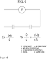
- a driving speed for the movement of the light absorbing particles in the accommodation part may be defined by the following equation.
- Electrophoretic mobility ⁇ E terminal velocity applied electric field
- E E Voltage V Electrode distance d
- a response time t related to the driving speed for the movement of the light absorbing particles in the accommodation part decreases as an electrophoretic mobility is large, a voltage is large, and a distance between electrodes is small.
- a voltage applied to the accommodation part should be increased in order to improve the driving characteristics of the optical path control member by making the response speed of the optical path control member small, that is, fast.
- the adhesive layer 400 may have the dielectric properties or resistor properties.
- the adhesive layer 400 may have the dielectric properties.
- the optical path control member becomes a capacitor in which the adhesive layer 400 and the accommodation part 320 are connected in series, and it can be seen that the voltage of the adhesive layer 400 needs to be high in order to apply more voltage to the accommodation part 320.
- the adhesive layer 400 may have the dielectric properties, and a dielectric constant and a thickness T2 of the adhesive layer 400 and a dielectric constant and a thickness T1 of the accommodation part 320 may be controlled.
- an electric capacity of the adhesive layer and the accommodation part is proportional to the dielectric constant and inversely proportional to the thickness, and the voltage of the adhesive layer and the accommodation part may be inversely proportional to the dielectric constant and may be proportional to the thickness.
- the dielectric constant of the accommodation part should be small and the thickness should be large, and in order to increase the voltage applied to the accommodation part, the electric capacity of the adhesive layer 400 should be increased. That is, in case of the adhesive layer, the electric capacity of the adhesive layer may be increased when the dielectric constant is large and the thickness is small.
- a value of A may be greater than a value of B.
- the ratio A of the thickness and the dielectric constant of the accommodation part 320 may be as large as 5 times or more with respect to the ratio B of the thickness and the dielectric constant of the adhesive layer 400.
- the ratio A of the thickness and the dielectric constant of the accommodation part 320 may be as large as 10 times or more with respect to the ratio B of the thickness and the dielectric constant of the adhesive layer 400.
- the accommodation part 320 may have a dielectric constant (F/m) of 2 to 4, may have a thickness of about 40 ⁇ m to 150 ⁇ m, and the ratio A of the thickness and the dielectric constant of the accommodation part 320 may be about 20 to 40.
- the adhesive layer 400 may have a dielectric constant (F/m) of 2 to 9, may have a thickness of about 5 ⁇ m to 100 ⁇ m, and the ratio B of the thickness and the dielectric constant of the adhesive layer 400 may be 1 to 50.
- the optical path control member may set so that the ratio A of the thickness and the dielectric constant of the accommodation part 320 becomes 5 times or more and preferably 10 times or more with respect to the ratio B of the thickness and the dielectric constant of the adhesive layer 400.
- the adhesive layer 400 has a small thickness and a large dielectric constant
- the electric capacity of the adhesive layer 400 may be increased so that a larger voltage is applied to the accommodation part 320.
- the response speed of the optical path control member may be increased by increasing the voltage applied to the accommodation part 320, thereby improving the driving characteristics of the optical path control member.
- the adhesive layer 400 may have the resistor properties.
- the optical path control member becomes an RC circuit in which the adhesive layer 400 and the accommodation part 320 are connected in series, and in the RC circuit, when a predetermined time has elapsed, all electromotive force may be applied to the capacitor.
- the adhesive layer 400 may have a volume resistance of about 10 7 Qcm or more. In detail, the adhesive layer 400 may have a volume resistance of about 10 7 Qcm to 10 12 Qcm.
- the volume resistance of the adhesive layer 400 is less than 10 7 Qcm, the conductivity of the adhesive layer 400 is too increased, so that the upper electrode 220 and the adhesive layer 400 are energized, and when the volume resistance of the adhesive layer 400 exceeds 10 12 Qcm, the conductivity of the adhesive layer 400 is too decreased, so that voltage transfer efficiency from the upper electrode 220 to the accommodation part 320 may be reduced.
- the optical path control member according to the embodiment may include the pattern part in which the light transmittance is changed according to application of voltage.
- the pattern part of the optical path control member according to the embodiment may be driven as the light blocking part, and when the voltage is applied, the pattern part may be driven as the light transmitting part.
- optical path control member according to the embodiment may be applied in various ways according to a user's usage environment.
- the width of the pattern part may be widened while the pattern part of the optical path control member according to the embodiment extends from the light incident part toward the light emitting part. Further, when the voltage is applied, since beads are moved in the direction in which the width is narrowed, the beads may be easily moved, thereby improving efficiency of the optical path control member.
- the pattern part may be disposed to be spaced apart from the electrode in the direction of the visual field surface or the electrode in the direction opposite to the direction of the visual field surface to reduce a decrease in light transmission by the pattern part and improve brightness. Accordingly, visibility of the optical path control member may be improved.
- optical path control member may control characteristics of the adhesive layer between the accommodation part and the upper electrode serving as a variable pattern part.
- the adhesive layer has the dielectric properties
- the adhesive layer has the resistor characteristic
- the voltage transfer from the upper electrode to the accommodation part is increased by controlling the volume resistance of the adhesive layer to a specific range, thereby reducing the response speed of the optical path control member. Accordingly, it is possible to improve the driving characteristics of the optical path control member by reducing the response speed of the optical path control member.
- an electrode material forming a lower substrate 110 and a lower electrode is prepared.
- the electrode material may be formed on one surface of the lower substrate 110 by a coating or deposition process.
- the electrode material may be formed on the entire surface of the lower substrate 110. Accordingly, a lower electrode 210 formed as a surface electrode may be formed on the lower substrate 110.
- a resin layer may be formed by applying a resin material on the lower electrode 210.
- the resin layer may be formed by applying a urethane resin or an acrylic resin on the lower electrode 210.
- a pattern part may be formed on the resin layer using a mold.
- holes or grooves are formed in the resin layer by imprinting the mold, and accordingly, a partition wall part may be formed by the remaining resin layer. That is, the partition wall part 310 and the accommodation part 320 described above may be formed on the resin layer.
- an electrode material forming an upper substrate 120 and an upper electrode is prepared.
- the electrode material may be formed on one surface of the upper substrate 120 by a coating or deposition process.
- the electrode material may be formed on the entire surface of the upper substrate 120.
- an upper electrode 220 formed as a surface electrode may be formed on the upper substrate 120.
- an adhesive layer 400 may be formed by applying an adhesive material on the upper electrode 220.
- the adhesive layer 400 may be formed on a partial region of the upper electrode 220.
- the lower substrate 110 and the upper substrate 120 manufactured in advance may be adhered.
- the lower substrate 110 and the upper substrate 120 may be adhered to each other through the adhesive layer 400 on the upper substrate 120.
- the lower substrate 110 and the upper substrate 120 may be adhered in different directions.
- the lower substrate 110 and the upper substrate 120 may be adhered to each other so that a long side direction of the lower substrate 110 and a short side direction of the upper substrate 120 overlap each other.
- a dam part 600 may be formed on the lower substrate 110.
- the dam part 600 may be disposed above and below the accommodation part 320 disposed on the lower substrate 110. That is, the dam part 600 may be disposed so that the accommodation part 320 is disposed between the dam parts 600.
- a light conversion material may be injected between the accommodation part 320, that is, the partition wall parts 310.
- a light conversion material in which light absorbing particles such as carbon black or the like are dispersed in an electrolyte solvent containing a paraffinic solvent may be injected between the accommodation part 320, that is, between the partition wall parts. Accordingly, the accommodation part 310 described above may be formed between the partition wall parts 310.
- the light conversion material inside the accommodation part may be sealed from the outside by forming a sealing part 500 in the lateral direction of the accommodation part 320.
- a final optical path control member may be formed by cutting the lower substrate 110.
- FIGS. 19 to 21 a display device and a display apparatus to which an optical path control member according to an embodiment is applied will be described.
- an optical path control member 1000 may be disposed on a display panel 2000.
- the display panel 2000 and the optical path control member 1000 may be disposed to be adhered to each other.
- the display panel 2000 and the optical path control member 1000 may be adhered to each other via an adhesive layer 1500.
- the adhesive layer 1500 may be transparent.
- the adhesive layer 1500 may include an adhesive or an adhesive layer containing an optical transparent adhesive material.
- the adhesive layer 1500 may include a release film.
- the optical path control member and the display panel may be adhered after the release film is removed.
- the display panel 2000 may include a first substrate 2100 and a second substrate 2200.
- the display panel 2000 may be formed in a structure in which the first substrate 2100 including a thin film transistor (TFT) and a pixel electrode and the second substrate 2200 including color filter layers are bonded with a liquid crystal layer interposed therebetween.
- TFT thin film transistor
- the display panel 2000 may be a liquid crystal display panel of a color filter on transistor (COT) structure in which a thin film transistor, a color filter, and a black matrix are formed at a first substrate 2100 and a second substrate 2200 is bonded to the first substrate 2100 with a liquid crystal layer interposed therebetween. That is, a thin film transistor may be formed on the first substrate 2100, a protective film may be formed on the thin film transistor, and a color filter layer may be formed on the protective film. In addition, a pixel electrode in contact with the thin film transistor may be formed on the first substrate 2100. At this point, in order to improve an aperture ratio and simplify a masking process, a black electrolyte 320aay be omitted, and a common electrode may be formed to function as the black matrix.
- COT color filter on transistor
- the display device may further include a backlight unit providing light from a rear surface of the display panel 2000.
- the display panel 2000 when the display panel 2000 is an organic electroluminescence display panel, the display panel 2000 may include a self-luminous element that does not require a separate light source.
- a thin film transistor may be formed on the first substrate 2100, and an organic light emitting element in contact with the thin film transistor may be formed.
- the organic light emitting element may include an anode, a cathode, and an organic light emitting layer formed between the anode and the cathode.
- a second substrate 2200 configured to function as an encapsulation substrate for encapsulation may further be included on the organic light emitting element.
- a polarizing plate may be further disposed between the optical path control member 1000 and the display panel 2000.
- the polarizing plate may be a linear polarizing plate or an external light reflection preventive polarizing plate.
- the polarizing plate may be the linear polarizing plate.
- the polarizing plate may be the external light reflection preventive polarizing plate.
- an additional functional layer 1300 such as an anti-reflection layer, an anti-glare, or the like may be further disposed on the optical path control member 1000.
- the functional layer 1300 may be adhered to one surface of the base substrate 100 of the optical path control member.
- the functional layer 1300 may be adhered to the base 100 of the optical path control member via an adhesive layer.
- a release film for protecting the functional layer may be further disposed on the functional layer 1300.
- a touch panel may be further disposed between the display panel and the optical path control member.
- the optical path control member is disposed at an upper portion of the display panel, but the embodiment is not limited thereto, and the optical path control member may be disposed at various positions such as a position in which light is adjustable, that is, a lower portion of the display panel, between an upper substrate and a lower substrate of the display panel, or the like.
- an optical path control member may be applied to a display device that displays a display.
- the accommodation part when power is not applied to the optical path control member as shown in FIG. 20 , the accommodation part functions as the light blocking part, so that the display device is driven in a light blocking mode, and when power is applied to the optical path control member as shown in FIG. 21 , the accommodation part functions as the light transmitting part, so that the display device may be driven in an open mode.
- a user may easily drive the display device in a privacy mode or a normal mode according to application of power.
- the display device to which the optical path control member according to the embodiment is applied may also be applied inside a vehicle.
- the display device including the optical path control member according to the embodiment may display a video confirming information of the vehicle and a movement route of the vehicle.
- the display device may be disposed between a driver seat and a passenger seat of the vehicle.
- optical path control member according to the embodiment may be applied to a dashboard that displays a speed, an engine, an alarm signal, and the like of the vehicle.
- optical path control member according to the embodiment may be applied to a windshield of the vehicle or right and left window glasses.
Landscapes
- Physics & Mathematics (AREA)
- Nonlinear Science (AREA)
- Optics & Photonics (AREA)
- General Physics & Mathematics (AREA)
- Chemical & Material Sciences (AREA)
- Plasma & Fusion (AREA)
- Engineering & Computer Science (AREA)
- Crystallography & Structural Chemistry (AREA)
- Health & Medical Sciences (AREA)
- Life Sciences & Earth Sciences (AREA)
- Chemical Kinetics & Catalysis (AREA)
- Electrochemistry (AREA)
- Molecular Biology (AREA)
- Mathematical Physics (AREA)
- Electromagnetism (AREA)
- Electrochromic Elements, Electrophoresis, Or Variable Reflection Or Absorption Elements (AREA)
Abstract
Description
- An embodiment provides an optical path control member having improved driving characteristics by controlling a thickness and dielectric constant of an adhesive layer between a pattern layer and an electrode layer.
- A light-shielding film shields transmitting of light from a light source, and is attached to a front surface of a display panel which is a display device used for a mobile phone, a notebook, a tablet PC, a vehicle navigation device, a vehicle touch, etc., so that the light-shielding film adjusts a viewing angle of light according to an incident angle of light to express a clear image quality at a viewing angle needed by a user when the display transmits a screen.
- In addition, the light-shielding film may be used for the window of a vehicle, building or the like to shield outside light partially to prevent glare, or to prevent the inside from being visible from the outside.
- That is, the light-shielding film may control the movement path of light, block light in a specific direction, and transmit light in a specific direction.
- Meanwhile, such a light-shielding film may be applied to a display device such as a navigation device or a vehicle dashboard in a movement means such as a vehicle. That is, the light-shielding film may be applied to various fields in accordance with various purposes.
- In addition, the light-shielding film may be used in various environments of the user. For example, the light-shielding film may be used during the day or night, and may be applied in various environments, such as when the user requires a specific viewing angle or improved visibility.
- However, since light transmittance of a light blocking pattern of the light-shielding film is fixed, the user may be restricted in using the light-shielding film in various environments.
- Therefore, there is a need for an optical path control member having a new structure that may be applied in various use environments.
- An embodiment provides an optical path control member that is driven in another mode according to application of voltage and has improved driving characteristics, and a display device including the same.
- An optical path control member according to an embodiment includes: a lower substrate; a lower electrode disposed on an upper surface of the lower substrate; an upper substrate disposed on the lower substrate; an upper electrode disposed on a lower surface of the upper substrate; a light conversion unit disposed between the lower electrode and the upper electrode; and an adhesive layer between the light conversion unit and the upper electrode, wherein the light conversion unit includes a partition wall part and an accommodation part alternately disposed, the accommodation part changes light transmittance according to application of voltage, when a ratio of a thickness and a dielectric constant (thickness/dielectric constant) of the accommodation part is defined as A, and a ratio of a thickness and a dielectric constant (thickness/dielectric constant) of the adhesive layer is defined as B, the value of A is greater than the value of B.
- An optical path control member according to an embodiment can include a light conversion unit in which light transmittance is changed according to application of voltage.
- That is, when a voltage is not applied, the light conversion unit of the optical path control member according to the embodiment can be driven as a light blocking part, and when the voltage is applied, the light conversion unit can be driven as a light transmitting part.
- Accordingly, the optical path control member according to the embodiment can be applied in various ways according to a user's usage environment. That is, the optical path control member according to the embodiment may be driven as a switchable light blocking film.
- In addition, an accommodation part of the light conversion unit of the optical path control member according to the embodiment extends from a light incident part toward a light emitting part and a width of the accommodation part can be widened. Further, when the voltage is applied, since light absorbing particles are moved in a direction in which the width is narrowed, the light absorbing particles can be easily moved, thereby improving efficiency of the optical path control member.
- Further, the accommodation part of the light conversion unit can be disposed to be spaced apart from an electrode in a direction of a visual field surface or an electrode in a direction opposite to the direction of the visual field surface to reduce a decrease in light transmission by the accommodation part and improve brightness. Accordingly, visibility of the optical path control member can be improved.
- In addition, the optical path control member according to the embodiment can control characteristics of the adhesive layer between the accommodation part and an upper electrode.
- In detail, when the adhesive layer has dielectric properties, it is possible to increase an electric capacity of the adhesive layer by increasing the dielectric constant and decreasing the thickness of the adhesive layer. Accordingly, the voltage transmitted from the upper electrode can be applied to the accommodation part more, and the voltage of the accommodation part can be increased, thereby reducing the response speed of the optical path control member. Accordingly, it is possible to improve the driving characteristics of the optical path control member by reducing the response speed of the optical path control member.
- In addition, when the adhesive layer has the resistor characteristic, the voltage transfer from the upper electrode to the accommodation part is increased by controlling the volume resistance of the adhesive layer to a specific range, thereby reducing the response speed of the optical path control member. Accordingly, it is possible to improve the driving characteristics of the optical path control member by reducing the response speed of the optical path control member.
-
-
FIG. 1 is a view showing a perspective view of an optical path control member according to an embodiment. -
FIGS. 2 and3 are views showing a perspective view of a lower substrate and a lower electrode, and an upper substrate and an upper electrode of the optical path control member according to the embodiment, respectively. -
FIGS. 4 to 7 are views showing a cross-sectional view of an optical path control member according to an embodiment. -
FIG. 8 is a view for describing driving characteristics according to a thickness of an adhesive layer of the optical path control member according to the embodiment. -
FIGS. 9 and10 are views for describing voltage transmission of the optical path control member according to the embodiment. -
FIGS. 11 to 18 are views for describing a method of manufacturing an optical path control member according to an embodiment. -
FIG. 19 is a view showing a cross-sectional view of a display device to which an optical path control member according to an embodiment is applied. -
FIGS. 20 and21 are views for describing one embodiment of a display device to which an optical path control member according to an embodiment is applied. - Hereinafter, embodiments of the present invention will be described in detail with reference to the accompanying drawings. However, the spirit and scope of the present invention is not limited to a part of the embodiments described, and may be implemented in various other forms, and within the spirit and scope of the present invention, one or more of the elements of the embodiments may be selectively combined and replaced.
- In addition, unless expressly otherwise defined and described, the terms used in the embodiments of the present invention (including technical and scientific terms) may be construed the same meaning as commonly understood by one of ordinary skill in the art to which this invention belongs, and the terms such as those defined in commonly used dictionaries may be interpreted as having a meaning that is consistent with their meaning in the context of the relevant art.
- In addition, the terms used in the embodiments of the present invention are for describing the embodiments and are not intended to limit the present invention. In this specification, the singular forms may also include the plural forms unless specifically stated in the phrase, and may include at least one of all combinations that may be combined in A, B, and C when described in "at least one (or more) of A (and), B, and C".
- Further, in describing the elements of the embodiments of the present invention, the terms such as first, second, A, B, (a), and (b) may be used. These terms are only used to distinguish the elements from other elements, and the terms are not limited to the essence, order, or order of the elements.
- In addition, when an element is described as being "connected", "coupled", or "connected" to another element, it may include not only when the element is directly "connected" to, "coupled" to, or "connected" to other elements, but also when the element is "connected", "coupled", or "connected" by another element between the element and other elements.
- Further, when described as being formed or disposed "on (over)" or "under (below)" of each element, the "on (over)" or "under (below)" may include not only when two elements are directly connected to each other, but also when one or more other elements are formed or disposed between two elements.
- Furthermore, when expressed as "on (over)" or "under (below)", it may include not only the upper direction but also the lower direction based on one element.
- Hereinafter, an optical path control member according to an embodiment will be described with reference to drawings. The optical path control member described below relates to a switching optical path control member that drives in various modes according to application of voltage. The optical path control member according to the embodiment may be used as a light blocking film. The optical path control member according to the embodiment may be used as a privacy film.
- Referring to
FIGS. 1 to 3 , an optical path control member according to an embodiment may include alower substrate 110, anupper substrate 120, alower electrode 210, anupper electrode 220, and alight conversion unit 300. - The
lower substrate 110 may support thelower electrode 210. Thelower substrate 110 may be rigid or flexible. - In addition, the
lower substrate 110 may be transparent. For example, thelower substrate 110 may include a transparent substrate capable of transmitting light. - The
lower substrate 110 may include glass, plastic, or a flexible polymer film. For example, the flexible polymer film may be made of any one of polyethylene terephthalate (PET), polycarbonate (PC), acrylonitrile-butadiene-styrene copolymer (ABS), polymethyl methacrylate (PMMA), polyethylene naphthalate (PEN), polyether sulfone (PES), cyclic olefin copolymer (COC), triacetylcellulose (TAC) film, polyvinyl alcohol (PVA) film, polyimide (PI) film, and polystyrene (PS), which is only an example, but the embodiment is not limited thereto. - In addition, the
lower substrate 110 may be a flexible substrate having flexible characteristics. - Further, the
lower substrate 110 may be a curved or bended substrate. That is, the optical path control member including thelower substrate 110 may also be formed to have flexible, curved, or bent characteristics. Accordingly, the optical path control member according to the embodiment may be changed to various designs. - The
lower substrate 110 may have a thickness of about 1mm or less. - The
lower electrode 210 may be disposed on one surface of thelower substrate 110. In detail, thelower electrode 210 may be disposed on an upper surface of thelower substrate 110. That is, thelower electrode 210 may be disposed between thelower substrate 110 and theupper substrate 120. - The
lower electrode 210 may contain a transparent conductive material. For example, thelower electrode 210 may contain a metal oxide such as indium tin oxide, indium zinc oxide, copper oxide, tin oxide, zinc oxide, titanium oxide, etc. - The
lower electrode 210 may be disposed on thelower substrate 110 in a film shape. In addition, light transmittance of thelower electrode 210 may be about 80% or more. - The
lower electrode 210 may have a thickness of about 10nm to about 50nm. - Alternatively, the
lower electrode 210 may contain various metals to realize low resistance. For example, thelower electrode 210 may contain at least one metal of chromium (Cr), nickel (Ni), copper (Cu), aluminum (Al), silver (Ag), molybdenum (Mo). gold (Au), titanium (Ti), and alloys thereof. - Alternatively, the
lower electrode 210 may include a plurality of conductive patterns. For example, thelower electrode 210 may include a plurality of mesh lines intersecting each other and a plurality of mesh openings formed by the mesh lines. - Accordingly, even though the
lower electrode 210 contains a metal, visibility may be improved because thelower electrode 210 is not visible from the outside. In addition, the light transmittance is increased by the openings, so that the brightness of the optical path control member according to the embodiment may be improved. - The
upper substrate 120 may be disposed on thelower substrate 110. In detail, theupper substrate 120 may be disposed on thelower electrode 210 on thelower substrate 110. - The
upper substrate 120 may contain a material capable of transmitting light. Theupper substrate 120 may contain a transparent material. Theupper substrate 120 may contain the same material as or similar to thelower substrate 110 described above. - For example, the
upper substrate 120 may include glass, plastic, or a flexible polymer film. For example, the flexible polymer film may be made of any one of polyethylene terephthalate (PET), polycarbonate (PC), acrylonitrile-butadiene-styrene copolymer (ABS), polymethyl methacrylate (PMMA), polyethylene naphthalate (PEN), polyether sulfone (PES), cyclic olefin copolymer (COC), triacetylcellulose (TAC) film, polyvinyl alcohol (PVA) film, polyimide (PI) film, and polystyrene (PS), which is only an example, but the embodiment is not limited thereto. - In addition, the
upper substrate 120 may be a flexible substrate having flexible characteristics. - Further, the
upper substrate 120 may be a curved or bended substrate. That is, the optical path control member including theupper substrate 120 may also be formed to have flexible, curved, or bent characteristics. Accordingly, the optical path control member according to the embodiment may be changed to various designs. - The
upper substrate 120 may have a thickness of about 1mm or less. - The
upper electrode 220 may be disposed on one surface of theupper substrate 120. In detail, theupper electrode 220 may be disposed on a lower surface of theupper substrate 120. That is, theupper electrode 220 may be disposed on a surface on which theupper substrate 120 faces thelower substrate 110. That is, theupper electrode 220 may be disposed facing thelower electrode 210 on thelower substrate 110. That is, theupper electrode 220 may be disposed between thelower electrode 210 and theupper substrate 120. - The
upper electrode 220 may contain a transparent conductive material. For example, theupper electrode 220 may contain a metal oxide such as indium tin oxide, indium zinc oxide, copper oxide, tin oxide, zinc oxide, titanium oxide, etc. - The
upper electrode 220 may be disposed on thelower substrate 110 in a film shape. In addition, the light transmittance of theupper electrode 220 may be about 80% or more. - The
upper electrode 220 may have a thickness of about 10nm to about 50nm. - Alternatively, the
upper electrode 220 may contain various metals to realize low resistance. For example, theupper electrode 120 may contain at least one metal of chromium (Cr), nickel (Ni), copper (Cu), aluminum (Al), silver (Ag), molybdenum (Mo). gold (Au), titanium (Ti), and alloys thereof. - Alternatively, the
upper electrode 220 may include a plurality of conductive patterns. For example, theupper electrode 220 may include a plurality of mesh lines intersecting each other and a plurality of mesh openings formed by the mesh lines. - Accordingly, even though the
upper electrode 220 contains a metal, visibility may be improved because theupper electrode 220 is not visible from the outside. In addition, the light transmittance is increased by the openings, so that the brightness of the optical path control member according to the embodiment may be improved. - The
light conversion unit 300 may be disposed between thelower substrate 110 and theupper substrate 120. In detail, thelight conversion unit 300 may be disposed between thelower electrode 210 and theupper electrode 220. - Referring to
FIGS. 4 to 7 , thelight conversion unit 300 may include apartition wall part 310, and anaccommodation part 320. - The
partition wall part 310 may be defined as a partition wall region for partitioning a region of the light conversion unit, and theaccommodation part 320 may be defined as a variable region that is variable to a light blocking unit and a light transmitting unit according to application of voltage. - The
partition wall part 310 and theaccommodation part 320 may be alternately disposed. Thepartition wall part 310 and theaccommodation part 320 may be disposed in different widths. For example, the width of theaccommodation part 320 may be greater than the width of theaccommodation part 320. - The
partition wall part 310 and theaccommodation part 320 may be disposed in contact with at least one of thelower electrode 210 and theupper electrode 220. - For example, the
partition wall part 310 and theaccommodation part 320 may be disposed in direct contact with thelower electrode 210 and may be disposed in indirect contact with theupper electrode 220. That is, anadhesive layer 400 for adhering thelower substrate 110 and theupper substrate 120 may be disposed on thelight conversion unit 300, and thepartition wall part 310 and theaccommodation part 320 may be disposed in indirect contact with theupper electrode 220. - That is, the
adhesive layer 400 may be disposed between thelight conversion unit 300 and theupper electrode 220. Theadhesive layer 400 may have dielectric properties or resistor properties. In detail, theadhesive layer 400 may have the dielectric or resistor properties so that a voltage at theupper electrode 220 on the adhesive layer may be easily transferred to theaccommodation part 320 of thelight conversion unit 300. - The
adhesive layer 400 will be described in detail below. - However, the embodiment is not limited thereto, and the
partition wall part 310 and theaccommodation part 320 may be disposed to be spaced apart from thelower electrode 210 and theupper electrode 220. - In detail, a buffer layer for improving adhesion between the
lower electrode 210 and thelight conversion unit 300 may be disposed between thelower electrode 210 and thelight conversion unit 300. Accordingly, thepartition wall part 310 and theaccommodation part 320 may be disposed to be spaced apart from both thelower electrode 210 and theupper electrode 220. - The
partition wall part 310 and theaccommodation part 320 may be alternately disposed. In detail, thepartition wall part 310 and theaccommodation part 320 may be alternately disposed. That is, each of thepartition wall parts 310 may be disposed between theaccommodation parts 320 adjacent to each other, and each of theaccommodation parts 320 may be disposed between thepartition wall parts 310 adjacent to each other. - The
partition wall part 310 may contain a transparent material. Thepartition wall part 310 may contain a material that may transmit light. - The
partition wall part 310 may contain a resin material. For example, thepartition wall part 310 may contain a photo-curable resin material. As an example, thepartition wall part 310 may contain a UV resin or a transparent photoresist resin. Alternatively, thepartition wall part 310 may contain urethane resin or acrylic resin. - The
partition wall part 310 may transmit light incident on any one of thelower substrate 110 and theupper substrate 120 toward another substrate. - For example, in
FIGS. 4 to 7 , light may be incident in a direction of thelower substrate 110 and the light may be emitted to thelower substrate 110. Thepartition wall part 310 may transmit the light, and the transmitted light may be moved in a direction of theupper substrate 120. - The
accommodation part 320 may include anelectrolyte 320a and lightabsorbing particles 320b. In detail, theaccommodation part 320 is filled with theelectrolyte 320a, and a plurality of thelight absorbing particles 320b may be dispersed in theelectrolyte 320a. That is, a light conversion material containing theelectrolyte 320a and thelight absorbing particles 320b may be accommodated in theaccommodation part 320. - The
electrolyte 320a may be a material for dispersing thelight absorbing particles 320b. Theelectrolyte 320a may contain a transparent material. Theelectrolyte 320a may contain a paraffinic solvent. In addition, theelectrolyte 320a may contain a material capable of transmitting light. - The
light absorbing particles 320b may be disposed to be dispersed in theelectrolyte 320a. In detail, the plurality of lightabsorbing particles 320b may be disposed to be spaced apart from each other in theelectrolyte 320a. - The
light absorbing particles 320b may include a color. For example, thelight absorbing particles 320b may include black light absorbing particles. As an example, thelight absorbing particles 320b may include carbon black. - The
light absorbing particles 320b may be formed in a spherical shape. Thelight absorbing particles 320b may have a diameter of several nanometers. - The
accommodation part 320 may be changed in the light transmittance by thelight absorbing particles 320b. In detail, the light transmittance of theaccommodation part 320 may be changed to a light blocking part and a light transmitting part by thelight absorbing particles 320b. - For example, the optical path control member according to the embodiment may be changed from a first mode to a second mode or from the second mode to the first mode by a voltage applied to the
first electrode 210 and thesecond electrode 220. - That is, the optical path control member may be driven while changing from the initial mode to the first mode and the second mode according to application of voltage.
- In detail, in the optical path control member according to the embodiment, the
accommodation part 320 becomes the light blocking part in the first mode, and light of a specific angle may be blocked by theaccommodation part 320. That is, a viewing angle of a user viewing from the outside may be narrowed. - In detail, in the first mode in which no voltage is applied to a pattern part, the
light absorbing particles 320b are uniformly dispersed in theelectrolyte 320a so that theaccommodation part 320 may block the light by the light absorbing particles. - In addition, in the optical path control member according to the embodiment, the
accommodation part 320 becomes the light transmitting part in the second mode, and in the optical path control member according to the embodiment, light may be transmitted through both thepartition wall part 310 and theaccommodation part 320. That is, the viewing angle of the user viewing from the outside may be widened. - In detail, in the second mode in which a voltage is applied to the pattern part, the
light absorbing particles 320b are agglomerated into one region of theelectrolyte 320a so that theaccommodation part 320 may transmit light by the electrolyte. - Switching from the first mode to the second mode, that is, the conversion of the
accommodation part 320 from the light blocking part to the light transmitting part may be realized by movement of thelight absorbing particles 320b of theaccommodation part 320. - In detail, the
accommodation part 320 may be electrically connected to thelower electrode 210 and theupper electrode 220. - At this time, when a voltage is not applied to the optical path control member from the outside, the
light absorbing particles 320b of theaccommodation part 320 are uniformly dispersed in theelectrolyte 320a, and theaccommodation part 320 may block light by the light absorbing particles. Accordingly, in the first mode, theaccommodation part 320 may be driven as the light blocking part. - Alternatively, when a voltage is applied to the optical path control member from the outside, the
light absorbing particles 320b may move. For example, thelight absorbing particles 320b may move toward one end or the other end of theaccommodation part 320 by a voltage transmitted through thelower electrode 210 and theupper electrode 220 to be agglomerated. That is, thelight absorbing particles 320b may move from theaccommodation part 320 toward the lower electrode or the upper electrode to be agglomerated. - As a method of moving the light absorbing particles, first, the light absorbing particles including the carbon black may be charged. For example, micelles may be formed and a charging effect may be created by charging the carbon black light absorbing particles themselves with a negative charge or chemically introducing a functional group similar to a surfactant to a surface of the carbon black light absorbing particles to charge the light absorbing particles.
- Subsequently, when a voltage is applied to the
lower electrode 210 and/or theupper electrode 220, an electric field is formed between thelower electrode 210 and theupper electrode 220, and the charged carbon black light absorbing particles may be moved toward a positive electrode of thelower electrode 210 and theupper electrode 220 using theelectrolyte 320a as a medium. - That is, when the voltage is not applied to the
lower electrode 210 and/or theupper electrode 220, as shown inFIGS. 5 and7 , thelight absorbing particles 320b may be uniformly dispersed in theelectrolyte 320a to drive theaccommodation part 320 as the light blocking part. - In addition, when the voltage is applied to the
lower electrode 210 and/or theupper electrode 220, as shown inFIGS. 4 and6 , thelight absorbing particles 320b may be moved toward theupper electrode 220 in theelectrolyte 320a. That is, thelight absorbing particles 320b are moved in one direction, and theaccommodation part 320 may be driven as the light transmitting part. - Accordingly, the optical path control member according to the embodiment may be driven in two modes according to a user's surrounding environment. That is, when the user requires light transmission only at a specific viewing angle, the accommodation part is driven as the light blocking part, or in an environment in which the user requires high brightness, a voltage may be applied to drive the accommodation part as the light transmitting part.
- Therefore, since the optical path control member according to the embodiment may be implemented in two modes according to the user's requirement, the optical path control member may be applied regardless of the user's environment.
- Meanwhile, the
accommodation part 320 may be formed in various shapes. - Referring to
FIGS. 4 and5 , a width of theaccommodation part 320 may be changed while theaccommodation part 320 extends from one end of theaccommodation part 320 to the other end thereof. - For example, referring to
FIGS. 4 and5 , theaccommodation part 320 may be formed in a trapezoidal shape. In detail, theaccommodation part 320 may be formed so that the width of theaccommodation part 320 is widened while extending from thelower electrode 210 toward theupper electrode 220. - That is, the width of the
accommodation part 320 may be narrowed while extending from a visual field surface of the user toward an opposite surface thereof. In addition, when a voltage is applied to the light conversion unit, the light absorbing particles of theaccommodation part 320 may be moved in a direction in which the width of the accommodation part is narrowed. - That is, the width of the of the
accommodation part 320 may be widened while extending from a light incident part in which light is incident toward a light emitting part in which light is emitted. - That is, the light absorbing particles of the
accommodation part 320 may be moved toward thelower electrode 210. - Accordingly, since the light absorbing particles are moved toward the opposite surface of the visual field surface instead of the visual field surface, it is possible to prevent blocking of light emitted toward the visual field surface, thereby improving the brightness of the optical path control member.
- In addition, since the light absorbing particles are moved from a wide region toward a narrow region, the light absorbing particles may be easily moved.
- In addition, since the light absorbing particles move to the narrow region of the accommodation part, an amount of light transmitted toward the visual field surface of the user is increased, thereby improving front brightness.
- Or, conversely, the
accommodation part 320 may be formed so that the width of theaccommodation part 320 is narrowed while extending from thelower electrode 210 toward theupper electrode 220. - That is, the width of the
accommodation part 320 may be widened while extending from the visual field surface of the user toward the opposite surface thereof. In addition, when a voltage is applied to the light transmitting part, the light absorbing particles of theaccommodation part 320 may be moved in a direction in which the width of the accommodation part is widened. - That is, the width of the of the
accommodation part 320 may be narrowed while extending from the light incident part in which the light is incident toward the light emitting part in which the light is emitted. - That is, the light absorbing particles of the of the
accommodation part 320 may be moved toward thelower electrode 210. - Accordingly, a contact region between the lower electrode and one surface of the accommodation part through which the light absorbing particles move is increased, so that a moving speed of the light absorbing particles, that is, a driving speed may be increased.
- Meanwhile, the
accommodation part 320 may be disposed to be spaced apart from thelower electrode 210 or theupper electrode 220. - For example, referring to
FIGS. 6 and7 , theaccommodation part 320 is formed to partially pass through thelight conversion unit 300, and accordingly, a base part may be disposed between theaccommodation part 320 and thefirst electrode 210. The base part may include the same material as thepartition wall part 310 and may be integrally formed with thepartition wall part 310. - In detail, the
accommodation part 320 may be disposed to be spaced apart from thefirst electrode 210. - Accordingly, the brightness of the optical path control member may be improved by increasing transmittance of light emitted toward the visual field surface, thereby improving visibility thereof.
- As described above, in the optical path control member, the
adhesive layer 400 may be disposed between thelight conversion unit 300 and theupper electrode 220 in order to adhere thelight conversion unit 300 on thelower substrate 110 and theupper electrode 220 on theupper substrate 120 to each other. - The
adhesive layer 400 may include a material capable of transmitting light so that light passing through the pattern part in thelower substrate 110 is emitted toward theupper substrate 120. In detail, theadhesive layer 400 may have light transmittance of about 85% or more, a haze of about 1.0 or less, and a chromaticity index (b∗) of about 0.2 or less. - In addition, the
adhesive layer 400 may be formed to have a thickness of about 5µm to 100µm. In detail, theadhesive layer 400 may be formed to have a thickness of about 5µm to 30µm. - When the thickness of the
adhesive layer 400 is less than about 5µm, an adhesive force between thelight conversion unit 300 and theupper electrode 220 may be reduced, and thus the reliability of the optical path control member may be deteriorated. In addition, when the thickness of theadhesive layer 400 exceeds about 150µm, a thickness of the optical path control member may increase, and as the number of paths in which a voltage is applied from theupper electrode 220 toward thelight conversion unit 300 is increased, voltage loss may be increased. - Meanwhile, the voltage transmitted from the
upper electrode 220 may be applied to theaccommodation part 320 of thelight conversion unit 300 to move thelight absorbing particles 320b inside theaccommodation part 320. At this time, as the voltage transmitted from theupper electrode 220 to theaccommodation part 320 increases, the movement of the light absorbing particles in theaccommodation part 320 may be smoothed, thereby improving driving characteristics of the optical path control member. - For example, the
adhesive layer 400 may have the dielectric properties or resistor properties, whereby a voltage may be transferred from theupper electrode 220 to theaccommodation part 320 via theadhesive layer 400. - In this case, a driving speed for the movement of the light absorbing particles in the accommodation part may be defined by the following equation.


- That is, it can be seen that a response time t related to the driving speed for the movement of the light absorbing particles in the accommodation part decreases as an electrophoretic mobility is large, a voltage is large, and a distance between electrodes is small. In conclusion, it can be seen that a voltage applied to the accommodation part should be increased in order to improve the driving characteristics of the optical path control member by making the response speed of the optical path control member small, that is, fast.
- To this end, the
adhesive layer 400 may have the dielectric properties or resistor properties. - For example, the
adhesive layer 400 may have the dielectric properties. - Referring to
FIGS. 9 and10 , when theadhesive layer 400 acts as a dielectric, the optical path control member becomes a capacitor in which theadhesive layer 400 and theaccommodation part 320 are connected in series, and it can be seen that the voltage of theadhesive layer 400 needs to be high in order to apply more voltage to theaccommodation part 320. - To this end, the
adhesive layer 400 may have the dielectric properties, and a dielectric constant and a thickness T2 of theadhesive layer 400 and a dielectric constant and a thickness T1 of theaccommodation part 320 may be controlled. - Referring to
FIG. 9 , an electric capacity of the adhesive layer and the accommodation part is proportional to the dielectric constant and inversely proportional to the thickness, and the voltage of the adhesive layer and the accommodation part may be inversely proportional to the dielectric constant and may be proportional to the thickness. - In this case, in order to increase the voltage applied to the accommodation part, the dielectric constant of the accommodation part should be small and the thickness should be large, and in order to increase the voltage applied to the accommodation part, the electric capacity of the
adhesive layer 400 should be increased. That is, in case of the adhesive layer, the electric capacity of the adhesive layer may be increased when the dielectric constant is large and the thickness is small. - In detail, when a ratio (thickness/dielectric constant) of the thickness and the dielectric constant of the
accommodation part 320 is defined as A and a ratio of the thickness and the dielectric constant (thickness/dielectric constant) of theadhesive layer 400 is defined as B, a value of A may be greater than a value of B. In detail, the ratio A of the thickness and the dielectric constant of theaccommodation part 320 may be as large as 5 times or more with respect to the ratio B of the thickness and the dielectric constant of theadhesive layer 400. In more detail, the ratio A of the thickness and the dielectric constant of theaccommodation part 320 may be as large as 10 times or more with respect to the ratio B of the thickness and the dielectric constant of theadhesive layer 400. - In detail, the
accommodation part 320 may have a dielectric constant (F/m) of 2 to 4, may have a thickness of about 40µm to 150µm, and the ratio A of the thickness and the dielectric constant of theaccommodation part 320 may be about 20 to 40. - The
adhesive layer 400 may have a dielectric constant (F/m) of 2 to 9, may have a thickness of about 5µm to 100µm, and the ratio B of the thickness and the dielectric constant of theadhesive layer 400 may be 1 to 50. - By controlling a range value of the thickness and the dielectric constant of each component of the
accommodation part 320 and theadhesive layer 400, the optical path control member may set so that the ratio A of the thickness and the dielectric constant of theaccommodation part 320 becomes 5 times or more and preferably 10 times or more with respect to the ratio B of the thickness and the dielectric constant of theadhesive layer 400. - Accordingly, since the
adhesive layer 400 has a small thickness and a large dielectric constant, the electric capacity of theadhesive layer 400 may be increased so that a larger voltage is applied to theaccommodation part 320. In addition, since theaccommodation part 320 has a large thickness and a small dielectric constant, the response speed of the optical path control member may be increased by increasing the voltage applied to theaccommodation part 320, thereby improving the driving characteristics of the optical path control member. - Alternatively, referring to
FIG. 10 , theadhesive layer 400 may have the resistor properties. - In detail, referring to
FIG. 10 , the optical path control member becomes an RC circuit in which theadhesive layer 400 and theaccommodation part 320 are connected in series, and in the RC circuit, when a predetermined time has elapsed, all electromotive force may be applied to the capacitor. - The
adhesive layer 400 may have a volume resistance of about 107 Qcm or more. In detail, theadhesive layer 400 may have a volume resistance of about 107 Qcm to 1012 Qcm. - When the volume resistance of the
adhesive layer 400 is less than 107 Qcm, the conductivity of theadhesive layer 400 is too increased, so that theupper electrode 220 and theadhesive layer 400 are energized, and when the volume resistance of theadhesive layer 400 exceeds 1012 Qcm, the conductivity of theadhesive layer 400 is too decreased, so that voltage transfer efficiency from theupper electrode 220 to theaccommodation part 320 may be reduced. - The optical path control member according to the embodiment may include the pattern part in which the light transmittance is changed according to application of voltage.
- That is, when a voltage is not applied, the pattern part of the optical path control member according to the embodiment may be driven as the light blocking part, and when the voltage is applied, the pattern part may be driven as the light transmitting part.
- Accordingly, the optical path control member according to the embodiment may be applied in various ways according to a user's usage environment.
- In addition, the width of the pattern part may be widened while the pattern part of the optical path control member according to the embodiment extends from the light incident part toward the light emitting part. Further, when the voltage is applied, since beads are moved in the direction in which the width is narrowed, the beads may be easily moved, thereby improving efficiency of the optical path control member.
- Further, the pattern part may be disposed to be spaced apart from the electrode in the direction of the visual field surface or the electrode in the direction opposite to the direction of the visual field surface to reduce a decrease in light transmission by the pattern part and improve brightness. Accordingly, visibility of the optical path control member may be improved.
- In addition, the optical path control member according to the embodiment may control characteristics of the adhesive layer between the accommodation part and the upper electrode serving as a variable pattern part.
- In detail, when the adhesive layer has the dielectric properties, it is possible to increase the electric capacity of the adhesive layer by increasing the dielectric constant and decreasing the thickness of the adhesive layer. Accordingly, the voltage transmitted from the upper electrode may be applied to the accommodation part more, and the voltage of the accommodation part may be increased, thereby reducing the response speed of the optical path control member. Accordingly, it is possible to improve the driving characteristics of the optical path control member by reducing the response speed of the optical path control member.
- In addition, when the adhesive layer has the resistor characteristic, the voltage transfer from the upper electrode to the accommodation part is increased by controlling the volume resistance of the adhesive layer to a specific range, thereby reducing the response speed of the optical path control member. Accordingly, it is possible to improve the driving characteristics of the optical path control member by reducing the response speed of the optical path control member.
- Hereinafter, a method of manufacturing an optical path control member according to an embodiment will be described with reference to
FIGS. 11 to 18 . - First, referring to
FIG. 11 , an electrode material forming alower substrate 110 and a lower electrode is prepared. Subsequently, the electrode material may be formed on one surface of thelower substrate 110 by a coating or deposition process. In detail, the electrode material may be formed on the entire surface of thelower substrate 110. Accordingly, alower electrode 210 formed as a surface electrode may be formed on thelower substrate 110. - Subsequently, referring to
FIG. 12 , a resin layer may be formed by applying a resin material on thelower electrode 210. In detail, the resin layer may be formed by applying a urethane resin or an acrylic resin on thelower electrode 210. - Subsequently, a pattern part may be formed on the resin layer using a mold. In detail, holes or grooves are formed in the resin layer by imprinting the mold, and accordingly, a partition wall part may be formed by the remaining resin layer. That is, the
partition wall part 310 and theaccommodation part 320 described above may be formed on the resin layer. - Subsequently, referring to
FIG. 13 , an electrode material forming anupper substrate 120 and an upper electrode is prepared. Subsequently, the electrode material may be formed on one surface of theupper substrate 120 by a coating or deposition process. In detail, the electrode material may be formed on the entire surface of theupper substrate 120. Accordingly, anupper electrode 220 formed as a surface electrode may be formed on theupper substrate 120. - Subsequently, referring to
FIG. 14 , anadhesive layer 400 may be formed by applying an adhesive material on theupper electrode 220. Theadhesive layer 400 may be formed on a partial region of theupper electrode 220. - Subsequently, referring to
FIG. 15 , thelower substrate 110 and theupper substrate 120 manufactured in advance may be adhered. In detail, thelower substrate 110 and theupper substrate 120 may be adhered to each other through theadhesive layer 400 on theupper substrate 120. - In this case, the
lower substrate 110 and theupper substrate 120 may be adhered in different directions. In detail, thelower substrate 110 and theupper substrate 120 may be adhered to each other so that a long side direction of thelower substrate 110 and a short side direction of theupper substrate 120 overlap each other. - Subsequently, referring to
FIG. 16 , adam part 600 may be formed on thelower substrate 110. In detail, thedam part 600 may be disposed above and below theaccommodation part 320 disposed on thelower substrate 110. That is, thedam part 600 may be disposed so that theaccommodation part 320 is disposed between thedam parts 600. - Subsequently, referring to
FIG. 17 , a light conversion material may be injected between theaccommodation part 320, that is, thepartition wall parts 310. In detail, a light conversion material in which light absorbing particles such as carbon black or the like are dispersed in an electrolyte solvent containing a paraffinic solvent may be injected between theaccommodation part 320, that is, between the partition wall parts. Accordingly, theaccommodation part 310 described above may be formed between thepartition wall parts 310. - Subsequently, referring to
FIG. 18 , the light conversion material inside the accommodation part may be sealed from the outside by forming a sealingpart 500 in the lateral direction of theaccommodation part 320. Subsequently, a final optical path control member may be formed by cutting thelower substrate 110. - Hereinafter, referring to
FIGS. 19 to 21 , a display device and a display apparatus to which an optical path control member according to an embodiment is applied will be described. - Referring to
FIG. 19 , an opticalpath control member 1000 according to an embodiment may be disposed on adisplay panel 2000. - The
display panel 2000 and the opticalpath control member 1000 may be disposed to be adhered to each other. For example, thedisplay panel 2000 and the opticalpath control member 1000 may be adhered to each other via anadhesive layer 1500. Theadhesive layer 1500 may be transparent. For example, theadhesive layer 1500 may include an adhesive or an adhesive layer containing an optical transparent adhesive material. - The
adhesive layer 1500 may include a release film. In detail, when adhering the optical path control member and the display panel, the optical path control member and the display panel may be adhered after the release film is removed. - The
display panel 2000 may include afirst substrate 2100 and asecond substrate 2200. When thedisplay panel 2000 is a liquid crystal display panel, thedisplay panel 2000 may be formed in a structure in which thefirst substrate 2100 including a thin film transistor (TFT) and a pixel electrode and thesecond substrate 2200 including color filter layers are bonded with a liquid crystal layer interposed therebetween. - In addition, the
display panel 2000 may be a liquid crystal display panel of a color filter on transistor (COT) structure in which a thin film transistor, a color filter, and a black matrix are formed at afirst substrate 2100 and asecond substrate 2200 is bonded to thefirst substrate 2100 with a liquid crystal layer interposed therebetween. That is, a thin film transistor may be formed on thefirst substrate 2100, a protective film may be formed on the thin film transistor, and a color filter layer may be formed on the protective film. In addition, a pixel electrode in contact with the thin film transistor may be formed on thefirst substrate 2100. At this point, in order to improve an aperture ratio and simplify a masking process, a black electrolyte 320aay be omitted, and a common electrode may be formed to function as the black matrix. - In addition, when the
display panel 2000 is a liquid crystal display panel, the display device may further include a backlight unit providing light from a rear surface of thedisplay panel 2000. - Alternatively, when the
display panel 2000 is an organic electroluminescence display panel, thedisplay panel 2000 may include a self-luminous element that does not require a separate light source. In thedisplay panel 2000, a thin film transistor may be formed on thefirst substrate 2100, and an organic light emitting element in contact with the thin film transistor may be formed. The organic light emitting element may include an anode, a cathode, and an organic light emitting layer formed between the anode and the cathode. Further, asecond substrate 2200 configured to function as an encapsulation substrate for encapsulation may further be included on the organic light emitting element. - Furthermore, although not shown in drawings, a polarizing plate may be further disposed between the optical
path control member 1000 and thedisplay panel 2000. The polarizing plate may be a linear polarizing plate or an external light reflection preventive polarizing plate. For example, when thedisplay panel 2000 is a liquid crystal display panel, the polarizing plate may be the linear polarizing plate. Further, when thedisplay panel 2000 is an organic electroluminescence display panel, the polarizing plate may be the external light reflection preventive polarizing plate. - In addition, an additional
functional layer 1300 such as an anti-reflection layer, an anti-glare, or the like may be further disposed on the opticalpath control member 1000. Specifically, thefunctional layer 1300 may be adhered to one surface of the base substrate 100 of the optical path control member. Although not shown in drawings, thefunctional layer 1300 may be adhered to the base 100 of the optical path control member via an adhesive layer. In addition, a release film for protecting the functional layer may be further disposed on thefunctional layer 1300. - Further, a touch panel may be further disposed between the display panel and the optical path control member.
- Although it is shown in the drawings that the optical path control member is disposed at an upper portion of the display panel, but the embodiment is not limited thereto, and the optical path control member may be disposed at various positions such as a position in which light is adjustable, that is, a lower portion of the display panel, between an upper substrate and a lower substrate of the display panel, or the like.
- Referring to
FIGS. 20 and21 , an optical path control member according to an embodiment may be applied to a display device that displays a display. - For example, when power is not applied to the optical path control member as shown in
FIG. 20 , the accommodation part functions as the light blocking part, so that the display device is driven in a light blocking mode, and when power is applied to the optical path control member as shown inFIG. 21 , the accommodation part functions as the light transmitting part, so that the display device may be driven in an open mode. - Accordingly, a user may easily drive the display device in a privacy mode or a normal mode according to application of power.
- In addition, although not shown in the drawings, the display device to which the optical path control member according to the embodiment is applied may also be applied inside a vehicle.
- For example, the display device including the optical path control member according to the embodiment may display a video confirming information of the vehicle and a movement route of the vehicle. The display device may be disposed between a driver seat and a passenger seat of the vehicle.
- In addition, the optical path control member according to the embodiment may be applied to a dashboard that displays a speed, an engine, an alarm signal, and the like of the vehicle.
- Furthermore, the optical path control member according to the embodiment may be applied to a windshield of the vehicle or right and left window glasses.
- The characteristics, structures, effects, and the like described in the above-described embodiments are included in at least one embodiment of the present invention, but are not limited to only one embodiment. Furthermore, the characteristic, structure, and effect illustrated in each embodiment may be combined or modified for other embodiments by a person skilled in the art. Accordingly, it is to be understood that such combination and modification are included in the scope of the present invention.
- In addition, embodiments are mostly described above, but the embodiments are merely examples and do not limit the present invention, and a person skilled in the art may appreciate that several variations and applications not presented above may be made without departing from the essential characteristic of embodiments. For example, each component specifically represented in the embodiments may be varied. In addition, it should be construed that differences related to such a variation and such an application are included in the scope of the present invention defined in the following claims.
Claims (10)
- An optical path control member comprising:a lower substrate;a lower electrode disposed on an upper surface of the lower substrate;an upper substrate disposed on the lower substrate;an upper electrode disposed on a lower surface of the upper substrate;a light conversion unit disposed between the lower electrode and the upper electrode; andan adhesive layer between the light conversion unit and the upper electrode,wherein the light conversion unit includes a partition wall part and an accommodation part alternately disposed,the accommodation part changes light transmittance according to application of voltage,when a ratio of a thickness and a dielectric constant (thickness/dielectric constant) of the accommodation part is defined as A, and a ratio of a thickness and a dielectric constant (thickness/dielectric constant) of the adhesive layer is defined as B,the value of A is greater than the value of B.
- The optical path control member of claim 1, wherein the value of A is 5 or more times with respect to the value of B.
- The optical path control member of claim 1, wherein the thickness of the adhesive layer is smaller than that of the accommodation part, and
the dielectric constant of the adhesive layer is greater than that of the accommodation part. - The optical path control member of claim 3, wherein the dielectric constant (F/m) of the adhesive layer is 2 to 9, and
the dielectric constant (F/m) of the accommodation part is 2 to 4. - The optical path control member of claim 4, wherein the thickness of the adhesive layer is 5µm to 100µm, and
the thickness of the accommodation part is 80µm to 120µm. - The optical path control member of claim 3, wherein A has a value of 20 to 60,B has a value of 1 to 50, andthe value of A is 5 times or more with respect to the value of B within the range.
- The optical path control member of claim 1, wherein the adhesive layer has a transmittance of 85% or more, a haze of 1.0 or less, and a chromaticity index (b∗) of 0.2 or less.
- The optical path control member of claim 1, wherein a volume resistance of the adhesive layer is 107 Qcm to 1012 Qcm.
- A display device comprising:a display panel; andan optical path control member disposed on the display panel,wherein the optical path control member comprises:a lower substrate;a lower electrode disposed on an upper surface of the lower substrate;an upper substrate disposed on the lower substrate;an upper electrode disposed on a lower surface of the upper substrate;a light conversion unit disposed between the lower electrode and the upper electrode; andan adhesive layer between the light conversion unit and the upper electrode,wherein the light conversion unit includes a partition wall part and an accommodation part alternately disposed,the accommodation part changes light transmittance according to application of voltage,when a ratio of a thickness and a dielectric constant (thickness/dielectric constant) of the accommodation part is defined as A, and a ratio of a thickness and a dielectric constant (thickness/dielectric constant) of the adhesive layer is defined as B,the value of A is 5 or more times with respect to the value of B.
- The display device of claim 9, wherein A has a value of 20 to 60,B has a value of 1 to 50, andthe value of A is 5 times or more with respect to the value of B within the range.
Applications Claiming Priority (2)
| Application Number | Priority Date | Filing Date | Title |
|---|---|---|---|
| KR1020190092493A KR20210014429A (en) | 2019-07-30 | 2019-07-30 | Light route control member and display device |
| PCT/KR2020/009594 WO2021020795A1 (en) | 2019-07-30 | 2020-07-21 | Optical path control member and display device comprising same |
Publications (2)
| Publication Number | Publication Date |
|---|---|
| EP4006618A1 true EP4006618A1 (en) | 2022-06-01 |
| EP4006618A4 EP4006618A4 (en) | 2023-08-02 |
Family
ID=74228712
Family Applications (1)
| Application Number | Title | Priority Date | Filing Date |
|---|---|---|---|
| EP20847542.6A Pending EP4006618A4 (en) | 2019-07-30 | 2020-07-21 | Optical path control member and display device comprising same |
Country Status (5)
| Country | Link |
|---|---|
| US (1) | US20220214570A1 (en) |
| EP (1) | EP4006618A4 (en) |
| KR (1) | KR20210014429A (en) |
| CN (1) | CN114207515A (en) |
| WO (1) | WO2021020795A1 (en) |
Families Citing this family (1)
| Publication number | Priority date | Publication date | Assignee | Title |
|---|---|---|---|---|
| KR20240001551A (en) * | 2022-06-27 | 2024-01-03 | 엘지이노텍 주식회사 | Light route control member and display having the same |
Family Cites Families (8)
| Publication number | Priority date | Publication date | Assignee | Title |
|---|---|---|---|---|
| US6831769B2 (en) * | 2001-07-09 | 2004-12-14 | E Ink Corporation | Electro-optic display and lamination adhesive |
| JP5469194B2 (en) * | 2011-05-02 | 2014-04-09 | 日東電工株式会社 | Adhesive, adhesive layer, and adhesive sheet |
| JP6044108B2 (en) * | 2012-05-07 | 2016-12-14 | セイコーエプソン株式会社 | Display sheet, display sheet manufacturing method, display device, and electronic apparatus |
| JP6119121B2 (en) * | 2012-06-14 | 2017-04-26 | ソニー株式会社 | Dimmer, imaging device, and display device |
| KR101756506B1 (en) * | 2014-04-29 | 2017-07-11 | (주)엘지하우시스 | Transmissivity changeable film and display device including the same |
| KR20160084749A (en) * | 2015-01-06 | 2016-07-14 | 도레이첨단소재 주식회사 | Composite sheet for controlling viewing angle through the transmittance adjustment and method of manufacturing the same and liqud crystal display device comprising the same |
| US20180299688A1 (en) * | 2015-10-08 | 2018-10-18 | Dai Nippon Printing Co., Ltd. | Particles, optical sheet, screen, display device, particle inspection device, particle manufacturing device, particle inspection method, particle manufacturing method, screen inspection method, and screen manufacturing method |
| KR20180004879A (en) * | 2016-07-04 | 2018-01-15 | 삼성디스플레이 주식회사 | Display device |
-
2019
- 2019-07-30 KR KR1020190092493A patent/KR20210014429A/en active Search and Examination
-
2020
- 2020-07-21 US US17/594,821 patent/US20220214570A1/en active Pending
- 2020-07-21 WO PCT/KR2020/009594 patent/WO2021020795A1/en unknown
- 2020-07-21 CN CN202080055245.8A patent/CN114207515A/en active Pending
- 2020-07-21 EP EP20847542.6A patent/EP4006618A4/en active Pending
Also Published As
| Publication number | Publication date |
|---|---|
| KR20210014429A (en) | 2021-02-09 |
| CN114207515A (en) | 2022-03-18 |
| WO2021020795A1 (en) | 2021-02-04 |
| EP4006618A4 (en) | 2023-08-02 |
| US20220214570A1 (en) | 2022-07-07 |
Similar Documents
| Publication | Publication Date | Title |
|---|---|---|
| EP3848743B1 (en) | Optical path control member and display device comprising same | |
| EP4006620A1 (en) | Light route control member and display device comprising same | |
| EP4006618A1 (en) | Optical path control member and display device comprising same | |
| EP4006617A1 (en) | Optical path control member and display device comprising same | |
| EP4006619A1 (en) | Optical path control member and display device including same | |
| EP4092480A1 (en) | Optical path control member and display device comprising same | |
| US20240085736A1 (en) | Light route control member and display having the same | |
| KR20210136836A (en) | Light route control member and display having the same | |
| KR20210091553A (en) | Light route control member and display having the same | |
| KR102416543B1 (en) | Light route control member and display having the same | |
| JP7478825B2 (en) | Optical path control member and display device including the same | |
| EP4033298A1 (en) | Electrophoretic particle and optical path control member comprising same | |
| US20230176406A1 (en) | Optical path control member and display device comprising same | |
| KR20210091542A (en) | Light route control member and display having the same | |
| KR20210043149A (en) | Light route control member and display having the same | |
| KR20210035468A (en) | Light route control member and display device | |
| KR20240021466A (en) | Light route control member and display having the same | |
| KR20240001902A (en) | Light tramsmission control member and display having the same | |
| KR20210091538A (en) | Light route control member and display having the same | |
| KR20210043179A (en) | Light route control member and display having the same | |
| KR20210147612A (en) | Light route control member and display having the same | |
| KR20210043155A (en) | Light route control member and display having the same | |
| KR20210041859A (en) | Light route control member and display having the same | |
| KR20210037958A (en) | Light route control member and display having the same | |
| KR20210042627A (en) | Light route control member and display having the same |
Legal Events
| Date | Code | Title | Description |
|---|---|---|---|
| STAA | Information on the status of an ep patent application or granted ep patent |
Free format text: STATUS: THE INTERNATIONAL PUBLICATION HAS BEEN MADE |
|
| PUAI | Public reference made under article 153(3) epc to a published international application that has entered the european phase |
Free format text: ORIGINAL CODE: 0009012 |
|
| STAA | Information on the status of an ep patent application or granted ep patent |
Free format text: STATUS: REQUEST FOR EXAMINATION WAS MADE |
|
| 17P | Request for examination filed |
Effective date: 20210902 |
|
| AK | Designated contracting states |
Kind code of ref document: A1 Designated state(s): AL AT BE BG CH CY CZ DE DK EE ES FI FR GB GR HR HU IE IS IT LI LT LU LV MC MK MT NL NO PL PT RO RS SE SI SK SM TR |
|
| DAV | Request for validation of the european patent (deleted) | ||
| DAX | Request for extension of the european patent (deleted) | ||
| REG | Reference to a national code |
Ref country code: DE Ref legal event code: R079 Free format text: PREVIOUS MAIN CLASS: G02B0026080000 Ipc: G02F0001130000 |
|
| A4 | Supplementary search report drawn up and despatched |
Effective date: 20230705 |
|
| RIC1 | Information provided on ipc code assigned before grant |
Ipc: G02B 5/22 20060101ALI20230629BHEP Ipc: G02B 5/00 20060101ALI20230629BHEP Ipc: G02B 26/08 20060101ALI20230629BHEP Ipc: G02F 1/13 20060101AFI20230629BHEP |