EP4002693A1 - Shared resonant turn off circuit used by several semiconductor switches - Google Patents
Shared resonant turn off circuit used by several semiconductor switches Download PDFInfo
- Publication number
- EP4002693A1 EP4002693A1 EP21208731.6A EP21208731A EP4002693A1 EP 4002693 A1 EP4002693 A1 EP 4002693A1 EP 21208731 A EP21208731 A EP 21208731A EP 4002693 A1 EP4002693 A1 EP 4002693A1
- Authority
- EP
- European Patent Office
- Prior art keywords
- switches
- switch
- coupled
- power
- power source
- Prior art date
- Legal status (The legal status is an assumption and is not a legal conclusion. Google has not performed a legal analysis and makes no representation as to the accuracy of the status listed.)
- Pending
Links
Images





Classifications
-
- H—ELECTRICITY
- H03—ELECTRONIC CIRCUITRY
- H03K—PULSE TECHNIQUE
- H03K17/00—Electronic switching or gating, i.e. not by contact-making and –breaking
- H03K17/51—Electronic switching or gating, i.e. not by contact-making and –breaking characterised by the components used
- H03K17/56—Electronic switching or gating, i.e. not by contact-making and –breaking characterised by the components used by the use, as active elements, of semiconductor devices
- H03K17/72—Electronic switching or gating, i.e. not by contact-making and –breaking characterised by the components used by the use, as active elements, of semiconductor devices having more than two PN junctions; having more than three electrodes; having more than one electrode connected to the same conductivity region
- H03K17/725—Electronic switching or gating, i.e. not by contact-making and –breaking characterised by the components used by the use, as active elements, of semiconductor devices having more than two PN junctions; having more than three electrodes; having more than one electrode connected to the same conductivity region for AC voltages or currents
-
- H—ELECTRICITY
- H02—GENERATION; CONVERSION OR DISTRIBUTION OF ELECTRIC POWER
- H02J—ELECTRIC POWER NETWORKS; CIRCUIT ARRANGEMENTS OR SYSTEMS FOR SUPPLYING OR DISTRIBUTING ELECTRIC POWER; SYSTEMS FOR STORING ELECTRIC ENERGY
- H02J9/00—Circuit arrangements for emergency or stand-by power supply, e.g. for emergency lighting
- H02J9/04—Circuit arrangements for emergency or stand-by power supply, e.g. for emergency lighting in which the distribution system is disconnected from the normal source and connected to a standby source
- H02J9/06—Circuit arrangements for emergency or stand-by power supply, e.g. for emergency lighting in which the distribution system is disconnected from the normal source and connected to a standby source with automatic change-over, e.g. UPS systems
-
- H—ELECTRICITY
- H02—GENERATION; CONVERSION OR DISTRIBUTION OF ELECTRIC POWER
- H02J—ELECTRIC POWER NETWORKS; CIRCUIT ARRANGEMENTS OR SYSTEMS FOR SUPPLYING OR DISTRIBUTING ELECTRIC POWER; SYSTEMS FOR STORING ELECTRIC ENERGY
- H02J3/00—Circuit arrangements for AC mains or AC distribution networks
- H02J3/001—Arrangements for handling faults or abnormalities, e.g. emergencies or contingencies
- H02J3/0012—Arrangements for handling faults or abnormalities, e.g. emergencies or contingencies characterised by the contingency detection means in AC networks, e.g. using phasor measurement units [PMU], synchrophasors or contingency analysis
-
- H—ELECTRICITY
- H02—GENERATION; CONVERSION OR DISTRIBUTION OF ELECTRIC POWER
- H02J—ELECTRIC POWER NETWORKS; CIRCUIT ARRANGEMENTS OR SYSTEMS FOR SUPPLYING OR DISTRIBUTING ELECTRIC POWER; SYSTEMS FOR STORING ELECTRIC ENERGY
- H02J9/00—Circuit arrangements for emergency or stand-by power supply, e.g. for emergency lighting
- H02J9/04—Circuit arrangements for emergency or stand-by power supply, e.g. for emergency lighting in which the distribution system is disconnected from the normal source and connected to a standby source
- H02J9/06—Circuit arrangements for emergency or stand-by power supply, e.g. for emergency lighting in which the distribution system is disconnected from the normal source and connected to a standby source with automatic change-over, e.g. UPS systems
- H02J9/062—Circuit arrangements for emergency or stand-by power supply, e.g. for emergency lighting in which the distribution system is disconnected from the normal source and connected to a standby source with automatic change-over, e.g. UPS systems for AC powered loads
-
- H—ELECTRICITY
- H02—GENERATION; CONVERSION OR DISTRIBUTION OF ELECTRIC POWER
- H02J—ELECTRIC POWER NETWORKS; CIRCUIT ARRANGEMENTS OR SYSTEMS FOR SUPPLYING OR DISTRIBUTING ELECTRIC POWER; SYSTEMS FOR STORING ELECTRIC ENERGY
- H02J9/00—Circuit arrangements for emergency or stand-by power supply, e.g. for emergency lighting
- H02J9/04—Circuit arrangements for emergency or stand-by power supply, e.g. for emergency lighting in which the distribution system is disconnected from the normal source and connected to a standby source
- H02J9/06—Circuit arrangements for emergency or stand-by power supply, e.g. for emergency lighting in which the distribution system is disconnected from the normal source and connected to a standby source with automatic change-over, e.g. UPS systems
- H02J9/068—Electronic means for switching from one power supply to another power supply, e.g. to avoid parallel connection
-
- H—ELECTRICITY
- H02—GENERATION; CONVERSION OR DISTRIBUTION OF ELECTRIC POWER
- H02M—APPARATUS FOR CONVERSION BETWEEN AC AND AC, BETWEEN AC AND DC, OR BETWEEN DC AND DC, AND FOR USE WITH MAINS OR SIMILAR POWER SUPPLY SYSTEMS; CONVERSION OF DC OR AC INPUT POWER INTO SURGE OUTPUT POWER; CONTROL OR REGULATION THEREOF
- H02M1/00—Details of apparatus for conversion
- H02M1/08—Circuits specially adapted for the generation of control voltages for semiconductor devices incorporated in static converters
-
- H—ELECTRICITY
- H03—ELECTRONIC CIRCUITRY
- H03K—PULSE TECHNIQUE
- H03K17/00—Electronic switching or gating, i.e. not by contact-making and –breaking
- H03K17/08—Modifications for protecting switching circuit against overcurrent or overvoltage
- H03K17/081—Modifications for protecting switching circuit against overcurrent or overvoltage without feedback from the output circuit to the control circuit
- H03K17/0814—Modifications for protecting switching circuit against overcurrent or overvoltage without feedback from the output circuit to the control circuit by measures taken in the output circuit
- H03K17/08144—Modifications for protecting switching circuit against overcurrent or overvoltage without feedback from the output circuit to the control circuit by measures taken in the output circuit in thyristor switches
-
- H—ELECTRICITY
- H03—ELECTRONIC CIRCUITRY
- H03K—PULSE TECHNIQUE
- H03K17/00—Electronic switching or gating, i.e. not by contact-making and –breaking
- H03K17/13—Modifications for switching at zero crossing
- H03K17/136—Modifications for switching at zero crossing in thyristor switches
-
- H—ELECTRICITY
- H03—ELECTRONIC CIRCUITRY
- H03K—PULSE TECHNIQUE
- H03K17/00—Electronic switching or gating, i.e. not by contact-making and –breaking
- H03K17/51—Electronic switching or gating, i.e. not by contact-making and –breaking characterised by the components used
- H03K17/56—Electronic switching or gating, i.e. not by contact-making and –breaking characterised by the components used by the use, as active elements, of semiconductor devices
- H03K17/72—Electronic switching or gating, i.e. not by contact-making and –breaking characterised by the components used by the use, as active elements, of semiconductor devices having more than two PN junctions; having more than three electrodes; having more than one electrode connected to the same conductivity region
- H03K17/73—Electronic switching or gating, i.e. not by contact-making and –breaking characterised by the components used by the use, as active elements, of semiconductor devices having more than two PN junctions; having more than three electrodes; having more than one electrode connected to the same conductivity region for DC voltages or currents
- H03K17/732—Measures for enabling turn-off
-
- H—ELECTRICITY
- H02—GENERATION; CONVERSION OR DISTRIBUTION OF ELECTRIC POWER
- H02J—ELECTRIC POWER NETWORKS; CIRCUIT ARRANGEMENTS OR SYSTEMS FOR SUPPLYING OR DISTRIBUTING ELECTRIC POWER; SYSTEMS FOR STORING ELECTRIC ENERGY
- H02J2105/00—Networks for supplying or distributing electric power characterised by their spatial reach or by the load
- H02J2105/40—Networks for supplying or distributing electric power characterised by their spatial reach or by the load characterised by the loads connecting to the networks or being supplied by the networks
- H02J2105/42—Home appliances
- H02J2105/425—Home appliances the loads being an Information and Communication Technology [ICT] facility
Definitions
- the present inventions relate generally to a static transfer switch for transferring power from one power source to another power source to supply an electrical load.
- Static transfer switches are used in the industry to control the electrical power supply to critical electrical components.
- static transfer switches are used for electrical loads like data centers where a constant, high-quality electrical supply is required.
- FIG. 1 An example of a static transfer switch 10 is shown in Figure 1 . As shown, two different electrical power sources 12A, 12B are coupled to the static transfer switch 10. The output of the static transfer switch 10 is coupled to an electrical load 14. Typically, the output is directly connected to a Power Distribution Unit (PDU) 14, which includes a transformer 16. The final electrical load may be racks of computer servers 30 ( Figure 2 ) in a data center. However, it is understood that static transfer switches 10 may also be used to supply power to other types of electrical loads.
- PDU Power Distribution Unit
- the static transfer switch 10 may include a variety of sensors 18A, 18B, 20A, 20B to monitor electrical properties of the first and second power sources 12A, 12B and the power output. For example, it may be desirable to monitor the voltage 18A, 18B of each of the power sources 12A, 12B and to monitor current 20A and voltage 20B of the output.
- the static transfer switch 10 also includes one or more switches 22A, 22B associated with each of the power sources 12A, 12B. This allows the static transfer switch 10 to supply power to the output from either of the power sources 12A, 12B.
- the first power source 12A may be the preferred power source 12A (e.g., the grid)
- the second power source 12B may be a backup power source 12B (e.g., a generator).
- power can be supplied from the first power source 12A to the load 14 by closing the first switch 22A and opening the second switch 22B (to disconnect the second power source 12B).
- the power supply can be transferred to the second power source 12B by opening the first switch 22A and closing the second switch 22B.
- the electrical load 14 is provided with a constant source of power despite the possibility of degraded performance events in one of the power sources 12A, 12B.
- a static transfer switch for increasing the speed of switching from one power source to another power source.
- the system senses degraded performance of the power source supplying power to the load. In response to sensing degraded performance, the system turns off a gate signal to a first switch coupled between the power source and the load.
- the system also includes a resonant turn off circuit which forces the first switch to open during a switching event.
- the resonant turn off circuit is shared between the first switch associated with the first power source and a second switch associated with a second power source.
- the resonant turn off circuit can be selectively connected to either the first or second switch depending on which power source is supplying power to the load.
- the invention may also include any other aspect described below in the written description or in the attached drawings and any combinations thereof.
- a static transfer switch which comprises a first electrical power source, a second electrical power source, an electrical load, a first switch between the first electrical power source and the electrical load, a second switch between the second electrical power source and the electrical load, a resonant turn off circuit, a fourth switch between the resonant turn off circuit and the first switch, a fifth switch between the resonant turn off circuit and the second switch, wherein the fourth switch is closed to connect the resonant turn off circuit to the first switch when the first switch is closed and connecting the first electrical power source to the electrical load; and wherein the fifth switch is closed to connect the resonant turn off circuit to the second switch when the second switch is closed and connecting the second electrical power source to the electrical load.
- the fourth and fifth switches have slower switching times than the first and second switches.
- the fourth and fifth switches are electro-mechanical switches.
- the resonant turn off circuit comprises an energy storage and a third switch, the third switch being closed during a switching event to connect the energy storage to one of the first and second switches in order to force the one of the first and second switches to open.
- the third switch comprises a thyristor.
- the static transfer switch further comprises two of the third switch coupled to the first switch and the second switch, one of the third switches being coupled to the inputs of the first and second switches and another of the third switches being coupled to the outputs of the first and second switches, the energy storage being disposed between the two third switches.
- the static transfer switch further comprises two of the third switch coupled to the first switch and the second switch, the two third switches both being disposed between the energy storage and the inputs or the outputs of the first and second switches, wherein one of the two third switches is closed if a positive current is being conducted through the first or second switch and another of the two third switches is closed if a negative current is being conducted through the first or second switch.
- the static transfer switch further comprises four of the third switches coupled to the first switch and the second switch, two of the third switches being coupled to the inputs of the first and second switches and two of the third switches being coupled to the outputs of the first and second switches, the energy storage being disposed between two of the third switches on one side and two of the third switches on another side, wherein two of the third switches on opposite sides of the energy storage are closed if a positive current is being conducted through the first or second switch, and a different two of the third switches on opposite sides of the energy storage are closed if a negative current is being conducted through the first or second switch.
- the static transfer switch further comprises an inductor coupled between the inputs or outputs of the first and second switches and the third switch.
- the energy storage is a capacitor.
- the static transfer switch further comprises a charge circuit to maintain a predetermined charge of the energy storage.
- a current released by the resonant turn off circuit and a current conducted through the first switch and the second switch ceases to flow to the electrical load within 0.5 ms of turning off a gate signal to the first switch and the second switch during respective switching events.
- the fourth and fifth switches comprise a double throw switch.
- the resonant turn off circuit forces the first and second switches to open in less than one half an electrical cycle of the first and second electrical power sources, respectively.
- the first and second switches comprise silicon controlled rectifiers.
- the first and second switches comprise integrated gate-commutated thyristors (IGCT), reverse blocking integrated gate-commutated thyristors (IGCT), or gate turn-off thyristors (GTO).
- IGCT integrated gate-commutated thyristors
- IGCT reverse blocking integrated gate-commutated thyristors
- GTO gate turn-off thyristors
- the static transfer switch further comprises a transformer between the first and second switches and the electrical load.
- the electrical load comprises a data center.
- one of the first and second electrical power sources comprises an uninterruptible power supply (UPS).
- a static transfer switch which comprises a set of first power inputs coupled to a first three-phase electrical power source, each of the first power inputs being coupled to one phase of the first three-phase electrical power source, a set of second power inputs coupled to a second three-phase electrical power source, each of the second power inputs being coupled to one phase of the second three-phase electrical power source, a set of power outputs coupled to a three-phase electrical load, each of the power outputs being coupled to one phase of the three-phase electrical load, a set of first switches coupled between the set of first power inputs and the set of power outputs, a set of second switches coupled between the set of second power inputs and the set of power outputs, a set of third switches coupled between a set of energy storages and the set of first switches and between the set of energy storages and the set of second switches, each third switch being coupled between one of the energy storages and
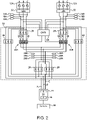
- FIG. 2 An example of a three-phase static transfer switch 10 is shown in Figure 2 .
- static transfer switches 10 are designed to complete a switching event between the two power sources 12A, 12B within one electrical cycle of the power sources 12A, 12B. This is desirable so that a high-quality, constant power supply is provided with minimal effect on the electrical load 14, 30.
- solid-state switches 22A, 22B first switches 22A and second switches 22B
- the switches 22A, 22B are silicon controlled rectifiers (SCR).
- thyristors may be used for the solid-state switches 22A, 22B, such as integrated gate-commutated thyristors (IGCT), reverse blocking integrated gate-commutated thyristors (RB-IGCT), or gate turn-off thyristors (GTO).
- IGCT integrated gate-commutated thyristors
- RB-IGCT reverse blocking integrated gate-commutated thyristors
- GTO gate turn-off thyristors
- each of the main switches 22A, 22B will be made up of multiple individual switches 26, with at least one switch 26 for each phase A, B, C.
- a pair of anti-parallel thyristors 26 is particularly well-suited for each switch 26 associated with a phase A, B, C.
- each switch 26 typically includes two switches 26A, 26B in an anti-parallel arrangement. However, each pair of anti-parallel thyristors 26A, 26B are often treated as a single switch 26 because they typically turn on and off together.
- the static transfer switch 10 may also include a series of manual switches 28 that are primarily used during maintenance to isolate sections of the circuit.
- first and/or second power sources 12A, 12B prefferably include an uninterruptible power supply (UPS) 32 to provide control over the electrical properties of the original source 12A, 12B and manage power drops or losses in the original source 12A, 12B.
- UPS uninterruptible power supply
- the output is typically coupled to the transformer 16 of a PDU 14, and the final electrical load 30 is often racks of computer servers 30 in a data center.
- An improvement of the invention herein is that it uses a resonant turn off topology adjusted to force commutate a three-phase power system and is operated by an embedded digital processor controlling the signals with software intelligence and algorithms in order to achieve autonomy and make possible a sub-millisecond transfer switch.
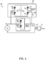
- the turn off circuit 40 with RTO topology is shown in Figure 3 .
- the circuit 40 includes a main circuit 42 and a resonant circuit 44.
- the main thyristors 26A, 26B (first switches) are S m1 and S m2 .
- the resonant circuit includes four auxiliary thyristor switches 34 (third switches) S r1 , S r2 , S r3 , S r4 , resonant capacitor C (energy storage) 36, and resonant inductor L 38.
- the capacitor C 36 is pre-charged to provide resonant current to create a zero-current crossing for the main thyristors 26.
- the inductor L 38 limits di/dt for main thyristors 26 during turn-off.
- main thyristors S m1 (or S m2 ) 26A, 26B are conducting and all the auxiliary switches 34 are off.
- the pre-charged resonant capacitor 36 is isolated from the main thyristor switches 26.
- the auxiliary switches 34 S r1,2 (or S r3,4 depending on current direction) are triggered to open by sending a gate signal thereto. As a result, the energy stored in the resonant capacitor 36 is discharged.
- the capacitor 36 voltage provides a negative bias voltage to help the main thyristor 26 turn off (i.e., open and stop conducting).
- the main thyristor 26 current reaches zero, it starts turning off with reverse bias voltage from the resonant capacitor 36.
- resonant capacitance value C pre-charged initial capacitor voltage V c0
- resonant inductance value L there are three possible design choices to control performance: resonant capacitance value C, pre-charged initial capacitor voltage V c0 , and resonant inductance value L. These parameters can be used to determine how much and how fast the main thyristor current can be turned off, as well as the size and cost of the auxiliary resonant circuit.
- Figure 4 shows the voltage and current waveforms of resonant turn-off operation for the main thyristors 26 and auxiliary switches 34.
- a gate signal is sent to turn off the main thyristor 26, and a gate signal is sent to turn on the auxiliary thyristors 34. This occurs as a result of degraded performance being identified by a sensor 18, 20.
- the second switches 22B cannot be closed to switch power to the second power source 12B until the first switches 22A have been opened, it would be beneficial to be able to stop current conduction through the first switches 22A faster than in a conventional static transfer switch.
- the resonance starts and the resonant current through L 38 increases fast.
- the main thyristor 26 current decreases to zero and starts turning off.
- the load 14, 16 current is commutated or bypassed to the auxiliary circuit 44 (34, 36, 38).
- the resonant capacitor 36 is re-charged by the load 14, 16 current but in reversed voltage polarity.
- the auxiliary thyristors 34 are turned off. As a result, the RTO has disconnected the first power source 12A and the load 14, 16 is ready to be transferred to the alternative power source 12B.
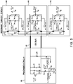
- the resonant circuits 44 (one for each phase) are shown in Figure 5 .
- a pre-charge circuit 46 is coupled to the resonant circuits 44 with a DC bus 48.
- the DC bus 48 is pre-charged slowly through the single bridge rectifier diodes 50 with resistors 52 to make sure capacitive inrush is prevented.
- a bleeding resistor 54 can be used to adjust that DC level to the desired value.
- a pre-charge relay 56 and bleed relay 58 are used to turn on and off the pre-charging and bleeding.
- a fourth switch 60 is provided between the pre-charge circuit 46 and the capacitors 36 to disconnect the pre-charge circuit 46 from the capacitors. The fourth switch 60 is preferably opened to stop charging of the capacitors in response to the switching event. If desired, fourth switches 60 may be provided for each resonant circuit 44 to disconnect the respective circuit 44 from the DC bus 48.
- a phase locked loop (PLL) 62 (see Figure 9 ) is used to determine the frequency and phase angle of the AC waveform of the power source 12A.
- the PLL 62 can be used in determining the firing sequence for the auxiliary switches 34 because the switches 34 need to be fired at the correct polarity. Since this is a three-phase system, the polarity of phase A, phase B and phase C will not be the same at the same time.
- the firing sequence is determined by the following algorithm:
- auxiliary switches 34 are turned on to release current from the capacitor 36, with one switch 34 being coupled to the input of the main thyristors 26 and the other switch 34 being coupled to the output of the main thyristors 26.
- the two auxiliary switches 34 that are turned on depends on current flow of the AC current through the main switches 26. Thus, when the current is positive, one pair of switches 34 will be turned on (while the other pair remains off), and when the current is negative, the other pair of switches 34 will be turned on (again, with the other pair remaining off).
- all of the main switches 22A, 26 are turned off (i.e., opened) and the auxiliary switches 34 are turned on (i.e., closed) at the same time in the static transfer switch 10. Because some phases A, B, C will have a positive current and some phases A, B, C will have a negative current at the switching instant, the pair of auxiliary switches 34 that is closed in each phase resonant circuit 44 will vary depending on the current of the particular phase A, B, C.
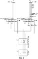
- the main circuits 42 are shown in Figure 6 .
- the table below lists the names of the signals used in the main circuits 42 and the resonant circuits 44 of Figures 5-6 .
- a DSP 64 ( Figures 2 and 8-9 ) may be used to generate the control signals used by the main circuits 42 and resonant circuits 44.
- FIG. 7 shows a flowchart of the method of transferring the power supply for the load 14 from one power source 12A to another power source 12B in a static transfer switch 10.
- the method may be implemented by a controller 64, which may be in the form of a DSP 64.
- steps 66-68 the energy storage (capacitors 36) are precharged by the charging circuit 46.
- the voltage of the DC bus 48 between the charging circuit 46 and the resonant circuits 44 is monitored and controlled to maintain a desired charge on the capacitors 36. That is, the relays 56, 58 are opened and closed as needed to supply voltage and bleed voltage to charge the capacitors 36.
- the quality of the power being supplied by the power source 12A connected to the load 14 is monitored for degraded performance events.
- the main switches 26 for the first power source 12A are opened to disconnect the first power source 12A from the load 14 in steps 72-78. That is, in step 72 turn off gate signals are sent to the main switches 26.
- the auxiliary switches 34 that must be turned on in each resonant circuit 44 are then determined in step 74 by phase locked loops 62 (see OUT_RTO_MINUS, OUT_RTO_PLUS algorithm above).
- the auxiliary switches 34 that have been determined in step 74 are then turned on with gate signals in step 76.
- step 78 the DSP 64 verifies that the preferred power source 12A is completely disconnected by confirming that the net value of the current and voltage passing through the main switches 22A, 26 for each phase of the preferred power source 12A is zero or negligible enough to confirm that the resonant circuits 44 did in fact reverse the bias for each of the main circuits 42.
- the DSP 64 can initiate a turn on command to the alternate power source 12B in step 80. Due to power quality considerations like inrush and soft start and preferred turn on conditions, it is possible to vary the method used to turn on the second power source 12B while still making use of the improved method of turning off the main switches 26 of the first power source 12A. After the main switches 22B, 26 for the alternate power source 12 have been turned on, the power transfer has been completed in step 82.
- FIGS 8-9 show a control system that may be used to control the resonant circuits 44, and associated charging circuit 46. It is understood that the control system may also be used to control the main circuits 42 as well.
- the Digital Signal Processor (DSP) 64 may be used to control all the relays, sense the voltages for the PLL synchronization and control the main switches 26, 42 and RTO thyristors 34, 44.
- a scaling processor 84 may be provided to adjust the inputs for use by the DSP 64.
- the DSP 64 may include a PLL element 62 and a phase decoder element 86 to evaluate the current direction of each phase and generate the gate signals for the auxiliary switches 34.
- Static transfer switches 10 are designed to transfer power to a load 14 between a preferred electrical power source 12A and alternate electrical power source 12B in response to power source quality disturbances.
- thyristors 26 are commonly used in conventional static transfer switches 10 due to their high current handling capability.
- thyristors 26 cannot be turned off by simply removing the gate signal to the thyristor 26, because a thyristor 26 is turned off when the conduction current through the thyristor 26 commutates below its minimum holding current (usually less than 1A) or the voltage applied to the thyristor 26 is reversed, which can be as long as half a cycle of the power source 12 fundamental frequency (e.g., 8.3 ms in 60 Hz AC systems).
- a resonant turn off (RTO) circuit 44 may be used as described above and below, where the resonant turn off circuit 44 is added in parallel to the thyristors 26.
- each phase A, B, C of each power source 12 has an individual resonant turn off circuit 44 in order to quickly turn off each phase during a transfer and to allow quick transfers back-and-forth in both directions between the power sources 12.
- six resonant turn off circuits 44 are required in for a two source static transfer switch 10.
- nine resonant turn off circuits 44 would be needed in a three source static transfer switch 10.
- the number of resonant turn off circuits 44 may be reduced by sharing the resonant turn off circuit 44 between the phases A, B, C of different power sources 12A, 12B. This may be useful in reducing the cost and complexity of the static transfer switch 10.
- an AC contactor or relay 90 may be used to select which power source 12A, 12B the resonant turn off circuit 44 is connected to.
- switches 90 i.e., a fourth and fifth switch
- an electro-mechanical switch 90 may be preferred due to the low cost, high capacity and reliability of such switches.
- contactors 20 with slower switching times than the main thyristors 26A and/or the auxiliary thyristors 34 may be used.
- individual contactors 90A, 90B may be used, with each contactor 90A, 90B corresponding to one of the power sources 12A, 12B and one of the phases A, B, C, a single double throw switch 90 as shown in Figure 10A may incorporate two switches 90A, 90B (i.e., the fourth and fifth switch) into one physical switch 90.
- the contactors 90A, 90B connect the shared resonant turn off circuit 44 to the main circuit 42 of the power source 12A, 12B that is currently supplying power to the electrical load 14.
- the resonant turn off circuit 44 is connected to and prepared to quickly turn off current through the operating main circuit 42 when a power transfer switching event is initiated. For example, when the thyristors 26 of the first power source 12A are closed such that power is being supplied from the first power source 12A to the load 14, the first contactors 90A are closed to connect the shared resonant turn off circuits 44 to the first thyristors 26 and the second contactors 90B are open to disconnect the shared resonant turn off circuits 44 from the second thyristors 26.
- the second contactors 90B are closed to connect the shared resonant turn off circuits 44 to the second thyristors 26 and the first contactors 90A are open to disconnect the shared resonant turn off circuits 44 from the second thyristors 26.
- the number of resonant turn off circuits 44 can be reduced to three instead of six as required in a conventional two source static transfer switch 10.
- the number of resonant turn off circuits 44 could be reduced from nine to three.
- the contactors 90 may also be useful in protecting the resonant turn off circuits 44 and/or isolating the circuits 44 during fault conditions (e.g., thyristor 26, 34 or IGBT 96 failures).
- the number of resonant turn off circuits 44 may also be reduced by eliminating the resonant turn off circuits 44 from one phase C of a three phase system.
- resonant turn off circuits 44 may be directly connected to the main circuits 42 of two of the phases A, B. In this arrangement, when the two main circuits 42 are turned off with the respective resonant turn off circuits 44, current flow from the third phase C is also forced to zero automatically through the delta input side 92 of the transformer 16 between the main circuits 42 and the electrical load 14.
- the resonant turn off circuits 44 directly connected to the main circuits 42 for phases 12A-A and 12A-B (i.e., phases A & B of source 12A) are activated. This causes the respective main circuits 42 to open and phases 12A-A and 12A-B to be disconnected from the load 14.
- One or both of the two resonant turn off circuits 44 then force the remaining main circuit 42 for phase 12A-C to open through the delta side 92 of the transformer 14 which disconnect the remaining main circuit 42 from the load 14.
- the third phase C may not have its own resonant turn off circuit 44, the current released by the two resonant turn off circuits 44 and the current conducted by all three main circuits 42 may cease flowing to the transformer 16 within 0.5 ms of the gate signals sent to the main circuits 42 or within less than half a cycle of the power source 12.
- the main circuits 42 for phases 12B-A, 12B-B, 12B-C are then closed to connect the second power source 12B to the load 14.
- the two resonant turn off circuits 44 are activated at the same time by closing the corresponding auxiliary switches 34 at the same time such that current from both resonant turn off circuits 44 forces the remaining main circuit 42 to open through the delta side 92 of the transformer 16.
- the output side of the transformer 16 is a wye side output 94.
- the present embodiment may be used to eliminate the resonant turn off circuit 44 from one of the phases C such that no resonant turn off circuit 44 is directly connected to the main circuit 42 of one phase C.
- the delta connected resonant turn off circuits 44 the number of resonant turn off circuits 44 can be reduced to four instead of six as required in a conventional two source static transfer switch 10.
- the number of resonant turn off circuits 44 could be reduced from nine to six.
- the designs of Figures 10 and 12 may also be combined to reduce the number of resonant turn off circuits 44 even further.
- the static transfer switch 10 may have shared resonant transfer circuits 44 between two corresponding phases A, B of the power sources 12A, B and may have one phase C connected through the delta side 92 of the transformer 16 that does not have its own resonant transfer circuit 44.
- the number of resonant turn off circuits 44 may be reduced from six to two in a two source system and from nine to two in a three source system.
- the operation of the resonant turn off circuit 44 of Figure 11 is illustrated in Figures 14A-E (refer to Figure 11 for detailed reference numbers), and the voltage and current is shown in Figure 15 . It is understood, however, that any type of resonant turn off circuit 44 may be used including the resonant turn off circuit 44 of Figures 3 and 5 .
- the capacitor 36 may be pre-charged to a relatively low voltage (40-50 V) and provides a resonant current to create a zero-current crossing for main circuit 42.
- a pre-charge circuit 46 may be provided for pre-charging the capacitor 36.
- the resonant inductor 38 limits the change in current to provide a softer commutation.
- the main thyristors 26 conduct current to the load 14.
- the gate signal to at least one of the main thyristors 42 is turned off, depending on the load current direction, and the corresponding auxiliary thyristors 34 and the IGBT 96 are closed with a gate signal.
- Sm1 conducts the load current.
- load current is forced to commutate from the main thyristor 26 to the resonant turn off circuit 44.
Landscapes
- Engineering & Computer Science (AREA)
- Power Engineering (AREA)
- Business, Economics & Management (AREA)
- Emergency Management (AREA)
- Stand-By Power Supply Arrangements (AREA)
- Inverter Devices (AREA)
- Dc-Dc Converters (AREA)
- Measurement Of Resistance Or Impedance (AREA)
- Electronic Switches (AREA)
Abstract
Description
- The present inventions relate generally to a static transfer switch for transferring power from one power source to another power source to supply an electrical load.
- Static transfer switches are used in the industry to control the electrical power supply to critical electrical components. In particular, static transfer switches are used for electrical loads like data centers where a constant, high-quality electrical supply is required.
- An example of a
static transfer switch 10 is shown inFigure 1 . As shown, two differentelectrical power sources static transfer switch 10. The output of thestatic transfer switch 10 is coupled to anelectrical load 14. Typically, the output is directly connected to a Power Distribution Unit (PDU) 14, which includes atransformer 16. The final electrical load may be racks of computer servers 30 (Figure 2 ) in a data center. However, it is understood thatstatic transfer switches 10 may also be used to supply power to other types of electrical loads. - The
static transfer switch 10 may include a variety ofsensors second power sources voltage power sources voltage 20B of the output. Thestatic transfer switch 10 also includes one ormore switches power sources static transfer switch 10 to supply power to the output from either of thepower sources first power source 12A may be thepreferred power source 12A (e.g., the grid), and thesecond power source 12B may be abackup power source 12B (e.g., a generator). In normal use, power can be supplied from thefirst power source 12A to theload 14 by closing thefirst switch 22A and opening thesecond switch 22B (to disconnect thesecond power source 12B). In the event that thefirst power source 12A suffers from degraded performance (e.g., drop in voltage) as determined from one or more of thesensors second power source 12B by opening thefirst switch 22A and closing thesecond switch 22B. Thus, theelectrical load 14 is provided with a constant source of power despite the possibility of degraded performance events in one of thepower sources - A static transfer switch is described for increasing the speed of switching from one power source to another power source. The system senses degraded performance of the power source supplying power to the load. In response to sensing degraded performance, the system turns off a gate signal to a first switch coupled between the power source and the load. The system also includes a resonant turn off circuit which forces the first switch to open during a switching event. The resonant turn off circuit is shared between the first switch associated with the first power source and a second switch associated with a second power source. The resonant turn off circuit can be selectively connected to either the first or second switch depending on which power source is supplying power to the load. The invention may also include any other aspect described below in the written description or in the attached drawings and any combinations thereof.
- According to an aspect, a static transfer switch is provided which comprises a first electrical power source, a second electrical power source, an electrical load, a first switch between the first electrical power source and the electrical load, a second switch between the second electrical power source and the electrical load, a resonant turn off circuit, a fourth switch between the resonant turn off circuit and the first switch, a fifth switch between the resonant turn off circuit and the second switch, wherein the fourth switch is closed to connect the resonant turn off circuit to the first switch when the first switch is closed and connecting the first electrical power source to the electrical load; and wherein the fifth switch is closed to connect the resonant turn off circuit to the second switch when the second switch is closed and connecting the second electrical power source to the electrical load.
- According to another embodiment, the fourth and fifth switches have slower switching times than the first and second switches.
- According to another embodiment, the fourth and fifth switches are electro-mechanical switches.
- According to another embodiment, the resonant turn off circuit comprises an energy storage and a third switch, the third switch being closed during a switching event to connect the energy storage to one of the first and second switches in order to force the one of the first and second switches to open.
- According to another embodiment, the third switch comprises a thyristor.
- According to another embodiment, the static transfer switch further comprises two of the third switch coupled to the first switch and the second switch, one of the third switches being coupled to the inputs of the first and second switches and another of the third switches being coupled to the outputs of the first and second switches, the energy storage being disposed between the two third switches.
- According to another embodiment, the static transfer switch further comprises two of the third switch coupled to the first switch and the second switch, the two third switches both being disposed between the energy storage and the inputs or the outputs of the first and second switches, wherein one of the two third switches is closed if a positive current is being conducted through the first or second switch and another of the two third switches is closed if a negative current is being conducted through the first or second switch.
- According to another embodiment, the static transfer switch further comprises four of the third switches coupled to the first switch and the second switch, two of the third switches being coupled to the inputs of the first and second switches and two of the third switches being coupled to the outputs of the first and second switches, the energy storage being disposed between two of the third switches on one side and two of the third switches on another side, wherein two of the third switches on opposite sides of the energy storage are closed if a positive current is being conducted through the first or second switch, and a different two of the third switches on opposite sides of the energy storage are closed if a negative current is being conducted through the first or second switch.
- According to another embodiment, the static transfer switch further comprises an inductor coupled between the inputs or outputs of the first and second switches and the third switch.
- According to another embodiment, the energy storage is a capacitor.
- According to another embodiment, the static transfer switch further comprises a charge circuit to maintain a predetermined charge of the energy storage.
- According to another embodiment, a current released by the resonant turn off circuit and a current conducted through the first switch and the second switch ceases to flow to the electrical load within 0.5 ms of turning off a gate signal to the first switch and the second switch during respective switching events.
- According to another embodiment, the fourth and fifth switches comprise a double throw switch.
- According to another embodiment, the resonant turn off circuit forces the first and second switches to open in less than one half an electrical cycle of the first and second electrical power sources, respectively.
- According to another embodiment, the first and second switches comprise silicon controlled rectifiers.
- According to another embodiment, the first and second switches comprise integrated gate-commutated thyristors (IGCT), reverse blocking integrated gate-commutated thyristors (IGCT), or gate turn-off thyristors (GTO).
- According to another embodiment, the static transfer switch further comprises a transformer between the first and second switches and the electrical load.
- According to another embodiment, the electrical load comprises a data center.
- According to another embodiment, one of the first and second electrical power sources comprises an uninterruptible power supply (UPS).
According to another aspect, a static transfer switch is provided which comprises a set of first power inputs coupled to a first three-phase electrical power source, each of the first power inputs being coupled to one phase of the first three-phase electrical power source, a set of second power inputs coupled to a second three-phase electrical power source, each of the second power inputs being coupled to one phase of the second three-phase electrical power source, a set of power outputs coupled to a three-phase electrical load, each of the power outputs being coupled to one phase of the three-phase electrical load, a set of first switches coupled between the set of first power inputs and the set of power outputs, a set of second switches coupled between the set of second power inputs and the set of power outputs, a set of third switches coupled between a set of energy storages and the set of first switches and between the set of energy storages and the set of second switches, each third switch being coupled between one of the energy storages and a respective first switch and a respective second switch, a set of fourth switches coupled between the set of third switches and the set of first switches, each fourth switch being coupled between a respective third switch and a respective first switch, a set of fifth switches coupled between the set of third switches and the set of second switches, each fifth switch being coupled between a respective third switch and a respective second switch, a sensor to determine an electrical property of the first three-phase electrical power source, a power transfer controller, the sensor being an input to the power transfer controller and the sets of first and second switches being outputs of the power transfer controller, wherein during normal operation the power transfer controller closes the set of first switches or the set of second switches to electrically connect the set of first power inputs or the set of second power inputs, respectively, to the set of power outputs and opens the other set of first switches or set of second switches to electrically disconnect the set of first power inputs or second power inputs, respectively, from the set of power outputs, the first three-phase electrical power source or the second three-phase electrical power source, respectively, thereby supplying power to the three-phase electrical load, wherein during normal operation the set of fourth switches remain closed and the fifth set of switches remain open when the first set of switches are closed and the fifth set of switches remain closed and the fourth set of switches remain open when the second set of switches are closed, wherein when the sensor identifies degraded performance of the first or second three-phase electrical power source connected to the three-phase electrical load, the power transfer controller initiates a switching event, comprising: turning off a gate signal to each of the first switches or the second switches which are closed during normal operation; closing at least one third switch between each first and second switches and each respective energy storage after the gate signal of the respective first switch or second switch has been turned off, the set of energy storages thereby releasing a current to the input or output of the respective first switch or second switch to force a drop in current conducted through the respective first switch or second switch, the drop in current causing the respective first switch or second switch to open and stop conducting current therethrough between the respective first or second three-phase electrical power source and the three-phase electrical load; closing the other set of first or second switches to supply power from the other of the first or second three-phase electrical power source to the three-phase electrical load; and after the first and second set of switches are opened and closed, opening the set of fourth switches and closing the set of fifth switches when the first set switches are opened and the second set of switches are closed during the switching event, and opening the set of fifth switches and closing the set of fourth switches when the second set switches are opened and the first set of switches are closed during the switching event. - The invention may be more fully understood by reading the following description in conjunction with the drawings, in which:
-
Figure 1 is a schematic of a static transfer switch; -
Figure 2 is a schematic of the static transfer switch showing three-phase power sources and a three-phase load; -
Figure 3 is a schematic of a switch circuit coupled between one phase of the power source and the load; -
Figure 4 is a series of graphs showing electrical properties of the switch circuit during opening of the switch between the power source and the load; -
Figure 5 is a schematic of a charge circuit for the energy storages; -
Figure 6 is another schematic of the static transfer switch; -
Figure 7 is a flow chart showing a transfer of power from one power source to another power source to supply a load; -
Figure 8 is a schematic of a digital signal processor used for controlling power through the static transfer switch; -
Figure 9 is another schematic of a digital signal processor used for controlling power through the static transfer switch; -
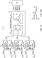
Figure 10 is another schematic of a static transfer switch; -
Figure 10A is a schematic of a double throw switch; -
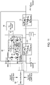
Figure 11 is a schematic of a resonant turn off circuit shared between two main circuits; -
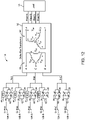
Figure 12 is another schematic of a static transfer switch; -
Figure 13 is another schematic of a static transfer switch; -
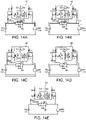
Figures 14A-E are schematics of the operation of a resonant turn off circuit; and -
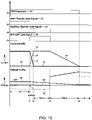
Figure 15 is a series of graphs showing electrical properties of the switch circuit ofFigures 14A-E . - An example of a three-phase
static transfer switch 10 is shown inFigure 2 . Typically, static transfer switches 10 are designed to complete a switching event between the twopower sources power sources electrical load state switches first switches 22A andsecond switches 22B) to perform the switching event since solid-state switches switches state switches static transfer switch 10, each of themain switches individual switches 26, with at least oneswitch 26 for each phase A, B, C. A pair ofanti-parallel thyristors 26 is particularly well-suited for eachswitch 26 associated with a phase A, B, C. Because thepower sources switch 26 typically includes twoswitches anti-parallel thyristors single switch 26 because they typically turn on and off together. Thestatic transfer switch 10 may also include a series ofmanual switches 28 that are primarily used during maintenance to isolate sections of the circuit. - It is often preferred for the first and/or
second power sources original source original source transformer 16 of aPDU 14, and the finalelectrical load 30 is often racks ofcomputer servers 30 in a data center. - An improvement of the invention herein is that it uses a resonant turn off topology adjusted to force commutate a three-phase power system and is operated by an embedded digital processor controlling the signals with software intelligence and algorithms in order to achieve autonomy and make possible a sub-millisecond transfer switch.
- The turn off
circuit 40 with RTO topology is shown inFigure 3 . As shown, thecircuit 40 includes amain circuit 42 and aresonant circuit 44. Themain thyristors resonant inductor L 38. Thecapacitor C 36 is pre-charged to provide resonant current to create a zero-current crossing for themain thyristors 26. Theinductor L 38 limits di/dt formain thyristors 26 during turn-off. During normal conduction, only the main thyristors Sm1 (or Sm2) 26A, 26B are conducting and all theauxiliary switches 34 are off. Thus, the pre-chargedresonant capacitor 36 is isolated from the main thyristor switches 26. In resonant turn-off operation, the auxiliary switches 34 Sr1,2 (or Sr3,4 depending on current direction) are triggered to open by sending a gate signal thereto. As a result, the energy stored in theresonant capacitor 36 is discharged. When the resonant current through the inductor 38 L exceeds the load current, the current through themain thyristor 26 is commuted to the resonant circuit. In the meantime, thecapacitor 36 voltage provides a negative bias voltage to help themain thyristor 26 turn off (i.e., open and stop conducting). When themain thyristor 26 current reaches zero, it starts turning off with reverse bias voltage from theresonant capacitor 36. In the RTO topology, there are three possible design choices to control performance: resonant capacitance value C, pre-charged initial capacitor voltage V c0, and resonant inductance value L. These parameters can be used to determine how much and how fast the main thyristor current can be turned off, as well as the size and cost of the auxiliary resonant circuit. -
Figure 4 shows the voltage and current waveforms of resonant turn-off operation for themain thyristors 26 and auxiliary switches 34. As shown in the bottom graph, at time 0.1 seconds a gate signal is sent to turn off themain thyristor 26, and a gate signal is sent to turn on theauxiliary thyristors 34. This occurs as a result of degraded performance being identified by a sensor 18, 20. Because thesecond switches 22B cannot be closed to switch power to thesecond power source 12B until thefirst switches 22A have been opened, it would be beneficial to be able to stop current conduction through thefirst switches 22A faster than in a conventional static transfer switch. That is, once a turn on gate signal has been applied to an SCR, current will continue to be conducted through the SCR even after a turn off gate signal is applied. However, after a turn off gate signal is applied to the SCR, the SCR will stop conducting current after the current drops below a threshold. That normally occurs with an AC current when the current waveform crosses zero. However, that may require up to half of an AC cycle for the power source waveform to cross zero (i.e., 8 ms). It would be beneficial to be able to stop thefirst switches 26A quicker so that the second switches can be closed more quickly to transfer power as quick as possible from thefirst power source 12A to thesecond power source 12B. As shown in the top graph inFigure 4 , current to theload auxiliary thyristors auxiliary thyristors - Referring to
Figure 4 , after the auxiliaryresonant thyristors 34 are triggered, the resonance starts and the resonant current throughL 38 increases fast. Once the resonant current is larger than theload main thyristor 26 current decreases to zero and starts turning off. In the meanwhile, theload resonant capacitor 36 is re-charged by theload resonant capacitor 36 voltage is high enough and theload auxiliary thyristors 34 are turned off. As a result, the RTO has disconnected thefirst power source 12A and theload alternative power source 12B. - The resonant circuits 44 (one for each phase) are shown in
Figure 5 . As shown, apre-charge circuit 46 is coupled to theresonant circuits 44 with aDC bus 48. Preferably, theDC bus 48 is pre-charged slowly through the singlebridge rectifier diodes 50 withresistors 52 to make sure capacitive inrush is prevented. Also, in case theDC bus 48 runs above the set limit, a bleedingresistor 54 can be used to adjust that DC level to the desired value. Apre-charge relay 56 and bleedrelay 58 are used to turn on and off the pre-charging and bleeding. Preferably, afourth switch 60 is provided between thepre-charge circuit 46 and thecapacitors 36 to disconnect thepre-charge circuit 46 from the capacitors. Thefourth switch 60 is preferably opened to stop charging of the capacitors in response to the switching event. If desired,fourth switches 60 may be provided for eachresonant circuit 44 to disconnect therespective circuit 44 from theDC bus 48. - A phase locked loop (PLL) 62 (see
Figure 9 ) is used to determine the frequency and phase angle of the AC waveform of thepower source 12A. ThePLL 62 can be used in determining the firing sequence for theauxiliary switches 34 because theswitches 34 need to be fired at the correct polarity. Since this is a three-phase system, the polarity of phase A, phase B and phase C will not be the same at the same time. The firing sequence is determined by the following algorithm:

- The same algorithm is applied for the other remaining phases to complete the firing sequence in case a transfer is needed. In other words, only two of the
auxiliary switches 34 are turned on to release current from thecapacitor 36, with oneswitch 34 being coupled to the input of themain thyristors 26 and theother switch 34 being coupled to the output of themain thyristors 26. The twoauxiliary switches 34 that are turned on depends on current flow of the AC current through the main switches 26. Thus, when the current is positive, one pair ofswitches 34 will be turned on (while the other pair remains off), and when the current is negative, the other pair ofswitches 34 will be turned on (again, with the other pair remaining off). Preferably, all of themain switches auxiliary switches 34 are turned on (i.e., closed) at the same time in thestatic transfer switch 10. Because some phases A, B, C will have a positive current and some phases A, B, C will have a negative current at the switching instant, the pair ofauxiliary switches 34 that is closed in each phaseresonant circuit 44 will vary depending on the current of the particular phase A, B, C. - The
main circuits 42 are shown inFigure 6 . The table below lists the names of the signals used in themain circuits 42 and theresonant circuits 44 ofFigures 5-6 . As explained below, a DSP 64 (Figures 2 and8-9 ) may be used to generate the control signals used by themain circuits 42 andresonant circuits 44.Name Function Description INPUT_AC_A Input Phase A voltage sensing for PLL INPUT_AC_B Input Phase B voltage sensing for PLL INPUT_AC_C Input Phase C voltage sensing for PLL IN_DC Input Bus voltage for the capacitor OUT_RTO_PLUS_A Output Phase A positive RTO OUT_RTO_MINUS_A Output Phase A negative RTO OUT_RTO_PLUS_B Output Phase B positive RTO OUT_RTO_MINUS_B Output Phase B negative RTO OUT_RTO_PLUS_C Output Phase C positive RTO OUT_RTO_MINUS_C Output Phase C negative RTO OUT_PRECHARGE Output Pre-charge relay control signal OUT_BLEEDER Output Bleeder relay control signal OUT_SCR_PREFERRED Output Preferred side SCR gating signal OUT_SCR_ALTERNATE Output Alternate side SCR gating signal -
Figure 7 shows a flowchart of the method of transferring the power supply for theload 14 from onepower source 12A to anotherpower source 12B in astatic transfer switch 10. As understood, the method may be implemented by acontroller 64, which may be in the form of aDSP 64. In steps 66-68, the energy storage (capacitors 36) are precharged by the chargingcircuit 46. The voltage of theDC bus 48 between the chargingcircuit 46 and theresonant circuits 44 is monitored and controlled to maintain a desired charge on thecapacitors 36. That is, therelays capacitors 36. Instep 70, the quality of the power being supplied by thepower source 12A connected to theload 14 is monitored for degraded performance events. When such a situation is identified, themain switches 26 for thefirst power source 12A are opened to disconnect thefirst power source 12A from theload 14 in steps 72-78. That is, instep 72 turn off gate signals are sent to the main switches 26. The auxiliary switches 34 that must be turned on in eachresonant circuit 44 are then determined instep 74 by phase locked loops 62 (see OUT_RTO_MINUS, OUT_RTO_PLUS algorithm above). The auxiliary switches 34 that have been determined instep 74 are then turned on with gate signals instep 76. - In
step 78, theDSP 64 verifies that the preferredpower source 12A is completely disconnected by confirming that the net value of the current and voltage passing through themain switches power source 12A is zero or negligible enough to confirm that theresonant circuits 44 did in fact reverse the bias for each of themain circuits 42. Finally, theDSP 64 can initiate a turn on command to thealternate power source 12B instep 80. Due to power quality considerations like inrush and soft start and preferred turn on conditions, it is possible to vary the method used to turn on thesecond power source 12B while still making use of the improved method of turning off themain switches 26 of thefirst power source 12A. After themain switches alternate power source 12 have been turned on, the power transfer has been completed instep 82. -
Figures 8-9 show a control system that may be used to control theresonant circuits 44, and associated chargingcircuit 46. It is understood that the control system may also be used to control themain circuits 42 as well. The Digital Signal Processor (DSP) 64 may be used to control all the relays, sense the voltages for the PLL synchronization and control themain switches RTO thyristors processor 84 may be provided to adjust the inputs for use by theDSP 64. As also shown inFigure 9 , theDSP 64 may include aPLL element 62 and aphase decoder element 86 to evaluate the current direction of each phase and generate the gate signals for the auxiliary switches 34. - Static transfer switches 10 are designed to transfer power to a
load 14 between a preferredelectrical power source 12A and alternateelectrical power source 12B in response to power source quality disturbances. Traditionally, thyristors 26 are commonly used in conventional static transfer switches 10 due to their high current handling capability. As a semi-controlled device,thyristors 26 cannot be turned off by simply removing the gate signal to thethyristor 26, because athyristor 26 is turned off when the conduction current through thethyristor 26 commutates below its minimum holding current (usually less than 1A) or the voltage applied to thethyristor 26 is reversed, which can be as long as half a cycle of thepower source 12 fundamental frequency (e.g., 8.3 ms in 60 Hz AC systems). To speed up commutation of thethyristors 26, a resonant turn off (RTO)circuit 44 may be used as described above and below, where the resonant turn offcircuit 44 is added in parallel to thethyristors 26. Duringthyristor 26 turn-off, a reverse current is injected by the resonant turn offcircuit 44 to force thethyristor 26 current to commutate quickly to zero. In this way, the resonant turn offcircuit 44 can interrupt the current within 1 ms, or preferably less than a half cycle of thepower sources 12, which greatly shortens the disconnect time of the off goingelectrical power source 12. Typically, each phase A, B, C of eachpower source 12 has an individual resonant turn offcircuit 44 in order to quickly turn off each phase during a transfer and to allow quick transfers back-and-forth in both directions between thepower sources 12. Thus, six resonant turn offcircuits 44 are required in for a two sourcestatic transfer switch 10. Likewise, nine resonant turn offcircuits 44 would be needed in a three sourcestatic transfer switch 10. - As shown in
Figures 10-11 , the number of resonant turn offcircuits 44 may be reduced by sharing the resonant turn offcircuit 44 between the phases A, B, C ofdifferent power sources static transfer switch 10. As shown, an AC contactor or relay 90 may be used to select whichpower source circuit 44 is connected to. Various types of switches 90 (i.e., a fourth and fifth switch) may be used to connect the resonant turn offcircuit 44 to a selectedpower source mechanical switch 90 may be preferred due to the low cost, high capacity and reliability of such switches. Since the switching times of thecontactors 90 is not critical because thecontactors 90 are not directly involved in the actual switching event of turning off thethyristors 26A of onesource 12A and turning on thethyristors 26B of theother source 12B, contactors 20 with slower switching times than themain thyristors 26A and/or theauxiliary thyristors 34 may be used. Althoughindividual contactors contactor power sources double throw switch 90 as shown inFigure 10A may incorporate twoswitches physical switch 90. In use, thecontactors circuit 44 to themain circuit 42 of thepower source electrical load 14. As a result, the resonant turn offcircuit 44 is connected to and prepared to quickly turn off current through the operatingmain circuit 42 when a power transfer switching event is initiated. For example, when thethyristors 26 of thefirst power source 12A are closed such that power is being supplied from thefirst power source 12A to theload 14, thefirst contactors 90A are closed to connect the shared resonant turn offcircuits 44 to thefirst thyristors 26 and thesecond contactors 90B are open to disconnect the shared resonant turn offcircuits 44 from thesecond thyristors 26. Conversely, when thethyristors 26 of thesecond power source 12B are closed such that power is being supplied from thesecond power source 12B to theload 14, thesecond contactors 90B are closed to connect the shared resonant turn offcircuits 44 to thesecond thyristors 26 and thefirst contactors 90A are open to disconnect the shared resonant turn offcircuits 44 from thesecond thyristors 26. As a result of the shared arrangement of the resonant turn offcircuits 44, the number of resonant turn offcircuits 44 can be reduced to three instead of six as required in a conventional two sourcestatic transfer switch 10. Similarly, in a three source system, the number of resonant turn offcircuits 44 could be reduced from nine to three. Thecontactors 90 may also be useful in protecting the resonant turn offcircuits 44 and/or isolating thecircuits 44 during fault conditions (e.g.,thyristor IGBT 96 failures). - As shown in
Figure 12 , the number of resonant turn offcircuits 44 may also be reduced by eliminating the resonant turn offcircuits 44 from one phase C of a three phase system. Thus, as shown resonant turn offcircuits 44 may be directly connected to themain circuits 42 of two of the phases A, B. In this arrangement, when the twomain circuits 42 are turned off with the respective resonant turn offcircuits 44, current flow from the third phase C is also forced to zero automatically through thedelta input side 92 of thetransformer 16 between themain circuits 42 and theelectrical load 14. For example, in a power transfer switching event where power is initially being supplied by thefirst power source 12A, the resonant turn offcircuits 44 directly connected to themain circuits 42 forphases 12A-A and 12A-B (i.e., phases A & B ofsource 12A) are activated. This causes the respectivemain circuits 42 to open and phases 12A-A and 12A-B to be disconnected from theload 14. One or both of the two resonant turn offcircuits 44 then force the remainingmain circuit 42 forphase 12A-C to open through thedelta side 92 of thetransformer 14 which disconnect the remainingmain circuit 42 from theload 14. Even though the third phase C may not have its own resonant turn offcircuit 44, the current released by the two resonant turn offcircuits 44 and the current conducted by all threemain circuits 42 may cease flowing to thetransformer 16 within 0.5 ms of the gate signals sent to themain circuits 42 or within less than half a cycle of thepower source 12. Themain circuits 42 forphases 12B-A, 12B-B, 12B-C are then closed to connect thesecond power source 12B to theload 14. Preferably, the two resonant turn offcircuits 44 are activated at the same time by closing the correspondingauxiliary switches 34 at the same time such that current from both resonant turn offcircuits 44 forces the remainingmain circuit 42 to open through thedelta side 92 of thetransformer 16. Preferably, the output side of thetransformer 16 is awye side output 94. Thus, whereas a conventionalstatic transfer switch 10 would have a separate resonant turn offcircuit 44 for each phase A, B, C of a three-phaseelectrical power source 12, the present embodiment may be used to eliminate the resonant turn offcircuit 44 from one of the phases C such that no resonant turn offcircuit 44 is directly connected to themain circuit 42 of one phase C. As a result of the delta connected resonant turn offcircuits 44, the number of resonant turn offcircuits 44 can be reduced to four instead of six as required in a conventional two sourcestatic transfer switch 10. Similarly, in a three source system, the number of resonant turn offcircuits 44 could be reduced from nine to six. - As shown in
Figure 13 , the designs ofFigures 10 and12 may also be combined to reduce the number of resonant turn offcircuits 44 even further. Thus, thestatic transfer switch 10 may have sharedresonant transfer circuits 44 between two corresponding phases A, B of thepower sources 12A, B and may have one phase C connected through thedelta side 92 of thetransformer 16 that does not have its ownresonant transfer circuit 44. As a result, the number of resonant turn offcircuits 44 may be reduced from six to two in a two source system and from nine to two in a three source system. - The operation of the resonant turn off
circuit 44 ofFigure 11 is illustrated inFigures 14A-E (refer toFigure 11 for detailed reference numbers), and the voltage and current is shown inFigure 15 . It is understood, however, that any type of resonant turn offcircuit 44 may be used including the resonant turn offcircuit 44 ofFigures 3 and5 . Thecapacitor 36 may be pre-charged to a relatively low voltage (40-50 V) and provides a resonant current to create a zero-current crossing formain circuit 42. Apre-charge circuit 46 may be provided for pre-charging thecapacitor 36. Theresonant inductor 38 limits the change in current to provide a softer commutation. As shown inFigure 14A , before t1, themain thyristors 26 conduct current to theload 14. InFigure 14B , at t1, when a switching event is initiated, the gate signal to at least one of themain thyristors 42 is turned off, depending on the load current direction, and the correspondingauxiliary thyristors 34 and theIGBT 96 are closed with a gate signal. For example, in Fig.4(a), Sm1 conducts the load current. From t1 to t2, inFigure 14B , load current is forced to commutate from themain thyristor 26 to the resonant turn offcircuit 44. InFigure 14C , at t2, reversed bias voltage from thecapacitor 36 is applied to the anode of themain thyristor 26 to speed up its turn-off. As shown inFigure 15 , thecapacitor 36 discharges and voltage of thecapacitor 36 drops during this period. The energy stored in thecapacitor 36 is preferably large enough to maintain the voltage polarity and reverse the bias to themain thyristor 26. The period between t2 and t3 allows sufficient time for themain thyristor 26 to commutate. InFigure 14D , at t3, themain thyristor 26 is completely blocks forward voltage, and theauxiliary thyristors 34 andIGBT 96 are commanded to turn-off. From t3 to t4, inFigure 14D , the voltage of theresonant capacitor 98 increases until reaching the clamping voltage. InFigure 14E , loop energy has been absorbed by thesnubber circuit 100, and the load current is zero and has been completely interrupted at t4. It is understood that a variety of resonant turn offcircuits 44 may be used herein, with additional examples being provided inU.S. Patent Application Serial No. 16/795,988 , which is incorporated by reference herein. - While preferred embodiments of the inventions have been described, it should be understood that the inventions are not so limited, and modifications may be made without departing from the inventions herein. While each embodiment described herein may refer only to certain features and may not specifically refer to every feature described with respect to other embodiments, it should be recognized that the features described herein are interchangeable unless described otherwise, even where no reference is made to a specific feature. It should also be understood that the advantages described above are not necessarily the only advantages of the inventions, and it is not necessarily expected that all of the described advantages will be achieved with every embodiment of the inventions. The scope of the inventions is defined by the appended claims, and all devices and methods that come within the meaning of the claims, either literally or by equivalence, are intended to be embraced therein.
Claims (17)
- A static transfer switch, comprising:a first electrical power source;a second electrical power source;an electrical load;a first switch between the first electrical power source and the electrical load;a second switch between the second electrical power source and the electrical load;a resonant turn off circuit;a fourth switch between the resonant turn off circuit and the first switch;a fifth switch between the resonant turn off circuit and the second switch;wherein the fourth switch is closed to connect the resonant turn off circuit to the first switch when the first switch is closed and connecting the first electrical power source to the electrical load; andwherein the fifth switch is closed to connect the resonant turn off circuit to the second switch when the second switch is closed and connecting the second electrical power source to the electrical load.
- The static transfer switch according to claim 1, wherein the fourth and fifth switches have slower switching times than the first and second switches; and/or wherein the fourth and fifth switches are electro-mechanical switches.
- The static transfer switch according to one of the preceding claims, wherein the resonant turn off circuit comprises an energy storage and a third switch, the third switch being closed during a switching event to connect the energy storage to one of the first and second switches in order to force the one of the first and second switches to open.
- The static transfer switch according to claim 3, wherein the third switch comprises a thyristor.
- The static transfer switch according to claim 3 or 4, further comprising two of the third switch coupled to the first switch and the second switch, one of the third switches being coupled to the inputs of the first and second switches and another of the third switches being coupled to the outputs of the first and second switches, the energy storage being disposed between the two third switches.
- The static transfer switch according to one of claims 3 to 5, further comprising two of the third switch coupled to the first switch and the second switch, the two third switches both being disposed between the energy storage and the inputs or the outputs of the first and second switches, wherein one of the two third switches is closed if a positive current is being conducted through the first or second switch and another of the two third switches is closed if a negative current is being conducted through the first or second switch.
- The static transfer switch according to one of claims 3 to 6, further comprising four of the third switches coupled to the first switch and the second switch, two of the third switches being coupled to the inputs of the first and second switches and two of the third switches being coupled to the outputs of the first and second switches, the energy storage being disposed between two of the third switches on one side and two of the third switches on another side, wherein two of the third switches on opposite sides of the energy storage are closed if a positive current is being conducted through the first or second switch, and a different two of the third switches on opposite sides of the energy storage are closed if a negative current is being conducted through the first or second switch.
- The static transfer switch according to one of claims 3 to 7, further comprising an inductor coupled between the inputs or outputs of the first and second switches and the third switch.
- The static transfer switch according to one of claims 3 to 8, wherein the energy storage is a capacitor.
- The static transfer switch according to one of claims 3 to 9, further comprising a charge circuit to maintain a predetermined charge of the energy storage.
- The static transfer switch according to one of the preceding claims, wherein a current released by the resonant turn off circuit and a current conducted through the first switch and the second switch ceases to flow to the electrical load within 0.5 ms of turning off a gate signal to the first switch and the second switch during respective switching events.
- The static transfer switch according to one of the preceding claims,wherein the fourth and fifth switches comprise a double throw switch; and/orwherein the first and second switches comprise silicon controlled rectifiers.
- The static transfer switch according to one of the preceding claims, wherein the resonant turn off circuit forces the first and second switches to open in less than one half an electrical cycle of the first and second electrical power sources, respectively.
- The static transfer switch according to one of the preceding claims, wherein the first and second switches comprise integrated gate-commutated thyristors (IGCT), reverse blocking integrated gate-commutated thyristors (IGCT), or gate turn-off thyristors (GTO).
- The static transfer switch according to one of the preceding claims, further comprising a transformer between the first and second switches and the electrical load; and/or
wherein the electrical load comprises a data center. - The static transfer switch according to one of the preceding claims, wherein one of the first and second electrical power sources comprises an uninterruptible power supply (UPS).
- A static transfer switch, comprising:a set of first power inputs coupled to a first three-phase electrical power source, each of the first power inputs being coupled to one phase of the first three-phase electrical power source;a set of second power inputs coupled to a second three-phase electrical power source, each of the second power inputs being coupled to one phase of the second three-phase electrical power source;a set of power outputs coupled to a three-phase electrical load, each of the power outputs being coupled to one phase of the three-phase electrical load;a set of first switches coupled between the set of first power inputs and the set of power outputs;a set of second switches coupled between the set of second power inputs and the set of power outputs;a set of third switches coupled between a set of energy storages and the set of first switches and between the set of energy storages and the set of second switches, each third switch being coupled between one of the energy storages and a respective first switch and a respective second switch;a set of fourth switches coupled between the set of third switches and the set of first switches, each fourth switch being coupled between a respective third switch and a respective first switch;a set of fifth switches coupled between the set of third switches and the set of second switches, each fifth switch being coupled between a respective third switch and a respective second switch;a sensor to determine an electrical property of the first three-phase electrical power source;a power transfer controller, the sensor being an input to the power transfer controller and the sets of first and second switches being outputs of the power transfer controller;wherein during normal operation the power transfer controller closes the set of first switches or the set of second switches to electrically connect the set of first power inputs or the set of second power inputs, respectively, to the set of power outputs and opens the other set of first switches or set of second switches to electrically disconnect the set of first power inputs or second power inputs, respectively, from the set of power outputs, the first three-phase electrical power source or the second three-phase electrical power source, respectively, thereby supplying power to the three-phase electrical load;wherein during normal operation the set of fourth switches remain closed and the fifth set of switches remain open when the first set of switches are closed and the fifth set of switches remain closed and the fourth set of switches remain open when the second set of switches are closed;wherein when the sensor identifies degraded performance of the first or second three-phase electrical power source connected to the three-phase electrical load, the power transfer controller initiates a switching event, comprising:turning off a gate signal to each of the first switches or the second switches which are closed during normal operation;closing at least one third switch between each first and second switches and each respective energy storage after the gate signal of the respective first switch or second switch has been turned off, the set of energy storages thereby releasing a current to the input or output of the respective first switch or second switch to force a drop in current conducted through the respective first switch or second switch, the drop in current causing the respective first switch or second switch to open and stop conducting current therethrough between the respective first or second three-phase electrical power source and the three-phase electrical load;closing the other set of first or second switches to supply power from the other of the first or second three-phase electrical power source to the three-phase electrical load; andafter the first and second set of switches are opened and closed, opening the set of fourth switches and closing the set of fifth switches when the first set switches are opened and the second set of switches are closed during the switching event, and opening the set of fifth switches and closing the set of fourth switches when the second set switches are opened and the first set of switches are closed during the switching event.
Applications Claiming Priority (1)
| Application Number | Priority Date | Filing Date | Title |
|---|---|---|---|
| US17/100,040 US11258296B1 (en) | 2020-11-20 | 2020-11-20 | Shared resonant turn off circuit |
Publications (1)
| Publication Number | Publication Date |
|---|---|
| EP4002693A1 true EP4002693A1 (en) | 2022-05-25 |
Family
ID=78789629
Family Applications (1)
| Application Number | Title | Priority Date | Filing Date |
|---|---|---|---|
| EP21208731.6A Pending EP4002693A1 (en) | 2020-11-20 | 2021-11-17 | Shared resonant turn off circuit used by several semiconductor switches |
Country Status (4)
| Country | Link |
|---|---|
| US (1) | US11258296B1 (en) |
| EP (1) | EP4002693A1 (en) |
| CN (1) | CN114552756B (en) |
| CA (1) | CA3139174C (en) |
Cited By (2)
| Publication number | Priority date | Publication date | Assignee | Title |
|---|---|---|---|---|
| EP4358336A3 (en) * | 2022-10-19 | 2024-10-23 | Abb Schweiz Ag | Convertible transfer switch |
| WO2025122718A1 (en) * | 2023-12-08 | 2025-06-12 | Abb Schweiz Ag | Switched redundant static transfer switch rapid turn-off system |
Families Citing this family (2)
| Publication number | Priority date | Publication date | Assignee | Title |
|---|---|---|---|---|
| US20250096551A1 (en) * | 2023-09-19 | 2025-03-20 | Abb Schweiz Ag | System and method for transfer switch utilizing recloser operations |
| US20250316982A1 (en) * | 2024-04-03 | 2025-10-09 | Abb Schweiz Ag | Dual mode power transfer switches |
Citations (3)
| Publication number | Priority date | Publication date | Assignee | Title |
|---|---|---|---|---|
| US3931563A (en) * | 1974-09-25 | 1976-01-06 | Westinghouse Electric Corporation | Force commutation static frequency changer apparatus using direct current chopper technique |
| US20180091137A1 (en) * | 2016-09-28 | 2018-03-29 | Rockwell Automation Technologies, Inc. | Auxiliary commutated silicon-controlled rectifier circuit methods and systems |
| US20200358309A1 (en) * | 2019-05-06 | 2020-11-12 | Vertiv Corporation | System and method for shared hybrid transfer switch |
Family Cites Families (42)
| Publication number | Priority date | Publication date | Assignee | Title |
|---|---|---|---|---|
| FR2396484A1 (en) | 1977-06-30 | 1979-01-26 | Telic | THYRISTOR SWITCHING MATRIX |
| US4210846A (en) | 1978-12-05 | 1980-07-01 | Lutron Electronics Co., Inc. | Inverter circuit for energizing and dimming gas discharge lamps |
| DE3123019A1 (en) | 1981-06-10 | 1983-01-05 | Siemens AG, 1000 Berlin und 8000 München | THYRISTOR ARRANGEMENT WITH AT LEAST FOUR THYRISTOR PILLARS |
| US5343140A (en) | 1992-12-02 | 1994-08-30 | Motorola, Inc. | Zero-voltage-switching quasi-resonant converters with multi-resonant bipolar switch |
| US5436786A (en) | 1992-12-21 | 1995-07-25 | Dairyland Electrical Industries, Inc. | Isolator surge protector for DC isolation and AC grounding of cathodically protected systems |
| US5694007A (en) | 1995-04-19 | 1997-12-02 | Systems And Services International, Inc. | Discharge lamp lighting system for avoiding high in-rush current |
| US5689164A (en) | 1995-12-08 | 1997-11-18 | Kabushiki Kaisha Toyoda Jidoshokki Seisakusho | Resonant power electronic control of switched reluctance motor |
| US5770897A (en) | 1996-09-16 | 1998-06-23 | Abb Power T&D Company Inc. | Hybrid solid state switch |
| US6118676A (en) | 1998-11-06 | 2000-09-12 | Soft Switching Technologies Corp. | Dynamic voltage sag correction |
| US6560128B1 (en) | 1999-02-12 | 2003-05-06 | Satcon Power Systems Canada Ltd. | Ferroresonance-suppressing static transfer switch |
| US6317346B1 (en) | 2000-11-09 | 2001-11-13 | At&T Corporation | Redundant multiphase power supplies for common load device |
| US7129599B2 (en) | 2002-10-15 | 2006-10-31 | Soft Switching Technologies Corporation | Dual feed power supply systems with enhanced power quality |
| US7459804B2 (en) | 2004-02-10 | 2008-12-02 | Liebert Corporation | Static transfer switch device and method |
| US7589438B2 (en) | 2004-07-09 | 2009-09-15 | Layerzero Power Systems, Inc. | Source phase sensitive transfer method and apparatus |
| US7265458B2 (en) | 2005-04-08 | 2007-09-04 | Eaton Power Quality Corporation | Apparatus and methods for coordinated static switch operations for load transfers in uninterruptible power supply systems |
| EP2132850A4 (en) | 2007-04-05 | 2012-04-11 | Georgia Tech Res Inst | PROTECTION AGAINST OVERVOLTAGE |
| KR101079900B1 (en) | 2007-10-31 | 2011-11-04 | 주식회사 케이티 | Static transfer switch device, power supply apparatus using the switch device and switching method thereof |
| GB0724369D0 (en) | 2007-12-13 | 2008-01-30 | Univ Aberdeen | Power converter |
| CN101540493B (en) | 2009-04-22 | 2011-01-19 | 南京航空航天大学 | Resonance type DC solid circuit breaker |
| CN101854075B (en) | 2010-05-27 | 2012-09-05 | Asco电力技术公司 | Arc extinguishing hybrid switch and switching method |
| GB201101672D0 (en) | 2011-01-31 | 2011-03-16 | Imp Innovations Ltd | Electrical devices with improved fault current handling capabilities |
| US8743565B2 (en) | 2012-07-27 | 2014-06-03 | Flextronics Ap, Llc | High power converter architecture |
| WO2014018967A1 (en) | 2012-07-27 | 2014-01-30 | Thoratec Corporation | Self-tuning resonant power transfer systems |
| US20140039711A1 (en) * | 2012-08-02 | 2014-02-06 | Varentec, Inc. | Dynamic source balancing methods and systems |
| CN102820699B (en) * | 2012-08-09 | 2014-06-11 | 常熟瑞特电气股份有限公司 | Intelligent digital static switch |
| US9362781B2 (en) | 2012-09-14 | 2016-06-07 | Chloride Srl | Uninterruptible power supply system with fast transfer for undervoltage source line failures |
| US9520874B2 (en) | 2012-11-09 | 2016-12-13 | Liebert Corporation | Operating a static transfer switch to eliminate transformer inrush current in the presence of residual flux |
| US20140254223A1 (en) | 2013-03-07 | 2014-09-11 | Rudolf Limpaecher | Method and system for a high speed soft-switching resonant converter |
| TW201438366A (en) | 2013-03-26 | 2014-10-01 | Li shu qi | Highly reliable static switching switch circuit for uninterruptable power system |
| GB201308051D0 (en) | 2013-05-03 | 2013-06-12 | Univ Manchester | Apparatus and method for controlling a DC current |
| EP3111546A1 (en) * | 2014-02-27 | 2017-01-04 | Danmarks Tekniske Universitet | On and off controlled resonant dc-dc power converter |
| JP6749319B2 (en) | 2014-06-30 | 2020-09-02 | サイブレーク アーベーScibreak Ab | Device, system and method for interrupting current |
| US9467112B2 (en) | 2014-07-25 | 2016-10-11 | Ge Energy Power Conversion Technology Ltd | Hybrid thyristor-controlled series capacitor and passive damping filter for series capacitors |
| US9899868B2 (en) | 2014-10-31 | 2018-02-20 | Ideal Power, Inc. | Smart transfer switch devices, systems, and methods using double-base bipolar transistors |
| US9479160B2 (en) | 2014-12-17 | 2016-10-25 | GlobalFoundries, Inc. | Resonant radio frequency switch |
| WO2016104623A1 (en) | 2014-12-26 | 2016-06-30 | 国立大学法人東京工業大学 | Circuit breaker |
| US9825489B2 (en) | 2015-01-26 | 2017-11-21 | Vertiv S.R.L. | Method of controlling an uninterruptible power supply to clear a shorted load |
| US10931190B2 (en) | 2015-10-22 | 2021-02-23 | Inertech Ip Llc | Systems and methods for mitigating harmonics in electrical systems by using active and passive filtering techniques |
| US11050250B2 (en) | 2015-10-30 | 2021-06-29 | Abb Schweiz Ag | Static transfer switch system with real time flux control |
| GB2566479B (en) * | 2017-09-14 | 2019-10-23 | Eltek As | DC-DC Converter |
| US10734834B2 (en) | 2018-06-04 | 2020-08-04 | Abb Schweiz Ag | Static transfer switch with resonant turn-off |
| CN209184310U (en) * | 2018-12-21 | 2019-07-30 | 青岛创统科技发展有限公司 | A kind of MW class static state switching switch and uninterruptible power supply |
-
2020
- 2020-11-20 US US17/100,040 patent/US11258296B1/en active Active
-
2021
- 2021-11-16 CA CA3139174A patent/CA3139174C/en active Active
- 2021-11-17 EP EP21208731.6A patent/EP4002693A1/en active Pending
- 2021-11-19 CN CN202111375509.0A patent/CN114552756B/en active Active
Patent Citations (3)
| Publication number | Priority date | Publication date | Assignee | Title |
|---|---|---|---|---|
| US3931563A (en) * | 1974-09-25 | 1976-01-06 | Westinghouse Electric Corporation | Force commutation static frequency changer apparatus using direct current chopper technique |
| US20180091137A1 (en) * | 2016-09-28 | 2018-03-29 | Rockwell Automation Technologies, Inc. | Auxiliary commutated silicon-controlled rectifier circuit methods and systems |
| US20200358309A1 (en) * | 2019-05-06 | 2020-11-12 | Vertiv Corporation | System and method for shared hybrid transfer switch |
Cited By (3)
| Publication number | Priority date | Publication date | Assignee | Title |
|---|---|---|---|---|
| EP4358336A3 (en) * | 2022-10-19 | 2024-10-23 | Abb Schweiz Ag | Convertible transfer switch |
| US12184077B2 (en) | 2022-10-19 | 2024-12-31 | Abb Schweiz Ag | Convertible transfer switch |
| WO2025122718A1 (en) * | 2023-12-08 | 2025-06-12 | Abb Schweiz Ag | Switched redundant static transfer switch rapid turn-off system |
Also Published As
| Publication number | Publication date |
|---|---|
| CA3139174A1 (en) | 2022-05-20 |
| CN114552756A (en) | 2022-05-27 |
| CN114552756B (en) | 2025-09-02 |
| CA3139174C (en) | 2025-06-10 |
| US11258296B1 (en) | 2022-02-22 |
Similar Documents
| Publication | Publication Date | Title |
|---|---|---|
| EP4005058B1 (en) | Static transfer switch with turn off circuit | |
| US11211816B1 (en) | Delta connected resonant turn off circuits | |
| EP4002693A1 (en) | Shared resonant turn off circuit used by several semiconductor switches | |
| EP4107860B1 (en) | Thyristor current interrupter and auxiliary quasi-resonant turn-off unit | |
| US20030227785A1 (en) | On-line uninterruptible power supplies with two-relay bypass circuit and methods of operation thereof | |
| US7368890B2 (en) | Power converter with active discharging for improved auto-restart capability | |
| US11171508B2 (en) | System and method for shared hybrid transfer switch | |
| CA3102831A1 (en) | Static transfer switch with resonant turn-off | |
| CN114006544B (en) | Active commutation unit and hybrid converter topology | |
| JP2005287110A (en) | Capacitor power storage device | |
| CN112398379A (en) | A starting system and starting method of a synchronous motor | |
| US4203040A (en) | Force commutated static isolator circuit | |
| CN109983681A (en) | Method for controlling the switch module based on thyristor switch element | |
| WO2018157915A1 (en) | Load transfer switching | |
| JP2021027774A (en) | Switch drive circuit | |
| JPS648531B2 (en) | ||
| JP6684440B2 (en) | Self-excited reactive power controller | |
| CN117375199A (en) | Power conversion circuit | |
| JP2949929B2 (en) | Power supply switching method for uninterruptible power supply | |
| JP4042092B2 (en) | Power conversion system | |
| JP2004254428A (en) | Static reactive power compensator | |
| WO2023141384A1 (en) | Quasi-resonant thyristor current interrupter | |
| JPH0541354U (en) | Superconducting energy storage device | |
| JPS6248232A (en) | Superconducting energy transfer circuit |
Legal Events
| Date | Code | Title | Description |
|---|---|---|---|
| PUAI | Public reference made under article 153(3) epc to a published international application that has entered the european phase |
Free format text: ORIGINAL CODE: 0009012 |
|
| STAA | Information on the status of an ep patent application or granted ep patent |
Free format text: STATUS: THE APPLICATION HAS BEEN PUBLISHED |
|
| AK | Designated contracting states |
Kind code of ref document: A1 Designated state(s): AL AT BE BG CH CY CZ DE DK EE ES FI FR GB GR HR HU IE IS IT LI LT LU LV MC MK MT NL NO PL PT RO RS SE SI SK SM TR |
|
| STAA | Information on the status of an ep patent application or granted ep patent |
Free format text: STATUS: REQUEST FOR EXAMINATION WAS MADE |
|
| 17P | Request for examination filed |
Effective date: 20221121 |
|
| RBV | Designated contracting states (corrected) |
Designated state(s): AL AT BE BG CH CY CZ DE DK EE ES FI FR GB GR HR HU IE IS IT LI LT LU LV MC MK MT NL NO PL PT RO RS SE SI SK SM TR |