EP4002007B1 - Verfahren zur direkten züchtung von mehrschichtigen graphenen und verfahren zur herstellung eines pellikels für extreme ultraviolette lithographie damit - Google Patents
Verfahren zur direkten züchtung von mehrschichtigen graphenen und verfahren zur herstellung eines pellikels für extreme ultraviolette lithographie damit Download PDFInfo
- Publication number
- EP4002007B1 EP4002007B1 EP21207713.5A EP21207713A EP4002007B1 EP 4002007 B1 EP4002007 B1 EP 4002007B1 EP 21207713 A EP21207713 A EP 21207713A EP 4002007 B1 EP4002007 B1 EP 4002007B1
- Authority
- EP
- European Patent Office
- Prior art keywords
- layer
- graphene
- few
- metal catalyst
- silicon nitride
- Prior art date
- Legal status (The legal status is an assumption and is not a legal conclusion. Google has not performed a legal analysis and makes no representation as to the accuracy of the status listed.)
- Active
Links
Images





Classifications
-
- G—PHYSICS
- G03—PHOTOGRAPHY; CINEMATOGRAPHY; ANALOGOUS TECHNIQUES USING WAVES OTHER THAN OPTICAL WAVES; ELECTROGRAPHY; HOLOGRAPHY
- G03F—PHOTOMECHANICAL PRODUCTION OF TEXTURED OR PATTERNED SURFACES, e.g. FOR PRINTING, FOR PROCESSING OF SEMICONDUCTOR DEVICES; MATERIALS THEREFOR; ORIGINALS THEREFOR; APPARATUS SPECIALLY ADAPTED THEREFOR
- G03F1/00—Originals for photomechanical production of textured or patterned surfaces, e.g., masks, photo-masks, reticles; Mask blanks or pellicles therefor; Containers specially adapted therefor; Preparation thereof
- G03F1/62—Pellicles, e.g. pellicle assemblies, e.g. having membrane on support frame; Preparation thereof
-
- G—PHYSICS
- G03—PHOTOGRAPHY; CINEMATOGRAPHY; ANALOGOUS TECHNIQUES USING WAVES OTHER THAN OPTICAL WAVES; ELECTROGRAPHY; HOLOGRAPHY
- G03F—PHOTOMECHANICAL PRODUCTION OF TEXTURED OR PATTERNED SURFACES, e.g. FOR PRINTING, FOR PROCESSING OF SEMICONDUCTOR DEVICES; MATERIALS THEREFOR; ORIGINALS THEREFOR; APPARATUS SPECIALLY ADAPTED THEREFOR
- G03F1/00—Originals for photomechanical production of textured or patterned surfaces, e.g., masks, photo-masks, reticles; Mask blanks or pellicles therefor; Containers specially adapted therefor; Preparation thereof
- G03F1/62—Pellicles, e.g. pellicle assemblies, e.g. having membrane on support frame; Preparation thereof
- G03F1/64—Pellicles, e.g. pellicle assemblies, e.g. having membrane on support frame; Preparation thereof characterised by the frames, e.g. structure or material, including bonding means therefor
-
- C—CHEMISTRY; METALLURGY
- C01—INORGANIC CHEMISTRY
- C01B—NON-METALLIC ELEMENTS; COMPOUNDS THEREOF; METALLOIDS OR COMPOUNDS THEREOF NOT COVERED BY SUBCLASS C01C
- C01B32/00—Carbon; Compounds thereof
- C01B32/15—Nano-sized carbon materials
- C01B32/182—Graphene
- C01B32/184—Preparation
-
- B—PERFORMING OPERATIONS; TRANSPORTING
- B01—PHYSICAL OR CHEMICAL PROCESSES OR APPARATUS IN GENERAL
- B01J—CHEMICAL OR PHYSICAL PROCESSES, e.g. CATALYSIS OR COLLOID CHEMISTRY; THEIR RELEVANT APPARATUS
- B01J23/00—Catalysts comprising metals or metal oxides or hydroxides, not provided for in group B01J21/00
- B01J23/38—Catalysts comprising metals or metal oxides or hydroxides, not provided for in group B01J21/00 of noble metals
- B01J23/40—Catalysts comprising metals or metal oxides or hydroxides, not provided for in group B01J21/00 of noble metals of the platinum group metals
- B01J23/42—Platinum
-
- B—PERFORMING OPERATIONS; TRANSPORTING
- B01—PHYSICAL OR CHEMICAL PROCESSES OR APPARATUS IN GENERAL
- B01J—CHEMICAL OR PHYSICAL PROCESSES, e.g. CATALYSIS OR COLLOID CHEMISTRY; THEIR RELEVANT APPARATUS
- B01J23/00—Catalysts comprising metals or metal oxides or hydroxides, not provided for in group B01J21/00
- B01J23/38—Catalysts comprising metals or metal oxides or hydroxides, not provided for in group B01J21/00 of noble metals
- B01J23/40—Catalysts comprising metals or metal oxides or hydroxides, not provided for in group B01J21/00 of noble metals of the platinum group metals
- B01J23/46—Ruthenium, rhodium, osmium or iridium
- B01J23/462—Ruthenium
-
- B—PERFORMING OPERATIONS; TRANSPORTING
- B01—PHYSICAL OR CHEMICAL PROCESSES OR APPARATUS IN GENERAL
- B01J—CHEMICAL OR PHYSICAL PROCESSES, e.g. CATALYSIS OR COLLOID CHEMISTRY; THEIR RELEVANT APPARATUS
- B01J23/00—Catalysts comprising metals or metal oxides or hydroxides, not provided for in group B01J21/00
- B01J23/70—Catalysts comprising metals or metal oxides or hydroxides, not provided for in group B01J21/00 of the iron group metals or copper
- B01J23/74—Iron group metals
- B01J23/75—Cobalt
-
- B—PERFORMING OPERATIONS; TRANSPORTING
- B01—PHYSICAL OR CHEMICAL PROCESSES OR APPARATUS IN GENERAL
- B01J—CHEMICAL OR PHYSICAL PROCESSES, e.g. CATALYSIS OR COLLOID CHEMISTRY; THEIR RELEVANT APPARATUS
- B01J23/00—Catalysts comprising metals or metal oxides or hydroxides, not provided for in group B01J21/00
- B01J23/70—Catalysts comprising metals or metal oxides or hydroxides, not provided for in group B01J21/00 of the iron group metals or copper
- B01J23/74—Iron group metals
- B01J23/755—Nickel
-
- C—CHEMISTRY; METALLURGY
- C01—INORGANIC CHEMISTRY
- C01B—NON-METALLIC ELEMENTS; COMPOUNDS THEREOF; METALLOIDS OR COMPOUNDS THEREOF NOT COVERED BY SUBCLASS C01C
- C01B32/00—Carbon; Compounds thereof
- C01B32/15—Nano-sized carbon materials
- C01B32/182—Graphene
-
- C—CHEMISTRY; METALLURGY
- C01—INORGANIC CHEMISTRY
- C01B—NON-METALLIC ELEMENTS; COMPOUNDS THEREOF; METALLOIDS OR COMPOUNDS THEREOF NOT COVERED BY SUBCLASS C01C
- C01B32/00—Carbon; Compounds thereof
- C01B32/15—Nano-sized carbon materials
- C01B32/182—Graphene
- C01B32/194—After-treatment
-
- G—PHYSICS
- G03—PHOTOGRAPHY; CINEMATOGRAPHY; ANALOGOUS TECHNIQUES USING WAVES OTHER THAN OPTICAL WAVES; ELECTROGRAPHY; HOLOGRAPHY
- G03F—PHOTOMECHANICAL PRODUCTION OF TEXTURED OR PATTERNED SURFACES, e.g. FOR PRINTING, FOR PROCESSING OF SEMICONDUCTOR DEVICES; MATERIALS THEREFOR; ORIGINALS THEREFOR; APPARATUS SPECIALLY ADAPTED THEREFOR
- G03F1/00—Originals for photomechanical production of textured or patterned surfaces, e.g., masks, photo-masks, reticles; Mask blanks or pellicles therefor; Containers specially adapted therefor; Preparation thereof
- G03F1/22—Masks or mask blanks for imaging by radiation of 100nm or shorter wavelength, e.g. X-ray masks, extreme ultraviolet [EUV] masks; Preparation thereof
-
- G—PHYSICS
- G03—PHOTOGRAPHY; CINEMATOGRAPHY; ANALOGOUS TECHNIQUES USING WAVES OTHER THAN OPTICAL WAVES; ELECTROGRAPHY; HOLOGRAPHY
- G03F—PHOTOMECHANICAL PRODUCTION OF TEXTURED OR PATTERNED SURFACES, e.g. FOR PRINTING, FOR PROCESSING OF SEMICONDUCTOR DEVICES; MATERIALS THEREFOR; ORIGINALS THEREFOR; APPARATUS SPECIALLY ADAPTED THEREFOR
- G03F7/00—Photomechanical, e.g. photolithographic, production of textured or patterned surfaces, e.g. printing surfaces; Materials therefor, e.g. comprising photoresists; Apparatus specially adapted therefor
- G03F7/70—Microphotolithographic exposure; Apparatus therefor
- G03F7/708—Construction of apparatus, e.g. environment aspects, hygiene aspects or materials
- G03F7/70983—Optical system protection, e.g. pellicles or removable covers for protection of mask
-
- B—PERFORMING OPERATIONS; TRANSPORTING
- B82—NANOTECHNOLOGY
- B82Y—SPECIFIC USES OR APPLICATIONS OF NANOSTRUCTURES; MEASUREMENT OR ANALYSIS OF NANOSTRUCTURES; MANUFACTURE OR TREATMENT OF NANOSTRUCTURES
- B82Y30/00—Nanotechnology for materials or surface science, e.g. nanocomposites
-
- B—PERFORMING OPERATIONS; TRANSPORTING
- B82—NANOTECHNOLOGY
- B82Y—SPECIFIC USES OR APPLICATIONS OF NANOSTRUCTURES; MEASUREMENT OR ANALYSIS OF NANOSTRUCTURES; MANUFACTURE OR TREATMENT OF NANOSTRUCTURES
- B82Y40/00—Manufacture or treatment of nanostructures
-
- C—CHEMISTRY; METALLURGY
- C01—INORGANIC CHEMISTRY
- C01B—NON-METALLIC ELEMENTS; COMPOUNDS THEREOF; METALLOIDS OR COMPOUNDS THEREOF NOT COVERED BY SUBCLASS C01C
- C01B2204/00—Structure or properties of graphene
- C01B2204/04—Specific amount of layers or specific thickness
Definitions
- the present disclosure relates to a semiconductor lithography technology, and more particularly, to a method for direct growth of multilayer graphene used as a core layer of a pellicle for extreme ultraviolet lithography, and a method for manufacturing the pellicle for extreme ultraviolet lithography using the same.
- WO 2019/170356 A1 describes a catalyst comprising: a first layer comprising molybdenum; a base layer; and an interlayer, wherein the interlayer is disposed between the base layer and the first layer.
- US 2019/0056654 A1 describes a method of manufacturing a pellicle for a lithographic apparatus, a pellicle for a lithographic apparatus, a lithographic apparatus, a device manufacturing method, an apparatus for processing a pellicle, and a method for processing a pellicle.
- US 2011/0206934 A1 describes a method for forming a single, few-layer or multi-layer graphene.
- JP 2018 035010 A describes a method for producing multilayer graphene and a multilayer graphene laminate.
- CN 104477903 A describes a preparation method of a graphene film.
- EUV Extreme ultraviolet
- An extreme ultraviolet lithography apparatus used in a semiconductor process includes a light source power, a resist, a pellicle, and a mask.
- the pellicle is installed on the mask to prevent contaminants generated during the lithography process from adhering to the mask, and is selectively used depending on the lithography machine.
- the pellicle is recognized as an essential component so as to prevent contamination of the mask.
- defects smaller than 10,000 nm in size are negligible.
- the pellicle for extreme ultraviolet lithography is required to have a size of 110 mm ⁇ 144 mm to cover the mask, and an extreme ultraviolet transmittance of 90% or more is required in order to minimize deterioration of productivity due to loss of a light source.
- mechanical stability that the pellicle is not damaged by physical movement up to 20G inside the extreme ultraviolet lithography apparatus, and thermal stability that the pellicle can withstand a thermal load of 250W or more based on a 5 nm node are required.
- chemical durability that the pellicle does not react to hydrogen radicals generated in an extreme ultraviolet environment is required.
- pellicle development companies are developing transmissive materials based on polycrystalline silicon (p-Si) or SiN.
- p-Si polycrystalline silicon
- SiN polycrystalline silicon
- Such materials do not satisfy a transmittance of 90% or more, which is the most important condition of a pellicle for extreme ultraviolet lithography.
- such materials have weaknesses in thermal stability, mechanical stability, and chemical durability in an extreme ultraviolet lithography environment, so that process development research is being conducted to supplement their properties.
- materials such as Mo, Ru, and Zr have been selected and studied as materials for solving the problems of SiN-based materials, but it is difficult to manufacture a thin film and maintain its shape.
- Graphene-based pellicle for extreme ultraviolet lithography has been introduced.
- Graphene has a transmittance of 90% or more for extreme ultraviolet rays.
- graphene has very high tensile strength when base planes are uniformly arranged in the areal direction, so it can satisfy all characteristic indicators such as high transmittance, thermal stability, and mechanical stability.
- a nickel foil or a nickel thin film is placed in a vapor deposition apparatus and heat-treated in an atmosphere containing hydrogen and methane. Then, graphene is grown on the surface, and when nickel is etched using an aqueous iron chloride solution or the like, graphene of a separated thin film can be obtained.
- this method requires several steps, such as coating polymethyl methacrylate (PMAA) as a support layer and etching a metal catalyst, in a transfer process after graphene growth.
- PMAA polymethyl methacrylate
- a free-standing graphene thin film may be broken during a process of immersion in acetone to remove PMMA and a process of metal catalyst etching, or wrinkling may occur in transferred to another substrate. Therefore, there is a limit to large-area realization and mass production.
- the present disclosure provides a method for direct growth of multilayer graphene used as a core layer of a pellicle for extreme ultraviolet lithography, thus simplifying a manufacturing process of the multilayer graphene.
- the present disclosure provides a method for manufacturing the pellicle for extreme ultraviolet lithography by using the multilayer graphene direct growth method.
- a method for direct growth of multilayer graphene used in a pellicle for extreme ultraviolet lithography may include forming few-layer graphene on a silicon nitride substrate; forming a metal catalyst layer on the few-layer graphene; forming an amorphous carbon layer on the metal catalyst layer; and directly growing multilayer graphene from the few-layer graphene used as a seed layer by interlayer exchange between the metal catalyst layer and the amorphous carbon layer through heat treatment, wherein carbon in the amorphous carbon layer passes through the metal catalyst layer and is moved to the few-layer graphene.
- the silicon nitride substrate may be used for the pellicle for extreme ultraviolet lithography, and include a silicon substrate and a support layer made of a silicon nitride material and formed on the silicon substrate, and the few-layer graphene may be formed on the support layer.
- the few-layer graphene may be graphene with five or less layers.
- the few-layer graphene may be formed on the support layer by means of transferring technique.
- the few-layer graphene may be a diffusion barrier for preventing metal of the metal catalyst layer from diffusing into the silicon nitride substrate.
- a material of the metal catalyst layer may include Ni, Co, Ru, or Pt.
- the metal catalyst layer may be formed to have a thickness of 10 nm to 100 nm by a sputtering process or an e-beam evaporation process.
- the amorphous carbon layer may be formed to have a thickness of 10 nm to 100 nm by a sputtering process.
- the heat treatment may be performed at 500 to 1100°C for 10 minutes to 10 hours in a hydrogen gas and inert gas atmosphere, and the inert gas may include at least one of nitrogen, argon, and helium.
- the method may further include, after directly growing the multilayer graphene, removing the metal catalyst layer on the multilayer graphene.
- a method for manufacturing a pellicle for extreme ultraviolet lithography by using a direct growth of multilayer graphene may include forming a core layer by directly growing multilayer graphene on a silicon nitride substrate; forming a capping layer on the core layer; and forming an opening for partially exposing the core layer by removing a central portion of the silicon nitride substrate under the core layer, wherein forming the core layer may include forming few-layer graphene on the silicon nitride substrate; forming a metal catalyst layer on the few-layer graphene; forming an amorphous carbon layer on the metal catalyst layer; directly growing the multilayer graphene from the few-layer graphene used as a seed layer by interlayer exchange between the metal catalyst layer and the amorphous carbon layer through heat treatment, wherein carbon in the amorphous carbon layer passes through the metal catalyst layer and is moved to the few-layer graphene; and removing the metal catalyst layer on the multilayer graph
- the silicon nitride substrate may include a silicon substrate and a support layer made of a silicon nitride material and formed on the silicon substrate, wherein the few-layer graphene may be formed on the support layer, and wherein the opening may be formed by removing a central portion of the silicon substrate under the support layer.
- the few-layer graphene may be graphene with five or less layers, and is a diffusion barrier for preventing metal of the metal catalyst layer from diffusing into the silicon nitride substrate.
- a material of the capping layer may include SiN x , BN, ZrB x (2 ⁇ x ⁇ 16), ZrB x Si y (x ⁇ 2, y ⁇ 2), Si-BN, or Zr.
- the capping layer may be formed on the core layer to have a thickness of 1 nm to 5 nm by an atomic layer deposition (ALD) process or an ion beam sputtering deposition (IBSD) process.
- ALD atomic layer deposition
- IBSD ion beam sputtering deposition
- the multilayer graphene when heat treatment is performed using the few-layer graphene formed on the support layer of the silicon nitride substrate as a seed layer, the multilayer graphene is directly grown on the support layer by means of the interlayer exchange principle. That is, when the metal catalyst layer and the amorphous carbon layer are sequentially formed on the few-layer graphene and then subjected to heat treatment, carbon in the amorphous carbon layer is moved to the few-layer graphene by the interlayer exchange between the metal catalyst layer and the amorphous carbon layer to directly grow the multilayer graphene.
- a driving force of the interlayer exchange is because the Gibbs free energy is lowered when the amorphous carbon becomes a crystalline state. Therefore, if the few-layer graphene acting as a seed layer is placed under the metal catalyst layer, the interlayer exchanges can occur wholly and smoothly even if the heat treatment is performed at a temperature lower than a conventional heat treatment temperature for growing the multilayer graphene.
- the manufacturing process of the multilayer graphene can be simplified in manufacturing the pellicle.
- the pellicle for extreme ultraviolet exposure can be manufactured using the multilayer graphene directly grown on the support layer.
- the pellicle manufactured by the manufacturing method of the present disclosure includes the multilayer graphene as the core layer, so it can provide thermal stability, mechanical stability, and chemical durability while having a high extreme ultraviolet transmittance of 90% or more.
- the few-layer graphene functions as a diffusion barrier that prevents metal of the metal catalyst layer from diffusing into the support layer during the heat treatment process, the quality of the multilayer graphene directly grown on the support layer can be improved.
- the multilayer graphene manufactured by the manufacturing method of the present disclosure is employed as the core layer, and a silicon nitride layer of several nanometers is formed as the capping layer on the core layer, it is possible to provide an extreme ultraviolet transmittance of 90% or more and a maximum reflectance of 0.0005%.
- the capping layer in an atomic layer deposition (ALD) process or an ion beam sputtering deposition (IBSD) process, it is possible to realize the best transmittance and minimized defects through free control of thickness, physical properties, and chemical composition.
- ALD atomic layer deposition
- IBSD ion beam sputtering deposition
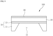
- FIG. 1 is a cross-sectional view showing a pellicle for extreme ultraviolet lithography using directly grown multilayer graphene according to the present disclosure.
- a pellicle 100 for extreme ultraviolet lithography includes a silicon nitride substrate 10, a core layer 20, and a capping layer 30.
- the silicon nitride substrate 10 has an opening 15 formed in a center portion.
- the core layer 20 and the capping layer 30 are formed on the silicon nitride substrate 10 so as to cover the opening 15.
- the pellicle 100 is a consumable component that protects a mask from contaminants in a lithography process for semiconductor or display manufacturing. That is, the pellicle 100 is a thin film overlying the mask and serves as a cover. Because the light transferred to the wafer is focused with the mask in a lithographic exposure, even if contaminants exist on the pellicle 100 that is separated by a certain distance, it is possible to minimize a problem of forming a defective pattern due to out of focus.
- the pellicle 100 may minimize defective patterns while protecting the mask from contaminants during the exposure process, thereby greatly increasing the yield of semiconductor or display manufacturing.
- the use of the pellicle 100 can increase the lifespan of the mask.
- the silicon nitride substrate 10 supports the core layer 20 and the capping layer 30 and makes it easy to handle and transport the pellicle 100 during and after the process of manufacturing the pellicle 100.
- the silicon nitride substrate 10 may be formed of a material available for an etching process.
- the silicon nitride substrate 10 includes a silicon substrate 11 and a support layer 13 made of a silicon nitride material and formed on the silicon substrate 11.
- the core layer 20 is formed on the support layer 13.
- the material of the support layer 13 may be represented by SiN x .
- the support layer 13 may be formed of Si 3 N 4 .
- the opening 15 in the central portion of the silicon nitride substrate 10 may be formed using a micro-machining technique such as micro-electro mechanical systems (MEMS). That is, the opening 15 is formed by removing the central portion of the silicon substrate 11 under the support layer 13 by means of the micro-machining technique. The opening 15 partially exposes the support layer 13 under the core layer 20.
- MEMS micro-electro mechanical systems
- the core layer 20 is a layer that determines the transmittance of extreme ultraviolet rays, and is formed of multilayer graphene.
- the core layer 20 has a transmittance of 90% or more for extreme ultraviolet rays, and effectively dissipates heat to prevent overheating.
- the core layer 20 may have a thickness greater than the sum of the thicknesses of the support layer 13 and the capping layer 30.
- the multilayer graphene forming the core layer 20 is formed by direct growth through interlayer exchange by heat exchange on the basis of few-layer graphene formed on the support layer 13.
- the direct growth method of multilayer graphene according to the present disclosure will be described in the manufacturing method of the pellicle 100.
- the capping layer 30 provides thermal stability, mechanical stability, and chemical durability to the core layer 20 while minimizing a decrease in the transmittance of the core layer 20 for extreme ultraviolet rays.
- the capping layer 30 is a protective layer for the core layer 20 and provides thermal stability by effectively dissipating heat generated in the core layer 20 to the outside.
- the capping layer 30 provides mechanical stability by supplementing the mechanical strength of the core layer 20.
- the capping layer 30 provides chemical durability by protecting the core layer 20 from hydrogen radicals and oxidation.
- the capping layer 30 may include SiN x , BN, ZrB x (2 ⁇ x ⁇ 16), ZrB x Si y (x ⁇ 2, y ⁇ 2), Si-BN, or Zr.
- the capping layer 30 may be formed by a chemical vapor deposition (CVD) process, but is formed by an atomic layer deposition (ALD) process or an ion beam sputtering deposition (IBSD) process, so that the best transmittance and minimized defects can be realized through free control of thickness, physical properties, and chemical composition.
- the capping layer 30 may be formed on the core layer 20 to have a thickness of 1 nm to 5 nm.
- the capping layer 30 is formed with a thickness of 3 nm to 4 nm on the core layer 20.
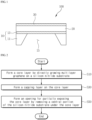
- FIG. 2 is a flowchart showing a method of manufacturing a pellicle for extreme ultraviolet lithography using a direct growth method of multilayer graphene according to the present disclosure.
- FIG. 3 is a detailed flowchart showing the step of forming the core layer of FIG. 2 .
- the method for manufacturing a pellicle according to the present disclosure includes a step S10 of forming a core layer by directly growing multilayer graphene on a silicon nitride substrate, a step S30 of forming a capping layer on the core layer, and a step S50 of forming an opening for partially exposing the core layer by removing a central portion of the silicon nitride substrate under the core layer.
- the step S10 of forming the core layer includes a step S11 of forming few-layer graphene on a support layer of the silicon nitride substrate, a step S13 of forming a metal catalyst layer on the few-layer graphene, a step S15 of forming an amorphous carbon layer on the metal catalyst layer, and a step S17 of directly growing multilayer graphene from the few-layer graphene by interlayer exchange between the metal catalyst layer and the amorphous carbon layer through heat treatment. Then, after the step S17 of directly growing the multilayer graphene, a step S19 of removing the metal catalyst layer on the multilayer graphene is performed.
- FIGS. 4 to 9 are views showing respective steps in the manufacturing method shown in FIG 2 .
- FIGS. 5 to 8 are enlarged views of part 'A' of FIG. 4 .
- the core layer 20 is formed on the silicon nitride substrate 10 through a direct growth of multilayer graphene 23.
- the silicon nitride substrate 10 is prepared.
- the silicon nitride substrate 10 is composed of the silicon substrate 11 and the support layer 13 formed on the silicon substrate 11.
- the support layer 13 is made of a silicon nitride material such as Si 3 N 4 .
- few-layer graphene 21, a metal catalyst layer 25, and an amorphous carbon layer 27 are sequentially stacked on the support layer 13 of the silicon nitride substrate 10 at the steps S11 to S15.
- the few-layer graphene 21 is formed on the support layer 13.
- the few-layer graphene 21 is graphene with five or less layers.
- the few-layer graphene 21 is a seed layer of the multilayer graphene, and is a diffusion barrier that prevents metal of the metal catalyst layer 25 from diffusing into the silicon nitride substrate 10.
- the few-layer graphene 21 may be formed on the support layer 13 by means of transferring technique. That is, after growing the few-layer graphene 21 on a nickel thin film or a copper thin film by the CVD process, the grown few-layer graphene 21 may be transferred onto the support layer 13.
- the metal catalyst layer 25 is formed on the few-layer graphene 21.
- the material of the metal catalyst layer 25 may include Ni, Co, Ru, or Pt.
- the metal catalyst layer 25 is formed to have a thickness of 10 nm to 100 nm by a sputtering process or an e-beam evaporation process.
- the amorphous carbon layer 27 is formed on the metal catalyst layer 25. That is, the amorphous carbon layer 27 is formed to have a thickness of 10 nm to 100 nm by the sputtering process.
- the multilayer graphene 23 is directly grown from the few-layer graphene (21 in FIG. 5 ) at the step S17 by interlayer exchange between the metal catalyst layer 25 and the amorphous carbon layer 27 through heat treatment.
- the multilayer graphene 23 is directly grown on the silicon nitride substrate 10 by means of the interlayer exchange principle. That is, when the metal catalyst layer 25 and the amorphous carbon layer 27 are sequentially formed on the few-layer graphene 21 and then subjected to heat treatment, carbon in the amorphous carbon layer 27 is moved to the few-layer graphene 21 by the interlayer exchange principle to directly grow the multilayer graphene 23.
- a driving force of the interlayer exchange is because the Gibbs free energy is lowered when the amorphous carbon becomes a crystalline state. Therefore, if the few-layer graphene 21 acting as a seed layer is placed under the metal catalyst layer 25, the interlayer exchanges can occur wholly and smoothly even if the heat treatment is performed at a temperature lower than a conventional heat treatment temperature for growing the multilayer graphene.
- the heat treatment according to the present disclosure may be performed at 500 to 1100°C for 10 minutes to 10 hours in a hydrogen gas and inert gas atmosphere.
- the inert gas may include at least one of nitrogen, argon, and helium.
- the manufacturing process of the multilayer graphene 23 can be simplified in manufacturing the pellicle.
- the few-layer graphene 21 functions as a diffusion barrier that prevents metal of the metal catalyst layer 25 from diffusing into the silicon nitride substrate 10 during the heat treatment process, the quality of the multilayer graphene 23 directly grown on the silicon nitride substrate 10 can be improved.
- the metal catalyst layer (25 in FIG. 6 ) on the multilayer graphene (23 in FIG. 6 ) is removed, so that the core layer 20 formed of multilayer graphene is obtained.
- the metal catalyst layer 25 on the multilayer graphene 23 may be removed through selective etching of the metal catalyst layer 25.
- the capping layer 30 is formed on the core layer 20 at the step S30.
- the capping layer 30 is formed with a thickness of 1 nm to 5 nm on the core layer 20 by the ALD or IBSD process.
- the capping layer 30 may include SiN x , BN, ZrB x (2 ⁇ x ⁇ 16), ZrB x Si y (x ⁇ 2, y ⁇ 2), Si-BN, or Zr.
- the opening 15 through which the core layer 20 is partially exposed is formed at the step S50 by removing the central portion of the silicon nitride substrate 10 under the core layer 20.
- the pellicle 100 according to the present disclosure is obtained.
- the central portion of the silicon substrate 11 under the support layer 13 is removed through a wet etching process.
- the opening 15 partially exposes the support layer 13 under the core layer 20.
- the pellicle 100 manufactured by the above-described manufacturing method of the present disclosure includes the multilayer graphene 23 as the core layer 20, so it can provide thermal stability, mechanical stability, and chemical durability while having a high extreme ultraviolet transmittance of 90% or more.
- the multilayer graphene 23 manufactured by the above-described manufacturing method of the present disclosure is employed as the core layer 20, and the support layer 13 and the capping layer 30 of several nanometers are formed on both sides of the core layer 20, it is possible to provide an extreme ultraviolet transmittance of 90% or more and a maximum reflectance of 0.0005%.
- the capping layer 30 in the ALD or IBSD process, it is possible to realize the best transmittance and minimized defects through free control of thickness, physical properties, and chemical composition.
- a pellicle according to an embodiment not encompassed by the wording of the claims was manufactured using the manufacturing method according to the present disclosure, and transmittance and reflectance were measured.
- the pellicle according to the embodiment has a structure in which a silicon nitride layer (support layer) of Si 3 N 4 , a core layer of multilayer graphene, and a capping layer of Si 3 N 4 are formed on a silicon substrate.
- the pellicle according to the embodiment is denoted by Si 3 N 4 _C_ Si 3 N 4 .
- FIG. 10 is a graph showing the extreme ultraviolet transmittance of a pellicle according to an embodiment.
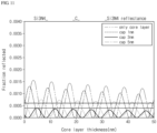
- FIG. 11 is a graph showing the extreme ultraviolet reflectance of a pellicle according to an embodiment.
- FIG. 12 is a graph showing the maximum extreme ultraviolet reflectance of a pellicle according to an embodiment.
- the transmittance and reflectance of the pellicle according to the embodiment were simulated in an extreme ultraviolet output environment of 350 W.
- the transmittance of the pellicle according to the embodiment decreases as the thickness of the capping layer increases.
- the thickness of the core layer is as follows.
- the capping layer has a thickness of 0 nm, that is, when there is only the core layer without the capping layer, the thickness of the core layer is 16.4 nm or less.
- the thickness of the core layer is 14 nm or less.
- the thickness of the core layer is 8.6 nm or less.
- the thickness of the core layer is 2.9 nm or less.
- the capping layer is formed to have a thickness of 3 nm to 4 nm so that the pellicle according to the embodiment has an extreme ultraviolet transmittance of 90% or more.
- the reflectance of the pellicle according to the embodiment is 0.0015% or less when the capping layer is formed to have a thickness of 1 to 5 nm and the core layer is formed to have a thickness of 50 nm or less.
- the thickness of the capping layer for controlling the maximum reflectance of the pellicle according to the embodiment to be 0.0005% or less is between 2 nm and 5 nm. In this case, the thickness of the core layer is irrelevant.
- the capping layer is formed to have a thickness of 3 nm to 4 nm.
- FIGS. 13 and 14 are graphs showing analysis results of Raman spectroscopy for each heat treatment temperature of multilayer graphene according to an embodiment not encompassed by the wording of the claims.
- FIG. 13 shows an analysis result of Raman spectroscopy for each heat treatment temperature of multilayer graphene as viewed from the metal catalyst layer.
- FIG. 14 shows an analysis result of Raman spectroscopy for each heat treatment temperature of multilayer graphene as viewed from the silicon nitride layer. Heat treatment was carried out at 700°C, 800°C, and 900°C. The thickness of the amorphous carbon layer is 30 nm.
- FIGS. 15 and 16 are graphs showing analysis results of Raman spectroscopy for each thickness of an amorphous carbon layer forming multilayer graphene according to an embodiment not encompassed by the wording of the claims.
- FIG. 15 shows an analysis result of Raman spectroscopy for each amorphous carbon layer thickness of multilayer graphene as viewed from the metal catalyst layer.
- FIG. 16 shows an analysis result of Raman spectroscopy for each amorphous carbon layer thickness of the multilayer graphene as viewed from the silicon nitride layer. Heat treatment was performed at 700°C. The thickness of the amorphous carbon layer was changed to 10 nm, 20 nm, and 30 nm.
Landscapes
- Chemical & Material Sciences (AREA)
- Organic Chemistry (AREA)
- Engineering & Computer Science (AREA)
- Materials Engineering (AREA)
- Physics & Mathematics (AREA)
- General Physics & Mathematics (AREA)
- Inorganic Chemistry (AREA)
- Nanotechnology (AREA)
- Chemical Kinetics & Catalysis (AREA)
- Health & Medical Sciences (AREA)
- Environmental & Geological Engineering (AREA)
- Epidemiology (AREA)
- Public Health (AREA)
- Preparing Plates And Mask In Photomechanical Process (AREA)
- Carbon And Carbon Compounds (AREA)
Claims (15)
- Verfahren für das direkte Wachstum von mehrschichtigem Graphen (23), das in einem Pellikel (100) für die EUV-Lithographie verwendet wird, wobei das Verfahren Folgendes umfasst:Bilden von Graphen (21) aus wenigen Schichten auf einem Siliciumnitridsubstrat (10);Bilden einer Metallkatalysatorschicht (25) auf dem Graphen (21) aus wenigen Schichten;Bilden einer Schicht (27) aus amorphem Kohlenstoff auf der Metallkatalysatorschicht (25) unddirektes Wachsenlassen von mehrschichtigem Graphen (23) aus dem Graphen (21) aus wenigen Schichten, das als Keimschicht verwendet wird, durchZwischenschichtaustausch zwischen derMetallkatalysatorschicht (25) und der Schicht (27) aus amorphem Kohlenstoff über Wärmebehandlung, wobei Kohlenstoff in der Schicht (27) aus amorphem Kohlenstoff durch die Metallkatalysatorschicht (25) wandert und zum Graphen (21) aus wenigen Schichten transportiert wird.
- Verfahren nach Anspruch 1, wobei das
Siliciumnitridsubstrat (10) für das Pellikel (100) für die EUV-Lithographie verwendet wird und ein Siliciumsubstrat (11) und eine Trägerschicht (13) aufweist, die aus einem Siliciumnitridmaterial gefertigt und auf dem Siliciumsubstrat (11) gebildet wird, und wobei das Graphen (21) aus wenigen Schichten auf der Trägerschicht (13) gebildet wird. - Verfahren nach Anspruch 2, wobei das Graphen (21) aus wenigen Schichten Graphen mit maximal fünf Schichten ist.
- Verfahren nach Anspruch 3, wobei das Graphen (21) aus wenigen Schichten auf der Trägerschicht (13) mit einem Übertragungsverfahren gebildet wird.
- Verfahren nach Anspruch 3, wobei das Graphen (21) aus wenigen Schichten eine Diffusionsbarriere ist, mit der verhindert werden soll, dass Metall aus der Metallkatalysatorschicht (25) in das Siliciumnitridsubstrat (10) diffundiert.
- Verfahren nach Anspruch 3, wobei ein Material der Metallkatalysatorschicht (25) Ni, Co, Ru oder Pt aufweist.
- Verfahren nach Anspruch 6, wobei die
Metallkatalysatorschicht (25) mit einem Sputterverfahren oder einem Elektronenstrahlverdampfungsverfahren so gebildet wird, dass sie eine Dicke von 10 nm bis 100 nm aufweist. - Verfahren nach Anspruch 3, wobei die Schicht (27) aus amorphem Kohlenstoff mit einem Sputterverfahren so gebildet wird, dass sie eine Dicke von 10 nm bis 100 nm aufweist.
- Verfahren nach Anspruch 1, wobei die Wärmebehandlung 10 Minuten bis 10 Stunden lang bei 500 bis 1100 °C in einer Wasserstoff- und Inertgasatmosphäre durchgeführt wird und das Inertgas Stickstoff, Argon und/oder Helium umfasst.
- Verfahren nach Anspruch 1, ferner umfassend:
nach dem direkten Wachsenlassen des mehrschichtigen Graphens (23) Entfernen der Metallkatalysatorschicht (25) auf dem mehrschichtigen Graphen (23). - Verfahren zum Herstellen eines Pellikels (100) für die EUV-Lithographie durch Einsatz von direktem Wachstum von mehrschichtigem Graphen (23), wobei das Verfahren Folgendes umfasst:Bilden einer Kernschicht (20) durch direktes Wachsenlassen von mehrschichtigem Graphen (23) auf einem Siliciumnitridsubstrat (10);Bilden einer Deckschicht (30) auf der Kernschicht(20); undBilden einer Öffnung (15) zum teilweisen Freilegen der Kernschicht (20) durch Entfernen eines mittigen Abschnitts des Siliciumnitridsubstrats (10) unter der Kernschicht (20),wobei das Bilden der Kernschicht (20) Folgendes umfasst:Bilden von Graphen (21) aus wenigen Schichten auf dem Siliciumnitridsubstrat (10);Bilden einer Metallkatalysatorschicht (25) auf dem Graphen (21) aus wenigen Schichten;Bilden einer Schicht (27) aus amorphem Kohlenstoff auf der Metallkatalysatorschicht (25);direktes Wachsenlassen von mehrschichtigem Graphen (23) aus dem Graphen (21) aus wenigen Schichten, das als Keimschicht verwendet wird, durchZwischenschichtaustausch zwischen derMetallkatalysatorschicht (25) und der Schicht (27) aus amorphem Kohlenstoff über Wärmebehandlung, wobei Kohlenstoff in der Schicht (27) aus amorphem Kohlenstoff durch die Metallkatalysatorschicht (25) wandert und zum Graphen (21) aus wenigen Schichten transportiert wird; undEntfernen der Metallkatalysatorschicht (25) auf dem mehrschichtigen Graphen (23).
- Verfahren nach Anspruch 11, wobei dasSiliciumnitridsubstrat (10) ein Siliciumsubstrat (11) und eine Trägerschicht (13) aufweist, die aus einem Siliciumnitridmaterial gefertigt und auf dem Siliciumsubstrat (11) gebildet wird,wobei das Graphen (21) aus wenigen Schichten auf der Trägerschicht (13) gebildet wird undwobei die Öffnung (15) durch Entfernen eines mittigen Abschnitts des Siliciumsubstrats (11) unter der Trägerschicht (13) gebildet wird.
- Verfahren nach Anspruch 12, wobei das Graphen (21) aus wenigen Schichten Graphen mit maximal fünf Schichten ist und eine Diffusionsbarriere ist, mit der verhindert werden soll, dass Metall aus der Metallkatalysatorschicht (25) in das Siliciumnitridsubstrat (10) diffundiert.
- Verfahren nach Anspruch 11, wobei ein Material der Deckschicht (30) SiNx, BN, ZrBx mit 2 ≤ x < 16, ZrBxSiy mit x ≥ 2, y ≥ 2, Si-BN oder Zr umfasst.
- Verfahren nach Anspruch 14, wobei die Deckschicht (30) mit einem Atomlagenabscheideverfahren oder einem Abscheideverfahren mittels Ionenstrahlsputtern so auf der Kernschicht (20) gebildet wird, dass sie eine Dicke von 1 nm bis 5 nm aufweist.
Applications Claiming Priority (1)
| Application Number | Priority Date | Filing Date | Title |
|---|---|---|---|
| KR1020200149813A KR102282184B1 (ko) | 2020-11-11 | 2020-11-11 | 다층 그래핀의 직성장 방법 및 그를 이용한 극자외선 노광용 펠리클의 제조 방법 |
Publications (2)
| Publication Number | Publication Date |
|---|---|
| EP4002007A1 EP4002007A1 (de) | 2022-05-25 |
| EP4002007B1 true EP4002007B1 (de) | 2023-10-18 |
Family
ID=77126411
Family Applications (1)
| Application Number | Title | Priority Date | Filing Date |
|---|---|---|---|
| EP21207713.5A Active EP4002007B1 (de) | 2020-11-11 | 2021-11-11 | Verfahren zur direkten züchtung von mehrschichtigen graphenen und verfahren zur herstellung eines pellikels für extreme ultraviolette lithographie damit |
Country Status (4)
| Country | Link |
|---|---|
| US (1) | US12248243B2 (de) |
| EP (1) | EP4002007B1 (de) |
| JP (1) | JP7320039B2 (de) |
| KR (1) | KR102282184B1 (de) |
Families Citing this family (6)
| Publication number | Priority date | Publication date | Assignee | Title |
|---|---|---|---|---|
| KR102558500B1 (ko) | 2021-04-08 | 2023-07-21 | 한국전자기술연구원 | 다층 그래핀의 저온 직성장 방법, 그를 이용한 극자외선 노광용 펠리클 및 그의 제조 방법 |
| KR102705080B1 (ko) * | 2021-04-14 | 2024-09-11 | 한국전자기술연구원 | 극자외선 노광용 펠리클 |
| KR102442672B1 (ko) * | 2022-03-29 | 2022-09-13 | 주식회사 그래핀랩 | 탄소계 박막 쉐도우 마스크 및 그 제조방법 |
| KR102442676B1 (ko) | 2022-04-15 | 2022-09-14 | 주식회사 그래핀랩 | 오존가스를 이용한 펠리클 소재용 그래핀박막의 제조방법 |
| KR20240049899A (ko) * | 2022-10-11 | 2024-04-18 | 주식회사 그래핀랩 | 펠리클 제조 방법 |
| KR20230171906A (ko) | 2023-04-03 | 2023-12-21 | 포항공과대학교 산학협력단 | Euv 리소그래피용 펠리클 구조체, 및 그 제조 방법, 그리고 제조 장치, 그리고 이를 포함하는 euv 리소그래피 장치 |
Citations (2)
| Publication number | Priority date | Publication date | Assignee | Title |
|---|---|---|---|---|
| US20120267041A1 (en) * | 2011-04-22 | 2012-10-25 | Samsung Electronics Co., Ltd. | Method of forming multi-layer graphene |
| JP2018035010A (ja) * | 2016-08-29 | 2018-03-08 | 国立大学法人 筑波大学 | 多層グラフェンの製造方法及び多層グラフェン積層体 |
Family Cites Families (19)
| Publication number | Priority date | Publication date | Assignee | Title |
|---|---|---|---|---|
| JP2006170916A (ja) | 2004-12-17 | 2006-06-29 | Nikon Corp | 光学素子及びこれを用いた投影露光装置 |
| US8927057B2 (en) | 2010-02-22 | 2015-01-06 | International Business Machines Corporation | Graphene formation utilizing solid phase carbon sources |
| KR101878733B1 (ko) | 2011-05-04 | 2018-07-16 | 삼성전자주식회사 | 그래핀 직성장 방법 |
| WO2016001351A1 (en) | 2014-07-04 | 2016-01-07 | Asml Netherlands B.V. | Membranes for use within a lithographic apparatus and a lithographic apparatus comprising such a membrane |
| DE102014115708A1 (de) | 2014-10-29 | 2016-05-04 | Aixtron Se | Verfahren zum Trennen einer Kohlenstoffstruktur von einer Keimstruktur |
| CN104477903A (zh) | 2014-12-22 | 2015-04-01 | 上海集成电路研发中心有限公司 | 一种石墨烯薄膜的制备方法 |
| NL2017606A (en) * | 2015-10-22 | 2017-05-10 | Asml Netherlands Bv | A method of manufacturing a pellicle for a lithographic apparatus, a pellicle for a lithographic apparatus, a lithographic apparatus, a device manufacturing method, an apparatus for processing a pellicle, and a method for processing a pellicle |
| US11320731B2 (en) | 2015-12-14 | 2022-05-03 | Asml Netherlands B.V. | Membrane for EUV lithography |
| KR101762059B1 (ko) | 2016-01-13 | 2017-07-31 | 한양대학교 산학협력단 | Euv 펠리클 구조체, 및 그 제조 방법 |
| CA3021916A1 (en) | 2016-04-25 | 2017-11-02 | Asml Netherlands B.V. | A membrane for euv lithography |
| KR101981950B1 (ko) * | 2017-11-10 | 2019-05-24 | 주식회사 에스앤에스텍 | 극자외선 리소그래피용 펠리클 |
| JP7368363B2 (ja) | 2018-03-09 | 2023-10-24 | エーエスエムエル ネザーランズ ビー.ブイ. | グラフェンペリクルリソグラフィ装置 |
| JP2020098227A (ja) * | 2018-12-17 | 2020-06-25 | 信越化学工業株式会社 | フォトリソグラフィ用ペリクル膜及びこれを備えたペリクル |
| KR20200126216A (ko) | 2019-04-29 | 2020-11-06 | 주식회사 에스앤에스텍 | 극자외선 리소그래피용 펠리클 및 이의 제조방법 |
| KR102247692B1 (ko) * | 2020-08-19 | 2021-04-30 | 성균관대학교산학협력단 | 펠리클 구조체 및 이의 제조방법 |
| KR20220062799A (ko) | 2020-11-09 | 2022-05-17 | 한국전자기술연구원 | 극자외선 노광용 펠리클 |
| KR102317053B1 (ko) * | 2020-12-02 | 2021-10-26 | 한국전자기술연구원 | 그래핀 결함 치유층을 구비하는 극자외선 노광용 펠리클 및 그의 제조 방법 |
| KR102558500B1 (ko) | 2021-04-08 | 2023-07-21 | 한국전자기술연구원 | 다층 그래핀의 저온 직성장 방법, 그를 이용한 극자외선 노광용 펠리클 및 그의 제조 방법 |
| KR102694335B1 (ko) | 2021-10-25 | 2024-08-12 | 한국전자기술연구원 | 탄화이트륨 기반의 극자외선 노광용 펠리클 |
-
2020
- 2020-11-11 KR KR1020200149813A patent/KR102282184B1/ko active Active
-
2021
- 2021-11-10 US US17/454,377 patent/US12248243B2/en active Active
- 2021-11-11 JP JP2021183857A patent/JP7320039B2/ja active Active
- 2021-11-11 EP EP21207713.5A patent/EP4002007B1/de active Active
Patent Citations (2)
| Publication number | Priority date | Publication date | Assignee | Title |
|---|---|---|---|---|
| US20120267041A1 (en) * | 2011-04-22 | 2012-10-25 | Samsung Electronics Co., Ltd. | Method of forming multi-layer graphene |
| JP2018035010A (ja) * | 2016-08-29 | 2018-03-08 | 国立大学法人 筑波大学 | 多層グラフェンの製造方法及び多層グラフェン積層体 |
Also Published As
| Publication number | Publication date |
|---|---|
| JP2022077526A (ja) | 2022-05-23 |
| US20220146928A1 (en) | 2022-05-12 |
| KR102282184B1 (ko) | 2021-07-28 |
| JP7320039B2 (ja) | 2023-08-02 |
| US12248243B2 (en) | 2025-03-11 |
| EP4002007A1 (de) | 2022-05-25 |
Similar Documents
| Publication | Publication Date | Title |
|---|---|---|
| EP4002007B1 (de) | Verfahren zur direkten züchtung von mehrschichtigen graphenen und verfahren zur herstellung eines pellikels für extreme ultraviolette lithographie damit | |
| US11789359B2 (en) | Method for manufacturing pellicle for extreme ultraviolet lithography having graphene defect healing layer | |
| CN111836681B (zh) | 石墨烯表膜光刻设备 | |
| US12321092B2 (en) | Pellicle for extreme ultraviolet lithography containing amorphous carbon and method for manufacturing the same | |
| US11927881B2 (en) | Pellicle for extreme ultraviolet lithography based on yttrium carbide | |
| US12287568B2 (en) | Low-temperature direct growth method of multilayer graphene, pellicle for extreme ultraviolet lithography using the same, and method for manufacturing the pellicle | |
| KR102482649B1 (ko) | 극자외선 리소그라피용 펠리클의 제조방법 | |
| US20220260932A1 (en) | Optical assembly with coating and methods of use | |
| CN115903372A (zh) | 具有涂层的光学组件和使用方法 | |
| US20220326603A1 (en) | Pellicle for extreme ultraviolet lithography containing molybdenum carbide | |
| CN114690544A (zh) | 光罩表层膜及其形成方法 | |
| KR20240109601A (ko) | 이트륨계 기반의 극자외선 노광용 펠리클 | |
| WO2024155654A1 (en) | Extreme ultraviolet pellicles and method of manufacturing | |
| CN117170179A (zh) | 用于euv光刻掩模的薄膜及其制造方法 | |
| TWI861999B (zh) | 用於極紫外光微影光罩的光罩護膜及其製造方法 | |
| KR20240142787A (ko) | 다공성 Mo2C 박막의 제조 방법 및 그를 이용한 극자외선 리소그래피용 펠리클 | |
| KR20220139670A (ko) | 가압 열처리를 통한 다층 그래핀의 직성장 방법 및 그를 이용한 극자외선 노광용 펠리클의 제조 방법 | |
| KR20220141374A (ko) | 이트륨화합물을 함유하는 극자외선 노광용 펠리클 |
Legal Events
| Date | Code | Title | Description |
|---|---|---|---|
| PUAI | Public reference made under article 153(3) epc to a published international application that has entered the european phase |
Free format text: ORIGINAL CODE: 0009012 |
|
| STAA | Information on the status of an ep patent application or granted ep patent |
Free format text: STATUS: REQUEST FOR EXAMINATION WAS MADE |
|
| 17P | Request for examination filed |
Effective date: 20211111 |
|
| AK | Designated contracting states |
Kind code of ref document: A1 Designated state(s): AL AT BE BG CH CY CZ DE DK EE ES FI FR GB GR HR HU IE IS IT LI LT LU LV MC MK MT NL NO PL PT RO RS SE SI SK SM TR |
|
| RBV | Designated contracting states (corrected) |
Designated state(s): AL AT BE BG CH CY CZ DE DK EE ES FI FR GB GR HR HU IE IS IT LI LT LU LV MC MK MT NL NO PL PT RO RS SE SI SK SM TR |
|
| GRAP | Despatch of communication of intention to grant a patent |
Free format text: ORIGINAL CODE: EPIDOSNIGR1 |
|
| STAA | Information on the status of an ep patent application or granted ep patent |
Free format text: STATUS: GRANT OF PATENT IS INTENDED |
|
| RIC1 | Information provided on ipc code assigned before grant |
Ipc: C01B 32/184 20170101ALI20230418BHEP Ipc: B82Y 40/00 20110101ALI20230418BHEP Ipc: B82Y 30/00 20110101ALI20230418BHEP Ipc: B01J 23/28 20060101ALI20230418BHEP Ipc: G03F 1/62 20120101AFI20230418BHEP |
|
| INTG | Intention to grant announced |
Effective date: 20230515 |
|
| GRAS | Grant fee paid |
Free format text: ORIGINAL CODE: EPIDOSNIGR3 |
|
| GRAA | (expected) grant |
Free format text: ORIGINAL CODE: 0009210 |
|
| STAA | Information on the status of an ep patent application or granted ep patent |
Free format text: STATUS: THE PATENT HAS BEEN GRANTED |
|
| AK | Designated contracting states |
Kind code of ref document: B1 Designated state(s): AL AT BE BG CH CY CZ DE DK EE ES FI FR GB GR HR HU IE IS IT LI LT LU LV MC MK MT NL NO PL PT RO RS SE SI SK SM TR |
|
| REG | Reference to a national code |
Ref country code: GB Ref legal event code: FG4D |
|
| REG | Reference to a national code |
Ref country code: CH Ref legal event code: EP |
|
| REG | Reference to a national code |
Ref country code: IE Ref legal event code: FG4D |
|
| REG | Reference to a national code |
Ref country code: DE Ref legal event code: R096 Ref document number: 602021005992 Country of ref document: DE |
|
| REG | Reference to a national code |
Ref country code: NL Ref legal event code: FP |
|
| REG | Reference to a national code |
Ref country code: LT Ref legal event code: MG9D |
|
| REG | Reference to a national code |
Ref country code: AT Ref legal event code: MK05 Ref document number: 1622973 Country of ref document: AT Kind code of ref document: T Effective date: 20231018 |
|
| PG25 | Lapsed in a contracting state [announced via postgrant information from national office to epo] |
Ref country code: GR Free format text: LAPSE BECAUSE OF FAILURE TO SUBMIT A TRANSLATION OF THE DESCRIPTION OR TO PAY THE FEE WITHIN THE PRESCRIBED TIME-LIMIT Effective date: 20240119 |
|
| PG25 | Lapsed in a contracting state [announced via postgrant information from national office to epo] |
Ref country code: IS Free format text: LAPSE BECAUSE OF FAILURE TO SUBMIT A TRANSLATION OF THE DESCRIPTION OR TO PAY THE FEE WITHIN THE PRESCRIBED TIME-LIMIT Effective date: 20240218 |
|
| PG25 | Lapsed in a contracting state [announced via postgrant information from national office to epo] |
Ref country code: LT Free format text: LAPSE BECAUSE OF FAILURE TO SUBMIT A TRANSLATION OF THE DESCRIPTION OR TO PAY THE FEE WITHIN THE PRESCRIBED TIME-LIMIT Effective date: 20231018 |
|
| PG25 | Lapsed in a contracting state [announced via postgrant information from national office to epo] |
Ref country code: AT Free format text: LAPSE BECAUSE OF FAILURE TO SUBMIT A TRANSLATION OF THE DESCRIPTION OR TO PAY THE FEE WITHIN THE PRESCRIBED TIME-LIMIT Effective date: 20231018 |
|
| PG25 | Lapsed in a contracting state [announced via postgrant information from national office to epo] |
Ref country code: ES Free format text: LAPSE BECAUSE OF FAILURE TO SUBMIT A TRANSLATION OF THE DESCRIPTION OR TO PAY THE FEE WITHIN THE PRESCRIBED TIME-LIMIT Effective date: 20231018 |
|
| PG25 | Lapsed in a contracting state [announced via postgrant information from national office to epo] |
Ref country code: LT Free format text: LAPSE BECAUSE OF FAILURE TO SUBMIT A TRANSLATION OF THE DESCRIPTION OR TO PAY THE FEE WITHIN THE PRESCRIBED TIME-LIMIT Effective date: 20231018 Ref country code: IS Free format text: LAPSE BECAUSE OF FAILURE TO SUBMIT A TRANSLATION OF THE DESCRIPTION OR TO PAY THE FEE WITHIN THE PRESCRIBED TIME-LIMIT Effective date: 20240218 Ref country code: GR Free format text: LAPSE BECAUSE OF FAILURE TO SUBMIT A TRANSLATION OF THE DESCRIPTION OR TO PAY THE FEE WITHIN THE PRESCRIBED TIME-LIMIT Effective date: 20240119 Ref country code: ES Free format text: LAPSE BECAUSE OF FAILURE TO SUBMIT A TRANSLATION OF THE DESCRIPTION OR TO PAY THE FEE WITHIN THE PRESCRIBED TIME-LIMIT Effective date: 20231018 Ref country code: BG Free format text: LAPSE BECAUSE OF FAILURE TO SUBMIT A TRANSLATION OF THE DESCRIPTION OR TO PAY THE FEE WITHIN THE PRESCRIBED TIME-LIMIT Effective date: 20240118 Ref country code: AT Free format text: LAPSE BECAUSE OF FAILURE TO SUBMIT A TRANSLATION OF THE DESCRIPTION OR TO PAY THE FEE WITHIN THE PRESCRIBED TIME-LIMIT Effective date: 20231018 Ref country code: PT Free format text: LAPSE BECAUSE OF FAILURE TO SUBMIT A TRANSLATION OF THE DESCRIPTION OR TO PAY THE FEE WITHIN THE PRESCRIBED TIME-LIMIT Effective date: 20240219 |
|
| PG25 | Lapsed in a contracting state [announced via postgrant information from national office to epo] |
Ref country code: SE Free format text: LAPSE BECAUSE OF FAILURE TO SUBMIT A TRANSLATION OF THE DESCRIPTION OR TO PAY THE FEE WITHIN THE PRESCRIBED TIME-LIMIT Effective date: 20231018 Ref country code: RS Free format text: LAPSE BECAUSE OF FAILURE TO SUBMIT A TRANSLATION OF THE DESCRIPTION OR TO PAY THE FEE WITHIN THE PRESCRIBED TIME-LIMIT Effective date: 20231018 Ref country code: PL Free format text: LAPSE BECAUSE OF FAILURE TO SUBMIT A TRANSLATION OF THE DESCRIPTION OR TO PAY THE FEE WITHIN THE PRESCRIBED TIME-LIMIT Effective date: 20231018 Ref country code: NO Free format text: LAPSE BECAUSE OF FAILURE TO SUBMIT A TRANSLATION OF THE DESCRIPTION OR TO PAY THE FEE WITHIN THE PRESCRIBED TIME-LIMIT Effective date: 20240118 Ref country code: LV Free format text: LAPSE BECAUSE OF FAILURE TO SUBMIT A TRANSLATION OF THE DESCRIPTION OR TO PAY THE FEE WITHIN THE PRESCRIBED TIME-LIMIT Effective date: 20231018 Ref country code: HR Free format text: LAPSE BECAUSE OF FAILURE TO SUBMIT A TRANSLATION OF THE DESCRIPTION OR TO PAY THE FEE WITHIN THE PRESCRIBED TIME-LIMIT Effective date: 20231018 |
|
| REG | Reference to a national code |
Ref country code: DE Ref legal event code: R119 Ref document number: 602021005992 Country of ref document: DE |
|
| PG25 | Lapsed in a contracting state [announced via postgrant information from national office to epo] |
Ref country code: DK Free format text: LAPSE BECAUSE OF FAILURE TO SUBMIT A TRANSLATION OF THE DESCRIPTION OR TO PAY THE FEE WITHIN THE PRESCRIBED TIME-LIMIT Effective date: 20231018 |
|
| PG25 | Lapsed in a contracting state [announced via postgrant information from national office to epo] |
Ref country code: LU Free format text: LAPSE BECAUSE OF NON-PAYMENT OF DUE FEES Effective date: 20231111 |
|
| PG25 | Lapsed in a contracting state [announced via postgrant information from national office to epo] |
Ref country code: CZ Free format text: LAPSE BECAUSE OF FAILURE TO SUBMIT A TRANSLATION OF THE DESCRIPTION OR TO PAY THE FEE WITHIN THE PRESCRIBED TIME-LIMIT Effective date: 20231018 |
|
| PG25 | Lapsed in a contracting state [announced via postgrant information from national office to epo] |
Ref country code: SK Free format text: LAPSE BECAUSE OF FAILURE TO SUBMIT A TRANSLATION OF THE DESCRIPTION OR TO PAY THE FEE WITHIN THE PRESCRIBED TIME-LIMIT Effective date: 20231018 |
|
| PG25 | Lapsed in a contracting state [announced via postgrant information from national office to epo] |
Ref country code: SM Free format text: LAPSE BECAUSE OF FAILURE TO SUBMIT A TRANSLATION OF THE DESCRIPTION OR TO PAY THE FEE WITHIN THE PRESCRIBED TIME-LIMIT Effective date: 20231018 Ref country code: SK Free format text: LAPSE BECAUSE OF FAILURE TO SUBMIT A TRANSLATION OF THE DESCRIPTION OR TO PAY THE FEE WITHIN THE PRESCRIBED TIME-LIMIT Effective date: 20231018 Ref country code: RO Free format text: LAPSE BECAUSE OF FAILURE TO SUBMIT A TRANSLATION OF THE DESCRIPTION OR TO PAY THE FEE WITHIN THE PRESCRIBED TIME-LIMIT Effective date: 20231018 Ref country code: LU Free format text: LAPSE BECAUSE OF NON-PAYMENT OF DUE FEES Effective date: 20231111 Ref country code: IT Free format text: LAPSE BECAUSE OF FAILURE TO SUBMIT A TRANSLATION OF THE DESCRIPTION OR TO PAY THE FEE WITHIN THE PRESCRIBED TIME-LIMIT Effective date: 20231018 Ref country code: EE Free format text: LAPSE BECAUSE OF FAILURE TO SUBMIT A TRANSLATION OF THE DESCRIPTION OR TO PAY THE FEE WITHIN THE PRESCRIBED TIME-LIMIT Effective date: 20231018 Ref country code: DK Free format text: LAPSE BECAUSE OF FAILURE TO SUBMIT A TRANSLATION OF THE DESCRIPTION OR TO PAY THE FEE WITHIN THE PRESCRIBED TIME-LIMIT Effective date: 20231018 Ref country code: CZ Free format text: LAPSE BECAUSE OF FAILURE TO SUBMIT A TRANSLATION OF THE DESCRIPTION OR TO PAY THE FEE WITHIN THE PRESCRIBED TIME-LIMIT Effective date: 20231018 |
|
| REG | Reference to a national code |
Ref country code: BE Ref legal event code: MM Effective date: 20231130 |
|
| PLBE | No opposition filed within time limit |
Free format text: ORIGINAL CODE: 0009261 |
|
| STAA | Information on the status of an ep patent application or granted ep patent |
Free format text: STATUS: NO OPPOSITION FILED WITHIN TIME LIMIT |
|
| PG25 | Lapsed in a contracting state [announced via postgrant information from national office to epo] |
Ref country code: MC Free format text: LAPSE BECAUSE OF FAILURE TO SUBMIT A TRANSLATION OF THE DESCRIPTION OR TO PAY THE FEE WITHIN THE PRESCRIBED TIME-LIMIT Effective date: 20231018 |
|
| PG25 | Lapsed in a contracting state [announced via postgrant information from national office to epo] |
Ref country code: MC Free format text: LAPSE BECAUSE OF FAILURE TO SUBMIT A TRANSLATION OF THE DESCRIPTION OR TO PAY THE FEE WITHIN THE PRESCRIBED TIME-LIMIT Effective date: 20231018 |
|
| REG | Reference to a national code |
Ref country code: IE Ref legal event code: MM4A |
|
| 26N | No opposition filed |
Effective date: 20240719 |
|
| PG25 | Lapsed in a contracting state [announced via postgrant information from national office to epo] |
Ref country code: DE Free format text: LAPSE BECAUSE OF NON-PAYMENT OF DUE FEES Effective date: 20240601 Ref country code: IE Free format text: LAPSE BECAUSE OF NON-PAYMENT OF DUE FEES Effective date: 20231111 |
|
| PG25 | Lapsed in a contracting state [announced via postgrant information from national office to epo] |
Ref country code: BE Free format text: LAPSE BECAUSE OF NON-PAYMENT OF DUE FEES Effective date: 20231130 |
|
| PG25 | Lapsed in a contracting state [announced via postgrant information from national office to epo] |
Ref country code: FR Free format text: LAPSE BECAUSE OF NON-PAYMENT OF DUE FEES Effective date: 20231218 |
|
| PG25 | Lapsed in a contracting state [announced via postgrant information from national office to epo] |
Ref country code: SI Free format text: LAPSE BECAUSE OF FAILURE TO SUBMIT A TRANSLATION OF THE DESCRIPTION OR TO PAY THE FEE WITHIN THE PRESCRIBED TIME-LIMIT Effective date: 20231018 |
|
| PG25 | Lapsed in a contracting state [announced via postgrant information from national office to epo] |
Ref country code: SI Free format text: LAPSE BECAUSE OF FAILURE TO SUBMIT A TRANSLATION OF THE DESCRIPTION OR TO PAY THE FEE WITHIN THE PRESCRIBED TIME-LIMIT Effective date: 20231018 Ref country code: IE Free format text: LAPSE BECAUSE OF NON-PAYMENT OF DUE FEES Effective date: 20231111 Ref country code: FR Free format text: LAPSE BECAUSE OF NON-PAYMENT OF DUE FEES Effective date: 20231218 Ref country code: DE Free format text: LAPSE BECAUSE OF NON-PAYMENT OF DUE FEES Effective date: 20240601 Ref country code: BE Free format text: LAPSE BECAUSE OF NON-PAYMENT OF DUE FEES Effective date: 20231130 |
|
| REG | Reference to a national code |
Ref country code: CH Ref legal event code: PL |
|
| PG25 | Lapsed in a contracting state [announced via postgrant information from national office to epo] |
Ref country code: FI Free format text: LAPSE BECAUSE OF FAILURE TO SUBMIT A TRANSLATION OF THE DESCRIPTION OR TO PAY THE FEE WITHIN THE PRESCRIBED TIME-LIMIT Effective date: 20231019 |
|
| REG | Reference to a national code |
Ref country code: CH Ref legal event code: PL |
|
| PG25 | Lapsed in a contracting state [announced via postgrant information from national office to epo] |
Ref country code: CH Free format text: LAPSE BECAUSE OF NON-PAYMENT OF DUE FEES Effective date: 20241130 |
|
| PG25 | Lapsed in a contracting state [announced via postgrant information from national office to epo] |
Ref country code: CY Free format text: LAPSE BECAUSE OF FAILURE TO SUBMIT A TRANSLATION OF THE DESCRIPTION OR TO PAY THE FEE WITHIN THE PRESCRIBED TIME-LIMIT; INVALID AB INITIO Effective date: 20211111 |
|
| PGFP | Annual fee paid to national office [announced via postgrant information from national office to epo] |
Ref country code: NL Payment date: 20250922 Year of fee payment: 5 |
|
| PG25 | Lapsed in a contracting state [announced via postgrant information from national office to epo] |
Ref country code: TR Free format text: LAPSE BECAUSE OF FAILURE TO SUBMIT A TRANSLATION OF THE DESCRIPTION OR TO PAY THE FEE WITHIN THE PRESCRIBED TIME-LIMIT Effective date: 20231018 |
|
| PG25 | Lapsed in a contracting state [announced via postgrant information from national office to epo] |
Ref country code: HU Free format text: LAPSE BECAUSE OF FAILURE TO SUBMIT A TRANSLATION OF THE DESCRIPTION OR TO PAY THE FEE WITHIN THE PRESCRIBED TIME-LIMIT; INVALID AB INITIO Effective date: 20211111 |