EP4001908A1 - Electrochemical sensor unit, electrode for electrochemical sensor, and method for manufacturing electrode for electrochemical sensor - Google Patents
Electrochemical sensor unit, electrode for electrochemical sensor, and method for manufacturing electrode for electrochemical sensor Download PDFInfo
- Publication number
- EP4001908A1 EP4001908A1 EP20843662.6A EP20843662A EP4001908A1 EP 4001908 A1 EP4001908 A1 EP 4001908A1 EP 20843662 A EP20843662 A EP 20843662A EP 4001908 A1 EP4001908 A1 EP 4001908A1
- Authority
- EP
- European Patent Office
- Prior art keywords
- diamond film
- electrode
- support
- electrochemical sensor
- diamond
- Prior art date
- Legal status (The legal status is an assumption and is not a legal conclusion. Google has not performed a legal analysis and makes no representation as to the accuracy of the status listed.)
- Withdrawn
Links
Images
Classifications
-
- G—PHYSICS
- G01—MEASURING; TESTING
- G01N—INVESTIGATING OR ANALYSING MATERIALS BY DETERMINING THEIR CHEMICAL OR PHYSICAL PROPERTIES
- G01N27/00—Investigating or analysing materials by the use of electric, electrochemical, or magnetic means
- G01N27/26—Investigating or analysing materials by the use of electric, electrochemical, or magnetic means by investigating electrochemical variables; by using electrolysis or electrophoresis
- G01N27/28—Electrolytic cell components
- G01N27/30—Electrodes, e.g. test electrodes; Half-cells
- G01N27/307—Disposable laminated or multilayered electrodes
-
- G—PHYSICS
- G01—MEASURING; TESTING
- G01N—INVESTIGATING OR ANALYSING MATERIALS BY DETERMINING THEIR CHEMICAL OR PHYSICAL PROPERTIES
- G01N27/00—Investigating or analysing materials by the use of electric, electrochemical, or magnetic means
- G01N27/26—Investigating or analysing materials by the use of electric, electrochemical, or magnetic means by investigating electrochemical variables; by using electrolysis or electrophoresis
- G01N27/28—Electrolytic cell components
- G01N27/30—Electrodes, e.g. test electrodes; Half-cells
- G01N27/308—Electrodes, e.g. test electrodes; Half-cells at least partially made of carbon
-
- C—CHEMISTRY; METALLURGY
- C23—COATING METALLIC MATERIAL; COATING MATERIAL WITH METALLIC MATERIAL; CHEMICAL SURFACE TREATMENT; DIFFUSION TREATMENT OF METALLIC MATERIAL; COATING BY VACUUM EVAPORATION, BY SPUTTERING, BY ION IMPLANTATION OR BY CHEMICAL VAPOUR DEPOSITION, IN GENERAL; INHIBITING CORROSION OF METALLIC MATERIAL OR INCRUSTATION IN GENERAL
- C23C—COATING METALLIC MATERIAL; COATING MATERIAL WITH METALLIC MATERIAL; SURFACE TREATMENT OF METALLIC MATERIAL BY DIFFUSION INTO THE SURFACE, BY CHEMICAL CONVERSION OR SUBSTITUTION; COATING BY VACUUM EVAPORATION, BY SPUTTERING, BY ION IMPLANTATION OR BY CHEMICAL VAPOUR DEPOSITION, IN GENERAL
- C23C16/00—Chemical coating by decomposition of gaseous compounds, without leaving reaction products of surface material in the coating, i.e. chemical vapour deposition [CVD] processes
- C23C16/22—Chemical coating by decomposition of gaseous compounds, without leaving reaction products of surface material in the coating, i.e. chemical vapour deposition [CVD] processes characterised by the deposition of inorganic material, other than metallic material
- C23C16/26—Deposition of carbon only
- C23C16/27—Diamond only
- C23C16/271—Diamond only using hot filaments
-
- G—PHYSICS
- G01—MEASURING; TESTING
- G01N—INVESTIGATING OR ANALYSING MATERIALS BY DETERMINING THEIR CHEMICAL OR PHYSICAL PROPERTIES
- G01N27/00—Investigating or analysing materials by the use of electric, electrochemical, or magnetic means
- G01N27/26—Investigating or analysing materials by the use of electric, electrochemical, or magnetic means by investigating electrochemical variables; by using electrolysis or electrophoresis
- G01N27/403—Cells and electrode assemblies
-
- G—PHYSICS
- G01—MEASURING; TESTING
- G01N—INVESTIGATING OR ANALYSING MATERIALS BY DETERMINING THEIR CHEMICAL OR PHYSICAL PROPERTIES
- G01N27/00—Investigating or analysing materials by the use of electric, electrochemical, or magnetic means
- G01N27/26—Investigating or analysing materials by the use of electric, electrochemical, or magnetic means by investigating electrochemical variables; by using electrolysis or electrophoresis
- G01N27/416—Systems
- G01N27/48—Systems using polarography, i.e. measuring changes in current under a slowly-varying voltage
Definitions
- the present disclosure relates to an electrochemical sensor unit, an electrode for electrochemical sensor, and a method of manufacturing an electrode for electrochemical sensor.
- an electrode including a diamond film as a working electrode for an electrochemical sensor unit. Since conductive diamond has a wide potential window and a small background current, it enables electrochemical detection of various substances with high sensitivity. Therefore, conductive diamond is attracting attention as a material for the electrode for electrochemical sensor.
- An object of the present disclosure is to further improve a sensor performance of an electrochemical sensor unit including an electrode for electrochemical sensor, the electrode including a diamond film.
- an electrochemical sensor unit and a related technique thereof including:
- an electrochemical sensor unit including an electrode for electrochemical sensor, the electrode including a diamond film.
- an electrochemical sensor unit 100 (hereafter also referred to as "sensor 100") according to the present embodiment includes: an electrode group 10 constituted by a working electrode 11, a counter electrode 12, and a reference electrode 13; a support member 20 which supports the electrode group 10; first to third wirings 31 to 33 connected to the working electrode 11, the counter electrode 12, and the reference electrode 13, respectively; a water absorption member 40 arranged so as to cover the electrode group 10; and a waterproof member 50 arranged so as to cover (a part of) the first to third wirings 31 to 33.
- the sensor 100 is configured to be disposable, for example.
- the working electrode 11 includes a diamond film which generates on a surface thereof a redox reaction (electrochemical reaction) of a predetermined component (e.g., uric acid) in urine when applying a predetermined voltage between the working electrode 11 and the counter electrode 12, both being in contact with a liquid test sample (e.g., urine), for example, using a measurement mechanism including a voltage applicator mentioned later.
- a redox reaction electrochemical reaction
- a predetermined component e.g., uric acid
- a liquid test sample e.g., urine
- the counter electrode 12 is an electrode for flowing a current generated by the above-mentioned redox reaction to the working electrode 11.
- an electrode formed of metal such as platinum (Pt), gold (Au), copper (Cu), palladium (Pd), nickel (Ni), or silver (Ag), a carbon electrode, or the like can be used.
- the reference electrode 13 is an electrode used as a basis for determining a potential of the working electrode 11.
- a silver/silver chloride (Ag/AgCl) electrode can be used.
- a standard hydrogen electrode, a reversible hydrogen electrode, a palladium-hydrogen electrode, a saturated calomel electrode, or the like can also be used.
- an electrode formed of metal such as Pt, Au, Cu, Pd, Ni, or Ag, a carbon electrode, or the like can be used.
- the working electrode 11, the counter electrode 12, and the reference electrode 13 are collectively referred to as the electrode group 10 in some cases.
- the sensor 100 includes the support member 20 which supports the electrode group 10.
- the electrode group 10 is arranged on the same surface of the support member 20.
- the support member 20 is configured as a sheet-like (plate-like) base material, and has a size and shape (e.g., a rectangular (strip-like) planar shape) that is easy-to-handle (e.g., easy for a subject to grasp).
- the support member 20 may include a longitudinal part (main part) and a convex part (a part connected to a measurement mechanism mentioned later).
- the support member 20 has such a physical (mechanical) strength that it can be used as the sensor 100.
- the support member 20 has such a strength that it does not bend nor break even when a test sample is attached thereto.
- the support member 20 can be formed of insulating materials such as insulating composite resin, ceramic, glass, plastic, flammable materials, biodegradable materials, non-woven fabric, or paper.
- the support member 20 is preferably a flexible base material.
- a base material formed of glass epoxy resin or polyethylene terephthalate (PET) can be suitably used.
- PET polyethylene terephthalate
- a semiconductor base material or a metal base material can also be used which is configured so that its surface supporting the electrode group 10 has an insulating property.
- the support member 20 (the longitudinal part thereof) may have a thickness of, for example, 200 ⁇ m or more and 1 mm or less, a width of, for example, 6 mm or more and 12 mm or less, and a length of, for example, 95 mm or more and 115 mm or less.
- the convex part may have a length of, for example, 5 mm or more and 15 mm or less, and a width of 2 mm to 4 mm narrower than the width of the longitudinal part of the support member 20.
- the first wiring 31 is electrically connected to the working electrode 11 via an anisotropic conductive film such as an ACF-film, a conductive paste such as a solder, metal, or the like.
- the second wiring 32 and the counter electrode 12 are integrally formed of the same material, and the third wiring 33 and the reference electrode 13 are integrally formed of the same material.
- the second wiring 32 and the counter electrode 12 may be formed of different materials, and the third wiring 33 and the reference electrode 13 may be formed of different materials.
- the second and third wirings 32, 33 can be electrically connected to the counter electrode 12 and the reference electrode 13, respectively, via an anisotropic conductive film, a conductive paste, or metal, similarly to the first wiring 31.
- Each of the first to third wirings 31 to 33 is arranged on the same surface as the surface of the support member 20 on which the electrode group 10 is arranged. Each of the first to third wirings 31 to 33 is preferably arranged so as to reach one end of the support member 20.
- Each of the first to third wirings 31 to 33 can be formed, for example, using Cu.
- Each of the first to third wirings 31 to 33 can be formed using, in place of Cu, a noble metal such as Au, Pt, Ag, or Pd; a metal such as aluminum (Al), iron (Fe), Ni, chromium (Cr), or titanium (Ti); an oxide of the above-mentioned noble metal or metal such as an alloy mainly containing the noble metal or metal; or the like.
- Each of the first to third wirings 31 to 33 can also be formed using carbon.
- Each of the first to third wirings 31 to 33 can be formed, for example, by a subtractive method in which an unnecessary part, not covered with resist, of a noble metal or metal film (e.g., Cu-film) previously adhered onto the support member 20 is removed by etching to form a necessary conductor pattern.
- the conductor pattern formed by the subtractive method may be, for example, Au-plated or Ag-plated.
- Each of the first to third wirings 31 to 33 can be formed, for example, by a printing method, a vapor deposition method, or the like.
- An exemplary printing method is a screen printing method, a gravure printing method, an offset printing method, or an inkjet printing.
- the sensor 100 includes the water absorption member 40 that absorbs and retains a supplied urine while bringing the retained urine into contact with a surface of the electrode group 10.
- the water absorption member 40 is formed, for example, in a form of a sheet.
- the water absorption member 40 may have a thickness of, for example, 0.01 mm or more and 0.3 mm or less.
- the water absorption member 40 is arranged on the support member 20 so as to cover the electrode group 10.
- the water absorption member 40 is arranged so as to come into contact with the surface of the electrode group 10 when the water absorption member 40 absorbs urine.
- the water absorption member 40 with no urine absorbed therein does not have to be in contact with the surface of the electrode group 10.
- the water absorption member 40 is preferably arranged so as to prevent the absorbed urine from coming into contact with the first to third wirings 31 to 33.
- the water absorption member 40 has an absorption region 41 that absorbs and retains urine, at a position corresponding to the electrode group 10 when the water absorption member 40 is arranged.
- the water absorption member 40 preferably has a non-absorption region 42 that does not absorb urine and is provided so as to surround the absorption region 41. Thereby, excess urine that is not in contact with the electrode group 10 can be prevented from soaking into the water absorption member 40. Also, urine can be reliably prevented from coming into contact with the first to third wirings 31 to 33 through the water absorption member 40.
- An entirety of the water absorption member 40 may be the absorption region 41, as long as the water absorption member 40 is configured (arranged) so as to bring the absorbed urine into contact with the surface of the electrode group 10 while preventing the absorbed urine from coming into contact with the first to third wirings 31 to 33.
- the absorption region 41 can be formed, for example, using a natural fiber, a pulp fiber, a regenerated fiber, or a synthetic fiber. Specifically, the absorption region 41 can be formed using a filter paper, a membrane filter, a glass filter, a filter cloth, or the like. The absorption region 41 can also be formed by letting an aggregate comprising the above-mentioned one or more fibers retain water-absorbing polymer grains or the like. The absorption region 41 may also be formed using a porous material such as a sponge or diatomaceous earth, a fiber material such as a non-woven fabric, or the like.
- the non-absorption region 42 can be formed of a water repellent or water-impermeable material.
- the non-absorption region 42 can be formed, for example, using plastic, silicon resin, Teflon (registered trademark) resin, or rubber.
- the sensor 100 includes the waterproof member 50 which prevents urine from contacting with the first to third wirings 31 to 33.
- the waterproof member 50 is formed, for example, in a form of a sheet.
- the waterproof member 50 is provided on the same surface as the surface of the support member 20 on which the electrode group 10 is arranged, so as to cover (a part of) the first to third wirings 31 to 33.
- the waterproof member 50 may have a thickness of, for example, 0.01 mm or more and 0.3 mm or less.
- the waterproof member 50 is configured, for example, so as to expose (the absorption region 41 of) the water absorption member 40 located on the electrode group 10.
- the waterproof member 50 has an opening 51 formed at a position corresponding to at least the absorption region 41 when the waterproof member 50 is arranged.
- the waterproof member 50 is configured as follows: of the two ends of the first to third wirings 31 to 33, each of the other ends, different from the one ends respectively connected to the working electrode 11, the counter electrode 12, and the reference electrode 13, is exposed at one end of the support member 20.
- the waterproof member 50 is formed so that its longitudinal length L 50 is shorter than a longitudinal length L 20 of the support member 20 (L 50 ⁇ L 20 ).
- a connector of the measurement mechanism configured separately from the sensor 100 is connected to the exposed other ends of the first to third wirings 31 to 33.
- the other ends of the first to third wirings 31 to 33 are exposed so as to be covered with (the connector of) the measurement mechanism when the above-mentioned connector of the measurement mechanism is connected to the other ends of the first to third wirings 31 to 33.
- the waterproof member 50 is configured so as to cover a predetermined region of the surface of the support member 20 on which the electrode group 10 is arranged.
- a predetermined region is a region except for a region for allowing the water absorption member 40 located on the electrode group 10 to be exposed, and also is a region with which urine can come into contact in a state where the connector is connected (e.g., in a nip state of the measurement mechanism).
- the waterproof member 50 is preferably formed of a water-impermeable and insulating material, from a viewpoint of preventing urine from contacting with the first to third wirings 31 to 33.
- the waterproof member 50 can be formed using plastic, silicon resin, Teflon (registered trademark) resin, rubber, or the like.
- a waterproof member 52 may be provided between the waterproof member 50 and the first to third wirings 31 to 33 to prevent urine from contacting with the first to third wirings 31 to 33.
- the waterproof member 52 is formed in a form of a film, for example, using a material similar to that of the waterproof member 50.
- the waterproof member 52 is provided on the support member 20 so as to cover a region other than exposed parts of the first to third wirings 31 to 33, that is, to seal a region other than the exposed parts of the first to third wirings 31 to 33. Thereby, urine can be reliably prevented from contacting with the first to third wirings 31 to 33.
- the waterproof member 52 is preferably provided so as to cover the region other than the exposed parts of the first to the third wirings 31 to 33, but may be provided so as to cover at least a region other than the exposed part of the first wiring 31.
- the waterproof member 52 does not have to be provided so long as the non-absorption region 42 of the water absorption member 40 and the waterproof member 50 can reliably prevent urine from contacting with the first to third wirings 31 to 33.
- the method of measuring the uric acid concentration using the electrochemical sensor unit 100 includes:
- the connector of the measurement mechanism configured separately from the sensor 100 is connected to the other ends of the first to third wirings 31 to 33 of the sensor 100 (to parts of the first to third wirings 31 to 33, which are exposed from the waterproof member 50).
- the measurement mechanism is configured so as to electrically connect the connector of the measurement mechanism and the first to third wirings 31 to 33 by simply nipping the other ends of the first to third wirings 31 to 33 together with the support member 20.
- the measurement mechanism may also be configured to have an inserting opening (slot) through which the other ends of the first to third wirings 31 to 33 (convex parts) are inserted, and to electrically connect the connector of the measurement mechanism and the first to third wirings 31 to 33 by simply inserting the other ends of the first to third wirings 31 to 33 (convex parts) into the inserting opening.
- an inserting opening slot
- the measurement mechanism includes a voltage applicator, an amperemeter, a potentiometer, a potential adjustor, a uric acid concentration calculator, a display, a wireless communicator, and a storage.
- the voltage applicator, the amperemeter, the potentiometer, the potential adjustor, the uric acid concentration calculator, the display, the wireless communicator, and the storage, included in the measurement mechanism, are connected to each other so as to enable mutual data exchange.
- the voltage applicator is configured so as to apply a voltage between the working electrode 11 and the counter electrode 12 when a predetermined circuit is formed by connecting the connector to the other ends of the first to third wirings 31 to 33.
- the amperemeter is configured so as to measure a current generated by the redox reaction of uric acid.
- the potentiometer is configured so as to measure the potential difference (voltage difference) between the working electrode 11 and the reference electrode 13.
- the potential adjustor is configured so as to keep a potential of the working electrode 11 constant with reference to a potential of the reference electrode 13, based on the potential difference measured with the potentiometer.
- the uric acid concentration calculator is configured so as to calculate (determine) the uric acid concentration, based on the current value measured with the amperemeter.
- the display is configured so as to display the uric acid concentration calculated with the uric acid concentration calculator.
- the wireless communicator is configured so as to transmit data such as a measured current value, or a calculated uric acid concentration to an external device (computer, etc.) which is wirelessly connected.
- the storage stores a program or the like that describes a voltage application procedure, a current value measurement procedure, a potential adjustment procedure, a uric acid concentration calculation procedure, a uric acid concentration display procedure, a data transmission procedure, or the like. By executing the program, each of the above-mentioned procedure can be executed.
- the measurement mechanism may be configured so as to store the measured current value, the calculated uric acid concentration, and the like in the storage.
- urine is supplied to the sensor 100.
- a subject urinates onto the opening 51 of the waterproof member 50 of the sensor 100 (the water absorption member 40 exposed through the opening 51 of the waterproof member 50).
- the urine When urine is supplied to the sensor 100, the urine is absorbed by the water absorption member 40.
- the urine absorbed by the water absorption member 40 penetrates the absorption region 41 of the water absorption member 40 and reaches the surface of the electrode group 10, and the urine comes into contact with the surface of the electrode group 10.
- reaction current a current (hereafter also referred to as "reaction current") to flow through the working electrode 11.
- reaction current a current (hereafter also referred to as "reaction current") to flow through the working electrode 11.
- the reaction current value is measured, for example, by cyclic voltammetry using the measurement mechanism.
- An exemplary cyclic voltammetry condition is as follows: Voltage range, 0 to 1 V; Sweep speed, 0.1 to 1 V/s.
- the reaction current value may be measured by a method such as square wave voltammetry (rectangular-wave voltammetry), differential pulse voltammetry, normal pulse voltammetry, or AC-voltammetry.
- the measured reaction current value may be transmitted via the wireless communicator to an external device configured as a computer.
- the potential difference (voltage difference) between the working electrode 11 and the reference electrode 13 during the above-mentioned step 2 is measured using the measurement mechanism.
- a cyclic voltammogram is obtained using the reaction current values measured in step 2, to obtain an oxidation peak current value.
- the uric acid concentration is calculated (determined) using the measurement mechanism, based on the obtained oxidation peak current value and the potential difference value measured in step 3.
- the present inventors confirmed that the reaction current value is correlated with the uric acid concentration in urine. Therefore, by obtaining a relationship between the reaction current value and the uric acid concentration in advance, the uric acid concentration can be determined based on the measured reaction current value. Subsequently, the calculated uric acid concentration is displayed on the display.
- the calculated uric acid concentration may be transmitted via the wireless communicator to the external device configured as a computer.
- Electrode 200 for electrochemical sensor (hereafter also referred to as "electrode 200") according to the present embodiment can be suitably used as the working electrode 11 in the above-mentioned sensor 100.
- electrode 200 is used as the above-mentioned working electrode 11.
- the electrode 200 includes a diamond film 210 and a support 220 that supports the diamond film 210, the diamond film 210 generating the redox reaction of uric acid on a surface thereof when applying a predetermined voltage to the electrode 200 in contact with urine.
- the electrode 200 is arranged on the support member 20 so that urine is supplied from the diamond film 210 side, that is, so that the diamond film 210 comes into contact with the above-mentioned water absorption member 40.
- the diamond film 210 is a poly-crystal film.
- the diamond film 210 preferably contains an element such as boron (B) at a concentration of, for example, 1 ⁇ 10 19 cm -3 or more and 1 ⁇ 10 22 cm -3 or less. B-concentration in the diamond film 210 can be measured, for example, by a secondary ion mass spectrometry (SIMS).
- SIMS secondary ion mass spectrometry
- the diamond film 210 can be grown (synthesized) using a Chemical Vapor Deposition (CVD) method such as a thermal filament (hot filament) CVD method, a plasma CVD method; a Physical Vapor Deposition (PVD) method such as an ion beam method, an ionized deposition method; or the like.
- CVD Chemical Vapor Deposition
- PVD Physical Vapor Deposition
- a tungsten filament can be used, for example.
- the diamond film 210 may have a thickness of, for example, 0.5 ⁇ m or more and 10 ⁇ m or less, preferably 2 ⁇ m or more and 4 ⁇ m or less.
- a side surface of the diamond film 210 has a broken surface generated by breaking the diamond film 210 along concave grooves 222 mentioned later in a production of the electrode 200.
- an alteration layer 211 is formed at an edge of a surface in contact with the support 220.
- the alteration layer 211 is preferably formed over an entire periphery of the edge of the surface in contact with the support 220.
- alteration layer used herein refers to a layer formed by alteration (denaturation) of the diamond film 210 (crystal structure of diamond).
- the alteration layer 211 refers to a layer formed as a result of a change of SP 3 -bonds to SP 2 -bonds in the diamond film 210 (i.e., a layer formed as a result of a graphitization of the diamond film 210) due to a laser irradiation, a layer formed as a result of an alteration of the diamond film 210 due to a mechanical machining, a bringing into contact with an etching liquid, a plasma irradiation, an ion beam irradiation, or the like.
- the support 220 is formed using a material (dissimilar material) different from diamond.
- a single-crystal silicon (Si) substrate can be used, for example.
- poly-crystal, a Si-substrate, a silicon carbide (SiC) substrate, or a metal substrate formed of a metal material such as stainless steel (SUS) can also be used.
- the support 220 may have a thickness of, for example, 200 ⁇ m or more and 1000 ⁇ m or less.
- the support 220 is configured so that when the electrode 200 (a stack including the diamond film 210 and the support 220) is viewed laterally, in the support 220, a width W 2 of a surface (hereafter also referred to as "second surface") S 2 opposite to a surface in contact with the diamond film 210 is smaller than a width W d of the diamond film 210 (W 2 ⁇ W d ). That is, the support 220 has a side surface in which the width W 2 of the second surface S 2 is smaller than the width W d of the diamond film 210. Since the support 220 has the above-mentioned configuration, a plane area of the second surface S 2 of the support 220 is smaller than a plane area of the diamond film 210.
- the width W 2 of the second surface S 2 is preferably smaller than a width W 1 of a surface (hereafter also referred to as "first surface") S 1 in contact with the diamond film 210. That is, the plane area of the second surface S 2 is preferably smaller than a plane area of the first surface S 1 .
- the width W 1 of the first surface S 1 is preferably substantially equal to the width W d of the diamond film 210.
- a case of using the term "substantially equal to” includes, in addition to a case where the width W 1 of the first surface S 1 is exactly the same as the width W d of the diamond film 210, a case where a difference between these widths is within 100 ⁇ m. More preferably, the width W 1 of the first surface S 1 is slightly smaller than the width W d of the diamond film 210.
- the first surface S 1 and the second surface S 2 are, for example, square in planar shape, and the support 220 has four side surfaces. All four side surfaces of the support 220 preferably have the above-mentioned configuration. That is, for all side surfaces of the support 220, the width W 2 of the second surface S 2 is preferably smaller than the width W d of the diamond film 210, and more preferably smaller than the width W d of the diamond film 210 and the width W 1 of the first surface S 1 .
- Each side surface of the support 220 is an inclined surface that is gradually and gently curved from the first surface S 1 to the second surface S 2 .
- Each side surface of the support 220 may be a flat inclined surface, for example.
- the side surface of the support 220 has at least one selected from a group of a scribed surface and an etched surface, generated by forming the concave grooves 222 mentioned later in the production of the electrode 200.
- the side surface of the support 220 preferably comprises (consists of) at least one selected from a group of the scribed surface and the etched surface.
- the concave grooves 222 can be formed using a known method such as laser machining, mechanical machining, or etching.
- the term "scribed surface” used herein refers to a surface, for example, including a molten surface (laser machined surface) formed by performing laser scribing (laser machining), or a cut surface (mechanical machined surface) formed by performing scribing (mechanical machining) using a diamond scriber or the like.
- etched surface used herein refers to a surface formed by wet etching, or etching using plasma or ion beam.
- the support 220 does not protrude from an outer periphery of the diamond film 210. That is, it is preferable that an outer periphery of the second surface S 2 of the support 220 is located inside an outer periphery of the first surface S 1 (diamond film 210), and the outer periphery of the first surface S 1 overlaps or is located inside the outer periphery of the diamond film 210.
- FIG. 3 illustrates an example in which the outer periphery of the first surface S 1 overlaps the outer periphery of the diamond film 210.
- a center position of the first surface S 1 , a center position of the second surface S 2 , and a center position of the diamond film 210 coincide in a thickness direction of the electrode 200.
- a substrate (disk-shaped substrate) 220A is prepared which is formed of a material (dissimilar material) different from diamond, and has, for example, a circular outline in a planar view.
- a disk-shaped substrate 220A comprising a single-crystal Si is prepared.
- the substrate 220A corresponds to the support 220 in the electrode 200.
- first main surface 221 one main surface of two main surfaces of the substrate 220A is subjected to a seeding process, a scratching process, or the like.
- the seeding process refers to a process of attaching diamond grains onto the first main surface 221 of the substrate 220A by applying a solution (dispersion liquid) on the first main surface 221, or by immersing the substrate 220A in the dispersion liquid, the dispersion liquid being a liquid in which the diamond grains of, for example, about several nanometers to several tens micrometers disperse therein.
- the scratching process refers to a process of making scratches on the first main surface 221 using diamond abrasive grains (diamond powder) of about several micrometers, or the like. Thereby, the diamond film 210 can be grown on the substrate 220A.
- diamond abrasive grains diamond powder
- the diamond film 210 is grown on the first main surface 221 of the substrate 220A, for example, by the thermal filament CVD method using the tungsten filament.
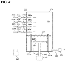
- the diamond film 210 can be grown, for example, using a thermal filament CVD apparatus 300 illustrated in FIG. 4 .
- the thermal filament CVD apparatus 300 includes an airtight container 303 which comprises a heat-resistant material such as quartz and in which a growth chamber 301 is constructed.
- a susceptor 308 for holding the substrate 220A is provided in the growth chamber 301.
- the susceptor 308 is connected to a rotation shaft 315 included in a rotation mechanism 316, and is rotatably configured.
- a gas supply pipe 332a for supplying nitrogen (N 2 ) gas into the growth chamber 301, a gas supply pipe 332b for supplying hydrogen (H 2 ) gas, a gas supply pipe 332c for supplying methane (CH 4 ) gas or ethane (C 2 H 6 ) gas as a carbon-containing gas, and a gas supply pipe 332d for supplying trimethylboron (B(CH 3 ) 3 , abbreviated as TMB) gas, trimethyl borate (B(OCH 3 ) 3 ) gas, triethyl borate (B(C 2 H 5 O) 3 ) gas, or diborane (B 2 H 6 ) gas as a boron-containing gas.
- TMB trimethylboron
- B(OCH 3 ) 3 trimethyl borate
- B(C 2 H 5 O) 3 triethyl borate
- diborane (B 2 H 6 ) gas as a boron-containing gas.
- To the gas supply pipes 332a to 332d are respectively provided flowrate controllers 341a to 341d and valves 343a to 343d in order from the upstream side of the gas flow.
- To downstream ends of the gas supply pipes 332a to 332d are respectively connected nozzles 349a to 349d for supplying gas supplied through the gas supply pipes 332a to 332d into the growth chamber 301.
- To another sidewall of the airtight container 303 is provided an exhaust pipe 330 for exhausting the growth chamber 301.
- To the exhaust pipe 330 is provided a pump 331.
- a temperature sensor 309 for measuring a temperature in the growth chamber 301.
- a tungsten filament 310 In the airtight container 303 are provided a tungsten filament 310, and a pair of electrodes (e.g., copper electrodes) 311a, 311b for heating the tungsten filament 310.
- Each member included in the thermal filament CVD apparatus 300 is connected to a controller 380 configured as a computer, and is configured so that processing procedures and processing conditions mentioned later are controlled with a program executed on the controller 380.
- the diamond film 210 is grown using the above-mentioned thermal filament CVD apparatus, for example, according to the following processing procedures.
- the substrate 220A is loaded (installed) in the airtight container 303, and held on the susceptor 308.
- H 2 -gas (or a mixed gas of N 2 -gas and H 2 -gas) is supplied into the growth chamber 301 while exhausting the growth chamber 301.
- a current is flowed between the electrodes 311a and 311b to start heating of the tungsten filament 310.
- the substrate 220A held on the susceptor 308 is also heated.
- CH 4 -gas and TMB-gas are supplied into the growth chamber 301.
- CH 4 -gas and TMB-gas supplied into the growth chamber 301 pass through the tungsten filament 310 heated to an elevated temperature, they are decomposed (thermally decomposed) to generate active species such as methyl radicals (CH 3 ⁇ ).
- active species such as methyl radicals (CH 3 ⁇ ).
- these active species and the like are supplied on the substrate 220A, the diamond film grows.
- the following conditions are exemplified as the conditions for growing the diamond film 210.
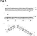
- the substrate 220A and the diamond film 210 illustrated in a schematic cross-sectional view in FIG. 5(a) there is produced a stack 230 including the substrate 220A and the diamond film 210 illustrated in a schematic cross-sectional view in FIG. 5(a) .
- the grown diamond film 210 is a poly-crystal diamond film.
- the thickness of the diamond film 210 becomes, for example, 0.5 ⁇ m or more and 10 ⁇ m or less, preferably 2 ⁇ m or more and 4 ⁇ m or less
- the B-concentration in the diamond film 210 becomes, for example, 1 ⁇ 10 19 cm -3 or more and 1 ⁇ 10 22 cm -3 or less.
- the concave grooves 222 are formed from a rear surface side of the stack 230 (a main surface side opposite to the first main surface 221 of the substrate 220A), as illustrated in FIG. 5(b) .
- the concave grooves 222 can be formed, for example, by laser scribing.
- the concave grooves 222 are provided so as to penetrate the substrate 220A in the thickness direction and reach the diamond film 210. Thereby, in the diamond film 210, a surface in contact with the substrate 220A is also irradiated with a laser. Therefore, in the diamond film 210, the alteration layer 211 is formed on the surface in contact with the substrate 220A.
- the diamond film 210 is broken along the concave grooves 222, as illustrated in FIG. 5(c) .
- the diamond film 210 is preferably bent outward along the concave grooves 222 to break.
- the broken surface may be formed on the side surface of the support 220 closer to the surface (first surface Si) in contact with the diamond film 210. That is, the side surface of the support 220 may have at least one selected from a group of the scribed surface and the etched surface generated by forming the concave grooves 222, and may also have the broken surface generated by breaking the substrate 220A along the concave grooves 222.
- the broken surface of the support 220 may include a cleaved surface.
- the alteration layer 211 is not formed on the surface in contact with the support 220 in the diamond film 210.
- Such an electrode 200 can be produced by forming the concave grooves 222 so as not to penetrate the substrate 220A in the thickness direction (so as not to reach the diamond film 210) in the above-mentioned formation of the concave grooves.
- the concave grooves 222 are preferably formed so that a thickness of the thinnest part of the substrate 220A is, for example, 10 ⁇ m or more and 80 ⁇ m or less. Thereby, a reduction in the breakage controllability of the diamond film 210 can be suppressed while suppressing a formation of the alteration layer 211.
- the alteration layer 211 is not formed on the diamond film 210, an adhesion between the support 220 and the diamond film 210 can be enhanced, as compared to a case where the alteration layer 211 is formed. Therefore, a life of the electrode 200 can be further extended, and the sensor performance of the sensor 100 using the electrode 200 can be reliably improved. Further, since the alteration layer 211 is not formed, variations in quality (e.g., electrical characteristics) of the diamond film 210 among a plurality of electrodes 200, can also be suppressed.
- the liquid test sample may be, in place of urine, blood, tear, snivel, saliva, sweat, or the like.
- the detected component may be a component other than uric acid.
- a predetermined enzyme corresponding to the detected component may be applied on the diamond film 210, the detected component such as uric acid and the enzyme may be electrochemically reacted, and the concentration of the detected component may be calculated.
- the concentration of the predetermined component in the liquid test sample is measured by the three-electrode method, but the present disclosure is not limited thereto.
- the concentration of the predetermined component in the liquid test sample may be measured by a two-electrode method.
- the sensor 100 may have structures similar to those in the above-mentioned embodiment except that the reference electrode 13 and the third wiring 33 are not provided.
- the test sample is supplied to the surface of the electrode group 10 through the water absorption member 40, but the present disclosure is not limited thereto.
- the sensor 100 does not have to include the water absorption member 40, and may be configured so that the test sample is directly supplied to the surface of the electrode group 10.
- the test sample may be a mist-like test sample, in place of the liquid test sample.
- the sensor 100 include one electrode group 10, but the sensor 100 may include a plurality of the electrode groups 10.
- the first to third wirings 31 to 33 are connected to each of the electrodes.
- first surface S 1 and the second surface S 2 of the support 220 are square in planar shape, but the present disclosure is not limited thereto.
- the first surface S 1 and the second surface S 2 of the support 220 may be, for example, rectangular other than square, or circular, in planar shape.
- explanation has been given for a case where the first surface S 1 and the second surface S 2 are similar in planar shape, but the present disclosure is not limited thereto.
- the first surface S 1 and the second surface S 2 may be non-similar.
- the first surface S 1 of the support 220 may be circular in planar shape
- the second surface S 2 of the support 220 may be square in planar shape.
- an electrochemical sensor unit including:
- an electrochemical sensor unit including:
- the sensor unit according to the supplementary description 1 or 2,
- the sensor unit according to any one of the supplementary descriptions 1 to 3,
- the sensor unit according to the supplementary description 4, wherein the side surface of the support comprises (consists of) one of the scribed surface and the etched surface.
- the sensor unit according to the supplementary description 5, wherein in the diamond film, an alteration layer is formed at an edge of a surface in contact with the support.
- the alteration layer is formed over an entire periphery of the edge of the surface in contact with the support.
- the sensor unit according to the supplementary description 4, wherein a broken surface generated by breaking the support along the concave grooves is formed on the side surface of the support closer to the surface in contact with the diamond film.
- the sensor unit according to the supplementary description 7, wherein in the diamond film, an alteration layer is not formed on a surface in contact with the support.
- the sensor unit according to the supplementary descriptions 1 to 8, wherein the support comprises a single-crystal silicon or a poly-crystal silicon.
- an electrode for electrochemical sensor including:
- an electrode for electrochemical sensor including:
- the concave grooves are formed so as to reach the diamond film.
- the concave grooves are formed so as not to reach the diamond film.
Landscapes
- Chemical & Material Sciences (AREA)
- Life Sciences & Earth Sciences (AREA)
- Health & Medical Sciences (AREA)
- Chemical Kinetics & Catalysis (AREA)
- General Physics & Mathematics (AREA)
- Electrochemistry (AREA)
- Physics & Mathematics (AREA)
- Analytical Chemistry (AREA)
- Biochemistry (AREA)
- General Health & Medical Sciences (AREA)
- Molecular Biology (AREA)
- Immunology (AREA)
- Pathology (AREA)
- Inorganic Chemistry (AREA)
- General Chemical & Material Sciences (AREA)
- Engineering & Computer Science (AREA)
- Materials Engineering (AREA)
- Mechanical Engineering (AREA)
- Metallurgy (AREA)
- Organic Chemistry (AREA)
- Investigating Or Analysing Biological Materials (AREA)
- Investigating Or Analyzing Materials By The Use Of Electric Means (AREA)
Abstract
Description
- The present disclosure relates to an electrochemical sensor unit, an electrode for electrochemical sensor, and a method of manufacturing an electrode for electrochemical sensor.
- Recently, it is proposed to use an electrode including a diamond film as a working electrode for an electrochemical sensor unit. Since conductive diamond has a wide potential window and a small background current, it enables electrochemical detection of various substances with high sensitivity. Therefore, conductive diamond is attracting attention as a material for the electrode for electrochemical sensor.
-
- Patent Document 1:
Japanese Patent Laid-Open Publication No. 2007-292717 - Patent Document 2:
Japanese Patent Laid-Open Publication No. 2013-208259 - An object of the present disclosure is to further improve a sensor performance of an electrochemical sensor unit including an electrode for electrochemical sensor, the electrode including a diamond film.
- According to an aspect of the present disclosure,
there is provided an electrochemical sensor unit and a related technique thereof, including: - a working electrode; and
- a counter electrode,
- wherein the working electrode includes a diamond film which generates a redox reaction on a surface when a voltage is applied between the working electrode and the counter electrode, and a support which is formed of a material different from diamond and supports the diamond film,
- when the working electrode is viewed laterally, in the support, a width of a surface opposite to a surface in contact with the diamond film is smaller than a width of the diamond film, and
- a liquid test sample is supplied to the working electrode from a diamond film side.
- According to the present disclosure, it is possible to further improve a sensor performance of an electrochemical sensor unit including an electrode for electrochemical sensor, the electrode including a diamond film.
-
-
FIG. 1 is a view illustrating an example of an exploded perspective view of an electrochemical sensor unit according to an embodiment of the present disclosure. -
FIG. 2 is a view illustrating an example of a cross-sectional structure of an electrode for electrochemical sensor according to the embodiment of the present disclosure. -
FIG. 3 is a view illustrating an example of a planar structure of the electrode for electrochemical sensor illustrated inFIG. 2 . -
FIG. 4 is a schematic view of a vapor phase deposition apparatus used to grow a diamond film. -
FIG. 5(a) is a cross-sectional view illustrating a stack including the diamond film and a substrate,FIG. 5(b) is a cross-sectional view illustrating a state where concave grooves (scribed grooves) are formed on a rear surface of the stack illustrated inFIG. 5(a), and FIG. 5(c) is a schematic view illustrating how the diamond film is broken along the concave grooves to obtain the electrode for electrochemical sensor. -
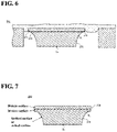
FIG. 6 is a cross-sectional view schematically illustrating an example of a main part while a water absorption member absorbs and retains a liquid test sample. -
FIG. 7 is a view illustrating an example of a cross-sectional structure of the electrode for electrochemical sensor according to a modified example of the embodiment of the present disclosure. - Explanation will be hereafter given for an electrochemical sensor unit which measures a concentration of a predetermined component in a liquid test sample by a three-electrode method as an embodiment of the present disclosure, with reference to
FIG. 1 . In the present embodiment, explanation will be given for an example of the electrochemical sensor unit which measures a uric acid concentration in urine by the three-electrode method. - As illustrated in
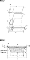
FIG. 1 , an electrochemical sensor unit 100 (hereafter also referred to as "sensor 100") according to the present embodiment includes: anelectrode group 10 constituted by a working electrode 11, acounter electrode 12, and a reference electrode 13; asupport member 20 which supports theelectrode group 10; first tothird wirings 31 to 33 connected to the working electrode 11, thecounter electrode 12, and the reference electrode 13, respectively; awater absorption member 40 arranged so as to cover theelectrode group 10; and awaterproof member 50 arranged so as to cover (a part of) the first tothird wirings 31 to 33. Thesensor 100 is configured to be disposable, for example. - The working electrode 11 includes a diamond film which generates on a surface thereof a redox reaction (electrochemical reaction) of a predetermined component (e.g., uric acid) in urine when applying a predetermined voltage between the working electrode 11 and the
counter electrode 12, both being in contact with a liquid test sample (e.g., urine), for example, using a measurement mechanism including a voltage applicator mentioned later. The details of the working electrode 11 will be mentioned later. - The
counter electrode 12 is an electrode for flowing a current generated by the above-mentioned redox reaction to the working electrode 11. As thecounter electrode 12, an electrode formed of metal such as platinum (Pt), gold (Au), copper (Cu), palladium (Pd), nickel (Ni), or silver (Ag), a carbon electrode, or the like can be used. - The reference electrode 13 is an electrode used as a basis for determining a potential of the working electrode 11. As the reference electrode 13, for example, a silver/silver chloride (Ag/AgCl) electrode can be used. As the reference electrode 13, a standard hydrogen electrode, a reversible hydrogen electrode, a palladium-hydrogen electrode, a saturated calomel electrode, or the like can also be used. As the reference electrode 13, an electrode formed of metal such as Pt, Au, Cu, Pd, Ni, or Ag, a carbon electrode, or the like can be used.
- In the present specification, the working electrode 11, the
counter electrode 12, and the reference electrode 13 are collectively referred to as theelectrode group 10 in some cases. - The
sensor 100 includes thesupport member 20 which supports theelectrode group 10. Theelectrode group 10 is arranged on the same surface of thesupport member 20. Thesupport member 20 is configured as a sheet-like (plate-like) base material, and has a size and shape (e.g., a rectangular (strip-like) planar shape) that is easy-to-handle (e.g., easy for a subject to grasp). Thesupport member 20 may include a longitudinal part (main part) and a convex part (a part connected to a measurement mechanism mentioned later). Thesupport member 20 has such a physical (mechanical) strength that it can be used as thesensor 100. For example, thesupport member 20 has such a strength that it does not bend nor break even when a test sample is attached thereto. Thesupport member 20 can be formed of insulating materials such as insulating composite resin, ceramic, glass, plastic, flammable materials, biodegradable materials, non-woven fabric, or paper. Thesupport member 20 is preferably a flexible base material. As thesupport member 20, for example, a base material formed of glass epoxy resin or polyethylene terephthalate (PET) can be suitably used. As thesupport member 20, a semiconductor base material or a metal base material can also be used which is configured so that its surface supporting theelectrode group 10 has an insulating property. The support member 20 (the longitudinal part thereof) may have a thickness of, for example, 200 µm or more and 1 mm or less, a width of, for example, 6 mm or more and 12 mm or less, and a length of, for example, 95 mm or more and 115 mm or less. In thesupport member 20 having the convex part, the convex part may have a length of, for example, 5 mm or more and 15 mm or less, and a width of 2 mm to 4 mm narrower than the width of the longitudinal part of thesupport member 20. - One end of the first wiring (conductor wiring) 31 is connected to the working electrode 11, one end of the second wiring (conductor wiring) 32 is connected to the
counter electrode 12, and one end of the third wiring (conductor wiring) 33 is connected to the reference electrode 13. Thefirst wiring 31 is electrically connected to the working electrode 11 via an anisotropic conductive film such as an ACF-film, a conductive paste such as a solder, metal, or the like. Thesecond wiring 32 and thecounter electrode 12 are integrally formed of the same material, and thethird wiring 33 and the reference electrode 13 are integrally formed of the same material. Thesecond wiring 32 and thecounter electrode 12 may be formed of different materials, and thethird wiring 33 and the reference electrode 13 may be formed of different materials. In this case, the second andthird wirings counter electrode 12 and the reference electrode 13, respectively, via an anisotropic conductive film, a conductive paste, or metal, similarly to thefirst wiring 31. - Each of the first to
third wirings 31 to 33 is arranged on the same surface as the surface of thesupport member 20 on which theelectrode group 10 is arranged. Each of the first tothird wirings 31 to 33 is preferably arranged so as to reach one end of thesupport member 20. Each of the first tothird wirings 31 to 33 can be formed, for example, using Cu. Each of the first tothird wirings 31 to 33 can be formed using, in place of Cu, a noble metal such as Au, Pt, Ag, or Pd; a metal such as aluminum (Al), iron (Fe), Ni, chromium (Cr), or titanium (Ti); an oxide of the above-mentioned noble metal or metal such as an alloy mainly containing the noble metal or metal; or the like. Each of the first tothird wirings 31 to 33 can also be formed using carbon. Each of the first tothird wirings 31 to 33 can be formed, for example, by a subtractive method in which an unnecessary part, not covered with resist, of a noble metal or metal film (e.g., Cu-film) previously adhered onto thesupport member 20 is removed by etching to form a necessary conductor pattern. For each of the first tothird wirings 31 to 33, the conductor pattern formed by the subtractive method may be, for example, Au-plated or Ag-plated. Each of the first tothird wirings 31 to 33 can be formed, for example, by a printing method, a vapor deposition method, or the like. An exemplary printing method is a screen printing method, a gravure printing method, an offset printing method, or an inkjet printing. - The
sensor 100 includes thewater absorption member 40 that absorbs and retains a supplied urine while bringing the retained urine into contact with a surface of theelectrode group 10. Thewater absorption member 40 is formed, for example, in a form of a sheet. Thewater absorption member 40 may have a thickness of, for example, 0.01 mm or more and 0.3 mm or less. - The
water absorption member 40 is arranged on thesupport member 20 so as to cover theelectrode group 10. Thewater absorption member 40 is arranged so as to come into contact with the surface of theelectrode group 10 when thewater absorption member 40 absorbs urine. Thewater absorption member 40 with no urine absorbed therein does not have to be in contact with the surface of theelectrode group 10. Thewater absorption member 40 is preferably arranged so as to prevent the absorbed urine from coming into contact with the first tothird wirings 31 to 33. - The
water absorption member 40 has anabsorption region 41 that absorbs and retains urine, at a position corresponding to theelectrode group 10 when thewater absorption member 40 is arranged. Thewater absorption member 40 preferably has anon-absorption region 42 that does not absorb urine and is provided so as to surround theabsorption region 41. Thereby, excess urine that is not in contact with theelectrode group 10 can be prevented from soaking into thewater absorption member 40. Also, urine can be reliably prevented from coming into contact with the first tothird wirings 31 to 33 through thewater absorption member 40. An entirety of thewater absorption member 40 may be theabsorption region 41, as long as thewater absorption member 40 is configured (arranged) so as to bring the absorbed urine into contact with the surface of theelectrode group 10 while preventing the absorbed urine from coming into contact with the first tothird wirings 31 to 33. - The
absorption region 41 can be formed, for example, using a natural fiber, a pulp fiber, a regenerated fiber, or a synthetic fiber. Specifically, theabsorption region 41 can be formed using a filter paper, a membrane filter, a glass filter, a filter cloth, or the like. Theabsorption region 41 can also be formed by letting an aggregate comprising the above-mentioned one or more fibers retain water-absorbing polymer grains or the like. Theabsorption region 41 may also be formed using a porous material such as a sponge or diatomaceous earth, a fiber material such as a non-woven fabric, or the like. - The
non-absorption region 42 can be formed of a water repellent or water-impermeable material. Thenon-absorption region 42 can be formed, for example, using plastic, silicon resin, Teflon (registered trademark) resin, or rubber. - The
sensor 100 includes thewaterproof member 50 which prevents urine from contacting with the first tothird wirings 31 to 33. Thewaterproof member 50 is formed, for example, in a form of a sheet. Thewaterproof member 50 is provided on the same surface as the surface of thesupport member 20 on which theelectrode group 10 is arranged, so as to cover (a part of) the first tothird wirings 31 to 33. Thewaterproof member 50 may have a thickness of, for example, 0.01 mm or more and 0.3 mm or less. - The
waterproof member 50 is configured, for example, so as to expose (theabsorption region 41 of) thewater absorption member 40 located on theelectrode group 10. For example, thewaterproof member 50 has anopening 51 formed at a position corresponding to at least theabsorption region 41 when thewaterproof member 50 is arranged. - Further, the
waterproof member 50 is configured as follows: of the two ends of the first tothird wirings 31 to 33, each of the other ends, different from the one ends respectively connected to the working electrode 11, thecounter electrode 12, and the reference electrode 13, is exposed at one end of thesupport member 20. For example, thewaterproof member 50 is formed so that its longitudinal length L50 is shorter than a longitudinal length L20 of the support member 20 (L50 < L20). In a measurement of the uric acid concentration using thesensor 100, a connector of the measurement mechanism configured separately from thesensor 100 is connected to the exposed other ends of the first tothird wirings 31 to 33. The other ends of the first tothird wirings 31 to 33 are exposed so as to be covered with (the connector of) the measurement mechanism when the above-mentioned connector of the measurement mechanism is connected to the other ends of the first tothird wirings 31 to 33. - As mentioned above, the
waterproof member 50 is configured so as to cover a predetermined region of the surface of thesupport member 20 on which theelectrode group 10 is arranged. Such a predetermined region is a region except for a region for allowing thewater absorption member 40 located on theelectrode group 10 to be exposed, and also is a region with which urine can come into contact in a state where the connector is connected (e.g., in a nip state of the measurement mechanism). - The
waterproof member 50 is preferably formed of a water-impermeable and insulating material, from a viewpoint of preventing urine from contacting with the first tothird wirings 31 to 33. For example, thewaterproof member 50 can be formed using plastic, silicon resin, Teflon (registered trademark) resin, rubber, or the like. - A
waterproof member 52 may be provided between thewaterproof member 50 and the first tothird wirings 31 to 33 to prevent urine from contacting with the first tothird wirings 31 to 33. Thewaterproof member 52 is formed in a form of a film, for example, using a material similar to that of thewaterproof member 50. Thewaterproof member 52 is provided on thesupport member 20 so as to cover a region other than exposed parts of the first tothird wirings 31 to 33, that is, to seal a region other than the exposed parts of the first tothird wirings 31 to 33. Thereby, urine can be reliably prevented from contacting with the first tothird wirings 31 to 33. Thewaterproof member 52 is preferably provided so as to cover the region other than the exposed parts of the first to thethird wirings 31 to 33, but may be provided so as to cover at least a region other than the exposed part of thefirst wiring 31. Thewaterproof member 52 does not have to be provided so long as thenon-absorption region 42 of thewater absorption member 40 and thewaterproof member 50 can reliably prevent urine from contacting with the first tothird wirings 31 to 33. - Explanation will be given for a method of measuring the uric acid concentration in urine by performing an electrochemical measurement using the above-mentioned
electrochemical sensor unit 100. - The method of measuring the uric acid concentration using the
electrochemical sensor unit 100 includes: - supplying urine to the
electrode group 10 through thewater absorption member 40 after the connector of the measurement mechanism is connected to the other ends of the first tothird wirings 31 to 33 (Step 1); - applying a voltage between the working electrode 11 and the
counter electrode 12 while urine is in contact with the surface of theelectrode group 10 to generate a redox reaction (electrochemical reaction) of uric acid on a surface of the diamond film included in the working electrode 11, and measuring a current value generated by the redox reaction of uric acid (Step 2); - measuring a potential difference (voltage difference) between the working electrode 11 and the reference electrode 13 while urine is in contact with the surface of the electrode group 10 (Step 3); and
- determining the uric acid concentration based on the measured current value and the potential difference (Step 4).
- The connector of the measurement mechanism configured separately from the
sensor 100 is connected to the other ends of the first tothird wirings 31 to 33 of the sensor 100 (to parts of the first tothird wirings 31 to 33, which are exposed from the waterproof member 50). The measurement mechanism is configured so as to electrically connect the connector of the measurement mechanism and the first tothird wirings 31 to 33 by simply nipping the other ends of the first tothird wirings 31 to 33 together with thesupport member 20. The measurement mechanism may also be configured to have an inserting opening (slot) through which the other ends of the first tothird wirings 31 to 33 (convex parts) are inserted, and to electrically connect the connector of the measurement mechanism and the first tothird wirings 31 to 33 by simply inserting the other ends of the first tothird wirings 31 to 33 (convex parts) into the inserting opening. - The measurement mechanism includes a voltage applicator, an amperemeter, a potentiometer, a potential adjustor, a uric acid concentration calculator, a display, a wireless communicator, and a storage. The voltage applicator, the amperemeter, the potentiometer, the potential adjustor, the uric acid concentration calculator, the display, the wireless communicator, and the storage, included in the measurement mechanism, are connected to each other so as to enable mutual data exchange. The voltage applicator is configured so as to apply a voltage between the working electrode 11 and the
counter electrode 12 when a predetermined circuit is formed by connecting the connector to the other ends of the first tothird wirings 31 to 33. The amperemeter is configured so as to measure a current generated by the redox reaction of uric acid. The potentiometer is configured so as to measure the potential difference (voltage difference) between the working electrode 11 and the reference electrode 13. The potential adjustor is configured so as to keep a potential of the working electrode 11 constant with reference to a potential of the reference electrode 13, based on the potential difference measured with the potentiometer. The uric acid concentration calculator is configured so as to calculate (determine) the uric acid concentration, based on the current value measured with the amperemeter. The display is configured so as to display the uric acid concentration calculated with the uric acid concentration calculator. The wireless communicator is configured so as to transmit data such as a measured current value, or a calculated uric acid concentration to an external device (computer, etc.) which is wirelessly connected. The storage stores a program or the like that describes a voltage application procedure, a current value measurement procedure, a potential adjustment procedure, a uric acid concentration calculation procedure, a uric acid concentration display procedure, a data transmission procedure, or the like. By executing the program, each of the above-mentioned procedure can be executed. The measurement mechanism may be configured so as to store the measured current value, the calculated uric acid concentration, and the like in the storage. - After the measurement mechanism is connected to the
sensor 100, urine is supplied to thesensor 100. For example, a subject urinates onto theopening 51 of thewaterproof member 50 of the sensor 100 (thewater absorption member 40 exposed through theopening 51 of the waterproof member 50). - When urine is supplied to the
sensor 100, the urine is absorbed by thewater absorption member 40. The urine absorbed by thewater absorption member 40 penetrates theabsorption region 41 of thewater absorption member 40 and reaches the surface of theelectrode group 10, and the urine comes into contact with the surface of theelectrode group 10. - By applying a voltage between the working electrode 11 and the
counter electrode 12 using the measurement mechanism while the urine is in contact with the surface of theelectrode group 10, the redox reaction of uric acid is generated on the surface of the diamond film included in the working electrode 11. The generation of the redox reaction of uric acid causes a current (hereafter also referred to as "reaction current") to flow through the working electrode 11. The reaction current value is measured, for example, by cyclic voltammetry using the measurement mechanism. An exemplary cyclic voltammetry condition is as follows: Voltage range, 0 to 1 V; Sweep speed, 0.1 to 1 V/s. The reaction current value may be measured by a method such as square wave voltammetry (rectangular-wave voltammetry), differential pulse voltammetry, normal pulse voltammetry, or AC-voltammetry. The measured reaction current value may be transmitted via the wireless communicator to an external device configured as a computer. - The potential difference (voltage difference) between the working electrode 11 and the reference electrode 13 during the above-mentioned step 2, is measured using the measurement mechanism.
- For example, a cyclic voltammogram is obtained using the reaction current values measured in step 2, to obtain an oxidation peak current value. The uric acid concentration is calculated (determined) using the measurement mechanism, based on the obtained oxidation peak current value and the potential difference value measured in step 3. The present inventors confirmed that the reaction current value is correlated with the uric acid concentration in urine. Therefore, by obtaining a relationship between the reaction current value and the uric acid concentration in advance, the uric acid concentration can be determined based on the measured reaction current value. Subsequently, the calculated uric acid concentration is displayed on the display. The calculated uric acid concentration may be transmitted via the wireless communicator to the external device configured as a computer.
- Explanation will be given for the electrode for electrochemical sensor according to the present embodiment, with reference to
FIG. 2 andFIG. 3 . Anelectrode 200 for electrochemical sensor (hereafter also referred to as "electrode 200") according to the present embodiment can be suitably used as the working electrode 11 in the above-mentionedsensor 100. Hereafter, explanation will be given for an example in which theelectrode 200 is used as the above-mentioned working electrode 11. - As illustrated in
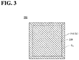
FIG. 2 , theelectrode 200 includes adiamond film 210 and asupport 220 that supports thediamond film 210, thediamond film 210 generating the redox reaction of uric acid on a surface thereof when applying a predetermined voltage to theelectrode 200 in contact with urine. In the above-mentionedsensor 100, theelectrode 200 is arranged on thesupport member 20 so that urine is supplied from thediamond film 210 side, that is, so that thediamond film 210 comes into contact with the above-mentionedwater absorption member 40. - The
diamond film 210 is a poly-crystal film. Thediamond film 210 preferably contains an element such as boron (B) at a concentration of, for example, 1 × 1019 cm-3 or more and 1 × 1022 cm-3 or less. B-concentration in thediamond film 210 can be measured, for example, by a secondary ion mass spectrometry (SIMS). Thediamond film 210 can be grown (synthesized) using a Chemical Vapor Deposition (CVD) method such as a thermal filament (hot filament) CVD method, a plasma CVD method; a Physical Vapor Deposition (PVD) method such as an ion beam method, an ionized deposition method; or the like. In the growth of thediamond film 210 using the thermal filament CVD method, as the filament, a tungsten filament can be used, for example. Thediamond film 210 may have a thickness of, for example, 0.5 µm or more and 10 µm or less, preferably 2 µm or more and 4 µm or less. - A side surface of the
diamond film 210 has a broken surface generated by breaking thediamond film 210 alongconcave grooves 222 mentioned later in a production of theelectrode 200. - In the
diamond film 210, analteration layer 211 is formed at an edge of a surface in contact with thesupport 220. In thediamond film 210, thealteration layer 211 is preferably formed over an entire periphery of the edge of the surface in contact with thesupport 220. The term "alteration layer" used herein refers to a layer formed by alteration (denaturation) of the diamond film 210 (crystal structure of diamond). For example, thealteration layer 211 refers to a layer formed as a result of a change of SP3-bonds to SP2-bonds in the diamond film 210 (i.e., a layer formed as a result of a graphitization of the diamond film 210) due to a laser irradiation, a layer formed as a result of an alteration of thediamond film 210 due to a mechanical machining, a bringing into contact with an etching liquid, a plasma irradiation, an ion beam irradiation, or the like. - The
support 220 is formed using a material (dissimilar material) different from diamond. As thesupport 220, a single-crystal silicon (Si) substrate can be used, for example. As thesupport 220, poly-crystal, a Si-substrate, a silicon carbide (SiC) substrate, or a metal substrate formed of a metal material such as stainless steel (SUS) can also be used. Thesupport 220 may have a thickness of, for example, 200 µm or more and 1000 µm or less. - The
support 220 is configured so that when the electrode 200 (a stack including thediamond film 210 and the support 220) is viewed laterally, in thesupport 220, a width W2 of a surface (hereafter also referred to as "second surface") S2 opposite to a surface in contact with thediamond film 210 is smaller than a width Wd of the diamond film 210 (W2 < Wd). That is, thesupport 220 has a side surface in which the width W2 of the second surface S2 is smaller than the width Wd of thediamond film 210. Since thesupport 220 has the above-mentioned configuration, a plane area of the second surface S2 of thesupport 220 is smaller than a plane area of thediamond film 210. - When the
electrode 200 is viewed laterally, in thesupport 220, the width W2 of the second surface S2 is preferably smaller than a width W1 of a surface (hereafter also referred to as "first surface") S1 in contact with thediamond film 210. That is, the plane area of the second surface S2 is preferably smaller than a plane area of the first surface S1. - When the
electrode 200 is viewed laterally, the width W1 of the first surface S1 is preferably substantially equal to the width Wd of thediamond film 210. A case of using the term "substantially equal to" includes, in addition to a case where the width W1 of the first surface S1 is exactly the same as the width Wd of thediamond film 210, a case where a difference between these widths is within 100 µm. More preferably, the width W1 of the first surface S1 is slightly smaller than the width Wd of thediamond film 210. - As illustrated in a planar view (top view) of the
electrode 200 inFIG. 3 , the first surface S1 and the second surface S2 are, for example, square in planar shape, and thesupport 220 has four side surfaces. All four side surfaces of thesupport 220 preferably have the above-mentioned configuration. That is, for all side surfaces of thesupport 220, the width W2 of the second surface S2 is preferably smaller than the width Wd of thediamond film 210, and more preferably smaller than the width Wd of thediamond film 210 and the width W1 of the first surface S1. - Each side surface of the
support 220 is an inclined surface that is gradually and gently curved from the first surface S1 to the second surface S2. Each side surface of thesupport 220 may be a flat inclined surface, for example. - As illustrated in
FIG. 2 , the side surface of thesupport 220 has at least one selected from a group of a scribed surface and an etched surface, generated by forming theconcave grooves 222 mentioned later in the production of theelectrode 200. The side surface of thesupport 220 preferably comprises (consists of) at least one selected from a group of the scribed surface and the etched surface. - The
concave grooves 222 can be formed using a known method such as laser machining, mechanical machining, or etching. The term "scribed surface" used herein refers to a surface, for example, including a molten surface (laser machined surface) formed by performing laser scribing (laser machining), or a cut surface (mechanical machined surface) formed by performing scribing (mechanical machining) using a diamond scriber or the like. The term "etched surface" used herein refers to a surface formed by wet etching, or etching using plasma or ion beam. - As illustrated in
FIG. 3 , when theelectrode 200 is viewed from thediamond film 210 side, it is preferable that thesupport 220 does not protrude from an outer periphery of thediamond film 210. That is, it is preferable that an outer periphery of the second surface S2 of thesupport 220 is located inside an outer periphery of the first surface S1 (diamond film 210), and the outer periphery of the first surface S1 overlaps or is located inside the outer periphery of thediamond film 210.FIG. 3 illustrates an example in which the outer periphery of the first surface S1 overlaps the outer periphery of thediamond film 210. In addition, it is more preferable that a center position of the first surface S1, a center position of the second surface S2, and a center position of thediamond film 210 coincide in a thickness direction of theelectrode 200. - Explanation will be given for a method of manufacturing the electrode for electrochemical sensor according to the
present embodiment 200, with reference toFIG. 4 andFIG. 5 . - First, a substrate (disk-shaped substrate) 220A is prepared which is formed of a material (dissimilar material) different from diamond, and has, for example, a circular outline in a planar view. For example, a disk-shaped
substrate 220A comprising a single-crystal Si is prepared. Thesubstrate 220A corresponds to thesupport 220 in theelectrode 200. - After the
substrate 220A is prepared, one main surface (hereafter also referred to as "firstmain surface 221") of two main surfaces of thesubstrate 220A is subjected to a seeding process, a scratching process, or the like. The seeding process refers to a process of attaching diamond grains onto the firstmain surface 221 of thesubstrate 220A by applying a solution (dispersion liquid) on the firstmain surface 221, or by immersing thesubstrate 220A in the dispersion liquid, the dispersion liquid being a liquid in which the diamond grains of, for example, about several nanometers to several tens micrometers disperse therein. The scratching process refers to a process of making scratches on the firstmain surface 221 using diamond abrasive grains (diamond powder) of about several micrometers, or the like. Thereby, thediamond film 210 can be grown on thesubstrate 220A. - After the
substrate 220A is prepared, thediamond film 210 is grown on the firstmain surface 221 of thesubstrate 220A, for example, by the thermal filament CVD method using the tungsten filament. - The
diamond film 210 can be grown, for example, using a thermalfilament CVD apparatus 300 illustrated inFIG. 4 . The thermalfilament CVD apparatus 300 includes anairtight container 303 which comprises a heat-resistant material such as quartz and in which agrowth chamber 301 is constructed. Asusceptor 308 for holding thesubstrate 220A is provided in thegrowth chamber 301. Thesusceptor 308 is connected to arotation shaft 315 included in arotation mechanism 316, and is rotatably configured. To a sidewall of theairtight container 303 are connected agas supply pipe 332a for supplying nitrogen (N2) gas into thegrowth chamber 301, agas supply pipe 332b for supplying hydrogen (H2) gas, agas supply pipe 332c for supplying methane (CH4) gas or ethane (C2H6) gas as a carbon-containing gas, and agas supply pipe 332d for supplying trimethylboron (B(CH3)3, abbreviated as TMB) gas, trimethyl borate (B(OCH3)3) gas, triethyl borate (B(C2H5O)3) gas, or diborane (B2H6) gas as a boron-containing gas. To thegas supply pipes 332a to 332d are respectively providedflowrate controllers 341a to 341d andvalves 343a to 343d in order from the upstream side of the gas flow. To downstream ends of thegas supply pipes 332a to 332d are respectively connectednozzles 349a to 349d for supplying gas supplied through thegas supply pipes 332a to 332d into thegrowth chamber 301. To another sidewall of theairtight container 303 is provided anexhaust pipe 330 for exhausting thegrowth chamber 301. To theexhaust pipe 330 is provided apump 331. In theairtight container 303 is provided atemperature sensor 309 for measuring a temperature in thegrowth chamber 301. In theairtight container 303 are provided atungsten filament 310, and a pair of electrodes (e.g., copper electrodes) 311a, 311b for heating thetungsten filament 310. Each member included in the thermalfilament CVD apparatus 300 is connected to acontroller 380 configured as a computer, and is configured so that processing procedures and processing conditions mentioned later are controlled with a program executed on thecontroller 380. - The
diamond film 210 is grown using the above-mentioned thermal filament CVD apparatus, for example, according to the following processing procedures. First, thesubstrate 220A is loaded (installed) in theairtight container 303, and held on thesusceptor 308. Then, H2-gas (or a mixed gas of N2-gas and H2-gas) is supplied into thegrowth chamber 301 while exhausting thegrowth chamber 301. A current is flowed between theelectrodes tungsten filament 310. As thetungsten filament 310 is heated, thesubstrate 220A held on thesusceptor 308 is also heated. After thetungsten filament 310 reaches a desired temperature, and a pressure in thegrowth chamber 301 reaches a desired growth pressure, and an atmosphere in thegrowth chamber 301 becomes a desired atmosphere, CH4-gas and TMB-gas are supplied into thegrowth chamber 301. As CH4-gas and TMB-gas supplied into thegrowth chamber 301 pass through thetungsten filament 310 heated to an elevated temperature, they are decomposed (thermally decomposed) to generate active species such as methyl radicals (CH3 ∗). As these active species and the like are supplied on thesubstrate 220A, the diamond film grows. - The following conditions are exemplified as the conditions for growing the
diamond film 210. - Substrate temperature: 600 °C or more and 1000 °C or less, preferably, 650 °C or more and 800 °C or less
- Filament temperature: 1800 °C or more and 2500 °C or less, preferably, 2000 °C or more and 2200 °C or less
- Pressure in growth chamber: 5 Torr or more and 50 Torr or less, preferably 10 Torr or more and 35 Torr or less
- Ratio of partial pressure of CH4-gas relative to partial pressure of TMB-gas (TMB / CH4): 0.003 % or more and 0.8 % or less
- Ratio of H2-gas relative to CH4-gas (CH4 / H2): 2 % or more and 5 % or less
- Thereby, there is produced a
stack 230 including thesubstrate 220A and thediamond film 210 illustrated in a schematic cross-sectional view inFIG. 5(a) . When thediamond film 210 is grown on thesubstrate 220A formed of a material different from diamond, the growndiamond film 210 is a poly-crystal diamond film. Further, when thediamond film 210 is grown under the above-mentioned conditions, the thickness of thediamond film 210 becomes, for example, 0.5 µm or more and 10 µm or less, preferably 2 µm or more and 4 µm or less, and the B-concentration in thediamond film 210 becomes, for example, 1 × 1019 cm-3 or more and 1 × 1022 cm-3 or less. - After the growth of the
diamond film 210 is completed, the concave grooves 222 (e.g., scribed grooves) are formed from a rear surface side of the stack 230 (a main surface side opposite to the firstmain surface 221 of thesubstrate 220A), as illustrated inFIG. 5(b) . Theconcave grooves 222 can be formed, for example, by laser scribing. Theconcave grooves 222 are provided so as to penetrate thesubstrate 220A in the thickness direction and reach thediamond film 210. Thereby, in thediamond film 210, a surface in contact with thesubstrate 220A is also irradiated with a laser. Therefore, in thediamond film 210, thealteration layer 211 is formed on the surface in contact with thesubstrate 220A. - After the
concave grooves 222 are formed, thediamond film 210 is broken along theconcave grooves 222, as illustrated inFIG. 5(c) . In this event, thediamond film 210 is preferably bent outward along theconcave grooves 222 to break. Thereby, there can be obtained the above-mentionedelectrode 200 including thediamond film 210 and thesupport 220. - According to the present embodiment, one or more of the following effects can be obtained.
- (a) Since the
electrode 200 including thesupport 220 in which the width W2 of the surface (second surface S2) opposite to the surface in contact with thediamond film 210 is smaller than the width Wd of thediamond film 210, is used as the working electrode 11 of theelectrochemical sensor unit 100, urine is less likely to come into contact with (attach to) the side surface of thesupport 220 when the urine is supplied from thediamond film 210 side. For example, as illustrated inFIG. 6 , even when urine is supplied to thesensor 100, and thewater absorption member 40 absorbs and retains the urine and swells, thewater absorption member 40 is less likely to come into contact with the side surface of thesupport 220. Therefore, it is possible to suppress the generation of the unintended redox reaction on the side surface of thesupport 220. Thereby, it is possible to suppress a current flowing through the working electrode 11 from being mixed with a current other than a current generated by the redox reaction of uric acid. For example, only the current generated by the redox reaction of uric acid can be the current flowing through the working electrode 11. As a result, a sensor performance of theelectrochemical sensor unit 100 can be improved. - (b) Since the
electrode 200 in which urine is less likely to come into contact with the side surface of thesupport 220 as mentioned above is used as the working electrode 11, it is not necessary to provide a layer for preventing urine from contacting with the side surface of thesupport 220. - (c) Since the outer periphery of the first surface S1 of the
support 220 overlaps or is located inside the outer periphery of thediamond film 210, it is possible to suppress urine from coming into contact with the first surface S1 of thesupport 220 when the urine comes into contact with the working electrode 11 through thewater absorption member 40. As a result, it is possible to suppress the generation of the unintended redox reaction on the first surface S1 of thesupport 220. Thereby, it is possible to reliably suppress the current flowing through the working electrode 11 from being mixed with a current other than a current generated by the redox reaction of uric acid. Therefore, the sensor performance of theelectrochemical sensor unit 100 can be reliably improved. - (e) The
electrode 200 is produced by growing thediamond film 210 on the firstmain surface 221 ofsubstrate 220A to produce thestack 230, then forming theconcave grooves 222 from the rear surface side of thestack 230, and breaking thediamond film 210 along theconcave grooves 222. As a result, it is possible to suppress thediamond film 210 from being peeled from thesubstrate 220A when thediamond film 210 is broken. For example, in the producedelectrode 200, an area of thediamond film 210 peeled from thesupport 220 can be, for example, 5 % or less. Thereby, a life of theelectrode 200 can be extended, and the sensor performance of theelectrochemical sensor unit 100 using theelectrode 200 can be improved. - (f) Further, by producing the
electrode 200 according to the above-mentioned procedure, theelectrode 200 having a predetermined shape can be easily produced even when theelectrode 200 includes thediamond film 210 having a high hardness.
It is also conceivable to form theconcave grooves 222 from a front surface side (thediamond film 210 side) of thestack 230 including thesubstrate 220A and thediamond film 210. However, since thediamond film 210 is a very hard film, it is difficult to form theconcave grooves 222 from thediamond film 210 side by laser machining or mechanical machining. Therefore, in this case, it is difficult to produce theelectrode 200 having a predetermined shape. - (g) In the production of the
electrode 200, by forming theconcave grooves 222 so as to penetrate thesubstrate 220A in the thickness direction to reach thediamond film 210, thealteration layer 211 can be formed on the surface in contact with thesubstrate 220A of thediamond film 210. Since thealteration layer 211 has a lower hardness and is more fragile compared to thediamond film 210, a breakage controllability of thediamond film 210 can be improved by forming thealteration layer 211. For example, when thediamond film 210 is broken, thediamond film 210 can be easily and accurately broken. - The above-mentioned embodiment can be modified as in the following modified example.
- As illustrated in
FIG. 7 , in theelectrode 200, the broken surface may be formed on the side surface of thesupport 220 closer to the surface (first surface Si) in contact with thediamond film 210. That is, the side surface of thesupport 220 may have at least one selected from a group of the scribed surface and the etched surface generated by forming theconcave grooves 222, and may also have the broken surface generated by breaking thesubstrate 220A along theconcave grooves 222. The broken surface of thesupport 220 may include a cleaved surface. In the present modified example, thealteration layer 211 is not formed on the surface in contact with thesupport 220 in thediamond film 210. Such anelectrode 200 can be produced by forming theconcave grooves 222 so as not to penetrate thesubstrate 220A in the thickness direction (so as not to reach the diamond film 210) in the above-mentioned formation of the concave grooves. In this case, theconcave grooves 222 are preferably formed so that a thickness of the thinnest part of thesubstrate 220A is, for example, 10 µm or more and 80 µm or less. Thereby, a reduction in the breakage controllability of thediamond film 210 can be suppressed while suppressing a formation of thealteration layer 211. - In the present modified example, since the
alteration layer 211 is not formed on thediamond film 210, an adhesion between thesupport 220 and thediamond film 210 can be enhanced, as compared to a case where thealteration layer 211 is formed. Therefore, a life of theelectrode 200 can be further extended, and the sensor performance of thesensor 100 using theelectrode 200 can be reliably improved. Further, since thealteration layer 211 is not formed, variations in quality (e.g., electrical characteristics) of thediamond film 210 among a plurality ofelectrodes 200, can also be suppressed. - Explanations have been given specifically for the embodiment of the present disclosure. However, the present disclosure is not limited to the above-mentioned embodiment, and can be variously modified in a range not departing from the gist of the disclosure.
- In the above-mentioned embodiment, explanation has been given for a case where the uric acid concentration in urine as a liquid test sample is measured, but the present disclosure is not limited thereto. The liquid test sample may be, in place of urine, blood, tear, snivel, saliva, sweat, or the like. The detected component may be a component other than uric acid. By appropriately changing the conditions of cyclic voltammetry, the concentrations of various components (substances) in the liquid test sample can be measured.
- A predetermined enzyme corresponding to the detected component may be applied on the
diamond film 210, the detected component such as uric acid and the enzyme may be electrochemically reacted, and the concentration of the detected component may be calculated. - In the above-mentioned embodiment, explanation has been given for a case where the concentration of the predetermined component in the liquid test sample is measured by the three-electrode method, but the present disclosure is not limited thereto. For example, the concentration of the predetermined component in the liquid test sample may be measured by a two-electrode method. In this case, the
sensor 100 may have structures similar to those in the above-mentioned embodiment except that the reference electrode 13 and thethird wiring 33 are not provided. - In the above-mentioned embodiment, explanation has been given for a case where the test sample is supplied to the surface of the
electrode group 10 through thewater absorption member 40, but the present disclosure is not limited thereto. For example, thesensor 100 does not have to include thewater absorption member 40, and may be configured so that the test sample is directly supplied to the surface of theelectrode group 10. In this case, the test sample may be a mist-like test sample, in place of the liquid test sample. - In the above-mentioned embodiment, explanation has been given for a case where the
sensor 100 include oneelectrode group 10, but thesensor 100 may include a plurality of the electrode groups 10. When a plurality of theelectrode groups 10 are included, the first tothird wirings 31 to 33 are connected to each of the electrodes. - In the above-mentioned embodiment, explanation has been given for a case where the first surface S1 and the second surface S2 of the
support 220 are square in planar shape, but the present disclosure is not limited thereto. The first surface S1 and the second surface S2 of thesupport 220 may be, for example, rectangular other than square, or circular, in planar shape. In the above-mentioned embodiment, explanation has been given for a case where the first surface S1 and the second surface S2 are similar in planar shape, but the present disclosure is not limited thereto. The first surface S1 and the second surface S2 may be non-similar. For example, the first surface S1 of thesupport 220 may be circular in planar shape, and the second surface S2 of thesupport 220 may be square in planar shape. - Preferable aspects of the present disclosure will be supplementarily described hereafter.
- According to an aspect of the present disclosure,
there is provided an electrochemical sensor unit, including: - a working electrode; and
- a counter electrode,
- wherein the working electrode includes a diamond film which generates a redox reaction on a surface when a voltage is applied between the working electrode and the counter electrode, and a support which is formed of a material different from diamond and supports the diamond film,
- when the working electrode is viewed laterally, in the support, a width of a surface opposite to a surface in contact with the diamond film is smaller than a width of the diamond film, and
- a liquid test sample is supplied to the working electrode from the diamond film side.
- According to another aspect of the present disclosure,
there is provided an electrochemical sensor unit, including: - a working electrode; and
- a counter electrode,
- wherein the working electrode includes a diamond film which generates a redox reaction on a surface when a voltage is applied between the working electrode and the counter electrode, and a support which is formed of a material different from diamond and supports the diamond film,
- in the support, a plane area of a surface opposite to a surface in contact with the diamond film is smaller than a plane area of the diamond film, and
- a liquid test sample is supplied to the working electrode from the diamond film side.
- Preferably, there is provided the sensor unit according to the supplementary description 1 or 2,
- wherein when the working electrode is viewed from the diamond film side, in the support, an outer periphery of the surface opposite to the surface in contact with the diamond film is located inside an outer periphery of the diamond film, and
- an outer periphery of the surface in contact with the diamond film overlaps or is located inside the outer periphery of the diamond film.
- Preferably, there is provided the sensor unit according to any one of the supplementary descriptions 1 to 3,
- wherein in the support, a side surface has at least one selected from a group of a scribed surface and an etched surface generated by forming concave grooves on the surface opposite to the surface in contact with the diamond film, and
- a side surface of the diamond film has a broken surface generated by breaking the diamond film along the concave grooves.
- Preferably, there is provided the sensor unit according to the supplementary description 4,
wherein the side surface of the support comprises (consists of) one of the scribed surface and the etched surface. - Preferably, there is provided the sensor unit according to the supplementary description 5,
wherein in the diamond film, an alteration layer is formed at an edge of a surface in contact with the support. - Preferably, in the diamond film, the alteration layer is formed over an entire periphery of the edge of the surface in contact with the support.
- Preferably, there is provided the sensor unit according to the supplementary description 4,
wherein a broken surface generated by breaking the support along the concave grooves is formed on the side surface of the support closer to the surface in contact with the diamond film. - Preferably, there is provided the sensor unit according to the supplementary description 7,
wherein in the diamond film, an alteration layer is not formed on a surface in contact with the support. - Preferably, there is provided the sensor unit according to the supplementary descriptions 1 to 8,
wherein the support comprises a single-crystal silicon or a poly-crystal silicon. - According to further another aspect of the present disclosure,
there is provided an electrode for electrochemical sensor, including: - a diamond film which generates a redox reaction on a surface when a voltage is applied; and
- a support which is formed of a material different from diamond and supports the diamond film,
- wherein when a stack including the diamond film and the support is viewed laterally, in the support, a width of a surface opposite to a surface in contact with the diamond film is smaller than a width of the surface in contact with the diamond film, and
- a liquid test sample is supplied from the diamond film side of the stack.
- According to further another aspect of the present disclosure,
there is provided a method of manufacturing an electrode for electrochemical sensor, including: - preparing a substrate comprising a material different from diamond;
- producing a stack by forming (depositing) a diamond film on one of two main surfaces of the substrate;
- forming concave grooves of a predetermined shape on a main surface of the substrate, the main surface being opposite to a main surface on which the diamond film is formed; and
- breaking the diamond film along the concave grooves.
- Preferably, there is provided the method according to the supplementary description 11,
wherein in the formation of the concave grooves, the concave grooves are formed so as to reach the diamond film. - Preferably, there is provided the method according to the supplementary description 11,
wherein in the formation of the concave grooves, the concave grooves are formed so as not to reach the diamond film. - Preferably, there is provided the method according to any one of the supplementary descriptions 11 to 13,
wherein in the breaking of the diamond film, the diamond film is bent outward along the concave grooves to break. -
- 100 Electrochemical sensor unit
- 11 Working electrode
- 200 Electrode for electrochemical sensor
- 210 Diamond film
- 220 Support
Claims (10)
- An electrochemical sensor unit, comprising:a working electrode; anda counter electrode,wherein the working electrode includes a diamond film which generates a redox reaction on a surface when a voltage is applied between the working electrode and the counter electrode, and a support which is formed of a material different from diamond and supports the diamond film,when the working electrode is viewed laterally, in the support, a width of a surface opposite to a surface in contact with the diamond film is smaller than a width of the diamond film, anda liquid test sample is supplied to the working electrode from the diamond film side.
- The electrochemical sensor unit according to claim 1,wherein when the working electrode is viewed from the diamond film side, in the support, an outer periphery of the surface opposite to the surface in contact with the diamond film is located inside an outer periphery of the diamond film, andan outer periphery of the surface in contact with the diamond film overlaps or is located inside the outer periphery of the diamond film.
- The electrochemical sensor unit according to claim 1 or 2,wherein in the support, a side surface has at least one selected from a group of a scribed surface and an etched surface generated by forming concave grooves on the surface opposite to the surface in contact with the diamond film, anda side surface of the diamond film has a broken surface generated by breaking the diamond film along the concave grooves.
- The electrochemical sensor unit according to claim 3,
wherein the side surface of the support comprises one of the scribed surface and the etched surface. - The electrochemical sensor unit according to claim 3,
wherein a broken surface generated by breaking the support along the concave grooves is formed on the side surface of the support closer to the surface in contact with the diamond film. - An electrode for electrochemical sensor, comprising:a diamond film which generates a redox reaction on a surface when a voltage is applied; anda support which is formed of a material different from diamond and supports the diamond film,wherein when a stack including the diamond film and the support is viewed laterally, in the support, a width of a surface opposite to a surface in contact with the diamond film is smaller than a width of the surface in contact with the diamond film, anda liquid test sample is supplied from the diamond film side of the stack.
- A method of manufacturing an electrode for electrochemical sensor, comprising:preparing a substrate comprising a material different from diamond;producing a stack by forming a diamond film on one of two main surfaces of the substrate;forming concave grooves of a predetermined shape on a main surface of the substrate, the main surface being opposite to a main surface on which the diamond film is formed; andbreaking the diamond film along the concave grooves.
- The method of manufacturing the electrode for electrochemical sensor according to claim 7,
wherein in the formation of the concave grooves, the concave grooves are formed so as to reach the diamond film. - The method of manufacturing the electrode for electrochemical sensor according to claim 7,
wherein in the formation of the concave grooves, the concave grooves are formed so as not to reach the diamond film. - The method of manufacturing the electrode for electrochemical sensor according to any one of claims 7 to 9,
wherein in the breaking of the diamond film, the diamond film is bent outward along the concave grooves to break.
Applications Claiming Priority (2)
| Application Number | Priority Date | Filing Date | Title |
|---|---|---|---|
| JP2019133226A JP7245738B2 (en) | 2019-07-19 | 2019-07-19 | Electrochemical sensor unit, electrochemical sensor electrode, and electrochemical sensor electrode manufacturing method |
| PCT/JP2020/027464 WO2021015067A1 (en) | 2019-07-19 | 2020-07-15 | Electrochemical sensor unit, electrode for electrochemical sensor, and method for manufacturing electrode for electrochemical sensor |
Publications (2)
| Publication Number | Publication Date |
|---|---|
| EP4001908A1 true EP4001908A1 (en) | 2022-05-25 |
| EP4001908A4 EP4001908A4 (en) | 2023-07-12 |
Family
ID=74193491
Family Applications (1)
| Application Number | Title | Priority Date | Filing Date |
|---|---|---|---|
| EP20843662.6A Withdrawn EP4001908A4 (en) | 2019-07-19 | 2020-07-15 | ELECTROCHEMICAL SENSOR UNIT, ELECTROCHEMICAL SENSOR ELECTRODE AND ELECTROCHEMICAL SENSOR ELECTRODE MANUFACTURING METHOD |
Country Status (6)
| Country | Link |
|---|---|
| US (1) | US12306130B2 (en) |
| EP (1) | EP4001908A4 (en) |
| JP (1) | JP7245738B2 (en) |
| CN (1) | CN114072664B (en) |
| TW (1) | TW202113350A (en) |
| WO (1) | WO2021015067A1 (en) |
Families Citing this family (9)
| Publication number | Priority date | Publication date | Assignee | Title |
|---|---|---|---|---|
| JP7547074B2 (en) * | 2020-04-23 | 2024-09-09 | 住友化学株式会社 | Electrochemical sensor and method for manufacturing the same |
| JP7637525B2 (en) * | 2021-02-12 | 2025-02-28 | 住友化学株式会社 | Chip-shaped electrode and method for manufacturing the electrode |
| CN113514523A (en) * | 2021-06-01 | 2021-10-19 | 广州大学 | Sweat detection method using an all-solid-state sweat sensor chip |
| JP7277529B2 (en) * | 2021-09-14 | 2023-05-19 | 住友化学株式会社 | electrochemical sensor |
| JP7293413B1 (en) | 2022-01-26 | 2023-06-19 | 住友化学株式会社 | LAMINATED STRUCTURE FOR ELECTRODE AND METHOD FOR MANUFACTURING LAMINATED STRUCTURE FOR ELECTRODE |
| JP2023142217A (en) * | 2022-03-24 | 2023-10-05 | 住友化学株式会社 | Electrode chips and electronic equipment |
| CN116288947B (en) * | 2023-03-21 | 2024-01-19 | 无锡爱勒普科技有限公司 | Composite non-woven fabric for screen printing and preparation method thereof |
| WO2025023224A1 (en) * | 2023-07-26 | 2025-01-30 | 株式会社ExtenD | Sensor, analysis device, terminal device, analysis system using these, and program to be executed by computer |
| JP7598188B1 (en) * | 2023-07-26 | 2024-12-11 | 株式会社ExtenD | Sensor, analysis device, terminal device, analysis system using these, and program for executing on a computer |
Family Cites Families (20)
| Publication number | Priority date | Publication date | Assignee | Title |
|---|---|---|---|---|
| JPWO2001098766A1 (en) | 2000-06-21 | 2004-07-15 | 株式会社先端科学技術インキュベーションセンター | Method for measuring the concentration of a xanthine compound and a sensor used therefor |
| EP1254972A1 (en) | 2001-05-01 | 2002-11-06 | CSEM Centre Suisse d'Electronique et de Microtechnique SA | Modular electrochemical cell |
| US7534296B2 (en) * | 2002-01-11 | 2009-05-19 | Board Of Trustees Of Michigan State University | Electrically conductive diamond electrodes |
| JP3703787B2 (en) | 2002-09-11 | 2005-10-05 | 独立行政法人科学技術振興機構 | Method for measuring analyte concentration using conductive diamond electrode and apparatus therefor |
| JP2004325384A (en) * | 2003-04-28 | 2004-11-18 | Matsushita Electric Ind Co Ltd | Biosensor |
| JP4877641B2 (en) * | 2004-08-31 | 2012-02-15 | 住友電気工業株式会社 | Diamond local wiring electrode |
| JP4348308B2 (en) | 2005-03-14 | 2009-10-21 | 住友電工ハードメタル株式会社 | Diamond electrode structure and manufacturing method thereof |
| EP1813937A1 (en) * | 2006-01-25 | 2007-08-01 | Roche Diagnostics GmbH | Electrochemical biosensor analysis system |
| JP4978858B2 (en) | 2006-03-29 | 2012-07-18 | 学校法人東京理科大学 | Diamond electrode and sensor equipped with the same |
| JP2009156572A (en) | 2006-04-06 | 2009-07-16 | National Institutes Of Natural Sciences | Ion channel protein biosensor |
| RU2357001C2 (en) * | 2007-07-25 | 2009-05-27 | Ооо "Твинн" | Method of products receiving from polycrystalline diamond |
| KR20110073461A (en) * | 2008-09-24 | 2011-06-29 | 쿠리타 고교 가부시키가이샤 | Diamond Electrode and Manufacturing Method of Diamond Electrode |
| GB201104579D0 (en) * | 2011-03-18 | 2011-05-04 | Element Six Ltd | Diamond based electrochemical sensors |
| JP4905904B2 (en) * | 2011-06-23 | 2012-03-28 | 株式会社神戸製鋼所 | Diamond electrode member |
| JP6009794B2 (en) | 2012-03-30 | 2016-10-19 | 学校法人慶應義塾 | Measuring apparatus for reduced glutathione using diamond microelectrodes |
| GB201214448D0 (en) | 2012-08-14 | 2012-09-26 | Element Six Ltd | Electrochemical deposition and x-ray fluorescence spectroscopy |
| JP5265803B1 (en) | 2012-11-16 | 2013-08-14 | 学校法人慶應義塾 | Ozone water concentration measuring device and ozone water concentration measuring method |
| JP6571534B2 (en) * | 2014-01-20 | 2019-09-04 | 住友化学株式会社 | Compound and electronic device |
| JP2018200248A (en) * | 2017-05-29 | 2018-12-20 | 凸版印刷株式会社 | Gas sensor and manufacturing method thereof |
| JP7302111B2 (en) * | 2019-07-19 | 2023-07-03 | 住友化学株式会社 | Electrodes for electrochemical sensors |
-
2019
- 2019-07-19 JP JP2019133226A patent/JP7245738B2/en active Active
-
2020
- 2020-07-06 TW TW109122735A patent/TW202113350A/en unknown
- 2020-07-15 WO PCT/JP2020/027464 patent/WO2021015067A1/en not_active Ceased
- 2020-07-15 US US17/628,037 patent/US12306130B2/en active Active
- 2020-07-15 EP EP20843662.6A patent/EP4001908A4/en not_active Withdrawn
- 2020-07-15 CN CN202080048028.6A patent/CN114072664B/en active Active
Also Published As
| Publication number | Publication date |
|---|---|
| US12306130B2 (en) | 2025-05-20 |
| TW202113350A (en) | 2021-04-01 |
| JP2021018122A (en) | 2021-02-15 |
| EP4001908A4 (en) | 2023-07-12 |
| CN114072664A (en) | 2022-02-18 |
| US20220260516A1 (en) | 2022-08-18 |
| CN114072664B (en) | 2024-07-30 |
| JP7245738B2 (en) | 2023-03-24 |
| WO2021015067A1 (en) | 2021-01-28 |
Similar Documents
| Publication | Publication Date | Title |
|---|---|---|
| US12306130B2 (en) | Electrochemical sensor unit, electrode for electrochemical sensor, and method of manufacturing electrode for electrochemical sensor | |
| EP4141431A1 (en) | Electrochemical sensor and method for producing electrochemical sensor | |
| Sobaszek et al. | Diamond phase (sp3-C) rich boron-doped carbon nanowalls (sp2-C): physicochemical and electrochemical properties | |
| EP2686672B1 (en) | Diamond based electrochemical sensors | |
| EP2825872A1 (en) | Synthetic diamond materials for electrochemical sensing applications | |
| JP5265803B1 (en) | Ozone water concentration measuring device and ozone water concentration measuring method | |
| JP7302111B2 (en) | Electrodes for electrochemical sensors | |
| EP4403910A1 (en) | Electrochemical sensor | |
| JP7345602B1 (en) | Electrochemical sensor and method for manufacturing electrochemical sensor | |
| US20250110075A1 (en) | Electrode-use stack structure and method of manufacturing electrode-use stack structure | |
| WO2023181833A1 (en) | Electrode chip and electronic device | |
| JP7637525B2 (en) | Chip-shaped electrode and method for manufacturing the electrode | |
| JP2023162596A (en) | Diamond electrode, electrochemical sensor unit, and diamond electrode manufacturing method | |
| CN115825180A (en) | Electrochemical sensor based on silicon carbide/graphene material and preparation method and application thereof | |
| Yang et al. | Investigation of the boron-doped CVD diamond films for use in sensors |
Legal Events
| Date | Code | Title | Description |
|---|---|---|---|
| STAA | Information on the status of an ep patent application or granted ep patent |
Free format text: STATUS: THE INTERNATIONAL PUBLICATION HAS BEEN MADE |
|
| PUAI | Public reference made under article 153(3) epc to a published international application that has entered the european phase |
Free format text: ORIGINAL CODE: 0009012 |
|
| STAA | Information on the status of an ep patent application or granted ep patent |
Free format text: STATUS: REQUEST FOR EXAMINATION WAS MADE |
|
| 17P | Request for examination filed |
Effective date: 20220219 |
|
| AK | Designated contracting states |
Kind code of ref document: A1 Designated state(s): AL AT BE BG CH CY CZ DE DK EE ES FI FR GB GR HR HU IE IS IT LI LT LU LV MC MK MT NL NO PL PT RO RS SE SI SK SM TR |
|
| DAV | Request for validation of the european patent (deleted) | ||
| DAX | Request for extension of the european patent (deleted) | ||
| A4 | Supplementary search report drawn up and despatched |
Effective date: 20230614 |
|
| RIC1 | Information provided on ipc code assigned before grant |
Ipc: G01N 27/30 20060101AFI20230607BHEP |
|
| STAA | Information on the status of an ep patent application or granted ep patent |
Free format text: STATUS: EXAMINATION IS IN PROGRESS |
|
| 17Q | First examination report despatched |
Effective date: 20250617 |
|
| STAA | Information on the status of an ep patent application or granted ep patent |
Free format text: STATUS: THE APPLICATION HAS BEEN WITHDRAWN |
|
| 18W | Application withdrawn |
Effective date: 20250722 |