EP3996295A1 - High-speed bidirectional optical time-domain reflectometer (otdr)-based testing of device under test - Google Patents
High-speed bidirectional optical time-domain reflectometer (otdr)-based testing of device under test Download PDFInfo
- Publication number
- EP3996295A1 EP3996295A1 EP21205999.2A EP21205999A EP3996295A1 EP 3996295 A1 EP3996295 A1 EP 3996295A1 EP 21205999 A EP21205999 A EP 21205999A EP 3996295 A1 EP3996295 A1 EP 3996295A1
- Authority
- EP
- European Patent Office
- Prior art keywords
- data
- receiver
- dut
- towards
- otdr
- Prior art date
- Legal status (The legal status is an assumption and is not a legal conclusion. Google has not performed a legal analysis and makes no representation as to the accuracy of the status listed.)
- Pending
Links
Images


Classifications
-
- H—ELECTRICITY
- H04—ELECTRIC COMMUNICATION TECHNIQUE
- H04B—TRANSMISSION
- H04B10/00—Transmission systems employing electromagnetic waves other than radio-waves, e.g. infrared, visible or ultraviolet light, or employing corpuscular radiation, e.g. quantum communication
- H04B10/07—Arrangements for monitoring or testing transmission systems; Arrangements for fault measurement of transmission systems
- H04B10/071—Arrangements for monitoring or testing transmission systems; Arrangements for fault measurement of transmission systems using a reflected signal, e.g. using optical time domain reflectometers [OTDR]
-
- H—ELECTRICITY
- H04—ELECTRIC COMMUNICATION TECHNIQUE
- H04B—TRANSMISSION
- H04B10/00—Transmission systems employing electromagnetic waves other than radio-waves, e.g. infrared, visible or ultraviolet light, or employing corpuscular radiation, e.g. quantum communication
- H04B10/25—Arrangements specific to fibre transmission
-
- H—ELECTRICITY
- H04—ELECTRIC COMMUNICATION TECHNIQUE
- H04B—TRANSMISSION
- H04B10/00—Transmission systems employing electromagnetic waves other than radio-waves, e.g. infrared, visible or ultraviolet light, or employing corpuscular radiation, e.g. quantum communication
- H04B10/50—Transmitters
-
- H—ELECTRICITY
- H04—ELECTRIC COMMUNICATION TECHNIQUE
- H04B—TRANSMISSION
- H04B10/00—Transmission systems employing electromagnetic waves other than radio-waves, e.g. infrared, visible or ultraviolet light, or employing corpuscular radiation, e.g. quantum communication
- H04B10/60—Receivers
- H04B10/66—Non-coherent receivers, e.g. using direct detection
- H04B10/67—Optical arrangements in the receiver
- H04B10/671—Optical arrangements in the receiver for controlling the input optical signal
- H04B10/672—Optical arrangements in the receiver for controlling the input optical signal for controlling the power of the input optical signal
- H04B10/674—Optical arrangements in the receiver for controlling the input optical signal for controlling the power of the input optical signal using a variable optical attenuator
-
- H—ELECTRICITY
- H04—ELECTRIC COMMUNICATION TECHNIQUE
- H04B—TRANSMISSION
- H04B10/00—Transmission systems employing electromagnetic waves other than radio-waves, e.g. infrared, visible or ultraviolet light, or employing corpuscular radiation, e.g. quantum communication
- H04B10/40—Transceivers
Definitions
- a fiber optic cable may include one or more optical fibers that may be used to transmit light from a source to a destination.
- the optical fibers of the fiber optic cable may be referred to as fiber optic links.
- Fiber optic cables may represent a network element of a fiber optic network.
- other types of network elements may include optical connectors, optical splices, optical couplers, and optical switches.
- a fiber optic network may be monitored, for example, by a remote fiber monitoring system that enables oversight of an entire fiber optic network from a central location.
- the terms “a” and “an” are intended to denote at least one of a particular element.
- the term “includes” means includes but not limited to, the term “including” means including but not limited to.
- the term “based on” means based at least in part on.
- High speed bidirectional Optical Time Domain Reflectometer (OTDR)-based testing apparatuses, methods for high speed bidirectional OTDR-based testing, and non-transitory computer readable media for high speed bidirectional OTDR-based testing are disclosed herein.
- the apparatuses, methods, and non-transitory computer readable media disclosed herein provide for relatively high test speeds, for example, for data transfers such as transfer of OTDR measurement point files, within a relatively short time duration.
- the apparatuses, methods, and non-transitory computer readable media disclosed herein provide for high-performance communication based on the implementation of hardware and software functionality that is dedicated to the transfer of data.
- an OTDR may utilize Rayleigh backscattering and Fresnel reflection signals to monitor events with respect to a fiber optic network.
- One of the unique advantages of OTDR testing is that it utilizes access to one end of a fiber optic cable that may include a plurality of fiber optic links. Since distance and attenuation measurements are based on Rayleigh optical backscattering and the Fresnel reflection principle, returned light may be analyzed directly from the one end of a fiber optic link of the fiber optic cable.
- two-way reflectometry test methods may be utilized to improve the precision and accuracy of testing of a fiber optic link.
- the two-way reflectometry test methods may be denoted as bidirectional reflectometry testing.
- a fiber optic link may be characterized by measuring attenuation and loss from both ends of the fiber optic link.
- Figures 2A and 2B illustrate testing of a fiber optic link (e.g., a device under test (DUT) as disclosed herein) in both directions by an OTDR, in accordance with an example of the present disclosure.
- a fiber optic link e.g., a device under test (DUT) as disclosed herein
- the fiber optic link 200 may be operatively connected to a launch fiber 202 and a receive fiber 204 at opposite ends thereof.
- the launch fiber 202 may be operatively connected to port of OTDR-1 at 206, and to a DUT that may include the fiber optic link 200.
- the launch fiber 202 may be used to interface the OTDR-1 with the fiber optic link 200 in order to limit the risk of damage to the optical connector of the OTDR-1 by reducing the number of optical connections and disconnections.
- the launch and receive fibers may also provide for full characterization of the end connections of the fiber optic link 200.
- the launch and receive fibers may create a symmetrical configuration at both ends of the fiber optic link 200.
- the same fiber optic link 200 may be tested in both directions using one or two OTDRs (e.g., OTDR-1 at 206 of Figure 2A , and OTDR-2 at 208 of Figure 2B ). The average of the results obtained in both directions may then be determined.
- bidirectional fiber optic link testing may provide higher accuracy results with respect to characterization of the fiber optic link.
- Rayleigh backscatter is used to quantify the fiber optic link attenuation and insertion loss of each event
- the fiber optic link backscatter coefficient may need to be known and programmed into the OTDR. This coefficient can vary between different fiber optic links, and the OTDR may display excessive attenuation or even negative attenuation (e.g., gain) at the junctions between fiber optic links with different coefficients.
- the actual value of the fiber optic link attenuation and of each event during the presence of fibers with different coefficients on the same fiber optic link may be determined by averaging the results obtained with a bidirectional OTDR test.
- the splice attenuation measured by the OTDR may be negative (e.g., therefore false). This effect may be designated as a "gain" because the amount of backscatter observed may be higher after the event than before. Conversely, if a fiber optic link with a higher backscatter coefficient has been soldered to a fiber optic link with a lower backscatter coefficient, the splice attenuation measured by the OTDR may be greater than the actual attenuation of that splice. By averaging the values obtained from the two ends of the fiber optic link, the actual value of the attenuation of a splice or connection may be obtained.
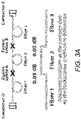
- Figures 3A-3B illustrate a principle of reducing insertion loss measurement errors related to a difference in Rayleigh backscattering coefficients between fiber optic links, and a combination of the curves or the measurement results of the measurements carried out in both directions, in accordance with an example of the present disclosure.
- Figure 3A shows the principle of reducing insertion loss measurement errors related to the difference in Rayleigh backscattering coefficients between fiber optic link-2 (e.g., Fiber-2), and fiber optic link-1 and fiber optic link-3 (e.g., Fiber-1 and Fiber 3).
- Fiber-1, Fiber-2, and Fiber-3 may be respectively connected at Splice-A and Splice-B, with a 0.05 dB apparent loss/gain at the junctions of the splices.
- Figures 3B and 3C respectively illustrate the combination of curves or measurement results of the measurements performed in both directions.
- Figures 3B and 3C provide for the apparent loss values to be obtained.
- the half-sum of the insertion losses may be obtained on both sides of the fiber optic link to remove the influence of the relative Rayleigh backscattering coefficients.
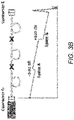
- Figure 4 illustrates half-sum of the insertion losses obtained on both sides for the fiber optic links of Figures 3A-3C to remove the influence of the relative Rayleigh backscattering coefficients, in accordance with an example of the present disclosure.
- Figure 4 provides examples of half-sum determination, where the values 0-> E and E->0 may be added and then divided by two.
- an OTDR such as OTDR-1 may be connected to one end of a fiber optic link to perform a measurement in one direction, and the same OTDR may be disconnected and connected to an opposite end of the fiber optic link to perform a second measurement in an opposite direction.
- bidirectional reflectometry techniques as illustrated in Figure 2C , which may be referred to as automated bidirectional reflectometry techniques, by pairing a local OTDR with a far end OTDR connected at the opposite end of the fiber optic link (e.g., or a fiber optic cable including the fiber optic link), communication between the two OTDRs will ensure identical test configurations, continuity of the fiber link, and easier acquisition and compilation of data.
- the measurement time may also be reduced while ensuring the quality of the measurements and reducing the risk of errors.
- the automated functionality may be used to perform reflectometry tests at multiple wavelengths (e.g., to improve detection of fiber optic link bends), and include bidirectional attenuation and optical reflection loss (ORL) tests.
- a loopback cable may connect one fiber optic link to another fiber optic link which is also to be tested.
- an OTDR test pulse may be sent down one fiber optic link and continues through the loop back and down the second fiber optic link, thus testing both fibers uni-directionally at the same time.
- both fiber optic links may then be tested in the opposite direction from the same location.
- This technique may use an OTDR approach such as where a single OTDR is moved from the first to the second fiber optic link to manually test in each direction and the results may be manually combined, or an automated OTDR approach where two OTDRs are used, one connected to each fiber optic link end to automatically test each direction and combine test results.
- multipurpose OTDRs and testers may be configured for automated bidirectional reflectometry or other bidirectional fiber optic testing, at the push of a button. These devices may also include a built-in feature that allows them to generate reports for speed and convenience.
- the test instruments e.g., OTDRs
- the test instruments may need to exchange data to synchronize the measurement, exchange setup information, and exchange results.
- the OTDR devices may implement frequency modulation to exchange data. Each synchronization, events and measurement results may be encoded by a frequency. However, this process of sending and decoding data may include a plurality of sequences of data exchange. In this regard, it is technically challenging to further reduce a time needed to exchange data between two or more test instruments (e.g., OTDRs).
- test instruments e.g., OTDRs
- the apparatuses, methods, and non-transitory computer readable media disclosed herein address the aforementioned technical challenges by providing for relatively high test speeds, for example, for data transfers such as transfer of OTDR measurement point files, within a relatively short time duration.
- the apparatuses, methods, and non-transitory computer readable media disclosed herein provide for high-performance communication based on the implementation of hardware and software functionality that is dedicated to the transfer of data.
- the apparatuses, methods, and non-transitory computer readable media disclosed herein provide for utilization of an OTDR and the DUT (e.g., a fiber optic link) to exchange data without using another communication device, such as Ethernet, WiFi, Global System for Mobiles (GSM), or an optical transceiver using fibers other than the DUT.
- the apparatuses, methods, and non-transitory computer readable media disclosed herein provide for utilization of an OTDR and the DUT to exchange data, such as OTDR trace data, at relatively high speeds.
- the apparatuses, methods, and non-transitory computer readable media disclosed herein also provide for communication establishment to test the continuity of a fiber optic link.
- the elements of the apparatus, methods, and non-transitory computer readable media disclosed herein may be any combination of hardware and programming to implement the functionalities of the respective elements.
- the combinations of hardware and programming may be implemented in a number of different ways.
- the programming for the elements may be processor executable instructions stored on a non-transitory machine-readable storage medium and the hardware for the elements may include a processing resource to execute those instructions.
- a computing device implementing such elements may include the machine-readable storage medium storing the instructions and the processing resource to execute the instructions, or the machine-readable storage medium may be separately stored and accessible by the computing device and the processing resource.
- some elements may be implemented in circuitry.
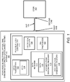
- Figure 1 illustrates an architectural layout of a high speed bidirectional OTDR-based testing apparatus (hereinafter also referred to as "apparatus 100") in accordance with an example of the present disclosure.
- the apparatus 100 may include a data transmitter 102 that is executed by at least one hardware processor (e.g., the hardware processor 902 of Figure 9 , and/or the hardware processor 1104 of Figure 11 ), to transmit data 104 from a first end of a device under test (DUT) 106 towards an OTDR 108 that is operatively connected to a second opposite end of the DUT 106.
- the apparatus 100 may also be an OTDR.
- the OTDR 108 may be another instantiation of the apparatus 100, and is designated apparatus 100' in Figure 5 .
- a data receiver 110 that is executed by at least one hardware processor (e.g., the hardware processor 902 of Figure 9 , and/or the hardware processor 1104 of Figure 11 ) may receive further data 112 that is transmitted by the OTDR 108 from the second opposite end of the DUT 106 towards the first end of the DUT 106.
- the hardware processor 902 of Figure 9 e.g., the hardware processor 902 of Figure 9 , and/or the hardware processor 1104 of Figure 11
- a signal quantization function that converts a data signal into a data bit stream may be performed by a dedicated hardware component such as a comparator or a function programmed in an field-programmable gate array (FPGA).
- a dedicated hardware component such as a comparator or a function programmed in an field-programmable gate array (FPGA).
- a receiver level controller 114 that is executed by at least one hardware processor (e.g., the hardware processor 902 of Figure 9 , and/or the hardware processor 1104 of Figure 11 ) may adjust, based on an amplitude of the further data 112, a direction of receiving of the further data 112 towards a first receiver that includes a low amplitude designated receiver 116 (e.g., see avalanche photodiode 514 and transimpedance amplifier 516 of Figure 5 ) of the data receiver 110 or towards a second receiver that includes a high amplitude designated receiver 118 (e.g., see tap PIN 554 photodiode and transimpedance PIN amplifier 556 of Figure 5 ) of the data receiver 110.
- a hardware processor e.g., the hardware processor 902 of Figure 9 , and/or the hardware processor 1104 of Figure 11
- the DUT 106 may include a fiber optic link.
- the apparatus 100 may further include a tap optical coupler 120 to extract part of optical power received from the OTDR 108 connected to the second opposite end of the DUT 106.
- the apparatus 100 may further include a tap PIN photodiode 122 operatively connected to the tap optical coupler 120 to convert an optical data stream, which corresponds to the further data 112, in the electric domain.
- the conversion of the optical data stream in the electric domain may be implemented to process an electrical signal for conversion into data.
- the apparatus 100 may include an optical attenuator to adjust a level of power of an optical source that transmits the data from the first end of the DUT towards the OTDR.
- the apparatus 100 may include an optical switch to switch, based on the received further data, between an input/output and a bidirectional optical sub-assemblies (BOSA)-based data receiver associated with the data receiver.
- BOSA bidirectional optical sub-assemblies
- the apparatus 100 may instead include an optical attenuator (e.g., see optical attenuator 600 of Figure 6 ) to adjust a level of power of an optical source that transmits the data from the first end of the DUT towards the OTDR.
- the apparatus 100 may include an avalanche photodiode (e.g., see avalanche photodiode 628 of Figure 6 ) to receive the further data that is transmitted by the OTDR from the second opposite end of the DUT towards the first end of the DUT.
- the apparatus 100 may include a transimpedance amplifier (e.g., see transimpedance amplifier 630 of Figure 6 ) operatively connected to the avalanche photodiode to receive the further data that is transmitted by the OTDR from the second opposite end of the DUT towards the first end of the DUT.
- a transimpedance amplifier e.g., see transimpedance amplifier 630 of Figure 6
- the apparatus 100 may include a laser current controller to adjust an output optical power of an optical source that is used to transmit the data.
- the laser current controller may utilize a laser driver and utilize a power control command to adjust the current of the laser driver.
- Figure 5 illustrates utilization of a photodiode coupled to a fiber optic link to illustrate operation of the apparatus 100, in accordance with an example of the present disclosure.
- the apparatus 100 may include a photodiode coupled to a device under test (DUT) 500, such as a fiber optic link, dedicated to receiving a data stream.
- a tap optical coupler 502 e.g., the tap optical coupler 120 of Figure 1
- the tap optical coupler 502 may be used for optical power monitoring.
- the tap optical coupler 502 may be associated with a PIN photodiode (junction composed of an intrinsic zone interposed between a heavily P-doped region and another heavily N-doped). The component integrating these two functions is then called PIN-TAP (or TAP PIN).
- the generator of an electrical test stimulus may control a laser driver 506 via a link 508.
- the laser driver 506 may in turn generate an electrical stimulus adapted to an optical source 510 (e.g., light source).
- a round-trip coupling device 512 may transmit the signal to the DUT 500 via the tap optical coupler 502.
- the signal returned by the DUT 500 may pass through the tap optical coupler 502, and then through the round-trip coupling device 512 to reach an avalanche photodiode (APD) 514.
- the photo-current from the avalanche photodiode 514 may then be directed to a transimpedance amplifier 516 connected to the reception stage of an OTDR receiver 518 via an electrical link 520.
- a second instantiation of the apparatus 100 may be connected to the other end of the DUT 500, and designated as apparatus 100' as shown in Figure 5 .
- the components for the apparatus 100' (which are identical to the components of the apparatus 100) are labeled differently from the components of the apparatus 100 to facilitate a description of the operation of the apparatus 100.
- the generator of an electrical test stimulus may control a laser driver 524 via a link 526.
- the laser driver 524 may in turn generate an electrical stimulus adapted to an optical source 528.
- a round-trip coupling device 530 may transmit the signal to the DUT 500 via a tap optical coupler 532.
- the signal returned by the DUT 500 may pass through the tap optical coupler 532, and then through the round-trip coupling device 530 to reach an avalanche photodiode 534.
- the photo-current from the avalanche photodiode 534 may then be directed to a transimpedance amplifier 536 connected to the reception stage of an OTDR receiver 538 via an electrical link 540.
- the laser driver 506 does not receive a signal from the PULSOR 504, but instead receives a signal from a transceiver 542 (e.g., the data transmitter 102 of Figure 1 ).
- the transceiver 542 may represent a software programmable hardware component that generates electrical data bit stream sent to the laser driver 506.
- Data may be sent on the DUT 500 through the round-trip coupling device 512 and the tap optical coupler 502. After transfer via the DUT 500, the data may be received on the avalanche photodiode 534 via the tap optical coupler 532 and the round-trip coupling device 530. The data may also be received on a tap PIN 544 photodiode via the tap optical coupler 532.
- the avalanche photodiode 534 channel may be reserved for the reception of low power signals, while the tap PIN 544 photodiode channel may be used to avoid reception saturation linked to high amplitude signals received from the DUT 500.
- an OTDR may emit optical power which may be approximately 0 dBm.
- the insertion loss between distant OTDRs may be up to 40 or 45 dB, and thus the optical power received by an OTDR may vary between 0 and - 45 dBm. Due to the wide variation of this received power, the avalanche photodiode 514 may not be usable for the entire power range.
- the tap PIN 554 photodiode may be utilized when input power is higher than -20 dBm, and for lower power, the avalanche photodiode 514 may be utilized.
- the avalanche photodiode 514 may represent a high sensitivity component for which output level is saturated when input power is too high, where the input power may be considered too high when data cannot be recovered after detection of this power by the avalanche photodiode 514.
- the tap PIN 554 photodiode may be utilized due to its higher optical power saturation level, which may represent a state when input power is higher than -20 dBm.
- a transimpedance PIN (TIA PIN) amplifier 548 may receive the photo-current from the tap PIN 544 photodiode.
- the output of the transimpedance PIN amplifier 548 may be connected to a data receiver reception stage 550 dedicated to the data signal.
- the symmetrical diagram and the data transfer operation may be identical for the reception chain avalanche photodiode 514, transimpedance amplifier 516, electrical link 520 and data receiver 552 (e.g., the high amplitude designated receiver 118 of Figure 1 ), as well as for the reception chain tap PIN 554 photodiode (e.g., the PIN photodiode 122 of Figure 1 ), transimpedance PIN amplifier 556, and data receiver 558 (e.g., the low amplitude designated receiver 116 of Figure 1 ).
- the data receiver 110 of Figure 1 may include the data receiver 552 and the data receiver 558.
- Optical data may be received by the avalanche photodiode 514 which converts the signal in electrical photocurrent.
- the transimpedance amplifier 516 may amplify and convert this current into a voltage signal. This signal may then be processed by the data receiver 552 to obtain data.
- the data receivers 552 and 558 may include a dedicated hardware component such as a quantizer or analog comparator which compares a signal with a threshold, and may further include a software programmable hardware component that is programmed to receive data.
- the laser driver 524 does not receive the signal from the PULSOR 522, but instead receives the signal from a transceiver 564. In the case of strong (e.g., high amplitude) signals received from the DUT 500, part of the signals may be picked up by the tap optical coupler 502 and sent to the tap PIN 554 photodiode via a link 562.
- the example of Figure 5 may utilize dedicated data receivers (e.g., 550, 558, 552 and 560), as well as dedicated data transmitters in order to optimize the performance with respect to digital data exchange between the OTDR instruments (e.g., the apparatus 100 and the apparatus 100') located on either side of the DUT 500.
- dedicated data receivers e.g., 550, 558, 552 and 560
- dedicated data transmitters e.g., a data transmitters located on either side of the DUT 500.
- Figure 6 illustrates a configuration based on attenuation of an emitted optical signal to illustrate operation of the apparatus 100, in accordance with an example of the present disclosure.
- the configuration of Figure 6 may represent the case of a multi-wavelength system (in this case two) in order to illustrate that the optical attenuator is not dedicated to a single source.
- an optical attenuator 600 may be inserted between a round-trip coupling device 602 (e.g., optical coupler) and a wavelength multiplexer 604 (MUX).
- MUX wavelength multiplexer
- the operation of the transmission and reception chains, which implement the pulsors (606 and 608), the data transmitters (610 and 612), the OTDR receiver 614 as well as the receivers dedicated to the exchanges of digital data remains identical to corresponding components of Figure 5 .
- use of the optical attenuator 600 provides for lowering of the optical power, avoiding saturation of avalanche photodiode 628 and removal of components 558, 556, 554 and 502 of Figure 5 .
- FIG. 6 To facilitate an understanding of Figure 6 , only one of the two apparatus (e.g., similar to apparatus 100 or apparatus 100') connected on either side of the DUT 640 is shown in Figure 6 . However, in a similar manner as Figure 5 , an apparatus 100 that includes all of the components of Figure 6 , and a second apparatus 100' may be connected to an opposite end of the DUT 640.
- the detection sensitivity may be adjusted by attenuating the signal emitted using the optical attenuator 600.
- the optical attenuator 600 may reduce the optical power emitted, and thereby the optical power received at the other end of the DUT 640. This operation may require prior communication between the OTDRs located on either side of the DUT 640 to communicate the saturation state of the avalanche photodiode reception chain. With respect to determination of saturation, in the presence of photocurrent received by transimpedance amplifier 630, the saturation may be detected as the signal crosses a predefined saturation level threshold or it is not possible to decode data.
- Saturation may represent a condition when input optical power is too high so that this variation of optical power is not converted linearly into variation of electrical output current.
- the configuration of Figure 6 may be implemented by utilizing hardware and software functions dedicated to data transmission on the DUT 640 and a sensitivity optimization system.
- the optimization may be based on reaching an optical power detected by avalanche photodiode 628 by adjusting the optical attenuator 600 of the remote OTDR on the other side of the DUT 640.
- the generator of an electrical test stimulus may control a laser driver 616 via a link 618.
- the laser driver 616 may in turn generate an electrical stimulus adapted to an optical source 620 (e.g., light source).
- the generator of an electrical test stimulus may control a laser driver 622 via a link 624.
- the laser driver 622 may in turn generate an electrical stimulus adapted to an optical source 626 (e.g., light source).
- the wavelength multiplexer 604 may represent a passive optical device that combines the optical signals from the optical source 620 and the optical source 626 according to their wavelengths.
- the photo-current from an avalanche photodiode 628 may be directed to a transimpedance amplifier 630 connected to the reception stage of the OTDR receiver 614 via an electrical link 632.
- the operation of data receiver 634 may be similar to that for data receiver 552 of Figure 5 .
- Figure 7 illustrates utilization of an optical switch to illustrate operation of the apparatus 100, in accordance with an example of the present disclosure.
- an optical switch 700 may be utilized to place the apparatus 100 in receiver mode on a dedicated channel using BOSA 702 (Bidirectional Optical Sub-Assemblies) technology.
- the BOSA 702 may combine the source 704, receiver 706 and optical coupler 708 devices.
- Management of the reception sensitivity may be performed by arbitrating the selection of the reception channel according to the sensitivity, either via the avalanche photodiode 710 or via the use of the optical switch 700, and the transmission reception system using the BOSA 702 and data receiver 712.
- the branch with the BOSA 702 may be used by default, but when input optical power on the BOSA 702 is too low so that a signal is not detected, a switch is made to the other branch and the optical power will be detected by avalanche photodiode 710 which has higher sensitivity.
- the combination of the BOSA 702 and data transmit and receive systems (respectively 714 and 712) may implement a transceiver function for data transmission.
- a round-trip coupling device 716 may transmit a signal to the DUT 718 via the optical switch 700.
- data may be sent on the DUT 718 through the round-trip coupling device 716 and the optical switch 700.
- the laser driver 730 does not receive a signal from the PULSOR, but instead receives a signal from a transceiver 720.
- the data transfer operation may be identical for the avalanche photodiode 710, transimpedance amplifier 722, electrical link 724, and data receiver 726.
- a data signal may be sent with the transceiver 720 and received by the avalanche photodiode 710 of the remote OTDR, and converted into data Rx.
- the transceiver 714 may send a data signal using source 704 of BOSA 702 of a first OTDR (e.g., apparatus 100 in a similar manner as in Figure 5 ), and a second remote OTDR (e.g., apparatus 100' in a similar manner as in Figure 5 ) may receive a signal by its receiver (e.g., PIN photodiode) that is similar to receiver 706, of its BOSA that is similar to BOSA 702.
- a first OTDR e.g., apparatus 100 in a similar manner as in Figure 5
- a second remote OTDR e.g., apparatus 100' in a similar manner as in Figure 5
- receiver e.g., PIN photodiode
- Figure 8 illustrates a further alternative configuration of the apparatus 100, in accordance with an example of the present disclosure.
- the configuration of Figure 8 may implement a laser driver 800 integrating the possibility of attenuating the laser current continuously or in steps.
- a laser current controller 802 may reduce the optical power of the optical source 804.
- the example of Figure 8 may combine the use of hardware (e.g., transceiver 806, data receiver 808, etc.), and software functions dedicated to data transmission on the DUT 810 and a receiver sensitivity optimization system controlling the level of power of the source.
- the laser current controller 802 may be used to reduce the optical power emitted, and thereby the optical power received at the other end of the DUT 810 by the distant OTDR. This operation may utilize prior communication between the OTDRs located on either side of the DUT 810 to communicate the saturation state of the avalanche photodiode reception chain.
- the optical power control of the source may need to use a source with a monitor photo diode or may need to add a PIN-TAP to measure the optical power sent to the line.
- Figures 9-11 respectively illustrate an example block diagram 900, a flowchart of an example method 1000, and a further example block diagram 1100 for high speed bidirectional OTDR-based testing, according to examples.
- the block diagram 900, the method 1000, and the block diagram 1100 may be implemented on the apparatus 00 described above with reference to Figure 1 by way of example and not of limitation.
- the block diagram 900, the method 1000, and the block diagram 1100 may be practiced in other apparatuses.
- Figure 9 shows hardware of the apparatus 00 that may execute the instructions of the block diagram 900.
- the hardware may include a processor 902, and a memory 904 storing machine readable instructions that when executed by the processor cause the processor to perform the instructions of the block diagram 900.
- the memory 904 may represent a non-transitory computer readable medium.
- Figure 10 may represent an example method for high speed bidirectional OTDR-based testing, and the steps of the method.
- Figure 11 may represent a non-transitory computer readable medium 1102 having stored thereon machine readable instructions to provide high speed bidirectional OTDR-based testing according to an example.
- the machine readable instructions when executed, cause a processor 1104 to perform the instructions of the block diagram 1100 also shown in Figure 11 .
- the processor 902 of Figure 9 and/or the processor 1104 of Figure 11 may include a single or multiple processors or other hardware processing circuit, to execute the methods, functions and other processes described herein. These methods, functions and other processes may be embodied as machine readable instructions stored on a computer readable medium, which may be non-transitory (e.g., the non-transitory computer readable medium 1102 of Figure 11 ), such as hardware storage devices (e.g., RAM (random access memory), ROM (read only memory), EPROM (erasable, programmable ROM), EEPROM (electrically erasable, programmable ROM), hard drives, and flash memory).
- the memory 904 may include a RAM, where the machine readable instructions and data for a processor may reside during runtime.
- the memory 904 may include instructions 906 to transmit data from a first end of a device under test (DUT) towards an optical time-domain reflectometer (OTDR) that is operatively connected to a second opposite end of the DUT.
- DUT device under test
- OTD optical time-domain reflectometer
- the processor 902 may fetch, decode, and execute the instructions 908 to receive further data that is transmitted by the OTDR from the second opposite end of the DUT towards the first end of the DUT.
- the processor 902 may fetch, decode, and execute the instructions 910 to adjust, based on an amplitude of the further data, a direction of receiving of the further data towards a first receiver of the data receiver or towards a second receiver of the data receiver.
- the method may include transmitting, by at least one hardware processor, data from a first end of a device under test (DUT) towards an optical time-domain reflectometer (OTDR) that is operatively connected to a second opposite end of the DUT.
- DUT device under test
- OTD optical time-domain reflectometer
- the method may include receiving, by the at least one hardware processor, further data that is transmitted by the OTDR from the second opposite end of the DUT towards the first end of the DUT.
- the method may include switching, by an optical switch 700, based on the received further data, between an input/output (e.g., round-trip coupling device 716) and a bidirectional optical sub-assemblies (BOSA)-based data receiver 702 associated with the data receiver.
- an input/output e.g., round-trip coupling device 716
- BOSA bidirectional optical sub-assemblies
- the method may include switching, by the optical switch, based on an optical power associated with the received further data, between the input/output and the BOSA-based data receiver associated with the data receiver.
- the method may include switching, by the optical switch, based on a relatively low optical power associated with the received further data, to the input/output data receiver that includes an avalanche photodiode.
- the method may include switching, by the optical switch, based on a relatively high optical power associated with the received further data, to the BOSA-based data receiver.
- the non-transitory computer readable medium 1102 may include instructions 1106 to transmit data from a first end of a device under test (DUT) towards an optical time-domain reflectometer (OTDR) that is operatively connected to a second opposite end of the DUT.
- DUT device under test
- OTD optical time-domain reflectometer
- the processor 1104 may fetch, decode, and execute the instructions 1108 to receive further data that is transmitted by the OTDR from the second opposite end of the DUT towards the first end of the DUT.
- the processor 1104 may fetch, decode, and execute the instructions 1110 to adjust, by a laser current controller (e.g., laser current controller 802), an output optical power of an optical source that is used to transmit the data.
- a laser current controller e.g., laser current controller 802
- the processor 1104 may fetch, decode, and execute the instructions to receive, by an avalanche photodiode (e.g., see "APD" of Figure 8 ), the further data that is transmitted by the OTDR from the second opposite end of the DUT towards the first end of the DUT.
- an avalanche photodiode e.g., see "APD” of Figure 8
- the processor 1104 may fetch, decode, and execute the instructions to receive, by a transimpedance amplifier (e.g., see “TIA APD” of Figure 8 ) operatively connected to the avalanche photodiode, the further data that is transmitted by the OTDR from the second opposite end of the DUT towards the first end of the DUT.
- a transimpedance amplifier e.g., see "TIA APD” of Figure 8
Abstract
Description
- A fiber optic cable may include one or more optical fibers that may be used to transmit light from a source to a destination. The optical fibers of the fiber optic cable may be referred to as fiber optic links. Fiber optic cables may represent a network element of a fiber optic network. In this regard, other types of network elements may include optical connectors, optical splices, optical couplers, and optical switches. A fiber optic network may be monitored, for example, by a remote fiber monitoring system that enables oversight of an entire fiber optic network from a central location. According to a first aspect of the present invention there is provided an apparatus comprising:
- a data transmitter, executed by at least one hardware processor, to
transmit data from a first end of a device under test (DUT) towards an optical time-domain reflectometer (OTDR) that is operatively connected to a second opposite end of the DUT; - a data receiver, executed by the at least one hardware processor, to
receive further data that is transmitted by the OTDR from the second opposite end of the DUT towards the first end of the DUT; and - a receiver level controller, executed by the at least one hardware processor, to
adjust, based on an amplitude of the further data, a direction of receiving of the further data towards a first receiver of the data receiver or towards a second receiver of the data receiver. The DUT may include a fiber optic link. The receiver level controller may include a tap optical coupler to extract part of optical power received from the OTDR connected to the second opposite end of the DUT. The apparatus may further comprise:
a tap PIN photodiode operatively connected to the tap optical coupler to convert an optical data stream, which corresponds to the further data, in an electric domain. The receiver level controller may be executed by the at least one hardware processor to adjust, based on the amplitude of the further data, the direction of receiving of the further data towards the first receiver of the data receiver or towards the second receiver of the data receiver by:
adjusting, based on the amplitude of the further data, the direction of receiving of the further data towards the first receiver that includes a low amplitude designated receiver or towards the second receiver that includes a high amplitude designated receiver. The receiver level controller may be executed by the at least one hardware processor to adjust, based on the amplitude of the further data, the direction of receiving of the further data towards the first receiver that includes the low amplitude designated receiver by:
adjusting, based on the amplitude of the further data, the direction of receiving of the further data towards the low amplitude designated receiver that includes an avalanche photodiode. The receiver level controller may be executed by the at least one hardware processor to adjust, based on the amplitude of the further data, the direction of receiving of the further data towards the first receiver that includes the low amplitude designated receiver by:
adjusting, based on the amplitude of the further data, the direction of receiving of the further data towards the low amplitude designated receiver that includes a transimpedance amplifier operatively connected to the avalanche photodiode. The receiver level controller may be executed by the at least one hardware processor to adjust, based on the amplitude of the further data, the direction of receiving of the further data towards the second receiver that includes the high amplitude designated receiver by:
adjusting, based on the amplitude of the further data, the direction of receiving of the further data towards the high amplitude designated receiver that includes a tap PIN photodiode. The receiver level controller may be executed by the at least one hardware processor to adjust, based on the amplitude of the further data, the direction of receiving of the further data towards the second receiver that includes the high amplitude designated receiver by:
adjusting, based on the amplitude of the further data, the direction of receiving of the further data towards the high amplitude designated receiver that includes a transimpedance PIN amplifier operatively connected to the tap PIN photodiode. According to further aspect of the present disclosure there is provided an apparatus comprising:- a data transmitter, executed by at least one hardware processor, to
transmit data from a first end of a device under test (DUT) towards an optical time-domain reflectometer (OTDR) that is operatively connected to a second opposite end of the DUT; - a data receiver, executed by the at least one hardware processor, to
receive further data that is transmitted by the OTDR from the second opposite end of the DUT towards the first end of the DUT; and - an optical attenuator to adjust a level of power of an optical source that transmits the data from the first end of the DUT towards the OTDR. The DUT may include a fiber optic link. The data receiver may comprise:
an avalanche photodiode to receive the further data that is transmitted by the OTDR from the second opposite end of the DUT towards the first end of the DUT. The data receiver may comprise:
a transimpedance amplifier operatively connected to the avalanche photodiode to receive the further data that is transmitted by the OTDR from the second opposite end of the DUT towards the first end of the DUT. According to a yet further aspect of the present disclosure there is provided a method comprising:- transmitting, by at least one hardware processor, data from a first end of a device under test (DUT) towards an optical time-domain reflectometer (OTDR) that is operatively connected to a second opposite end of the DUT;
- receiving, by the at least one hardware processor, further data that is transmitted by the OTDR from the second opposite end of the DUT towards the first end of the DUT; and
- switching, by an optical switch, based on the received further data, between an input/output data receiver and a bidirectional optical sub-assemblies (BOSA)-based data receiver associated with the data receiver. Switching, by the optical switch, based on the received further data, between the input/output data receiver and the BOSA-based data receiver associated with the data receiver, may further comprise:
switching, by the optical switch, based on an optical power associated with the received further data, between the input/output data receiver and the BOSA-based data receiver associated with the data receiver. Switching, by the optical switch, based on the received further data, between the input/output data receiver and the BOSA-based data receiver associated with the data receiver, may further comprise:
switching, by the optical switch, based on a relatively low optical power associated with the received further data, to the input/output data receiver that includes an avalanche photodiode. Switching, by the optical switch, based on the received further data, between the input/output data receiver and the BOSA-based data receiver associated with the data receiver, may further comprise:
switching, by the optical switch, based on a relatively high optical power associated with the received further data, to the BOSA-based data receiver. According to still further aspect of the present disclosure there is provided anontransitory computer readable medium having stored thereon machine readable instructions, the machine readable instructions, when executed by at least one hardware processor, cause the at least one hardware processor to:- transmit data from a first end of a device under test (DUT) towards an optical time-domain reflectometer (OTDR) that is operatively connected to a second opposite end of the DUT;
- receive further data that is transmitted by the OTDR from the second opposite end of the DUT towards the first end of the DUT; and
- adjust, by a laser current controller, an output optical power of an optical source that is used to transmit the data. The machine readable instructions, when executed by the at least one hardware processor, may cause the at least one hardware processor to:
receive, by an avalanche photodiode, the further data that is transmitted by the OTDR from the second opposite end of the DUT towards the first end of the DUT. The machine readable instructions, when executed by the at least one hardware processor, may cause the at least one hardware processor to:
receive, by a transimpedance amplifier operatively connected to the avalanche photodiode, the further data that is transmitted by the OTDR from the second opposite end of the DUT towards the first end of the DUT.
- a data transmitter, executed by at least one hardware processor, to
- Features of the present disclosure are illustrated by way of example and not limited in the following figure(s), in which like numerals indicate like elements, in which:
-
Figure 1 illustrates an architectural layout of a high speed bidirectional optical time-domain reflectometer (OTDR)-based testing apparatus in accordance with an example of the present disclosure; -
Figures 2A and 2B illustrate testing of a fiber optic link (e.g., a device under test (DUT)) in both directions by an OTDR, andFigure 2C illustrates automated bidirectional testing of the fiber optic link, in accordance with an example of the present disclosure; -
Figure 3A illustrates a principle of reducing insertion loss measurement errors related to a difference in Rayleigh backscattering coefficients between fiber optic links, andFigures 3B and3C respectively illustrate a combination of the curves or the measurement results of the measurements carried out in both directions, in accordance with an example of the present disclosure; -
Figure 4 illustrates half-sum of the insertion losses obtained on both sides to remove the influence of relative Rayleigh backscattering coefficients, in accordance with an example of the present disclosure; -
Figure 5 illustrates utilization of a photodiode coupled to a fiber optic link to illustrate operation of the high speed bidirectional OTDR-based testing apparatus ofFigure 1 , in accordance with an example of the present disclosure; -
Figure 6 illustrates a configuration based on attenuation of an emitted optical signal to illustrate operation of the high speed bidirectional OTDR-based testing apparatus ofFigure 1 , in accordance with an example of the present disclosure; -
Figure 7 illustrates utilization of an optical switch to illustrate operation of the high speed bidirectional OTDR-based testing apparatus ofFigure 1 , in accordance with an example of the present disclosure; -
Figure 8 illustrates a further alternative configuration of the high speed bidirectional OTDR-based testing apparatus ofFigure 1 , in accordance with an example of the present disclosure; -
Figure 9 illustrates an example block diagram for high speed bidirectional OTDR-based testing in accordance with an example of the present disclosure; -
Figure 10 illustrates a flowchart of an example method for high speed bidirectional OTDR-based testing in accordance with an example of the present disclosure; and -
Figure 11 illustrates a further example block diagram for high speed bidirectional OTDR-based testing in accordance with another example of the present disclosure. - For simplicity and illustrative purposes, the present disclosure is described by referring mainly to examples. In the following description, numerous specific details are set forth in order to provide a thorough understanding of the present disclosure. It will be readily apparent however, that the present disclosure may be practiced without limitation to these specific details. In other instances, some methods and structures have not been described in detail so as not to unnecessarily obscure the present disclosure.
- Throughout the present disclosure, the terms "a" and "an" are intended to denote at least one of a particular element. As used herein, the term "includes" means includes but not limited to, the term "including" means including but not limited to. The term "based on" means based at least in part on.
- High speed bidirectional Optical Time Domain Reflectometer (OTDR)-based testing apparatuses, methods for high speed bidirectional OTDR-based testing, and non-transitory computer readable media for high speed bidirectional OTDR-based testing are disclosed herein. The apparatuses, methods, and non-transitory computer readable media disclosed herein provide for relatively high test speeds, for example, for data transfers such as transfer of OTDR measurement point files, within a relatively short time duration. In this regard, the apparatuses, methods, and non-transitory computer readable media disclosed herein provide for high-performance communication based on the implementation of hardware and software functionality that is dedicated to the transfer of data.
- With respect to the apparatuses, methods, and non-transitory computer readable media disclosed herein, an OTDR may utilize Rayleigh backscattering and Fresnel reflection signals to monitor events with respect to a fiber optic network. One of the unique advantages of OTDR testing is that it utilizes access to one end of a fiber optic cable that may include a plurality of fiber optic links. Since distance and attenuation measurements are based on Rayleigh optical backscattering and the Fresnel reflection principle, returned light may be analyzed directly from the one end of a fiber optic link of the fiber optic cable.
- In order to minimize the impact of errors and uncertainties that can accompany one-way testing of a fiber optic link, two-way reflectometry test methods may be utilized to improve the precision and accuracy of testing of a fiber optic link. The two-way reflectometry test methods may be denoted as bidirectional reflectometry testing. For bidirectional reflectometry testing, a fiber optic link may be characterized by measuring attenuation and loss from both ends of the fiber optic link.
- For example,
Figures 2A and 2B illustrate testing of a fiber optic link (e.g., a device under test (DUT) as disclosed herein) in both directions by an OTDR, in accordance with an example of the present disclosure. - Referring to
Figure 2A , in order to perform bidirectional testing of afiber optic link 200, thefiber optic link 200 may be operatively connected to alaunch fiber 202 and a receivefiber 204 at opposite ends thereof. For example, thelaunch fiber 202 may be operatively connected to port of OTDR-1 at 206, and to a DUT that may include thefiber optic link 200. Thelaunch fiber 202 may be used to interface the OTDR-1 with thefiber optic link 200 in order to limit the risk of damage to the optical connector of the OTDR-1 by reducing the number of optical connections and disconnections. The launch and receive fibers may also provide for full characterization of the end connections of thefiber optic link 200. - The launch and receive fibers may create a symmetrical configuration at both ends of the
fiber optic link 200. In bidirectional OTDR testing, the samefiber optic link 200 may be tested in both directions using one or two OTDRs (e.g., OTDR-1 at 206 ofFigure 2A , and OTDR-2 at 208 ofFigure 2B ). The average of the results obtained in both directions may then be determined. - Compared to unidirectional testing of a fiber optic link, bidirectional fiber optic link testing may provide higher accuracy results with respect to characterization of the fiber optic link. Since Rayleigh backscatter is used to quantify the fiber optic link attenuation and insertion loss of each event, the fiber optic link backscatter coefficient may need to be known and programmed into the OTDR. This coefficient can vary between different fiber optic links, and the OTDR may display excessive attenuation or even negative attenuation (e.g., gain) at the junctions between fiber optic links with different coefficients. The actual value of the fiber optic link attenuation and of each event during the presence of fibers with different coefficients on the same fiber optic link may be determined by averaging the results obtained with a bidirectional OTDR test.
- If a fiber optic link with a lower backscatter coefficient has been soldered to a fiber optic link with a higher backscatter coefficient, the splice attenuation measured by the OTDR may be negative (e.g., therefore false). This effect may be designated as a "gain" because the amount of backscatter observed may be higher after the event than before. Conversely, if a fiber optic link with a higher backscatter coefficient has been soldered to a fiber optic link with a lower backscatter coefficient, the splice attenuation measured by the OTDR may be greater than the actual attenuation of that splice. By averaging the values obtained from the two ends of the fiber optic link, the actual value of the attenuation of a splice or connection may be obtained.
-
Figures 3A-3B illustrate a principle of reducing insertion loss measurement errors related to a difference in Rayleigh backscattering coefficients between fiber optic links, and a combination of the curves or the measurement results of the measurements carried out in both directions, in accordance with an example of the present disclosure. - Specifically,
Figure 3A shows the principle of reducing insertion loss measurement errors related to the difference in Rayleigh backscattering coefficients between fiber optic link-2 (e.g., Fiber-2), and fiber optic link-1 and fiber optic link-3 (e.g., Fiber-1 and Fiber 3). In this regard, Fiber-1, Fiber-2, and Fiber-3, may be respectively connected at Splice-A and Splice-B, with a 0.05 dB apparent loss/gain at the junctions of the splices.Figures 3B and3C respectively illustrate the combination of curves or measurement results of the measurements performed in both directions. In this regard,Figures 3B and3C provide for the apparent loss values to be obtained. In this regard, the half-sum of the insertion losses may be obtained on both sides of the fiber optic link to remove the influence of the relative Rayleigh backscattering coefficients. -
Figure 4 illustrates half-sum of the insertion losses obtained on both sides for the fiber optic links ofFigures 3A-3C to remove the influence of the relative Rayleigh backscattering coefficients, in accordance with an example of the present disclosure. For example,Figure 4 provides examples of half-sum determination, where the values 0-> E and E->0 may be added and then divided by two. - In some bidirectional reflectometry techniques, such as the technique of
Figures 2A and 2B , an OTDR, such as OTDR-1 may be connected to one end of a fiber optic link to perform a measurement in one direction, and the same OTDR may be disconnected and connected to an opposite end of the fiber optic link to perform a second measurement in an opposite direction. In other bidirectional reflectometry techniques as illustrated inFigure 2C , which may be referred to as automated bidirectional reflectometry techniques, by pairing a local OTDR with a far end OTDR connected at the opposite end of the fiber optic link (e.g., or a fiber optic cable including the fiber optic link), communication between the two OTDRs will ensure identical test configurations, continuity of the fiber link, and easier acquisition and compilation of data. In this regard, the measurement time may also be reduced while ensuring the quality of the measurements and reducing the risk of errors. The automated functionality may be used to perform reflectometry tests at multiple wavelengths (e.g., to improve detection of fiber optic link bends), and include bidirectional attenuation and optical reflection loss (ORL) tests. - In other bidirectional OTDR reflectometry techniques, such as a "loop back" testing technique, rather than utilizing a second OTDR at the far end of the fiber optic link, a loopback cable may connect one fiber optic link to another fiber optic link which is also to be tested. In this way, an OTDR test pulse may be sent down one fiber optic link and continues through the loop back and down the second fiber optic link, thus testing both fibers uni-directionally at the same time. To gain the benefit of bidirectional OTDR testing, both fiber optic links (including the loop back) may then be tested in the opposite direction from the same location. This technique may use an OTDR approach such as where a single OTDR is moved from the first to the second fiber optic link to manually test in each direction and the results may be manually combined, or an automated OTDR approach where two OTDRs are used, one connected to each fiber optic link end to automatically test each direction and combine test results.
- With respect to automated bidirectional testing of a fiber optic link, multipurpose OTDRs and testers may be configured for automated bidirectional reflectometry or other bidirectional fiber optic testing, at the push of a button. These devices may also include a built-in feature that allows them to generate reports for speed and convenience. For example, when making an automated bidirectional measurement on a fiber optic link, the test instruments (e.g., OTDRs) may need to exchange data to synchronize the measurement, exchange setup information, and exchange results. For example, as disclosed in commonly owned
U.S. Patent Application No. 16/152,046 , titled "OPTICAL TIME-DOMAIN REFLECTOMETER DEVICE INCLUDING MULTIPLE AND BI-DIRECTIONAL OPTICAL TESTING FOR FIBER ANALYSIS", the disclosure of which is incorporated by reference in its entirety, the OTDR devices may implement frequency modulation to exchange data. Each synchronization, events and measurement results may be encoded by a frequency. However, this process of sending and decoding data may include a plurality of sequences of data exchange. In this regard, it is technically challenging to further reduce a time needed to exchange data between two or more test instruments (e.g., OTDRs). - The apparatuses, methods, and non-transitory computer readable media disclosed herein address the aforementioned technical challenges by providing for relatively high test speeds, for example, for data transfers such as transfer of OTDR measurement point files, within a relatively short time duration. In this regard, the apparatuses, methods, and non-transitory computer readable media disclosed herein provide for high-performance communication based on the implementation of hardware and software functionality that is dedicated to the transfer of data. For example, the apparatuses, methods, and non-transitory computer readable media disclosed herein provide for utilization of an OTDR and the DUT (e.g., a fiber optic link) to exchange data without using another communication device, such as Ethernet, WiFi, Global System for Mobiles (GSM), or an optical transceiver using fibers other than the DUT. Thus, the apparatuses, methods, and non-transitory computer readable media disclosed herein provide for utilization of an OTDR and the DUT to exchange data, such as OTDR trace data, at relatively high speeds. The apparatuses, methods, and non-transitory computer readable media disclosed herein also provide for communication establishment to test the continuity of a fiber optic link.
- For the apparatus, methods, and non-transitory computer readable media disclosed herein, the elements of the apparatus, methods, and non-transitory computer readable media disclosed herein may be any combination of hardware and programming to implement the functionalities of the respective elements. In some examples described herein, the combinations of hardware and programming may be implemented in a number of different ways. For example, the programming for the elements may be processor executable instructions stored on a non-transitory machine-readable storage medium and the hardware for the elements may include a processing resource to execute those instructions. In these examples, a computing device implementing such elements may include the machine-readable storage medium storing the instructions and the processing resource to execute the instructions, or the machine-readable storage medium may be separately stored and accessible by the computing device and the processing resource. In some examples, some elements may be implemented in circuitry.
-
Figure 1 illustrates an architectural layout of a high speed bidirectional OTDR-based testing apparatus (hereinafter also referred to as "apparatus 100") in accordance with an example of the present disclosure. - Referring to
Figure 1 , theapparatus 100 may include adata transmitter 102 that is executed by at least one hardware processor (e.g., thehardware processor 902 ofFigure 9 , and/or thehardware processor 1104 ofFigure 11 ), to transmitdata 104 from a first end of a device under test (DUT) 106 towards anOTDR 108 that is operatively connected to a second opposite end of theDUT 106. As disclosed herein in further detail with reference toFigure 5 , theapparatus 100 may also be an OTDR. Further, theOTDR 108 may be another instantiation of theapparatus 100, and is designated apparatus 100' inFigure 5 . - A
data receiver 110 that is executed by at least one hardware processor (e.g., thehardware processor 902 ofFigure 9 , and/or thehardware processor 1104 ofFigure 11 ) may receivefurther data 112 that is transmitted by theOTDR 108 from the second opposite end of theDUT 106 towards the first end of theDUT 106. - According to examples disclosed herein, for the
data receiver 110, a signal quantization function that converts a data signal into a data bit stream may be performed by a dedicated hardware component such as a comparator or a function programmed in an field-programmable gate array (FPGA). - As disclosed herein in further detail with reference to
Figure 5 , areceiver level controller 114 that is executed by at least one hardware processor (e.g., thehardware processor 902 ofFigure 9 , and/or thehardware processor 1104 ofFigure 11 ) may adjust, based on an amplitude of thefurther data 112, a direction of receiving of thefurther data 112 towards a first receiver that includes a low amplitude designated receiver 116 (e.g., seeavalanche photodiode 514 andtransimpedance amplifier 516 ofFigure 5 ) of thedata receiver 110 or towards a second receiver that includes a high amplitude designated receiver 118 (e.g., seetap PIN 554 photodiode andtransimpedance PIN amplifier 556 ofFigure 5 ) of thedata receiver 110. - According to examples disclosed herein, the
DUT 106 may include a fiber optic link. - According to examples disclosed herein, as disclosed herein in further detail with reference to
Figure 5 , theapparatus 100 may further include a tapoptical coupler 120 to extract part of optical power received from theOTDR 108 connected to the second opposite end of theDUT 106. - According to examples disclosed herein, as disclosed herein in further detail with reference to
Figure 5 , theapparatus 100 may further include atap PIN photodiode 122 operatively connected to the tapoptical coupler 120 to convert an optical data stream, which corresponds to thefurther data 112, in the electric domain. The conversion of the optical data stream in the electric domain may be implemented to process an electrical signal for conversion into data. - According to examples disclosed herein with respect to
Figures 5 and6 , instead of the tapoptical coupler 120 and thePIN photodiode 122 ofFigure 5 , as shown inFigure 6 , theapparatus 100 may include an optical attenuator to adjust a level of power of an optical source that transmits the data from the first end of the DUT towards the OTDR. - According to examples disclosed herein with respect to
Figures 1 ,5 , and7 , instead of the tapoptical coupler 120 and thePIN photodiode 122 ofFigure 5 , as shown inFigure 7 , theapparatus 100 may include an optical switch to switch, based on the received further data, between an input/output and a bidirectional optical sub-assemblies (BOSA)-based data receiver associated with the data receiver. - According to examples disclosed herein with respect to
Figures 1 ,5 , and6 , theapparatus 100 may instead include an optical attenuator (e.g., seeoptical attenuator 600 ofFigure 6 ) to adjust a level of power of an optical source that transmits the data from the first end of the DUT towards the OTDR. In this regard, theapparatus 100 may include an avalanche photodiode (e.g., seeavalanche photodiode 628 ofFigure 6 ) to receive the further data that is transmitted by the OTDR from the second opposite end of the DUT towards the first end of the DUT. Further, theapparatus 100 may include a transimpedance amplifier (e.g., seetransimpedance amplifier 630 ofFigure 6 ) operatively connected to the avalanche photodiode to receive the further data that is transmitted by the OTDR from the second opposite end of the DUT towards the first end of the DUT. - According to examples disclosed herein with respect to
Figures 5 and8 , instead of the tapoptical coupler 120 and thePIN photodiode 122 ofFigure 5 , as shown inFigure 8 , theapparatus 100 may include a laser current controller to adjust an output optical power of an optical source that is used to transmit the data. The laser current controller may utilize a laser driver and utilize a power control command to adjust the current of the laser driver. - Operation of the
apparatus 100 is described in further detail with reference toFigures 5-8 . -
Figure 5 illustrates utilization of a photodiode coupled to a fiber optic link to illustrate operation of theapparatus 100, in accordance with an example of the present disclosure. - Referring to
Figure 5 , theapparatus 100 may include a photodiode coupled to a device under test (DUT) 500, such as a fiber optic link, dedicated to receiving a data stream. A tap optical coupler 502 (e.g., the tapoptical coupler 120 ofFigure 1 ) may take part of the power from the line in which it is inserted. The tap optical coupler 502 may be used for optical power monitoring. Further, the tap optical coupler 502 may be associated with a PIN photodiode (junction composed of an intrinsic zone interposed between a heavily P-doped region and another heavily N-doped). The component integrating these two functions is then called PIN-TAP (or TAP PIN). - In an OTDR mode, the generator of an electrical test stimulus (e.g.,
PULSOR 504, which may represent an electrical pulse generator) may control alaser driver 506 via alink 508. Thelaser driver 506 may in turn generate an electrical stimulus adapted to an optical source 510 (e.g., light source). A round-trip coupling device 512 may transmit the signal to theDUT 500 via the tap optical coupler 502. - Still in the OTDR mode, the signal returned by the DUT 500 (Rayleigh backscatter and Fresnel reflection) may pass through the tap optical coupler 502, and then through the round-
trip coupling device 512 to reach an avalanche photodiode (APD) 514. The photo-current from theavalanche photodiode 514 may then be directed to atransimpedance amplifier 516 connected to the reception stage of an OTDR receiver 518 via anelectrical link 520. - A second instantiation of the
apparatus 100 may be connected to the other end of theDUT 500, and designated as apparatus 100' as shown inFigure 5 . However, the components for the apparatus 100' (which are identical to the components of the apparatus 100) are labeled differently from the components of theapparatus 100 to facilitate a description of the operation of theapparatus 100. - For the apparatus 100', the generator of an electrical test stimulus (e.g., PULSOR 522) may control a
laser driver 524 via alink 526. Thelaser driver 524 may in turn generate an electrical stimulus adapted to anoptical source 528. A round-trip coupling device 530 may transmit the signal to theDUT 500 via a tapoptical coupler 532. - Still in the OTDR mode, the signal returned by the DUT 500 (Rayleigh backscatter and Fresnel reflection) may pass through the tap
optical coupler 532, and then through the round-trip coupling device 530 to reach anavalanche photodiode 534. The photo-current from theavalanche photodiode 534 may then be directed to atransimpedance amplifier 536 connected to the reception stage of anOTDR receiver 538 via anelectrical link 540. - In the data transfer mode, the
laser driver 506 does not receive a signal from thePULSOR 504, but instead receives a signal from a transceiver 542 (e.g., thedata transmitter 102 ofFigure 1 ). Thetransceiver 542 may represent a software programmable hardware component that generates electrical data bit stream sent to thelaser driver 506. Data may be sent on theDUT 500 through the round-trip coupling device 512 and the tap optical coupler 502. After transfer via theDUT 500, the data may be received on theavalanche photodiode 534 via the tapoptical coupler 532 and the round-trip coupling device 530. The data may also be received on atap PIN 544 photodiode via the tapoptical coupler 532. Due to its sensitivity, theavalanche photodiode 534 channel may be reserved for the reception of low power signals, while thetap PIN 544 photodiode channel may be used to avoid reception saturation linked to high amplitude signals received from theDUT 500. With respect to a low power signal versus a high amplitude signal, an OTDR may emit optical power which may be approximately 0 dBm. The insertion loss between distant OTDRs may be up to 40 or 45 dB, and thus the optical power received by an OTDR may vary between 0 and - 45 dBm. Due to the wide variation of this received power, theavalanche photodiode 514 may not be usable for the entire power range. In this regard, thetap PIN 554 photodiode may be utilized when input power is higher than -20 dBm, and for lower power, theavalanche photodiode 514 may be utilized. In this regard, theavalanche photodiode 514 may represent a high sensitivity component for which output level is saturated when input power is too high, where the input power may be considered too high when data cannot be recovered after detection of this power by theavalanche photodiode 514. In such a case, thetap PIN 554 photodiode may be utilized due to its higher optical power saturation level, which may represent a state when input power is higher than -20 dBm. - In the case of strong (e.g., high amplitude) signals received from the
DUT 500, part of the signals may be picked up by the tapoptical coupler 532 and sent to thetap PIN 544 photodiode via alink 546. A transimpedance PIN (TIA PIN)amplifier 548 may receive the photo-current from thetap PIN 544 photodiode. The output of thetransimpedance PIN amplifier 548 may be connected to a data receiver reception stage 550 dedicated to the data signal. - The symmetrical diagram and the data transfer operation (e.g., from apparatus 100' to apparatus 100) may be identical for the reception
chain avalanche photodiode 514,transimpedance amplifier 516,electrical link 520 and data receiver 552 (e.g., the high amplitude designatedreceiver 118 ofFigure 1 ), as well as for the receptionchain tap PIN 554 photodiode (e.g., thePIN photodiode 122 ofFigure 1 ),transimpedance PIN amplifier 556, and data receiver 558 (e.g., the low amplitude designatedreceiver 116 ofFigure 1 ). For the example ofFigure 5 , thedata receiver 110 ofFigure 1 may include thedata receiver 552 and thedata receiver 558. Optical data may be received by theavalanche photodiode 514 which converts the signal in electrical photocurrent. Thetransimpedance amplifier 516 may amplify and convert this current into a voltage signal. This signal may then be processed by thedata receiver 552 to obtain data. Thedata receivers laser driver 524 does not receive the signal from thePULSOR 522, but instead receives the signal from atransceiver 564. In the case of strong (e.g., high amplitude) signals received from theDUT 500, part of the signals may be picked up by the tap optical coupler 502 and sent to thetap PIN 554 photodiode via alink 562. - The example of
Figure 5 may utilize dedicated data receivers (e.g., 550, 558, 552 and 560), as well as dedicated data transmitters in order to optimize the performance with respect to digital data exchange between the OTDR instruments (e.g., theapparatus 100 and the apparatus 100') located on either side of theDUT 500. -
Figure 6 illustrates a configuration based on attenuation of an emitted optical signal to illustrate operation of theapparatus 100, in accordance with an example of the present disclosure. - The configuration of
Figure 6 may represent the case of a multi-wavelength system (in this case two) in order to illustrate that the optical attenuator is not dedicated to a single source. Thus, anoptical attenuator 600 may be inserted between a round-trip coupling device 602 (e.g., optical coupler) and a wavelength multiplexer 604 (MUX). The operation of the transmission and reception chains, which implement the pulsors (606 and 608), the data transmitters (610 and 612), theOTDR receiver 614 as well as the receivers dedicated to the exchanges of digital data remains identical to corresponding components ofFigure 5 . Further, compared to the example ofFigure 5 , use of theoptical attenuator 600 provides for lowering of the optical power, avoiding saturation ofavalanche photodiode 628 and removal ofcomponents Figure 5 . - To facilitate an understanding of
Figure 6 , only one of the two apparatus (e.g., similar toapparatus 100 or apparatus 100') connected on either side of theDUT 640 is shown inFigure 6 . However, in a similar manner asFigure 5 , anapparatus 100 that includes all of the components ofFigure 6 , and a second apparatus 100' may be connected to an opposite end of theDUT 640. The detection sensitivity may be adjusted by attenuating the signal emitted using theoptical attenuator 600. When the reception chain and in particular theavalanche photodiode 534 of the remote OTDR (e.g., similar to the apparatus 100' (not shown) on the other side of the DUT 640) risks being saturated, theoptical attenuator 600 may reduce the optical power emitted, and thereby the optical power received at the other end of theDUT 640. This operation may require prior communication between the OTDRs located on either side of theDUT 640 to communicate the saturation state of the avalanche photodiode reception chain. With respect to determination of saturation, in the presence of photocurrent received bytransimpedance amplifier 630, the saturation may be detected as the signal crosses a predefined saturation level threshold or it is not possible to decode data. Saturation may represent a condition when input optical power is too high so that this variation of optical power is not converted linearly into variation of electrical output current. Thus, by managing the level of optical power, the configuration ofFigure 6 may be implemented by utilizing hardware and software functions dedicated to data transmission on theDUT 640 and a sensitivity optimization system. With respect to sensitivity optimization, the optimization may be based on reaching an optical power detected byavalanche photodiode 628 by adjusting theoptical attenuator 600 of the remote OTDR on the other side of theDUT 640. - With continued reference to
Figure 6 , in a similar manner as the configuration ofFigure 5 , in an OTDR mode, the generator of an electrical test stimulus (e.g., PULSOR 606) may control alaser driver 616 via alink 618. Thelaser driver 616 may in turn generate an electrical stimulus adapted to an optical source 620 (e.g., light source). - Similarly, the generator of an electrical test stimulus (e.g., PULSOR 608) may control a
laser driver 622 via alink 624. Thelaser driver 622 may in turn generate an electrical stimulus adapted to an optical source 626 (e.g., light source). Thewavelength multiplexer 604 may represent a passive optical device that combines the optical signals from theoptical source 620 and theoptical source 626 according to their wavelengths. - Still in the OTDR mode, the photo-current from an
avalanche photodiode 628 may be directed to atransimpedance amplifier 630 connected to the reception stage of theOTDR receiver 614 via anelectrical link 632. Further, the operation ofdata receiver 634 may be similar to that fordata receiver 552 ofFigure 5 . -
Figure 7 illustrates utilization of an optical switch to illustrate operation of theapparatus 100, in accordance with an example of the present disclosure. - Referring to
Figure 7 , compared to the configuration ofFigure 5 , anoptical switch 700 may be utilized to place theapparatus 100 in receiver mode on a dedicated channel using BOSA 702 (Bidirectional Optical Sub-Assemblies) technology. TheBOSA 702 may combine thesource 704,receiver 706 andoptical coupler 708 devices. - Management of the reception sensitivity may be performed by arbitrating the selection of the reception channel according to the sensitivity, either via the
avalanche photodiode 710 or via the use of theoptical switch 700, and the transmission reception system using theBOSA 702 anddata receiver 712. With respect to management of reception sensitivity, the branch with theBOSA 702 may be used by default, but when input optical power on theBOSA 702 is too low so that a signal is not detected, a switch is made to the other branch and the optical power will be detected byavalanche photodiode 710 which has higher sensitivity. The combination of theBOSA 702 and data transmit and receive systems (respectively 714 and 712) may implement a transceiver function for data transmission. - In a similar manner as disclosed herein with respect to
Figure 5 , in an OTDR mode, a round-trip coupling device 716 may transmit a signal to theDUT 718 via theoptical switch 700. In the data transfer mode, data may be sent on theDUT 718 through the round-trip coupling device 716 and theoptical switch 700. In the data transfer mode, thelaser driver 730 does not receive a signal from the PULSOR, but instead receives a signal from atransceiver 720. Further, as disclosed herein with respect toFigure 5 , the data transfer operation may be identical for theavalanche photodiode 710,transimpedance amplifier 722,electrical link 724, anddata receiver 726. - With reference to
Figures 5 and7 , for the OTDR and the data transfer modes forFigure 7 , in a first mode that is similar toFigure 5 , a data signal may be sent with thetransceiver 720 and received by theavalanche photodiode 710 of the remote OTDR, and converted into data Rx. In a second mode that uses theBOSA 702, thetransceiver 714 may send a datasignal using source 704 ofBOSA 702 of a first OTDR (e.g.,apparatus 100 in a similar manner as inFigure 5 ), and a second remote OTDR (e.g., apparatus 100' in a similar manner as inFigure 5 ) may receive a signal by its receiver (e.g., PIN photodiode) that is similar toreceiver 706, of its BOSA that is similar toBOSA 702. -
Figure 8 illustrates a further alternative configuration of theapparatus 100, in accordance with an example of the present disclosure. - Compared to the configuration of
Figure 5 , the configuration ofFigure 8 may implement alaser driver 800 integrating the possibility of attenuating the laser current continuously or in steps. In this regard, a lasercurrent controller 802 may reduce the optical power of theoptical source 804. As with the examples ofFigures 5-7 , the example ofFigure 8 may combine the use of hardware (e.g.,transceiver 806,data receiver 808, etc.), and software functions dedicated to data transmission on theDUT 810 and a receiver sensitivity optimization system controlling the level of power of the source. When the reception chain and in particular the avalanche photodiode of the remote OTDR risks being saturated, the lasercurrent controller 802 may be used to reduce the optical power emitted, and thereby the optical power received at the other end of theDUT 810 by the distant OTDR. This operation may utilize prior communication between the OTDRs located on either side of theDUT 810 to communicate the saturation state of the avalanche photodiode reception chain. The optical power control of the source may need to use a source with a monitor photo diode or may need to add a PIN-TAP to measure the optical power sent to the line. -
Figures 9-11 respectively illustrate an example block diagram 900, a flowchart of anexample method 1000, and a further example block diagram 1100 for high speed bidirectional OTDR-based testing, according to examples. The block diagram 900, themethod 1000, and the block diagram 1100 may be implemented on the apparatus 00 described above with reference toFigure 1 by way of example and not of limitation. The block diagram 900, themethod 1000, and the block diagram 1100 may be practiced in other apparatuses. In addition to showing the block diagram 900,Figure 9 shows hardware of the apparatus 00 that may execute the instructions of the block diagram 900. The hardware may include aprocessor 902, and amemory 904 storing machine readable instructions that when executed by the processor cause the processor to perform the instructions of the block diagram 900. Thememory 904 may represent a non-transitory computer readable medium.Figure 10 may represent an example method for high speed bidirectional OTDR-based testing, and the steps of the method.Figure 11 may represent a non-transitory computer readable medium 1102 having stored thereon machine readable instructions to provide high speed bidirectional OTDR-based testing according to an example. The machine readable instructions, when executed, cause aprocessor 1104 to perform the instructions of the block diagram 1100 also shown inFigure 11 . - The
processor 902 ofFigure 9 and/or theprocessor 1104 ofFigure 11 may include a single or multiple processors or other hardware processing circuit, to execute the methods, functions and other processes described herein. These methods, functions and other processes may be embodied as machine readable instructions stored on a computer readable medium, which may be non-transitory (e.g., the non-transitory computerreadable medium 1102 ofFigure 11 ), such as hardware storage devices (e.g., RAM (random access memory), ROM (read only memory), EPROM (erasable, programmable ROM), EEPROM (electrically erasable, programmable ROM), hard drives, and flash memory). Thememory 904 may include a RAM, where the machine readable instructions and data for a processor may reside during runtime. - Referring to
Figures 1-9 , and particularly toFigure 5 and the block diagram 900 shown inFigure 9 , thememory 904 may includeinstructions 906 to transmit data from a first end of a device under test (DUT) towards an optical time-domain reflectometer (OTDR) that is operatively connected to a second opposite end of the DUT. - The
processor 902 may fetch, decode, and execute theinstructions 908 to receive further data that is transmitted by the OTDR from the second opposite end of the DUT towards the first end of the DUT. - The
processor 902 may fetch, decode, and execute theinstructions 910 to adjust, based on an amplitude of the further data, a direction of receiving of the further data towards a first receiver of the data receiver or towards a second receiver of the data receiver. - Referring to
Figures 1-8 and10 , and particularlyFigures 7 and10 , for themethod 1000, atblock 1002, the method may include transmitting, by at least one hardware processor, data from a first end of a device under test (DUT) towards an optical time-domain reflectometer (OTDR) that is operatively connected to a second opposite end of the DUT. - At
block 1004, the method may include receiving, by the at least one hardware processor, further data that is transmitted by the OTDR from the second opposite end of the DUT towards the first end of the DUT. - At
block 1006, the method may include switching, by anoptical switch 700, based on the received further data, between an input/output (e.g., round-trip coupling device 716) and a bidirectional optical sub-assemblies (BOSA)-baseddata receiver 702 associated with the data receiver. - According to examples disclosed herein, the method may include switching, by the optical switch, based on an optical power associated with the received further data, between the input/output and the BOSA-based data receiver associated with the data receiver.
- According to examples disclosed herein, the method may include switching, by the optical switch, based on a relatively low optical power associated with the received further data, to the input/output data receiver that includes an avalanche photodiode.
- According to examples disclosed herein, the method may include switching, by the optical switch, based on a relatively high optical power associated with the received further data, to the BOSA-based data receiver.
- Referring to
Figures 1-8 and11 , and particularlyFigures 8 and11 , for the block diagram 1100, the non-transitory computer readable medium 1102 may includeinstructions 1106 to transmit data from a first end of a device under test (DUT) towards an optical time-domain reflectometer (OTDR) that is operatively connected to a second opposite end of the DUT. - The
processor 1104 may fetch, decode, and execute theinstructions 1108 to receive further data that is transmitted by the OTDR from the second opposite end of the DUT towards the first end of the DUT. - The
processor 1104 may fetch, decode, and execute theinstructions 1110 to adjust, by a laser current controller (e.g., laser current controller 802), an output optical power of an optical source that is used to transmit the data. - According to examples disclosed herein, the
processor 1104 may fetch, decode, and execute the instructions to receive, by an avalanche photodiode (e.g., see "APD" ofFigure 8 ), the further data that is transmitted by the OTDR from the second opposite end of the DUT towards the first end of the DUT. - According to examples disclosed herein, the
processor 1104 may fetch, decode, and execute the instructions to receive, by a transimpedance amplifier (e.g., see "TIA APD" ofFigure 8 ) operatively connected to the avalanche photodiode, the further data that is transmitted by the OTDR from the second opposite end of the DUT towards the first end of the DUT. - What has been described and illustrated herein is an example along with some of its variations. The terms, descriptions and figures used herein are set forth by way of illustration only and are not meant as limitations. Many variations are possible within the spirit and scope of the subject matter, which is intended to be defined by the following claims -- and their equivalents -- in which all terms are meant in their broadest reasonable sense unless otherwise indicated.
Claims (15)
- An apparatus comprising:a data transmitter, executed by at least one hardware processor, to
transmit data from a first end of a device under test (DUT) towards an optical time-domain reflectometer (OTDR) that is operatively connected to a second opposite end of the DUT;a data receiver, executed by the at least one hardware processor, to
receive further data that is transmitted by the OTDR from the second opposite end of the DUT towards the first end of the DUT; anda receiver level controller, executed by the at least one hardware processor, to
adjust, based on an amplitude of the further data, a direction of receiving of the further data towards a first receiver of the data receiver or towards a second receiver of the data receiver. - The apparatus according to claim 1, wherein the receiver level controller includes a tap optical coupler to extract part of optical power received from the OTDR connected to the second opposite end of the DUT and optionally further includes a tap PIN photodiode operatively connected to the tap optical coupler to convert an optical data stream, which corresponds to the further data, in an electric domain.
- The apparatus according to claim 1, wherein the receiver level controller is executed by the at least one hardware processor to adjust, based on the amplitude of the further data, the direction of receiving of the further data towards the first receiver of the data receiver or towards the second receiver of the data receiver by:
adjusting, based on the amplitude of the further data, the direction of receiving of the further data towards the first receiver that includes a low amplitude designated receiver or towards the second receiver that includes a high amplitude designated receiver. - The apparatus according to claim 3, wherein the receiver level controller is executed by the at least one hardware processor to adjust, based on the amplitude of the further data, the direction of receiving of the further data towards the first receiver that includes the low amplitude designated receiver by:
adjusting, based on the amplitude of the further data, the direction of receiving of the further data towards the low amplitude designated receiver that includes an avalanche photodiode. - The apparatus according to claim 4, wherein the receiver level controller is executed by the at least one hardware processor to adjust, based on the amplitude of the further data, the direction of receiving of the further data towards the first receiver that includes the low amplitude designated receiver by:
adjusting, based on the amplitude of the further data, the direction of receiving of the further data towards the low amplitude designated receiver that includes a transimpedance amplifier operatively connected to the avalanche photodiode. - The apparatus according to claim 3, wherein the receiver level controller is executed by the at least one hardware processor to adjust, based on the amplitude of the further data, the direction of receiving of the further data towards the second receiver that includes the high amplitude designated receiver by:
adjusting, based on the amplitude of the further data, the direction of receiving of the further data towards the high amplitude designated receiver that includes a tap PIN photodiode and optionally further includes a transimpedance PIN amplifier operatively connected to the tap PIN photodiode. - An apparatus comprising:a data transmitter, executed by at least one hardware processor, to
transmit data from a first end of a device under test (DUT) towards an optical time-domain reflectometer (OTDR) that is operatively connected to a second opposite end of the DUT;a data receiver, executed by the at least one hardware processor, to
receive further data that is transmitted by the OTDR from the second opposite end of the DUT towards the first end of the DUT; andan optical attenuator to adjust a level of power of an optical source that transmits the data from the first end of the DUT towards the OTDR. - The apparatus according to claim 7, wherein the data receiver comprises:
an avalanche photodiode to receive the further data that is transmitted by the OTDR from the second opposite end of the DUT towards the first end of the DUT and optionally further includes a transimpedance amplifier operatively connected to the avalanche photodiode to receive the further data that is transmitted by the OTDR from the second opposite end of the DUT towards the first end of the DUT. - A method comprising:transmitting, by at least one hardware processor, data from a first end of a device under test (DUT) towards an optical time-domain reflectometer (OTDR) that is operatively connected to a second opposite end of the DUT;receiving, by the at least one hardware processor, further data that is transmitted by the OTDR from the second opposite end of the DUT towards the first end of the DUT; andswitching, by an optical switch, based on the received further data, between an input/output data receiver and a bidirectional optical sub-assemblies (BOSA)-based data receiver associated with the data receiver.
- The method according to claim 10, wherein switching, by the optical switch, based on the received further data, between the input/output data receiver and the BOSA-based data receiver associated with the data receiver, further comprises:
switching, by the optical switch, based on an optical power associated with the received further data, between the input/output data receiver and the BOSA-based data receiver associated with the data receiver or switching, by the optical switch, based on a relatively low optical power associated with the received further data, to the input/output data receiver that includes an avalanche photodiode. - The method according to claim 11, wherein switching, by the optical switch, based on the received further data, between the input/output data receiver and the BOSA-based data receiver associated with the data receiver, further comprises:
switching, by the optical switch, based on a relatively high optical power associated with the received further data, to the BOSA-based data receiver. - A non-transitory computer readable medium having stored thereon machine readable instructions, the machine readable instructions, when executed by at least one hardware processor, cause the at least one hardware processor to:transmit data from a first end of a device under test (DUT) towards an optical time-domain reflectometer (OTDR) that is operatively connected to a second opposite end of the DUT;receive further data that is transmitted by the OTDR from the second opposite end of the DUT towards the first end of the DUT; andadjust, by a laser current controller, an output optical power of an optical source that is used to transmit the data.
- The non-transitory computer readable medium according to claim 12, wherein the machine readable instructions, when executed by the at least one hardware processor, cause the at least one hardware processor to:
receive, by an avalanche photodiode, the further data that is transmitted by the OTDR from the second opposite end of the DUT towards the first end of the DUT. - The non-transitory computer readable medium according to claim 13, wherein the machine readable instructions, when executed by the at least one hardware processor, cause the at least one hardware processor to:
receive, by a transimpedance amplifier operatively connected to the avalanche photodiode, the further data that is transmitted by the OTDR from the second opposite end of the DUT towards the first end of the DUT. - The apparatus according either claim 1 or claim 7, wherein the DUT includ es a fiber optic link.
Applications Claiming Priority (2)
| Application Number | Priority Date | Filing Date | Title |
|---|---|---|---|
| EP20306322 | 2020-11-04 | ||
| US17/157,636 US11431408B2 (en) | 2020-11-04 | 2021-01-25 | High speed bidirectional optical time-domain reflectometer (OTDR)-based testing of device under test |
Publications (1)
| Publication Number | Publication Date |
|---|---|
| EP3996295A1 true EP3996295A1 (en) | 2022-05-11 |
Family
ID=78500516
Family Applications (1)
| Application Number | Title | Priority Date | Filing Date |
|---|---|---|---|
| EP21205999.2A Pending EP3996295A1 (en) | 2020-11-04 | 2021-11-02 | High-speed bidirectional optical time-domain reflectometer (otdr)-based testing of device under test |
Country Status (2)
| Country | Link |
|---|---|
| US (3) | US11811449B2 (en) |
| EP (1) | EP3996295A1 (en) |
Cited By (1)
| Publication number | Priority date | Publication date | Assignee | Title |
|---|---|---|---|---|
| US20230304892A1 (en) * | 2022-03-28 | 2023-09-28 | Viavi Solutions Inc. | Dual-end loopback-based multi-fiber cable measurement |
Families Citing this family (1)
| Publication number | Priority date | Publication date | Assignee | Title |
|---|---|---|---|---|
| US11906389B1 (en) * | 2021-04-23 | 2024-02-20 | Exfo Inc. | System and method for assisting in fiber optic splices |
Citations (3)
| Publication number | Priority date | Publication date | Assignee | Title |
|---|---|---|---|---|
| US20160337034A1 (en) * | 2015-01-28 | 2016-11-17 | Exfo Inc. | Method and system for measuring an optical power attenuation value of a multimode device under test, receive device and computer-readable memory |
| US20200072703A1 (en) * | 2018-08-28 | 2020-03-05 | Viavi Solutions Inc. | Optical time-domain reflectometer device including multiple and bi-directional optical testing for fiber analysis |
| US20200292416A1 (en) * | 2019-03-12 | 2020-09-17 | Exfo Inc. | Test device with both otdr and wdm power meter modes |
Family Cites Families (42)
| Publication number | Priority date | Publication date | Assignee | Title |
|---|---|---|---|---|
| GB8520827D0 (en) | 1985-08-20 | 1985-09-25 | York Ventures & Special Optica | Fibre-optic sensing devices |
| US5214728A (en) | 1990-06-19 | 1993-05-25 | Sumitomo Electric Industries, Ltd. | Light communication system |
| US5144125A (en) | 1990-12-12 | 1992-09-01 | The Babcock & Wilcox Company | Fiber optic based fire detection and tracking system |
| US5534994A (en) | 1994-06-29 | 1996-07-09 | Corning Incorporated | Optical waveguide spectral attenuation using an OTDR |
| JP3664914B2 (en) | 1999-07-12 | 2005-06-29 | アンリツ株式会社 | Optical pulse test system |
| US6369883B1 (en) | 2000-04-13 | 2002-04-09 | Amherst Holding Co. | System and method for enhanced mass splice measurement |
| US6456685B1 (en) | 2000-06-29 | 2002-09-24 | Axe, Inc. | Method and apparatus for cutting waveguides to precise differential lengths using time-domain-reflectometry |
| JP2003130761A (en) | 2001-10-26 | 2003-05-08 | Ando Electric Co Ltd | Method and instrument for measuring wavelength dispersion distribution characteristic of optical fiber |
| CA2481678A1 (en) | 2002-04-12 | 2003-10-23 | Corvis Corporation | Optical communication systems including optical amplifiers and amplification methods |
| US20050231783A1 (en) * | 2002-06-10 | 2005-10-20 | Carluccio Panzeri | Methods for transmitting and receiving laser signals, as well as transmitter and receiver which carry out said methods |
| US20040047629A1 (en) | 2002-08-20 | 2004-03-11 | Red Sky Systems, Inc. | Adaptor arrangement for detecting faults in an optically amplified multi-span transmission system using a remotely located OTDR |
| US6894266B2 (en) * | 2003-02-14 | 2005-05-17 | Oplink Communications, Inc. | Single chip ASIC and compact packaging solution for an avalanche photodiode (APD) and bias circuit |
| US8655166B2 (en) | 2003-03-03 | 2014-02-18 | Alexander I Soto | System and method for performing in-service optical fiber network certification |
| EP1462788A1 (en) | 2003-03-28 | 2004-09-29 | Agilent Technologies Inc. a Delaware Corporation | Bidirectional optical loss measurement |
| US20080225377A1 (en) | 2004-03-08 | 2008-09-18 | Agilent Technologies., Inc. | Bi-Directional Optoelectric Conversion |
| WO2006002689A1 (en) | 2004-07-07 | 2006-01-12 | Agilent Technologies, Inc. | Optical time domain reflectometry system at different wavelengths |
| US7256878B1 (en) | 2004-07-23 | 2007-08-14 | At&T Corp. | Application of statistical inference to optical time domain reflectometer data |
| US7221439B2 (en) | 2005-04-29 | 2007-05-22 | Corning Incorporated | Method of estimating and measuring longitudinal dispersion in optical fibers |
| US20080212968A1 (en) * | 2005-06-03 | 2008-09-04 | The Commonwealth Of Australia | Photonic Link With Improved Dynamic Range |
| US8107819B2 (en) * | 2007-05-31 | 2012-01-31 | Industrial Technology Research Institute | Systems and methods for interference prediction |
| CN101179332A (en) * | 2007-11-24 | 2008-05-14 | 华为技术有限公司 | Method and device for measuring optical power |
| JP5206013B2 (en) * | 2008-02-20 | 2013-06-12 | 沖電気工業株式会社 | Optical communication network and intensity adjustment method in optical communication network |
| US8222906B2 (en) | 2008-06-19 | 2012-07-17 | Paul Francis Wyar | Adaptive pulse width time domain reflectometer |
| US8150273B2 (en) * | 2008-09-04 | 2012-04-03 | Finisar Corporation | Optical receiver with threshold voltage compensation |
| CN102187603B (en) | 2008-10-17 | 2014-10-29 | 爱斯福公司 | Method and apparatus for deriving parameters of optical paths in optical networks using a two-wavelength otdr and a wavelength-dependent reflective element |
| JP5407403B2 (en) * | 2009-02-18 | 2014-02-05 | 富士通株式会社 | Signal processing apparatus and optical receiving apparatus |
| JP5471116B2 (en) * | 2009-07-24 | 2014-04-16 | 富士通株式会社 | Optical receiver and optical receiving method |
| DK2577890T3 (en) | 2010-05-27 | 2019-05-13 | Exfo Inc | Multi-registration OTDR method and device |
| EP2727264B1 (en) | 2011-06-28 | 2017-05-17 | Intuitive Surgical Operations, Inc. | Fiber optic network interrogation tool for combined swept-heterodyne optical spectrum analysis and optical frequency-domain reflectometry |
| NL2007976C2 (en) | 2011-12-15 | 2013-06-18 | Draka Comteq Bv | A method for the characterization of optical properties of an optical fiber. |
| US9140624B2 (en) | 2012-07-03 | 2015-09-22 | Ciena Corporation | Systems and methods reducing coherence effect in narrow line-width light sources |
| US9134197B2 (en) | 2013-01-15 | 2015-09-15 | Exfo Inc. | Bi-directional multi-pulsewidth optical time-domain reflectometer |
| US9240836B1 (en) | 2014-08-08 | 2016-01-19 | Verizon Patent And Licensing Inc. | OTDR fault tracing in optical networks |
| US9341543B2 (en) | 2014-10-16 | 2016-05-17 | Texas Instruments Incorporated | Method and OTDR apparatus for optical cable defect location with reduced memory requirement |
| KR101605837B1 (en) | 2014-12-24 | 2016-03-23 | 주식회사 쏠리드 | Optical Fiber Monitor Using Tunable Lasers |
| KR102037207B1 (en) | 2015-03-17 | 2019-10-30 | 한국전자통신연구원 | Optical terminal device for smart remote node and method of managing optical terminal device thereof |
| US9847831B2 (en) | 2016-04-08 | 2017-12-19 | Ciena Corporation | Dual wavelenth optical time domain reflectometer systems and methods embedded in a WDM system |
| US20180266808A1 (en) | 2017-03-20 | 2018-09-20 | Photon Kinetics, Inc. | Systems and methods for testing optical fiber |
| US10101240B1 (en) | 2017-04-27 | 2018-10-16 | Viavi Solutions France SAS | Optical time-domain reflectometer device including combined trace display |
| US10523317B2 (en) | 2018-06-05 | 2019-12-31 | Sumitomo Electric Industries, Ltd. | Measurement system and measurement method |
| US11280687B2 (en) | 2018-08-31 | 2022-03-22 | Viavi Solutions Inc. | Dual wavelength distributed temperature sensing with built-in fiber integrity monitoring |
| US11125647B2 (en) | 2019-04-09 | 2021-09-21 | Viavi Solutions France SAS | Fiber optic virtual sensing system and method |
-
2021
- 2021-11-02 EP EP21205999.2A patent/EP3996295A1/en active Pending
-
2022
- 2022-07-11 US US17/861,436 patent/US11811449B2/en active Active
- 2022-07-20 US US17/869,449 patent/US11811450B2/en active Active
-
2023
- 2023-09-28 US US18/374,196 patent/US20240022322A1/en active Pending
Patent Citations (3)
| Publication number | Priority date | Publication date | Assignee | Title |
|---|---|---|---|---|
| US20160337034A1 (en) * | 2015-01-28 | 2016-11-17 | Exfo Inc. | Method and system for measuring an optical power attenuation value of a multimode device under test, receive device and computer-readable memory |
| US20200072703A1 (en) * | 2018-08-28 | 2020-03-05 | Viavi Solutions Inc. | Optical time-domain reflectometer device including multiple and bi-directional optical testing for fiber analysis |
| US20200292416A1 (en) * | 2019-03-12 | 2020-09-17 | Exfo Inc. | Test device with both otdr and wdm power meter modes |
Cited By (1)
| Publication number | Priority date | Publication date | Assignee | Title |
|---|---|---|---|---|
| US20230304892A1 (en) * | 2022-03-28 | 2023-09-28 | Viavi Solutions Inc. | Dual-end loopback-based multi-fiber cable measurement |
Also Published As
| Publication number | Publication date |
|---|---|
| US20220345216A1 (en) | 2022-10-27 |
| US20240022322A1 (en) | 2024-01-18 |
| US11811450B2 (en) | 2023-11-07 |
| US11811449B2 (en) | 2023-11-07 |
| US20220360327A1 (en) | 2022-11-10 |
Similar Documents
| Publication | Publication Date | Title |
|---|---|---|
| US20240022322A1 (en) | High speed bidirectional optical time-domain reflectometer (otdr)-based testing of device under test | |
| US9184833B2 (en) | Optical fiber testing using OTDR instrument | |
| US7088436B2 (en) | Integrated optical time domain reflectometer and optical supervisory network | |
| US9571189B2 (en) | In-service monitoring of a fiberoptic network | |
| CN103297126B (en) | The PON line fault monitoring method of optically-based labelling method and device thereof | |
| CA2864239C (en) | Hands-free optical fiber testing using optical loss test instrument | |
| JP3955875B2 (en) | Optical line test system for searching for optical line faults from the user optical terminal side | |
| US11431408B2 (en) | High speed bidirectional optical time-domain reflectometer (OTDR)-based testing of device under test | |
| US11057144B2 (en) | Optical transmission apparatus, method for setting wavelength, and optical transceiver | |
| CN103078676A (en) | Passive compatible optical network and optical-network-unit optical module thereof | |
| CN104135320A (en) | OTDR (Optical Time-Domain Reflectermeter) control circuit of OLT (Optical Line Terminal) optical module | |
| US11885707B2 (en) | Fiber span characterization utilizing paired optical time domain reflectometers | |
| US20070292130A1 (en) | Optical Communication Network and Component Therefore | |
| CN203166930U (en) | Optical network unit optical module | |
| CN219834147U (en) | Optical module integrating OTDR function | |
| Mauldin et al. | Software defined optical time-domain reflectometer | |
| CN105187120A (en) | Apparatus and method for monitoring extra long distance optical cables by using one monitoring wavelength | |
| JP2009055556A (en) | Optical module and optical pulse testing device | |
| Rayaroth et al. | A simple and portable add-on converter module for communication and measurements | |
| JPH02146831A (en) | Optical terminal station equipment |
Legal Events
| Date | Code | Title | Description |
|---|---|---|---|
| PUAI | Public reference made under article 153(3) epc to a published international application that has entered the european phase |
Free format text: ORIGINAL CODE: 0009012 |
|
| STAA | Information on the status of an ep patent application or granted ep patent |
Free format text: STATUS: THE APPLICATION HAS BEEN PUBLISHED |
|
| AK | Designated contracting states |
Kind code of ref document: A1 Designated state(s): AL AT BE BG CH CY CZ DE DK EE ES FI FR GB GR HR HU IE IS IT LI LT LU LV MC MK MT NL NO PL PT RO RS SE SI SK SM TR |
|
| RAP3 | Party data changed (applicant data changed or rights of an application transferred) |
Owner name: VIAVI SOLUTIONS INC. |
|
| STAA | Information on the status of an ep patent application or granted ep patent |
Free format text: STATUS: REQUEST FOR EXAMINATION WAS MADE |
|
| 17P | Request for examination filed |
Effective date: 20221110 |
|
| RBV | Designated contracting states (corrected) |
Designated state(s): AL AT BE BG CH CY CZ DE DK EE ES FI FR GB GR HR HU IE IS IT LI LT LU LV MC MK MT NL NO PL PT RO RS SE SI SK SM TR |
|
| P01 | Opt-out of the competence of the unified patent court (upc) registered |
Effective date: 20230530 |