EP3995864A1 - Nuclear reaction detection device, method, and program - Google Patents
Nuclear reaction detection device, method, and program Download PDFInfo
- Publication number
- EP3995864A1 EP3995864A1 EP20834787.2A EP20834787A EP3995864A1 EP 3995864 A1 EP3995864 A1 EP 3995864A1 EP 20834787 A EP20834787 A EP 20834787A EP 3995864 A1 EP3995864 A1 EP 3995864A1
- Authority
- EP
- European Patent Office
- Prior art keywords
- fpga
- nuclear reaction
- unit
- seu
- detection device
- Prior art date
- Legal status (The legal status is an assumption and is not a legal conclusion. Google has not performed a legal analysis and makes no representation as to the accuracy of the status listed.)
- Granted
Links
Images



Classifications
-
- G—PHYSICS
- G01—MEASURING; TESTING
- G01T—MEASUREMENT OF NUCLEAR OR X-RADIATION
- G01T1/00—Measuring X-radiation, gamma radiation, corpuscular radiation, or cosmic radiation
- G01T1/16—Measuring radiation intensity
- G01T1/24—Measuring radiation intensity with semiconductor detectors
-
- G—PHYSICS
- G01—MEASURING; TESTING
- G01T—MEASUREMENT OF NUCLEAR OR X-RADIATION
- G01T1/00—Measuring X-radiation, gamma radiation, corpuscular radiation, or cosmic radiation
- G01T1/16—Measuring radiation intensity
- G01T1/24—Measuring radiation intensity with semiconductor detectors
- G01T1/245—Measuring radiation intensity with semiconductor detectors using memory cells
-
- G—PHYSICS
- G01—MEASURING; TESTING
- G01R—MEASURING ELECTRIC VARIABLES; MEASURING MAGNETIC VARIABLES
- G01R31/00—Arrangements for testing electric properties; Arrangements for locating electric faults; Arrangements for electrical testing characterised by what is being tested not provided for elsewhere
- G01R31/28—Testing of electronic circuits, e.g. by signal tracer
- G01R31/317—Testing of digital circuits
- G01R31/3181—Functional testing
- G01R31/31816—Soft error testing; Soft error rate evaluation; Single event testing
-
- G—PHYSICS
- G01—MEASURING; TESTING
- G01T—MEASUREMENT OF NUCLEAR OR X-RADIATION
- G01T1/00—Measuring X-radiation, gamma radiation, corpuscular radiation, or cosmic radiation
- G01T1/34—Measuring cross-section, e.g. absorption cross-section of particles
-
- G—PHYSICS
- G01—MEASURING; TESTING
- G01T—MEASUREMENT OF NUCLEAR OR X-RADIATION
- G01T3/00—Measuring neutron radiation
- G01T3/08—Measuring neutron radiation with semiconductor detectors
- G01T3/085—Spectrometry
-
- G—PHYSICS
- G06—COMPUTING OR CALCULATING; COUNTING
- G06F—ELECTRIC DIGITAL DATA PROCESSING
- G06F11/00—Error detection; Error correction; Monitoring
-
- G—PHYSICS
- G06—COMPUTING OR CALCULATING; COUNTING
- G06F—ELECTRIC DIGITAL DATA PROCESSING
- G06F11/00—Error detection; Error correction; Monitoring
- G06F11/07—Responding to the occurrence of a fault, e.g. fault tolerance
- G06F11/08—Error detection or correction by redundancy in data representation, e.g. by using checking codes
- G06F11/10—Adding special bits or symbols to the coded information, e.g. parity check, casting out 9's or 11's
- G06F11/1004—Adding special bits or symbols to the coded information, e.g. parity check, casting out 9's or 11's to protect a block of data words, e.g. CRC or checksum
-
- H—ELECTRICITY
- H03—ELECTRONIC CIRCUITRY
- H03K—PULSE TECHNIQUE
- H03K19/00—Logic circuits, i.e. having at least two inputs acting on one output; Inverting circuits
- H03K19/003—Modifications for increasing the reliability for protection
- H03K19/0033—Radiation hardening
-
- G—PHYSICS
- G01—MEASURING; TESTING
- G01R—MEASURING ELECTRIC VARIABLES; MEASURING MAGNETIC VARIABLES
- G01R31/00—Arrangements for testing electric properties; Arrangements for locating electric faults; Arrangements for electrical testing characterised by what is being tested not provided for elsewhere
- G01R31/28—Testing of electronic circuits, e.g. by signal tracer
- G01R31/2851—Testing of integrated circuits [IC]
- G01R31/2855—Environmental, reliability or burn-in testing
- G01R31/2872—Environmental, reliability or burn-in testing related to electrical or environmental aspects, e.g. temperature, humidity, vibration, nuclear radiation
- G01R31/2881—Environmental, reliability or burn-in testing related to electrical or environmental aspects, e.g. temperature, humidity, vibration, nuclear radiation related to environmental aspects other than temperature, e.g. humidity or vibrations
-
- Y—GENERAL TAGGING OF NEW TECHNOLOGICAL DEVELOPMENTS; GENERAL TAGGING OF CROSS-SECTIONAL TECHNOLOGIES SPANNING OVER SEVERAL SECTIONS OF THE IPC; TECHNICAL SUBJECTS COVERED BY FORMER USPC CROSS-REFERENCE ART COLLECTIONS [XRACs] AND DIGESTS
- Y02—TECHNOLOGIES OR APPLICATIONS FOR MITIGATION OR ADAPTATION AGAINST CLIMATE CHANGE
- Y02E—REDUCTION OF GREENHOUSE GAS [GHG] EMISSIONS, RELATED TO ENERGY GENERATION, TRANSMISSION OR DISTRIBUTION
- Y02E30/00—Energy generation of nuclear origin
- Y02E30/30—Nuclear fission reactors
Definitions
- the present invention relates to a technique for specifying an energy of a particle beam, and measuring an SEU cross section in the energy of the particle.
- the SEU cross section was conventionally measured by irradiating an object with a particle beam of a specific energy.
- CYRIC Cyclotron and Radioisotope Center
- TSL The Svedberg Lab.
- An SEU in this case means an event in which a single particle (a neutron, proton, heavy particle, or the like) is incident on an LSI (Large Scale Integration) such as a memory, and data (a bit) stored in the LSI is inverted by charge generated by the nuclear reaction.
- LSI Large Scale Integration
- An SEU is also called a soft error.
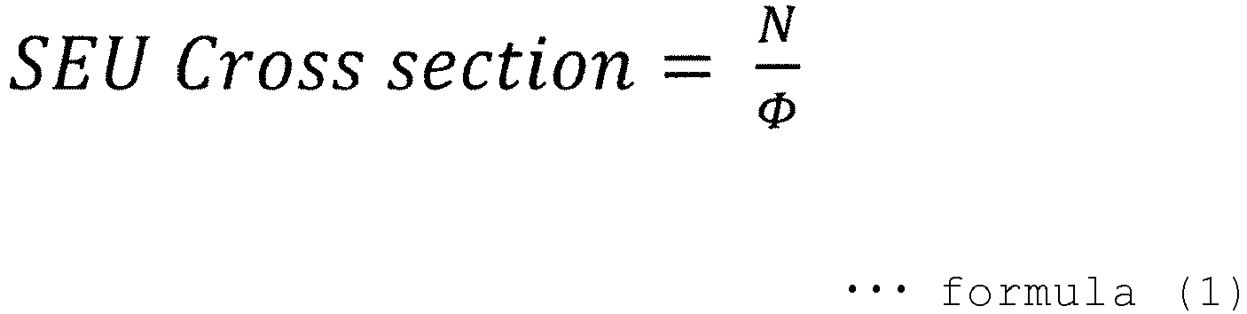
- an SEU cross section means a scale representing a rate at which particles cause an SEU to occur. It is assumed that the number of SEUs that have occurred when a semiconductor is irradiated with particles of a fluence ⁇ [n/cm 2 ] (total number of particles incident on a unit area) is N. Then, the SEU cross section is represented by the following formula (1).
- the time-of-flight method is a method in which the velocity of a particle is calculated by measuring the time required for flight of a certain distance, and this is converted into the particle energy.
- a time-of-flight method for a neutron as a kind of particle radiation will be described.
- the energy E of a neutron is proportional to the square of the velocity v of the neutron, and is expressed by the following formula (2).
- m is the mass of the neutron.
- the energy of the neutron can be specified by generating a pulse neutron by using an accelerator or a nuclear reactor, installing a detector at a fixed distance, and measuring the difference (the time-of-flight) between the time at which the pulse neutron is generated and the time at which the neutron is detected by the detector.
- the time-of-flight method is widely used as a method for obtaining neutron energy.
- Non-patent document 1 Eishi H. Ibe, "Terrestrial Radiation Effects in ULSI Devices and Electronic Systems", pp. 84-105, John Wiley & Sons Singapore Pte. Ltd, 2015 .
- a conventional monochromatic source is used as a method for specifying the energy of a particle which causes a soft error, especially in the case of a neutron, only the intermittent energy is generated, and it has been difficult to measure a continuous SEU cross section.
- Fig. 6 shows the relationship between the neutron energy and the time-of-flight in the case of a 20-m flight of a neutron. In this way, the time-of-flight of a high-energy particle is on the ns- ⁇ s order.
- a method for detecting the SEU there is a method for detecting a bit error in data by using an error-detecting code (CRC (Cyclic Redundancy Check), Parity, ECC (Error Correction Code), and the like).
- CRC Cyclic Redundancy Check
- Parity Parity
- ECC Error Correction Code
- the operating frequency is 1 GHz at the fastest, and the number of bits that can be read in 1 clock cycle is 64 bits at most. Therefore, about 15 ⁇ s is required to read out 1 Mbit.
- a configuration RAM of an FPGA field programmable gate array
- FPGA field programmable gate array
- the present invention is made in view of the above described problems, and an object of the present invention is to provide a nuclear reaction detection device, a method, and a program which can perform detection at high speed.
- a nuclear reaction detection device includes an FPGA (Field Programmable Gate Array) that is arranged in an environment in which particle radiation is incident, and includes a user circuit, the user circuit being configured to output a value different from that in a normal state, if an SEU (Single Event Upset) occurs in a semiconductor element included in the FPGA, and an abnormal operation detection unit that detects that an abnormal operation has occurred in the user circuit based on the value that is output from the user circuit in the FPGA.
- FPGA Field Programmable Gate Array
- the user circuit of the FPGA is configured such that the output behaves abnormally due to the occurrence of an SEU.
- the occurrence of an SEU can be detected in the order of the operation clock of the FPGA 100.
- the occurrence of an SEU can be detected at a high speed, and the measurement accuracy of the occurrence time of the SEU thereby becomes high.
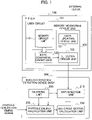
- FIG. 1 is a configuration diagram of a nuclear reaction detection device according to an embodiment of the present invention.
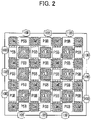
- FIG. 2 is a diagram for explaining an internal structure of an FPGA.
- FIG. 3 is a diagram for explaining an internal structure of a CLB of an FPGA, and the occurrence of an SEF.
- FIG. 4 is a diagram for explaining an internal structure of an SM of an FPGA, and the occurrence of an SEF.
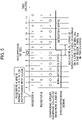
- FIG. 5 is a diagram for explaining operations of a memory monitoring circuit in an FPGA.
- the energy of the particle generating the SEU is specified using a time-of-flight method, and an SEU cross section of the energy is measured from the fluence of the particle with which an object has been irradiated. More specifically, as shown in FIG. 1 , the SEU is detected by using a user circuit 101 of an SRAM-type FPGA 100.
- the FPGA of the present embodiment is arranged in an environment in which particle radiation is incident, and is formed with a user circuit configured to output a value different from that in a normal state, if an SEU occurs in a semiconductor element included in the FPGA.
- the FPGA includes CLBs (Configuration Logic Block) which constitute the logic, IOBs (Input Output Block) which realize input/output functions, SMs (Switch Matrix) which are connection elements for realizing the connection between elements, and PSBs (Programmable Switch Box).
- CLBs Configuration Logic Block
- IOBs Input Output Block
- SMs Switch Matrix
- PSBs Programmable Switch Box
- each CLB includes an LUT (Look Up Table), and an FF (Flip Flop).
- the CLB can control an output value based on data of a CRAM (Configuration RAM) made of the SRAM of the LUT, and can configure various basic circuits. If an SEU occurs in the CRAM in the LUT, a circuit having a design different from the design intended by the user is formed, and a malfunction occurs.
- each SM (switch matrix) freely sets a wiring path by means of a pass-transistor.
- the pass-transistor being on/off is controlled by the CRAM made of the SRAM. If an SEU occurs in the CRAM, the wiring has a design different from the design intended by the user.
- an SEU occurs in the CLBs as logic units and the CRAMs of the SMs as connection units, the circuit immediately becomes an erroneous circuit, and may operate differently from the circuit operation designed by the user. This abnormal operation is called an SEF (Soft error failure) in this case.
- SEF Soft error failure
- the user circuit 101 capable of detecting an SEF will be described with reference to FIG. 1 .
- the user circuit 101 is configured by externally writing configuration data for the construction of the user circuit into the FPGA 100.
- the user circuit 101 includes a memory circuit unit 110, and a memory monitoring circuit unit 120.
- the memory monitoring circuit unit 120 monitors each piece of data included in the memory circuit unit 110 in an operation clock cycle of the FPGA 100, detects that a value of any of the pieces of data has changed, and outputs a detection result.
- This configuration enables the detection of an SEF in the order of the operation clock of the FPGA 100. Note that the frequency of the operation clock of the FPGA 100 does not necessarily coincide with an external clock input to the FPGA 100.
- the memory monitoring circuit unit 120 includes a data updating circuit unit 121, a data comparing circuit unit 122, and a detection circuit unit 123.
- the data updating circuit unit 121 changes all pieces of data of the memory circuit unit 110 with the same value and in a clock cycle.
- the data comparing circuit unit 122 compares the individual pieces of data of the memory circuit unit 110.
- the detection circuit unit 123 detects that the individual data values are no longer the same based on the comparison result by the data comparing circuit unit 122, and outputs a detection result.
- the memory circuit unit 110 includes as many registers as possible. Further, in the data updating circuit unit 121, a circuit is constructed for causing each register of the memory circuit unit 110 to repeat 0 ⁇ 1 ⁇ 0 ⁇ 1 at the maximum operating frequency (the timing can be converged).
- the data comparing circuit unit 122 compares and monitors the plurality of registers of the memory circuit unit 110.
- An example of the data comparing circuit unit 122 is an XOR circuit.
- the detection circuit unit 123 can detect an SEU at high speed by detecting an operation in which an output value of the data comparing circuit unit 122 does not change.
- the detection circuit unit 123 outputs an error detection signal after detecting the SEU.
- FIG. 5 illustrates an example of operations of the detection circuit unit 123. In FIG. 5 , only two registers A and B included in the memory circuit unit 110 are illustrated to simplify the explanation.
- the user circuit 101 can detect the occurrence of an SEU with a resolution on the order of nanoseconds. That is, the circuit can detect that an SEU has occurred within a time range of two clocks.
- the nuclear reaction detection device includes a nuclear reaction detection device body 200 that is electrically connected to the FPGA 100, and is arranged in an environment protected from the particle radiation.
- the nuclear reaction detection device body 200 includes an SEF detection unit 210, a particle energy calculation unit 220, an SEU cross section calculation unit 230, and a clocking unit 290.
- the nuclear reaction detection device body 200 is constituted from an information processor.
- the individual units of the nuclear reaction detection device body 200 may be mounted in any form, and may be constituted by dedicated hardware, may be constituted by a general-purpose device installed with a program, or may be constituted by any combination thereof.
- the SEF detection unit 210 detects the occurrence of an abnormal operation in the user circuit 101, that is, the occurrence of an SEF, based on an output value from the user circuit 101 of the FPGA 100. After detecting the occurrence of the SEF based on the error detection signal from the detection circuit unit 123, the SEF detection unit 210 recognizes the time at which the SEF occurred by acquiring the current time clocked by the clocking unit 290. The SEF detection unit 210 stores the occurrence of the SEF, and the time at which the SEF occurred in predetermined storage means (not illustrated) or outputs the same to an external device (not illustrated).
- the particle energy calculation unit 220 calculates particle energy by using the time-of-flight method based on the occurrence time of the abnormal operation measured by the SEF detection unit 210. Specifically, the particle energy calculation unit 220 calculates the difference between the time at which the acquired error detection signal from the detection circuit unit 123 is transmitted to the SEF detection unit 210, that is, the occurrence time of the SEF, and the time at which particles are generated. Accordingly, the particle energy calculation unit 220 can calculate the energy of the particles that generates the SEU and causes the SEF to occur. In order to acquire the time at which the particles are generated, the particle energy calculation unit 220 may detect the input of a particle generation timing signal from the external device, and acquire the current time at the time of detection from the clocking unit 290.
- the particle energy calculation unit 220 stores the calculated particle energy in a predetermined storage unit (not illustrated) or outputs the energy to the external device (not illustrated) .
- the time at which the particles are generated may be acquired from the external device, or stored in advance in a predetermined storage unit, and acquired from the storage unit.
- the SEU cross section calculation unit 230 calculates the SEU cross section of a CRAM. Specifically, the SEU cross section calculation unit 230 calculates the SEU cross section based on the number of occurrences of abnormal operations detected by the SEF detection unit 210. However, not all SEUs that occur in a CRAM cause an SEF. That is, an SEF may not be detected even if the SEU occurs in a CRAM that does not affect the circuit operation. SEFs vary depending on the user design, and thus it is not necessary to acquire the SEU cross section of an SEF, but it is necessary to acquire the SEU cross section of a CRAM.
- the number of SEUs including CRAMs which are not used (N) is calculated by using a CRC check function of the CRAMs, the SEF count distribution is set as the SEF probability distribution p(t), and the SEF energy probability distribution p(E) is calculated from the relationship between the energy and an arrival time illustrated in FIG. 6 .
- N the number of SEUs including CRAMs which are not used
- the user circuit 101 of the FPGA 100 is configured such that the output behaves abnormally due to the occurrence of an SEU.
- the occurrence of an SEU can be detected in the order of the operation clock of the FPGA 100.
- the occurrence of an SEU can be detected at a high speed, and the measurement accuracy of the occurrence time of the SEU thereby becomes high.
- This enables high-accuracy measurement of the energy of the particles causing an event such as an SEU.
- the occurrence rate of an event such as the SEU cross section for each continuous particle energy can be measured with high accuracy.
- the particle energy calculation unit 210 and the SEU cross section calculation unit 220 in the nuclear reaction detection device body 200 are any components, and the nuclear reaction detection device body 200 may have only one of them.
- the nuclear reaction detection device body 200 may further include an energy measuring unit for measuring the energy spectrum of a pulse particle source (pulse neutron source) by using the acquired occurrence rate of an event such as the SEU cross section.
- an energy measuring unit for measuring the energy spectrum of a pulse particle source (pulse neutron source) by using the acquired occurrence rate of an event such as the SEU cross section.
- the nuclear reaction detection device body 200 may further include energy detection means for detecting the energy in position information.
- the position information means a physical position (a spatial position) in the FPGA 100 at which an SEU has occurred.
- the position information can be acquired by, after detecting the occurrence of the SEU, comparing the configuration data for the user circuit construction with the user circuit 101, or by scanning data at each address of the memory circuit unit 110 to determine whether the data is appropriate.
- a neutron flux and a neutron fluence are measured by the neutron measuring device during the irradiation of the semiconductor.
- a neutron generation target is irradiated with proton pulses accelerated by an accelerator to generate neutrons.
- the device uses the user circuit in the FPGA to construct the register, and causes the register to be operated at an operation clock.
- An object is irradiated with neutrons, and the time-of-flight and the SEF count are observed.
- the total SEU cross section for the entire CRAM area, the total number of CRAM errors is observed. From the above, the SEU cross section is calculated.
- the present invention can be applied not only to an SRAM-type FPGA, but also to an EEPROM-type FPGA.
- the particle radiation is not limited to neutron radiation, and the present invention can be applied to other particle radiation, as long as an SEU occurs when other particle radiation is incident on the FPGA.
- the user circuit 101 is constructed of the memory circuit unit 110 and the memory monitoring circuit unit 120. However, another circuit may be adopted as long as an output value of another circuit changes owing to the occurrence of an abnormal operation due to the occurrence of an SEU.
- the above described nuclear reaction detection device body 200 can use a general-purpose computer system.
- the computer system includes a CPU (Central Processing Unit, a processor), a memory, a storage (HDD: Hard Disk Drive, SSD: Solid State Drive), a communication device, an input device, and an output device.
- the memory and storage are storage devices.
- each function of the nuclear reaction detection device body 200 is realized by the CPU executing a predetermined program loaded in the memory.
- the nuclear reaction detection device body 200 may be implemented by a single computer, or alternatively by a plurality of computers. Further, the nuclear reaction detection device body 200 may be a virtual machine mounted on a computer.
- the program for the nuclear reaction detection device body 200 can be stored in a computer-readable recording medium such as an HDD, SSD, USB (Universal Serial Bus) memory, CD (Compact Disc), or DVD (Digital Versatile Disc), or alternatively the program may be distributed via a network.
- a computer-readable recording medium such as an HDD, SSD, USB (Universal Serial Bus) memory, CD (Compact Disc), or DVD (Digital Versatile Disc), or alternatively the program may be distributed via a network.
Landscapes
- Physics & Mathematics (AREA)
- Engineering & Computer Science (AREA)
- General Physics & Mathematics (AREA)
- Spectroscopy & Molecular Physics (AREA)
- Life Sciences & Earth Sciences (AREA)
- Health & Medical Sciences (AREA)
- High Energy & Nuclear Physics (AREA)
- Molecular Biology (AREA)
- General Engineering & Computer Science (AREA)
- Theoretical Computer Science (AREA)
- Quality & Reliability (AREA)
- Computer Security & Cryptography (AREA)
- Computer Hardware Design (AREA)
- Computing Systems (AREA)
- Mathematical Physics (AREA)
- Measurement Of Radiation (AREA)
Abstract
Description
- The present invention relates to a technique for specifying an energy of a particle beam, and measuring an SEU cross section in the energy of the particle.
- In order to measure the energy dependency of an SEU (Single Event Upset) cross section, the SEU cross section was conventionally measured by irradiating an object with a particle beam of a specific energy. For example, CYRIC (Cyclotron and Radioisotope Center) and TSL (The Svedberg Lab.) are known as monochromatic/quasi-monochromatic neutron sources, and by generating only the specific energy, the SEU cross section according to the particles of the energy can be obtained (Non-patent document 1).
- An SEU in this case means an event in which a single particle (a neutron, proton, heavy particle, or the like) is incident on an LSI (Large Scale Integration) such as a memory, and data (a bit) stored in the LSI is inverted by charge generated by the nuclear reaction. An SEU is also called a soft error.
- Further, an SEU cross section means a scale representing a rate at which particles cause an SEU to occur. It is assumed that the number of SEUs that have occurred when a semiconductor is irradiated with particles of a fluence Φ [n/cm2] (total number of particles incident on a unit area) is N. Then, the SEU cross section is represented by the following formula (1).
- [Formula 1]
- Meanwhile, as a conventional method for detecting the energy of particle radiation, there is a time-of-flight method. The time-of-flight method is a method in which the velocity of a particle is calculated by measuring the time required for flight of a certain distance, and this is converted into the particle energy. As an example of the use of this method, for example, a time-of-flight method for a neutron as a kind of particle radiation will be described. The energy E of a neutron is proportional to the square of the velocity v of the neutron, and is expressed by the following formula (2). Here m is the mass of the neutron.
- [Formula 2]

- Therefore, the energy of the neutron can be specified by generating a pulse neutron by using an accelerator or a nuclear reactor, installing a detector at a fixed distance, and measuring the difference (the time-of-flight) between the time at which the pulse neutron is generated and the time at which the neutron is detected by the detector. In this way, the time-of-flight method is widely used as a method for obtaining neutron energy.
- Non-patent document 1: Eishi H. Ibe, "Terrestrial Radiation Effects in ULSI Devices and Electronic Systems", pp. 84-105, John Wiley & Sons Singapore Pte. Ltd, 2015.
- If a conventional monochromatic source is used as a method for specifying the energy of a particle which causes a soft error, especially in the case of a neutron, only the intermittent energy is generated, and it has been difficult to measure a continuous SEU cross section.
- The particles that cause the SEUs to occur are fast particles on the MeV order.
Fig. 6 shows the relationship between the neutron energy and the time-of-flight in the case of a 20-m flight of a neutron. In this way, the time-of-flight of a high-energy particle is on the ns-µs order. Meanwhile, as a method for detecting the SEU, there is a method for detecting a bit error in data by using an error-detecting code (CRC (Cyclic Redundancy Check), Parity, ECC (Error Correction Code), and the like). However, for example, in the case of an SRAM (Static Random Access Memory), the operating frequency is 1 GHz at the fastest, and the number of bits that can be read in 1 clock cycle is 64 bits at most. Therefore, about 15 µs is required to read out 1 Mbit. Further, a configuration RAM of an FPGA (field programmable gate array) can detect an error by using an error-detecting code, but several msec to several tens of msec are required to check the entire area. Thus, it has been difficult to detect the time-of-flight of high-energy particles by using an error-detecting code. - The present invention is made in view of the above described problems, and an object of the present invention is to provide a nuclear reaction detection device, a method, and a program which can perform detection at high speed.
- To achieve the above described object, a nuclear reaction detection device according to the present invention includes an FPGA (Field Programmable Gate Array) that is arranged in an environment in which particle radiation is incident, and includes a user circuit, the user circuit being configured to output a value different from that in a normal state, if an SEU (Single Event Upset) occurs in a semiconductor element included in the FPGA, and an abnormal operation detection unit that detects that an abnormal operation has occurred in the user circuit based on the value that is output from the user circuit in the FPGA.
- According to the present invention, the user circuit of the FPGA is configured such that the output behaves abnormally due to the occurrence of an SEU. Thus, the occurrence of an SEU can be detected in the order of the operation clock of the
FPGA 100. In other words, the occurrence of an SEU can be detected at a high speed, and the measurement accuracy of the occurrence time of the SEU thereby becomes high. -
- [
Fig. 1] FIG. 1 is a diagram illustrating a configuration of a nuclear reaction detection device according to an embodiment of the present invention. - [
Fig. 2] FIG. 2 is a diagram for explaining an internal structure of an FPGA. - [
Fig. 3] FIG. 3 is a diagram for explaining an internal structure of a CLB of an FPGA, and the occurrence of an SEF. - [
Fig. 4] FIG. 4 is a diagram for explaining an internal structure of an SM in an FPGA, and the occurrence of an SEF. - [
Fig. 5] FIG. 5 is a diagram for explaining operations of a memory monitoring circuit in an FPGA. - [
Fig. 6] FIG. 6 is a diagram showing the relationship between neutron energy and time-of-flight. - A nuclear reaction detection device according to an embodiment of the present invention will be described with reference to
FIGS. 1 to 5 .FIG. 1 is a configuration diagram of a nuclear reaction detection device according to an embodiment of the present invention.FIG. 2 is a diagram for explaining an internal structure of an FPGA.FIG. 3 is a diagram for explaining an internal structure of a CLB of an FPGA, and the occurrence of an SEF.FIG. 4 is a diagram for explaining an internal structure of an SM of an FPGA, and the occurrence of an SEF.FIG. 5 is a diagram for explaining operations of a memory monitoring circuit in an FPGA. - In this embodiment, by detecting an error caused by an SEU in the order of nanoseconds, the energy of the particle generating the SEU is specified using a time-of-flight method, and an SEU cross section of the energy is measured from the fluence of the particle with which an object has been irradiated. More specifically, as shown in
FIG. 1 , the SEU is detected by using auser circuit 101 of an SRAM-type FPGA 100. The FPGA of the present embodiment is arranged in an environment in which particle radiation is incident, and is formed with a user circuit configured to output a value different from that in a normal state, if an SEU occurs in a semiconductor element included in the FPGA. - First, the general internal structure of the FPGA, and the principle of detecting an SEU will be described. As shown in
FIG. 2 , the FPGA includes CLBs (Configuration Logic Block) which constitute the logic, IOBs (Input Output Block) which realize input/output functions, SMs (Switch Matrix) which are connection elements for realizing the connection between elements, and PSBs (Programmable Switch Box). - As shown in
FIG. 3 , each CLB includes an LUT (Look Up Table), and an FF (Flip Flop). The CLB can control an output value based on data of a CRAM (Configuration RAM) made of the SRAM of the LUT, and can configure various basic circuits. If an SEU occurs in the CRAM in the LUT, a circuit having a design different from the design intended by the user is formed, and a malfunction occurs. - As shown in
FIG. 4 , each SM (switch matrix) freely sets a wiring path by means of a pass-transistor. The pass-transistor being on/off is controlled by the CRAM made of the SRAM. If an SEU occurs in the CRAM, the wiring has a design different from the design intended by the user. - As described above, if an SEU occurs in the CLBs as logic units and the CRAMs of the SMs as connection units, the circuit immediately becomes an erroneous circuit, and may operate differently from the circuit operation designed by the user. This abnormal operation is called an SEF (Soft error failure) in this case. The detection of an SEF enables a high-speed detection of an SEU.
- An example of the
user circuit 101 capable of detecting an SEF will be described with reference toFIG. 1 . As is well known, theuser circuit 101 is configured by externally writing configuration data for the construction of the user circuit into theFPGA 100. - In the example of
FIG. 1 , theuser circuit 101 includes amemory circuit unit 110, and a memorymonitoring circuit unit 120. The memorymonitoring circuit unit 120 monitors each piece of data included in thememory circuit unit 110 in an operation clock cycle of theFPGA 100, detects that a value of any of the pieces of data has changed, and outputs a detection result. This configuration enables the detection of an SEF in the order of the operation clock of theFPGA 100. Note that the frequency of the operation clock of theFPGA 100 does not necessarily coincide with an external clock input to theFPGA 100. - As a more specific example, the memory
monitoring circuit unit 120 includes a data updatingcircuit unit 121, a data comparingcircuit unit 122, and adetection circuit unit 123. The data updatingcircuit unit 121 changes all pieces of data of thememory circuit unit 110 with the same value and in a clock cycle. The data comparingcircuit unit 122 compares the individual pieces of data of thememory circuit unit 110. Thedetection circuit unit 123 detects that the individual data values are no longer the same based on the comparison result by the data comparingcircuit unit 122, and outputs a detection result. - As a more specific example, the
memory circuit unit 110 includes as many registers as possible. Further, in the data updatingcircuit unit 121, a circuit is constructed for causing each register of thememory circuit unit 110 to repeat 0 → 1 → 0 → 1 at the maximum operating frequency (the timing can be converged). The data comparingcircuit unit 122 compares and monitors the plurality of registers of thememory circuit unit 110. An example of the data comparingcircuit unit 122 is an XOR circuit. - If an SEU occurs, the registers do not function correctly, and thus the value does not change. The
detection circuit unit 123 can detect an SEU at high speed by detecting an operation in which an output value of the data comparingcircuit unit 122 does not change. Thedetection circuit unit 123 outputs an error detection signal after detecting the SEU.FIG. 5 illustrates an example of operations of thedetection circuit unit 123. InFIG. 5 , only two registers A and B included in thememory circuit unit 110 are illustrated to simplify the explanation. As illustrated inFIG. 5 , theuser circuit 101 can detect the occurrence of an SEU with a resolution on the order of nanoseconds. That is, the circuit can detect that an SEU has occurred within a time range of two clocks. - As illustrated in
FIG. 1 , the nuclear reaction detection device according to the present embodiment includes a nuclear reactiondetection device body 200 that is electrically connected to theFPGA 100, and is arranged in an environment protected from the particle radiation. The nuclear reactiondetection device body 200 includes anSEF detection unit 210, a particleenergy calculation unit 220, an SEU crosssection calculation unit 230, and aclocking unit 290. The nuclear reactiondetection device body 200 is constituted from an information processor. The individual units of the nuclear reactiondetection device body 200 may be mounted in any form, and may be constituted by dedicated hardware, may be constituted by a general-purpose device installed with a program, or may be constituted by any combination thereof. - The SEF detection unit 210 (an abnormal operation detection unit) detects the occurrence of an abnormal operation in the
user circuit 101, that is, the occurrence of an SEF, based on an output value from theuser circuit 101 of theFPGA 100. After detecting the occurrence of the SEF based on the error detection signal from thedetection circuit unit 123, theSEF detection unit 210 recognizes the time at which the SEF occurred by acquiring the current time clocked by theclocking unit 290. TheSEF detection unit 210 stores the occurrence of the SEF, and the time at which the SEF occurred in predetermined storage means (not illustrated) or outputs the same to an external device (not illustrated). - The particle
energy calculation unit 220 calculates particle energy by using the time-of-flight method based on the occurrence time of the abnormal operation measured by theSEF detection unit 210. Specifically, the particleenergy calculation unit 220 calculates the difference between the time at which the acquired error detection signal from thedetection circuit unit 123 is transmitted to theSEF detection unit 210, that is, the occurrence time of the SEF, and the time at which particles are generated. Accordingly, the particleenergy calculation unit 220 can calculate the energy of the particles that generates the SEU and causes the SEF to occur. In order to acquire the time at which the particles are generated, the particleenergy calculation unit 220 may detect the input of a particle generation timing signal from the external device, and acquire the current time at the time of detection from theclocking unit 290. The particleenergy calculation unit 220 stores the calculated particle energy in a predetermined storage unit (not illustrated) or outputs the energy to the external device (not illustrated) . The time at which the particles are generated may be acquired from the external device, or stored in advance in a predetermined storage unit, and acquired from the storage unit. - The SEU cross
section calculation unit 230 calculates the SEU cross section of a CRAM. Specifically, the SEU crosssection calculation unit 230 calculates the SEU cross section based on the number of occurrences of abnormal operations detected by theSEF detection unit 210. However, not all SEUs that occur in a CRAM cause an SEF. That is, an SEF may not be detected even if the SEU occurs in a CRAM that does not affect the circuit operation. SEFs vary depending on the user design, and thus it is not necessary to acquire the SEU cross section of an SEF, but it is necessary to acquire the SEU cross section of a CRAM. - To obtain an absolute value of the SEU cross section of a CRAM, correction is necessary. In order to perform the correction, the number of SEUs including CRAMs which are not used (N) is calculated by using a CRC check function of the CRAMs, the SEF count distribution is set as the SEF probability distribution p(t), and the SEF energy probability distribution p(E) is calculated from the relationship between the energy and an arrival time illustrated in
FIG. 6 . By multiplying N by p (E), an NSEU (E) absolute value which serves as the distribution of the number of SEU occurrences for each energy can be calculated. Finally, the SEU cross section for each energy is calculated from the fluence Φ(E) for each energy measured with a neutron measuring device. - As described above, according to the nuclear reaction detection device of the present embodiment, the
user circuit 101 of theFPGA 100 is configured such that the output behaves abnormally due to the occurrence of an SEU. Thus, the occurrence of an SEU can be detected in the order of the operation clock of theFPGA 100. In other words, the occurrence of an SEU can be detected at a high speed, and the measurement accuracy of the occurrence time of the SEU thereby becomes high. This enables high-accuracy measurement of the energy of the particles causing an event such as an SEU. Further, the occurrence rate of an event such as the SEU cross section for each continuous particle energy can be measured with high accuracy. - The particle
energy calculation unit 210 and the SEU crosssection calculation unit 220 in the nuclear reactiondetection device body 200 are any components, and the nuclear reactiondetection device body 200 may have only one of them. - The nuclear reaction
detection device body 200 may further include an energy measuring unit for measuring the energy spectrum of a pulse particle source (pulse neutron source) by using the acquired occurrence rate of an event such as the SEU cross section. - The nuclear reaction
detection device body 200 may further include energy detection means for detecting the energy in position information. The position information means a physical position (a spatial position) in theFPGA 100 at which an SEU has occurred. The position information can be acquired by, after detecting the occurrence of the SEU, comparing the configuration data for the user circuit construction with theuser circuit 101, or by scanning data at each address of thememory circuit unit 110 to determine whether the data is appropriate. - An example of measuring the SEU cross section with neutrons will be given.
- In a neutron irradiation field, a neutron flux and a neutron fluence are measured by the neutron measuring device during the irradiation of the semiconductor. A neutron generation target is irradiated with proton pulses accelerated by an accelerator to generate neutrons. The moment at which the proton pulse hits the neutron generation target is the time at which the neutrons are generated, and this corresponds to t = 0 in the time-of-flight method. The time-of-flight is measured by taking the difference between a timing signal indicating t = 0 and a timing signal for the detection of an SEF, and this can be converted into neutron energy.
- The device uses the user circuit in the FPGA to construct the register, and causes the register to be operated at an operation clock. An object is irradiated with neutrons, and the time-of-flight and the SEF count are observed. In the measurement of the total SEU cross section for the entire CRAM area, the total number of CRAM errors is observed. From the above, the SEU cross section is calculated.
- Although one embodiment of the present invention has been described in detail above, the present invention is not limited to the above described embodiment, and various improvements and modifications may be made without departing from the gist of the present invention.
- For example, the present invention can be applied not only to an SRAM-type FPGA, but also to an EEPROM-type FPGA. Further, the particle radiation is not limited to neutron radiation, and the present invention can be applied to other particle radiation, as long as an SEU occurs when other particle radiation is incident on the FPGA.
- The
user circuit 101 is constructed of thememory circuit unit 110 and the memorymonitoring circuit unit 120. However, another circuit may be adopted as long as an output value of another circuit changes owing to the occurrence of an abnormal operation due to the occurrence of an SEU. - The above described nuclear reaction
detection device body 200 can use a general-purpose computer system. For example, the computer system includes a CPU (Central Processing Unit, a processor), a memory, a storage (HDD: Hard Disk Drive, SSD: Solid State Drive), a communication device, an input device, and an output device. The memory and storage are storage devices. In this computer system, each function of the nuclear reactiondetection device body 200 is realized by the CPU executing a predetermined program loaded in the memory. Further, the nuclear reactiondetection device body 200 may be implemented by a single computer, or alternatively by a plurality of computers. Further, the nuclear reactiondetection device body 200 may be a virtual machine mounted on a computer. The program for the nuclear reactiondetection device body 200 can be stored in a computer-readable recording medium such as an HDD, SSD, USB (Universal Serial Bus) memory, CD (Compact Disc), or DVD (Digital Versatile Disc), or alternatively the program may be distributed via a network. -
- 100
- FPGA
- 101
- User circuit
- 110
- Memory circuit unit
- 120
- Memory monitoring circuit unit
- 121
- Data updating circuit unit
- 122
- Data comparing circuit unit
- 123
- Detection circuit unit
- 200
- Nuclear reaction detection device body
- 210
- SEF detection unit
- 220
- Particle energy calculation unit
- 230
- SEU cross section calculation unit
- 290
- Clocking unit
Claims (8)
- A nuclear reaction detection device comprising:an FPGA (Field Programmable Gate Array) that is arranged in an environment in which particle radiation is incident, and includes a user circuit, the user circuit being configured to output a value different from that in a normal state, if an SEU (Single Event Upset) occurs in a semiconductor element included in the FPGA; andan abnormal operation detection unit that detects that an abnormal operation has occurred in the user circuit based on the value that is output from the user circuit in the FPGA.
- The nuclear reaction detection device according to claim 1, wherein
the user circuit includes a memory circuit unit, and a memory monitoring circuit unit that monitors each of all pieces of data included in the memory circuit unit in a clock cycle of the FPGA, and detects a change in a value of any of the pieces of data to output a detection result. - The nuclear reaction detection device according to claim 2, wherein
the memory monitoring circuit unit includes a data updating circuit unit that changes all pieces of data of the memory circuit unit with a same value and in the clock cycle, a data comparing circuit unit that compares the individual pieces of data of the memory circuit unit, and a detection circuit unit that detects that the values of the individual pieces of data are no longer the same based on a comparison result by the data comparing circuit unit, and outputs a detection result. - The nuclear reaction detection device according to any one of claims 1 to 3, comprising:
an SEU cross section calculation unit that calculates an SEU cross section based on the number of occurrences of the abnormal operation detected by the abnormal operation detection unit. - The nuclear reaction detection device according to any one of claims 1 to 3, comprising:
a particle energy calculation unit that calculates particle energy by using a time-of-flight method based on an occurrence time of the abnormal operation measured by the abnormal operation detection unit. - The nuclear reaction detection device according to any one of claims 1 to 5, wherein the FPGA is an SRAM-type FPGA.
- A nuclear reaction detection method comprising:a step of arranging, in an environment in which particle radiation is incident, an FPGA (Field Programmable Gate Array) that includes a user circuit, the user circuit being configured to output a value different from that in a normal state, if an SEU (Single Event Upset) occurs in a semiconductor element included in the FPGA; andan abnormal operation detection step of detecting that an abnormal operation has occurred in the user circuit based on the output value from the user circuit in the FPGA.
- A nuclear reaction detection program for causing a computer to function as the abnormal operation detection unit of the nuclear reaction detection device according to any one of claims 1 to 6.
Applications Claiming Priority (2)
| Application Number | Priority Date | Filing Date | Title |
|---|---|---|---|
| JP2019125192 | 2019-07-04 | ||
| PCT/JP2020/026274 WO2021002469A1 (en) | 2019-07-04 | 2020-07-03 | Nuclear reaction detection device, method, and program |
Publications (4)
| Publication Number | Publication Date |
|---|---|
| EP3995864A1 true EP3995864A1 (en) | 2022-05-11 |
| EP3995864A4 EP3995864A4 (en) | 2023-07-05 |
| EP3995864B1 EP3995864B1 (en) | 2025-09-03 |
| EP3995864B8 EP3995864B8 (en) | 2025-10-15 |
Family
ID=74100394
Family Applications (1)
| Application Number | Title | Priority Date | Filing Date |
|---|---|---|---|
| EP20834787.2A Active EP3995864B8 (en) | 2019-07-04 | 2020-07-03 | Nuclear reaction detection device, method, and program |
Country Status (5)
| Country | Link |
|---|---|
| US (1) | US12158552B2 (en) |
| EP (1) | EP3995864B8 (en) |
| JP (1) | JP7181566B2 (en) |
| CN (1) | CN114127587A (en) |
| WO (1) | WO2021002469A1 (en) |
Families Citing this family (3)
| Publication number | Priority date | Publication date | Assignee | Title |
|---|---|---|---|---|
| WO2021229678A1 (en) * | 2020-05-12 | 2021-11-18 | 日本電信電話株式会社 | Nuclear reaction detection device, nuclear reaction detection method, and nuclear reaction detection program |
| JP7687569B2 (en) * | 2022-03-23 | 2025-06-03 | 日本電信電話株式会社 | SEU cross section estimation device, SEU cross section estimation method, and SEU cross section estimation program |
| CN118377645B (en) * | 2024-06-24 | 2024-08-27 | 之江实验室 | An abnormality handling system, method and detection device for space environment |
Family Cites Families (10)
| Publication number | Priority date | Publication date | Assignee | Title |
|---|---|---|---|---|
| US7800439B2 (en) * | 2006-10-27 | 2010-09-21 | Ut-Battelle, Llc | High speed preamplifier circuit, detection electronics, and radiation detection systems therefrom |
| US7499308B2 (en) * | 2007-03-21 | 2009-03-03 | International Business Machines Corporation | Programmable heavy-ion sensing device for accelerated DRAM soft error detection |
| CN101561477A (en) * | 2009-05-15 | 2009-10-21 | 中国人民解放军国防科学技术大学 | Method and device for testing single event upset in in-field programmable logic gate array |
| CN203801141U (en) * | 2013-12-27 | 2014-08-27 | 清华大学 | Nuclide identification system and photoneutron emitter |
| US9672880B2 (en) * | 2014-06-16 | 2017-06-06 | Honeywell International Inc. | Radiation upset detection |
| CN104893709A (en) * | 2015-06-09 | 2015-09-09 | 西北核技术研究所 | Surface treatment method for scintillator |
| CN106385757A (en) * | 2016-09-18 | 2017-02-08 | 中国科学院上海应用物理研究所 | Neutron generation target |
| CN106842282B (en) | 2016-12-29 | 2018-06-29 | 西北核技术研究所 | A kind of method that neutron irradiation environmental monitoring is carried out using SRAM memory |
| JP6873794B2 (en) | 2017-04-05 | 2021-05-19 | 株式会社日立製作所 | Neutron intensity monitoring system and method |
| CN108287302A (en) * | 2018-01-29 | 2018-07-17 | 北京卫星环境工程研究所 | The single particle effect detection circuit structure of space-oriented radiation environment |
-
2020
- 2020-07-03 US US17/624,689 patent/US12158552B2/en active Active
- 2020-07-03 WO PCT/JP2020/026274 patent/WO2021002469A1/en not_active Ceased
- 2020-07-03 CN CN202080048991.4A patent/CN114127587A/en active Pending
- 2020-07-03 EP EP20834787.2A patent/EP3995864B8/en active Active
- 2020-07-03 JP JP2021529203A patent/JP7181566B2/en active Active
Also Published As
| Publication number | Publication date |
|---|---|
| US12158552B2 (en) | 2024-12-03 |
| EP3995864B8 (en) | 2025-10-15 |
| EP3995864A4 (en) | 2023-07-05 |
| CN114127587A (en) | 2022-03-01 |
| US20220260735A1 (en) | 2022-08-18 |
| JPWO2021002469A1 (en) | 2021-01-07 |
| EP3995864B1 (en) | 2025-09-03 |
| JP7181566B2 (en) | 2022-12-01 |
| WO2021002469A1 (en) | 2021-01-07 |
Similar Documents
| Publication | Publication Date | Title |
|---|---|---|
| Seifert et al. | Impact of scaling on soft-error rates in commercial microprocessors | |
| US12158552B2 (en) | Nuclear reaction detection device, method and program | |
| Nidhin et al. | Understanding radiation effects in SRAM-based field programmable gate arrays for implementing instrumentation and control systems of nuclear power plants | |
| She et al. | SEU tolerant memory using error correction code | |
| US20140203836A1 (en) | Method of characterizing the sensitivity of an electronic component subjected to irradiation conditions | |
| Chen et al. | Design of SRAM-based low-cost SEU monitor for self-adaptive multiprocessing systems | |
| CN110018514A (en) | A kind of inversion algorithm of neutron energy spectrum detector and measurement neutron energy spectrum based on SRAM | |
| Scialdone et al. | FPGA qualification and failure rate estimation methodology for LHC environments using benchmarks test circuits | |
| Gao et al. | Design of FPGA-implemented Reed-Solomon erasure code (RS-EC) decoders with fault detection and location on user memory | |
| Heijmen et al. | Soft-error rate testing of deep-submicron integrated circuits | |
| Kumar et al. | Analysis of neutron-induced multibit-upset clusters in a 14-nm flip-flop array | |
| Ming et al. | Reliability of memories protected by multibit error correction codes against MBUs | |
| Smith | Single event upset mitigation by means of a sequential circuit state freeze | |
| JP7339587B2 (en) | NUCLEAR REACTION DETECTION DEVICE, NUCLEAR REACTION DETECTION METHOD AND NUCLEAR REACTION DETECTION PROGRAM | |
| Veeravalli et al. | Architecture and design analysis of a digital single-event transient/upset measurement chip | |
| Brusati et al. | Mitigated FPGA design of multi-gigabit transceivers for application in high radiation environments of High Energy Physics experiments | |
| Alexandrescu et al. | Fault injection and fault tolerance methodologies for assessing device robustness and mitigating against ionizing radiation | |
| Ahmad et al. | Fault-tolerant reconfigurable 32-bit alu for space applications | |
| Sooraj et al. | Hamming 3 algorithm for improving the reliability of SRAM based FPGAs | |
| Leong et al. | Fast radiation monitoring in FPGA-based designs | |
| Bruni et al. | Power dissipation effects on 28nm FPGA-based System on Chips neutron sensitivity | |
| Batista et al. | SEU mitigation exploratory tests in a ITER related FPGA | |
| Clark et al. | Methodical design approaches to radiation effects analysis and mitigation in flip-flop circuits | |
| Chen et al. | Analysis of affecting factors in neutron interactions with gate oxide in CMOS transistors | |
| Celis | Statistical method for extracting radiation-induced multi-cell upsets and anomalies in SRAM-Based FPGAs |
Legal Events
| Date | Code | Title | Description |
|---|---|---|---|
| STAA | Information on the status of an ep patent application or granted ep patent |
Free format text: STATUS: THE INTERNATIONAL PUBLICATION HAS BEEN MADE |
|
| PUAI | Public reference made under article 153(3) epc to a published international application that has entered the european phase |
Free format text: ORIGINAL CODE: 0009012 |
|
| STAA | Information on the status of an ep patent application or granted ep patent |
Free format text: STATUS: REQUEST FOR EXAMINATION WAS MADE |
|
| 17P | Request for examination filed |
Effective date: 20220119 |
|
| AK | Designated contracting states |
Kind code of ref document: A1 Designated state(s): AL AT BE BG CH CY CZ DE DK EE ES FI FR GB GR HR HU IE IS IT LI LT LU LV MC MK MT NL NO PL PT RO RS SE SI SK SM TR |
|
| DAV | Request for validation of the european patent (deleted) | ||
| DAX | Request for extension of the european patent (deleted) | ||
| A4 | Supplementary search report drawn up and despatched |
Effective date: 20230607 |
|
| RIC1 | Information provided on ipc code assigned before grant |
Ipc: G06F 11/00 20060101ALI20230601BHEP Ipc: G01T 1/24 20060101AFI20230601BHEP |
|
| GRAP | Despatch of communication of intention to grant a patent |
Free format text: ORIGINAL CODE: EPIDOSNIGR1 |
|
| STAA | Information on the status of an ep patent application or granted ep patent |
Free format text: STATUS: GRANT OF PATENT IS INTENDED |
|
| INTG | Intention to grant announced |
Effective date: 20250228 |
|
| GRAS | Grant fee paid |
Free format text: ORIGINAL CODE: EPIDOSNIGR3 |
|
| GRAA | (expected) grant |
Free format text: ORIGINAL CODE: 0009210 |
|
| STAA | Information on the status of an ep patent application or granted ep patent |
Free format text: STATUS: THE PATENT HAS BEEN GRANTED |
|
| REG | Reference to a national code |
Ref country code: DE Ref legal event code: R081 Ref document number: 602020058168 Country of ref document: DE Owner name: NATIONAL UNIVERSITY CORPORATION HOKKAIDO UNIVE, JP Free format text: FORMER OWNERS: NATIONAL UNIVERSITY CORPORATION HOKKAIDO UNIVERSITY, SAPPORO, HOKKAIDO, JP; NATIONAL UNIVERSITY CORPORATION TOKAI NATIONAL HIGHER EDUCATION AND RESEARCH SYSTEM, NAGOYA-SHI, AICHI, JP; NIPPON TELEGRAPH AND TELEPHONE CORPORATION, TOKYO, JP Ref country code: DE Ref legal event code: R081 Ref document number: 602020058168 Country of ref document: DE Owner name: NATIONAL UNIVERSITY CORPORATION TOKAI NATIONAL, JP Free format text: FORMER OWNERS: NATIONAL UNIVERSITY CORPORATION HOKKAIDO UNIVERSITY, SAPPORO, HOKKAIDO, JP; NATIONAL UNIVERSITY CORPORATION TOKAI NATIONAL HIGHER EDUCATION AND RESEARCH SYSTEM, NAGOYA-SHI, AICHI, JP; NIPPON TELEGRAPH AND TELEPHONE CORPORATION, TOKYO, JP Ref country code: DE Ref legal event code: R081 Ref document number: 602020058168 Country of ref document: DE Owner name: NTT, INC., JP Free format text: FORMER OWNERS: NATIONAL UNIVERSITY CORPORATION HOKKAIDO UNIVERSITY, SAPPORO, HOKKAIDO, JP; NATIONAL UNIVERSITY CORPORATION TOKAI NATIONAL HIGHER EDUCATION AND RESEARCH SYSTEM, NAGOYA-SHI, AICHI, JP; NIPPON TELEGRAPH AND TELEPHONE CORPORATION, TOKYO, JP |
|
| AK | Designated contracting states |
Kind code of ref document: B1 Designated state(s): AL AT BE BG CH CY CZ DE DK EE ES FI FR GB GR HR HU IE IS IT LI LT LU LV MC MK MT NL NO PL PT RO RS SE SI SK SM TR |
|
| REG | Reference to a national code |
Ref country code: CH Ref legal event code: EP |
|
| REG | Reference to a national code |
Ref country code: DE Ref legal event code: R096 Ref document number: 602020058168 Country of ref document: DE |
|
| REG | Reference to a national code |
Ref country code: CH Ref legal event code: PK Free format text: BERICHTIGUNG B8 |
|
| RAP4 | Party data changed (patent owner data changed or rights of a patent transferred) |
Owner name: NTT, INC. Owner name: NATIONAL UNIVERSITY CORPORATIONHOKKAIDO UNIVERSITY Owner name: NATIONAL UNIVERSITY CORPORATION TOKAI NATIONALHIGHER EDUCATION AND RESEARCH SYSTEM |
|
| REG | Reference to a national code |
Ref country code: IE Ref legal event code: FG4D |
|
| REG | Reference to a national code |
Ref country code: NL Ref legal event code: MP Effective date: 20250903 |
|
| PG25 | Lapsed in a contracting state [announced via postgrant information from national office to epo] |
Ref country code: NO Free format text: LAPSE BECAUSE OF FAILURE TO SUBMIT A TRANSLATION OF THE DESCRIPTION OR TO PAY THE FEE WITHIN THE PRESCRIBED TIME-LIMIT Effective date: 20251203 |
|
| REG | Reference to a national code |
Ref country code: LT Ref legal event code: MG9D |
|
| PG25 | Lapsed in a contracting state [announced via postgrant information from national office to epo] |
Ref country code: FI Free format text: LAPSE BECAUSE OF FAILURE TO SUBMIT A TRANSLATION OF THE DESCRIPTION OR TO PAY THE FEE WITHIN THE PRESCRIBED TIME-LIMIT Effective date: 20250903 |
|
| PG25 | Lapsed in a contracting state [announced via postgrant information from national office to epo] |
Ref country code: HR Free format text: LAPSE BECAUSE OF FAILURE TO SUBMIT A TRANSLATION OF THE DESCRIPTION OR TO PAY THE FEE WITHIN THE PRESCRIBED TIME-LIMIT Effective date: 20250903 |
|
| PG25 | Lapsed in a contracting state [announced via postgrant information from national office to epo] |
Ref country code: GR Free format text: LAPSE BECAUSE OF FAILURE TO SUBMIT A TRANSLATION OF THE DESCRIPTION OR TO PAY THE FEE WITHIN THE PRESCRIBED TIME-LIMIT Effective date: 20251204 |
|
| PG25 | Lapsed in a contracting state [announced via postgrant information from national office to epo] |
Ref country code: SE Free format text: LAPSE BECAUSE OF FAILURE TO SUBMIT A TRANSLATION OF THE DESCRIPTION OR TO PAY THE FEE WITHIN THE PRESCRIBED TIME-LIMIT Effective date: 20250903 |
|
| PG25 | Lapsed in a contracting state [announced via postgrant information from national office to epo] |
Ref country code: LV Free format text: LAPSE BECAUSE OF FAILURE TO SUBMIT A TRANSLATION OF THE DESCRIPTION OR TO PAY THE FEE WITHIN THE PRESCRIBED TIME-LIMIT Effective date: 20250903 |
|
| PG25 | Lapsed in a contracting state [announced via postgrant information from national office to epo] |
Ref country code: BG Free format text: LAPSE BECAUSE OF FAILURE TO SUBMIT A TRANSLATION OF THE DESCRIPTION OR TO PAY THE FEE WITHIN THE PRESCRIBED TIME-LIMIT Effective date: 20250903 Ref country code: PL Free format text: LAPSE BECAUSE OF FAILURE TO SUBMIT A TRANSLATION OF THE DESCRIPTION OR TO PAY THE FEE WITHIN THE PRESCRIBED TIME-LIMIT Effective date: 20250903 |
|
| PG25 | Lapsed in a contracting state [announced via postgrant information from national office to epo] |
Ref country code: RS Free format text: LAPSE BECAUSE OF FAILURE TO SUBMIT A TRANSLATION OF THE DESCRIPTION OR TO PAY THE FEE WITHIN THE PRESCRIBED TIME-LIMIT Effective date: 20251203 |
|
| PG25 | Lapsed in a contracting state [announced via postgrant information from national office to epo] |
Ref country code: ES Free format text: LAPSE BECAUSE OF FAILURE TO SUBMIT A TRANSLATION OF THE DESCRIPTION OR TO PAY THE FEE WITHIN THE PRESCRIBED TIME-LIMIT Effective date: 20250903 |
|
| REG | Reference to a national code |
Ref country code: AT Ref legal event code: MK05 Ref document number: 1833686 Country of ref document: AT Kind code of ref document: T Effective date: 20250903 |
|
| PG25 | Lapsed in a contracting state [announced via postgrant information from national office to epo] |
Ref country code: NL Free format text: LAPSE BECAUSE OF FAILURE TO SUBMIT A TRANSLATION OF THE DESCRIPTION OR TO PAY THE FEE WITHIN THE PRESCRIBED TIME-LIMIT Effective date: 20250903 |
|
| PG25 | Lapsed in a contracting state [announced via postgrant information from national office to epo] |
Ref country code: SM Free format text: LAPSE BECAUSE OF FAILURE TO SUBMIT A TRANSLATION OF THE DESCRIPTION OR TO PAY THE FEE WITHIN THE PRESCRIBED TIME-LIMIT Effective date: 20250903 |
|
| PG25 | Lapsed in a contracting state [announced via postgrant information from national office to epo] |
Ref country code: AT Free format text: LAPSE BECAUSE OF FAILURE TO SUBMIT A TRANSLATION OF THE DESCRIPTION OR TO PAY THE FEE WITHIN THE PRESCRIBED TIME-LIMIT Effective date: 20250903 |
|
| PG25 | Lapsed in a contracting state [announced via postgrant information from national office to epo] |
Ref country code: IS Free format text: LAPSE BECAUSE OF FAILURE TO SUBMIT A TRANSLATION OF THE DESCRIPTION OR TO PAY THE FEE WITHIN THE PRESCRIBED TIME-LIMIT Effective date: 20260103 |
|
| PG25 | Lapsed in a contracting state [announced via postgrant information from national office to epo] |
Ref country code: PT Free format text: LAPSE BECAUSE OF FAILURE TO SUBMIT A TRANSLATION OF THE DESCRIPTION OR TO PAY THE FEE WITHIN THE PRESCRIBED TIME-LIMIT Effective date: 20260105 Ref country code: CZ Free format text: LAPSE BECAUSE OF FAILURE TO SUBMIT A TRANSLATION OF THE DESCRIPTION OR TO PAY THE FEE WITHIN THE PRESCRIBED TIME-LIMIT Effective date: 20250903 |
|
| PG25 | Lapsed in a contracting state [announced via postgrant information from national office to epo] |
Ref country code: SK Free format text: LAPSE BECAUSE OF FAILURE TO SUBMIT A TRANSLATION OF THE DESCRIPTION OR TO PAY THE FEE WITHIN THE PRESCRIBED TIME-LIMIT Effective date: 20250903 |
|
| REG | Reference to a national code |
Ref country code: DE Ref legal event code: R097 Ref document number: 602020058168 Country of ref document: DE |
|
| PG25 | Lapsed in a contracting state [announced via postgrant information from national office to epo] |
Ref country code: LT Free format text: LAPSE BECAUSE OF FAILURE TO SUBMIT A TRANSLATION OF THE DESCRIPTION OR TO PAY THE FEE WITHIN THE PRESCRIBED TIME-LIMIT Effective date: 20250903 |
|
| PG25 | Lapsed in a contracting state [announced via postgrant information from national office to epo] |
Ref country code: DK Free format text: LAPSE BECAUSE OF FAILURE TO SUBMIT A TRANSLATION OF THE DESCRIPTION OR TO PAY THE FEE WITHIN THE PRESCRIBED TIME-LIMIT Effective date: 20250903 |
|
| PLBE | No opposition filed within time limit |
Free format text: ORIGINAL CODE: 0009261 |
|
| STAA | Information on the status of an ep patent application or granted ep patent |
Free format text: STATUS: NO OPPOSITION FILED WITHIN TIME LIMIT |
|
| REG | Reference to a national code |
Ref country code: CH Ref legal event code: L10 Free format text: ST27 STATUS EVENT CODE: U-0-0-L10-L00 (AS PROVIDED BY THE NATIONAL OFFICE) Effective date: 20260715 |
|
| 26N | No opposition filed |
Effective date: 20260604 |