EP3993259A1 - Phase detector - Google Patents
Phase detector Download PDFInfo
- Publication number
- EP3993259A1 EP3993259A1 EP19940941.8A EP19940941A EP3993259A1 EP 3993259 A1 EP3993259 A1 EP 3993259A1 EP 19940941 A EP19940941 A EP 19940941A EP 3993259 A1 EP3993259 A1 EP 3993259A1
- Authority
- EP
- European Patent Office
- Prior art keywords
- signal
- phase
- cos
- circuit
- multiplication
- Prior art date
- Legal status (The legal status is an assumption and is not a legal conclusion. Google has not performed a legal analysis and makes no representation as to the accuracy of the status listed.)
- Withdrawn
Links
Images







Classifications
-
- H—ELECTRICITY
- H03—ELECTRONIC CIRCUITRY
- H03D—DEMODULATION OR TRANSFERENCE OF MODULATION FROM ONE CARRIER TO ANOTHER
- H03D13/00—Circuits for comparing the phase or frequency of two mutually-independent oscillations
- H03D13/007—Circuits for comparing the phase or frequency of two mutually-independent oscillations by analog multiplication of the oscillations or by performing a similar analog operation on the oscillations
- H03D13/008—Circuits for comparing the phase or frequency of two mutually-independent oscillations by analog multiplication of the oscillations or by performing a similar analog operation on the oscillations using transistors
-
- G—PHYSICS
- G01—MEASURING; TESTING
- G01R—MEASURING ELECTRIC VARIABLES; MEASURING MAGNETIC VARIABLES
- G01R25/00—Arrangements for measuring phase angle between a voltage and a current or between voltages or currents
-
- H—ELECTRICITY
- H03—ELECTRONIC CIRCUITRY
- H03H—IMPEDANCE NETWORKS, e.g. RESONANT CIRCUITS; RESONATORS
- H03H11/00—Networks using active elements
- H03H11/02—Multiple-port networks
- H03H11/04—Frequency selective two-port networks
-
- H—ELECTRICITY
- H03—ELECTRONIC CIRCUITRY
- H03H—IMPEDANCE NETWORKS, e.g. RESONANT CIRCUITS; RESONATORS
- H03H11/00—Networks using active elements
- H03H11/02—Multiple-port networks
- H03H11/16—Networks for phase shifting
Definitions
- the present invention relates to a phase detector that calculates a phase difference between a first differential signal and a second differential signal.
- Non-Patent Literature 1 discloses a phase detector that detects a phase difference ⁇ between two signals using a multiplier.
- the multiplier included in the phase detector multiplies two signals and outputs a multiplication signal indicating a multiplication result of the two signals.
- a DC component included in the multiplication signal output from the multiplier is a DC voltage proportional to cos ⁇ that is a cosine of a phase difference ⁇ between the two signals.
- Non-Patent Literature 1 A Precise 360°-Range Phase Detector for fdNIRS Application Using a Pair of XNORs
- a DC component included in the multiplication signal output from the multiplier is a DC voltage proportional to cos ⁇ .
- a value of the DC voltage proportional to cos ⁇ when a phase difference ⁇ between two signals is in a range of 0 degrees to 180 degrees is the same as a value of the DC voltage proportional to cos ⁇ when the phase difference ⁇ is in a range of 180 degrees to 360 degrees.
- Non-Patent Literature 1 a range in which the phase detector disclosed in Non-Patent Literature 1 can detect the phase difference ⁇ between two signals is limited to the range of 180 degrees disadvantageously.
- the present invention has been made in order to solve the above problems, and an object thereof is to obtain a phase detector capable of calculating a phase difference between a first differential signal and a second differential signal without limiting a detection range of a phase difference to a range of 180 degrees.
- a phase detector includes: a phase shift circuit to phase-shift each of a first positive-phase signal included in a first differential signal and a first negative-phase signal included in the first differential signal, and phase-shift each of a second positive-phase signal included in a second differential signal and a second negative-phase signal included in the second differential signal; a multiplication circuit to perform multiplication of two signals for all combinations of the first positive-phase signal included in the first differential signal and the first negative-phase signal included in the first differential signal with the second positive-phase signal phase-shifted by the phase shift circuit and the second negative-phase signal phase-shifted by the phase shift circuit, output a multiplication signal indicating a result of the multiplication, perform multiplication of two signals for all combinations of the first positive-phase signal phase-shifted by the phase shift circuit and the first negative-phase signal phase-shifted by the phase shift circuit with the second positive-phase signal included in the second differential signal and the second negative-phase signal included in the second differential signal, and output a multiplication signal indicating a result of the multiplication
- a phase difference between a first differential signal and a second differential signal can be calculated without limiting a detection range of the phase difference to a range of 180 degrees.
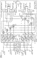
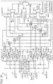
- FIG. 1 is a configuration diagram illustrating a phase detector according to a first embodiment.
- a signal input terminal 1a is a terminal for inputting cos ( ⁇ t) as a first positive-phase signal included in a first differential signal that is a radio frequency signal.
- ⁇ represents an angular frequency
- t represents time.
- a signal input terminal 1b is a terminal for inputting -cos ( ⁇ t) as a first negative-phase signal included in the first differential signal.
- a signal input terminal 1c is a terminal for inputting cos ( ⁇ t + ⁇ ) as a second positive-phase signal included in a second differential signal that is a radio frequency signal.
- a signal input terminal 1d is a terminal for inputting -cos ( ⁇ t + ⁇ ) as a second negative-phase signal included in the second differential signal.
- ⁇ represents a phase difference between the first positive-phase signal cos ( ⁇ t) and the second positive-phase signal cos ( ⁇ t + ⁇ ), and represents a phase difference between the first negative-phase signal -cos ( ⁇ t) and the second negative-phase signal - cos ( ⁇ t + ⁇ ).
- a phase shift circuit 2 includes a phase shifter 2-1, a phase shifter 2-2, a phase shifter 2-3, and a phase shifter 2-4.
- each of the phase shifter 2-1, the phase shifter 2-2, the phase shifter 2-3, and the phase shifter 2-4 is represented by "d".
- the phase shift circuit 2 phase-shifts each of the first positive-phase signal cos ( ⁇ t), the first negative-phase signal -cos ( ⁇ t), the second positive-phase signal cos ( ⁇ t + ⁇ ), and the second negative-phase signal -cos ( ⁇ t + ⁇ ) by a phase shift amount d.
- the phase shift amount d may be stored in an internal memory of the phase shift circuit 2, or may be provided from the outside of the phase detector illustrated in FIG. 1 .
- the phase shift circuit 2 outputs each of a phase-shifted first positive-phase signal cos ( ⁇ t + d), a phase-shifted first negative-phase signal -cos ( ⁇ t + d), a phase-shifted second positive-phase signal cos ( ⁇ t + ⁇ + d), and a phase-shifted second negative-phase signal -cos ( ⁇ t + ⁇ + d) to a multiplication circuit 3 described later.
- An input terminal 2-1a of the phase shifter 2-1 is connected to a signal input terminal 1a, and an output terminal 2-1b of the phase shifter 2-1 is connected to each of an input terminal 3-5b of a fifth multiplier 3-5 described later and an input terminal 3-8b of an eighth multiplier 3-8 described later.
- the phase shifter 2-1 phase-shifts the first positive-phase signal cos ( ⁇ t) by the phase shift amount d, and outputs the phase-shifted first positive-phase signal cos ( ⁇ t + d) to each of the fifth multiplier 3-5 and the eighth multiplier 3-8 from the output terminal 2-1b.
- An input terminal 2-2a of the phase shifter 2-2 is connected to a signal input terminal 1b, and an output terminal 2-2b of the phase shifter 2-2 is connected to each of an input terminal 3-6b of a sixth multiplier 3-6 described later and an input terminal 3-7b of a seventh multiplier 3-7 described later.
- the phase shifter 2-2 phase-shifts the first negative-phase signal -cos ( ⁇ t) by the phase shift amount d, and outputs the phase-shifted first negative-phase signal -cos ( ⁇ t + d) to each of the sixth multiplier 3-6 and the seventh multiplier 3-7 from the output terminal 2-2b.
- An input terminal 2-3a of the phase shifter 2-3 is connected to a signal input terminal 1c, and an output terminal 2-3b of the phase shifter 2-3 is connected to each of an input terminal 3-1b of a first multiplier 3-1 described later and an input terminal 3-4b of a fourth multiplier 3-4 described later.
- the phase shifter 2-3 phase-shifts the second positive-phase signal cos ( ⁇ t + ⁇ ) by the phase shift amount d, and outputs the phase-shifted second positive-phase signal cos ( ⁇ t + ⁇ +d) to each of the first multiplier 3-1 and the fourth multiplier 3-4 from the output terminal 2-3b.
- An input terminal 2-4a of the phase shifter 2-4 is connected to a signal input terminal 1d, and an output terminal 2-4b of the phase shifter 2-4 is connected to each of an input terminal 3-2b of a second multiplier 3-2 described later and an input terminal 3-3b of a third multiplier 3-3 described later.
- the phase shifter 2-4 phase-shifts the second negative-phase signal -cos ( ⁇ t + ⁇ ) by the phase shift amount d, and outputs the phase-shifted second negative-phase signal -cos ( ⁇ t + ⁇ + d) to each of the second multiplier 3-2 and the third multiplier 3-3 from the output terminal 2-4b.
- the multiplication circuit 3 includes the first multiplier 3-1, the second multiplier 3-2, the third multiplier 3-3, the fourth multiplier 3-4, the fifth multiplier 3-5, the sixth multiplier 3-6, the seventh multiplier 3-7, and the eighth multiplier 3-8.
- each of the first multiplier 3-1, the second multiplier 3-2, the third multiplier 3-3, the fourth multiplier 3-4, the fifth multiplier 3-5, the sixth multiplier 3-6, the seventh multiplier 3-7, and the eighth multiplier 3-8 is represented by " ⁇ ".
- the multiplication circuit 3 performs multiplication of two signals for all combinations of the first positive-phase signal cos ( ⁇ t) included in the first differential signal and the first negative-phase signal -cos ( ⁇ t) included in the first differential signal with the second positive-phase signal cos ( ⁇ t + ⁇ + d) phase-shifted by the phase shift circuit 2 and the second negative-phase signal -cos ( ⁇ t + ⁇ + d) phase-shifted by the phase shift circuit 2.
- the multiplication circuit 3 outputs each of cos ( ⁇ t) ⁇ cos ( ⁇ t + ⁇ + d), -cos ( ⁇ t) ⁇ cos ( ⁇ t + ⁇ + d), cos ( ⁇ t) ⁇ cos ( ⁇ t + ⁇ + d), and -cos ( ⁇ t) ⁇ cos ( ⁇ t + ⁇ + d) to a phase difference calculating circuit 4 as a multiplication signal indicating a result of the multiplication.
- the multiplication circuit 3 performs multiplication of two signals for all combinations of the first positive-phase signal cos ( ⁇ t + d) phase-shifted by the phase shift circuit 2 and the first negative-phase signal -cos ( ⁇ t + d) phase-shifted by the phase shift circuit 2, and the second positive-phase signal cos ( ⁇ t + ⁇ ) included in the second differential signal and the second negative-phase signal -cos ( ⁇ t + ⁇ ) included in the second differential signal.
- the multiplication circuit 3 outputs each of cos ( ⁇ t + d) ⁇ cos ( ⁇ t + ⁇ ), -cos ( ⁇ t + d) ⁇ cos ( ⁇ t + ⁇ ), cos ( ⁇ t + d) ⁇ cos ( ⁇ t + ⁇ ), and -cos ( ⁇ t + d) ⁇ cos ( ⁇ t + ⁇ ) to the phase difference calculating circuit 4 as a multiplication signal indicating a result of the multiplication.
- An input terminal 3-1a of the first multiplier 3-1 is connected to the signal input terminal 1a, the input terminal 3-1b of the first multiplier 3-1 is connected to the output terminal 2-3b of the phase shifter 2-3, and an output terminal 3-1c of the first multiplier 3-1 is connected to a two-way divider 5-1 described later.
- the first positive-phase signal cos ( ⁇ t) input from the signal input terminal 1a is input to the input terminal 3-1a of the first multiplier 3-1.
- phase-shifted second positive-phase signal cos ( ⁇ t + ⁇ + d) output from the phase shifter 2-3 is input to the input terminal 3-1b of the first multiplier 3-1.
- the first multiplier 3-1 multiplies the first positive-phase signal cos ( ⁇ t) by the phase-shifted second positive-phase signal cos ( ⁇ t + ⁇ + d), and outputs a first multiplication signal cos ( ⁇ t) ⁇ cos ( ⁇ t + ⁇ + d) indicating a result of the multiplication to the two-way divider 5-1.
- An input terminal 3-2a of the second multiplier 3-2 is connected to the signal input terminal 1a, the input terminal 3-2b of the second multiplier 3-2 is connected to the output terminal 2-4b of the phase shifter 2-4, and an output terminal 3-2c of the second multiplier 3-2 is connected to a two-way divider 5-2 described later.
- the first positive-phase signal cos ( ⁇ t) input from the signal input terminal 1a is input to the input terminal 3-2a of the second multiplier 3-2.
- phase-shifted second negative-phase signal -cos ( ⁇ t + ⁇ + d) output from the phase shifter 2-4 is input to the input terminal 3-2b of the second multiplier 3-2.
- the second multiplier 3-2 multiplies the first positive-phase signal cos ( ⁇ t) by the phase-shifted second negative-phase signal -cos ( ⁇ t + ⁇ + d), and outputs a second multiplication signal -cos ( ⁇ t) ⁇ cos ( ⁇ t + ⁇ + d) indicating a result of the multiplication to the two-way divider 5-2.
- An input terminal 3-3a of the third multiplier 3-3 is connected to the signal input terminal 1b, the input terminal 3-3b of the third multiplier 3-3 is connected to the output terminal 2-4b of the phase shifter 2-4, and an output terminal 3-3c of the third multiplier 3-3 is connected to a two-way divider 5-3 described later.
- the first negative-phase signal -cos ( ⁇ t) input from the signal input terminal 1b is input to the input terminal 3-3a of the third multiplier 3-3.
- phase-shifted second second negative-phase signal -cos ( ⁇ t + ⁇ + d) output from the phase shifter 2-4 is input to the input terminal 3-3b of the third multiplier 3-3.
- the third multiplier 3-3 multiplies the first negative-phase signal -cos ( ⁇ t) by the phase-shifted second negative-phase signal -cos ( ⁇ t + ⁇ + d), and outputs a third multiplication signal cos ( ⁇ t) ⁇ cos ( ⁇ t + ⁇ + d) indicating a result of the multiplication to the two-way divider 5-3.
- An input terminal 3-4a of the fourth multiplier 3-4 is connected to the signal input terminal 1b, the input terminal 3-4b of the fourth multiplier 3-4 is connected to the output terminal 2-3b of the phase shifter 2-3, and an output terminal 3-4c of the fourth multiplier 3-4 is connected to a two-way divider 5-4 described later.
- the first negative-phase signal -cos ( ⁇ t) input from the signal input terminal 1b is input to the input terminal 3-4a of the fourth multiplier 3-4.
- phase-shifted second positive-phase signal cos ( ⁇ t + ⁇ + d) output from the phase shifter 2-3 is input to the input terminal 3-4b of the fourth multiplier 3-4.
- the fourth multiplier 3-4 multiplies the first negative-phase signal -cos ( ⁇ t) by the phase-shifted second positive-phase signal cos ( ⁇ t + ⁇ + d), and outputs a fourth multiplication signal -cos ( ⁇ t) ⁇ cos ( ⁇ t + ⁇ + d) indicating a result of the multiplication to the two-way divider 5-4.
- An input terminal 3-5a of the fifth multiplier 3-5 is connected to the signal input terminal 1c, the input terminal 3-5b of the fifth multiplier 3-5 is connected to the output terminal 2-1b of the phase shifter 2-1, and an output terminal 3-5c of the fifth multiplier 3-5 is connected to a two-way divider 5-5 described later.
- the second positive-phase signal cos ( ⁇ t + ⁇ ) input from the signal input terminal 1c is input to the input terminal 3-5a of the fifth multiplier 3-5.
- phase-shifted first positive-phase signal cos ( ⁇ t + d) output from the phase shifter 2-1 is input to the input terminal 3-5b of the fifth multiplier 3-5.
- the fifth multiplier 3-5 multiplies the second positive-phase signal cos ( ⁇ t + ⁇ ) by the phase-shifted first positive-phase signal cos ( ⁇ t + d), and outputs a fifth multiplication signal cos ( ⁇ t + d) ⁇ cos ( ⁇ t + ⁇ ) indicating a result of the multiplication to the two-way divider 5-5.
- An input terminal 3-6a of the sixth multiplier 3-6 is connected to the signal input terminal 1c, the input terminal 3-6b of the sixth multiplier 3-6 is connected to the output terminal 2-2b of the phase shifter 2-2, and an output terminal 3-6c of the sixth multiplier 3-6 is connected to a two-way divider 5-6 described later.
- the second positive-phase signal cos ( ⁇ t + ⁇ ) input from the signal input terminal 1c is input to the input terminal 3-6a of the sixth multiplier 3-6.
- phase-shifted first negative-phase signal -cos ( ⁇ t + d) output from the phase shifter 2-2 is input to the input terminal 3-6b of the sixth multiplier 3-6.
- the sixth multiplier 3-6 multiplies the second positive-phase signal cos ( ⁇ t + ⁇ ) by the phase-shifted first negative-phase signal -cos ( ⁇ t + d), and outputs a sixth multiplication signal -cos ( ⁇ t + d) ⁇ cos ( ⁇ t + ⁇ ) indicating a result of the multiplication to the two-way divider 5-6.
- An input terminal 3-7a of the seventh multiplier 3-7 is connected to the signal input terminal 1d, the input terminal 3-7b of the seventh multiplier 3-7 is connected to the output terminal 2-2b of the phase shifter 2-2, and an output terminal 3-7c of the seventh multiplier 3-7 is connected to a two-way divider 5-7 described later.
- the second negative-phase signal -cos ( ⁇ t + ⁇ ) input from the signal input terminal 1d is input to the input terminal 3-7a of the seventh multiplier 3-7.
- phase-shifted first negative-phase signal -cos ( ⁇ t + d) output from the phase shifter 2-2 is input to the input terminal 3-7b of the seventh multiplier 3-7.
- the seventh multiplier 3-7 multiplies the second negative-phase signal -cos ( ⁇ t + ⁇ ) by the phase-shifted first negative-phase signal -cos ( ⁇ t + d), and outputs a seventh multiplication signal cos ( ⁇ t + d) ⁇ cos ( ⁇ t + ⁇ ) indicating a result of the multiplication to the two-way divider 5-7.
- An input terminal 3-8a of the eighth multiplier 3-8 is connected to the signal input terminal 1d, the input terminal 3-8b of the eighth multiplier 3-8 is connected to the output terminal 2-1b of the phase shifter 2-1, and an output terminal 3-8c of the eighth multiplier 3-8 is connected to a two-way divider 5-8 described later.
- the second negative-phase signal -cos ( ⁇ t + ⁇ ) input from the signal input terminal 1d is input to the input terminal 3-8a of the eighth multiplier 3-8.
- phase-shifted first positive-phase signal cos ( ⁇ t + d) output from the phase shifter 2-1 is input to the input terminal 3-8b of the eighth multiplier 3-8.
- the eighth multiplier 3-8 multiplies the second negative-phase signal -cos ( ⁇ t + ⁇ ) by the phase-shifted first positive-phase signal cos ( ⁇ t + d), and outputs an eighth multiplication signal -cos ( ⁇ t + d) ⁇ cos ( ⁇ t + ⁇ ) indicating a result of the multiplication to the two-way divider 5-8.
- the phase difference calculating circuit 4 includes the two-way dividers 5-1 to 5-8, a first addition circuit 6-1, a second addition circuit 6-2, a third addition circuit 6-3, a fourth addition circuit 6-4, a first subtraction circuit 7-1, a second subtraction circuit 7-2, a filter 8, a calculation processing circuit 9, and a signal output terminal 10.
- each of the two-way dividers 5-1 to 5-8 is represented by "DIV"
- each of the first addition circuit 6-1, the second addition circuit 6-2, the third addition circuit 6-3, and the fourth addition circuit 6-4 is represented by "+”.
- the phase difference calculating circuit 4 calculates a phase difference ⁇ between a first differential signal and a second differential signal using all multiplication signals output from the multiplication circuit 3.
- the two-way divider 5-1 outputs the first multiplication signal cos ( ⁇ t) ⁇ cos ( ⁇ t + ⁇ + d) output from the first multiplier 3-1 to the first addition circuit 6-1.
- the two-way divider 5-1 outputs the first multiplication signal cos ( ⁇ t) ⁇ cos ( ⁇ t + ⁇ + d) output from the first multiplier 3-1 to the third addition circuit 6-3.
- the two-way divider 5-2 outputs the second multiplication signal -cos ( ⁇ t) ⁇ cos ( ⁇ t + ⁇ + d) output from the second multiplier 3-2 to the second addition circuit 6-2.
- the two-way divider 5-2 outputs the second multiplication signal - cos ( ⁇ t) ⁇ cos ( ⁇ t + ⁇ + d) output from the second multiplier 3-2 to the fourth addition circuit 6-4.
- the two-way divider 5-3 outputs the third multiplication signal cos ( ⁇ t) ⁇ cos ( ⁇ t + ⁇ + d) output from the third multiplier 3-3 to the first addition circuit 6-1.
- the two-way divider 5-3 outputs the third multiplication signal cos ( ⁇ t) ⁇ cos ( ⁇ t + ⁇ + d) output from the third multiplier 3-3 to the third addition circuit 6-3.
- the two-way divider 5-4 outputs the fourth multiplication signal -cos ( ⁇ t) ⁇ cos ( ⁇ t + ⁇ + d) output from the fourth multiplier 3-4 to the second addition circuit 6-2.
- the two-way divider 5-4 outputs the fourth multiplication signal - cos ( ⁇ t) ⁇ cos ( ⁇ t + ⁇ + d) output from the fourth multiplier 3-4 to the fourth addition circuit 6-4.
- the two-way divider 5-5 outputs the fifth multiplication signal cos ( ⁇ t + d) ⁇ cos ( ⁇ t + ⁇ ) output from the fifth multiplier 3-5 to the first addition circuit 6-1.
- the two-way divider 5-5 outputs the fifth multiplication signal cos ( ⁇ t + d) ⁇ cos ( ⁇ t + ⁇ ) output from the fifth multiplier 3-5 to the fourth addition circuit 6-4.
- the two-way divider 5-6 outputs the sixth multiplication signal -cos ( ⁇ t + d) ⁇ cos ( ⁇ t + ⁇ ) output from the sixth multiplier 3-6 to the second addition circuit 6-2.
- the two-way divider 5-6 outputs the sixth multiplication signal -cos ( ⁇ t + d) ⁇ cos ( ⁇ t + ⁇ ) output from the sixth multiplier 3-6 to the third addition circuit 6-3.
- the two-way divider 5-7 outputs the seventh multiplication signal cos ( ⁇ t + d) ⁇ cos ( ⁇ t + ⁇ ) output from the seventh multiplier 3-7 to the first addition circuit 6-1.
- the two-way divider 5-7 outputs the seventh multiplication signal cos ( ⁇ t + d) ⁇ cos ( ⁇ t + ⁇ ) output from the seventh multiplier 3-7 to the fourth addition circuit 6-4.
- the two-way divider 5-8 outputs the eighth multiplication signal -cos ( ⁇ t + d) ⁇ cos ( ⁇ t + ⁇ ) output from the eighth multiplier 3-8 to the second addition circuit 6-2.
- the two-way divider 5-8 outputs the eighth multiplication signal - cos ( ⁇ t + d) ⁇ cos ( ⁇ t + ⁇ ) output from the eighth multiplier 3-8 to the third addition circuit 6-3.
- the first addition circuit 6-1 adds the first multiplication signal cos ( ⁇ t) ⁇ cos ( ⁇ t + ⁇ + d) output from the two-way divider 5-1, the third multiplication signal cos ( ⁇ t) ⁇ cos ( ⁇ t + ⁇ + d) output from the two-way divider 5-3, the fifth multiplication signal cos ( ⁇ t + d) ⁇ cos ( ⁇ t + ⁇ ) output from the two-way divider 5-5, and the seventh multiplication signal cos ( ⁇ t + d) ⁇ cos ( ⁇ t + ⁇ ) output from the two-way divider 5-7.
- the first addition circuit 6-1 outputs a first addition signal 2•cos (2 ⁇ t + ⁇ + d) + cos ( ⁇ + d) + cos ( ⁇ - d) indicating a result of the addition to the first subtraction circuit 7-1.
- the second addition circuit 6-2 adds the second multiplication signal -cos ( ⁇ t) ⁇ cos ( ⁇ t + ⁇ + d) output from the two-way divider 5-2, the fourth multiplication signal -cos ( ⁇ t) ⁇ cos ( ⁇ t + ⁇ + d) output from the two-way divider 5-4, the sixth multiplication signal -cos ( ⁇ t + d) ⁇ cos ( ⁇ t + ⁇ ) output from the two-way divider 5-6, and the eighth multiplication signal -cos ( ⁇ t + d) ⁇ cos ( ⁇ t + ⁇ ) output from the two-way divider 5-8.
- the second addition circuit 6-2 outputs a second addition signal -2•cos (2 ⁇ t + ⁇ + d) + cos ( ⁇ + d) + cos ( ⁇ - d) indicating a result of the addition to the first subtraction circuit 7-1.
- the third addition circuit 6-3 adds the first multiplication signal cos ( ⁇ t) ⁇ cos ( ⁇ t + ⁇ + d) output from the two-way divider 5-1, the third multiplication signal cos ( ⁇ t) ⁇ cos ( ⁇ t + ⁇ + d) output from the two-way divider 5-3, the sixth multiplication signal -cos ( ⁇ t + d) ⁇ cos ( ⁇ t + ⁇ ) output from the two-way divider 5-6, and the eighth multiplication signal -cos ( ⁇ t + d) ⁇ cos ( ⁇ t + ⁇ ) output from the two-way divider 5-8.
- the third addition circuit 6-3 outputs a third addition signal -4•sin ( ⁇ ) sin (d) indicating a result of the addition to the second subtraction circuit 7-2.
- the fourth addition circuit 6-4 adds the second multiplication signal -cos ( ⁇ t) ⁇ cos ( ⁇ t + ⁇ + d) output from the two-way divider 5-2, the fourth multiplication signal - cos ( ⁇ t) ⁇ cos ( ⁇ t + ⁇ + d) output from the two-way divider 5-4, the fifth multiplication signal cos ( ⁇ t + d) ⁇ cos ( ⁇ t + ⁇ ) output from the two-way divider 5-5, and the seventh multiplication signal cos ( ⁇ t + d) ⁇ cos ( ⁇ t + ⁇ ) output from the two-way divider 5-7.
- the fourth addition circuit 6-4 outputs a fourth addition signal 4•sin ( ⁇ ) sin (d) indicating a result of the addition to the second subtraction circuit 7-2.
- the first subtraction circuit 7-1 subtracts the second addition signal -2•cos (2 ⁇ t + ⁇ + d) + cos ( ⁇ + d) + cos ( ⁇ - d) output from the second addition circuit 6-2 from the first addition signal 2•cos (2 ⁇ t + ⁇ + d) + cos ( ⁇ + d) + cos ( ⁇ - d) output from the first addition circuit 6-1.
- the first subtraction circuit 7-1 outputs a first subtraction signal 4•cos (2 ⁇ t + ⁇ + d) indicating a result of the subtraction to the filter 8.
- the second subtraction circuit 7-2 subtracts the third addition signal -4•sin ( ⁇ ) sin (d) output from the third addition circuit 6-3 from the fourth addition signal 4•sin ( ⁇ ) sin (d) output from the fourth addition circuit 6-4.
- the second subtraction circuit 7-2 outputs a second subtraction signal 8•sin ( ⁇ ) sin (d) indicating a result of the subtraction to the calculation processing circuit 9.
- the filter 8 is implemented by, for example, a low pass filter (LPF) or a band ppass filter (BPF).
- LPF low pass filter
- BPF band ppass filter
- the filter 8 removes a high-frequency component included in the first subtraction signal 4•cos (2 ⁇ t + ⁇ + d) output from the first subtraction circuit 7-1.
- the filter 8 outputs the first subtraction signal 8•cos ( ⁇ ) cos (d) after removal of the high-frequency component to the calculation processing circuit 9.
- the calculation processing circuit 9 calculates a phase difference ⁇ between a first differential signal and a second differential signal from the first subtraction signal 8•cos ( ⁇ ) cos (d) after removal of the high-frequency component output from the filter 8 and the second subtraction signal 8•sin ( ⁇ ) sin (d) output from the second subtraction circuit 7-2.
- the calculation processing circuit 9 outputs the calculated phase difference ⁇ to the signal output terminal 10.
- the signal output terminal 10 is a terminal for outputting the phase difference ⁇ calculated by the calculation processing circuit 9 to the outside.
- the phase detector illustrated in FIG. 1 calculates a phase difference ⁇ between a first differential signal and a second differential signal.
- the first positive-phase signal cos ( ⁇ t) included in the first differential signal is input from the signal input terminal 1a, and the first negative-phase signal -cos ( ⁇ t) included in the first differential signal is input from the signal input terminal 1b.
- the second positive-phase signal cos ( ⁇ t + ⁇ ) included in the second differential signal is input from the signal input terminal 1c, and the second negative-phase signal -cos ( ⁇ t + ⁇ ) included in the second differential signal is input from the signal input terminal 1d.
- phase shifter 2-1 When the first positive-phase signal cos ( ⁇ t) input from the signal input terminal 1a is input from the input terminal 2-1a to the phase shifter 2-1, the phase shifter 2-1 phase-shifts the first positive-phase signal cos ( ⁇ t) by a phase shift amount d.
- the phase shifter 2-1 outputs the phase-shifted first positive-phase signal cos ( ⁇ t + d) from the output terminal 2-1b to each of the fifth multiplier 3-5 and the eighth multiplier 3-8.
- the phase shifter 2-2 phase-shifts the first negative-phase signal -cos ( ⁇ t) by the phase shift amount d.
- the phase shifter 2-2 outputs the phase-shifted first negative-phase signal -cos ( ⁇ t + d) from the output terminal 2-2b to each of the sixth multiplier 3-6 and the seventh multiplier 3-7.
- phase shifter 2-3 phase-shifts the second positive-phase signal cos ( ⁇ t + ⁇ ) by the phase shift amount d.
- the phase shifter 2-3 outputs the phase-shifted second positive-phase signal cos ( ⁇ t + ⁇ + d) from the output terminal 2-3b to each of the first multiplier 3-1 and the fourth multiplier 3-4.
- phase shifter 2-4 phase-shifts the second negative-phase signal -cos ( ⁇ t + ⁇ ) by the phase shift amount d.
- the phase shifter 2-4 outputs the phase-shifted second negative-phase signal - cos ( ⁇ t + ⁇ + d) from the output terminal 2-4b to each of the second multiplier 3-2 and the third multiplier 3-3.
- the first positive-phase signal cos ( ⁇ t) input from the signal input terminal 1a is input to the input terminal 3-1a of the first multiplier 3-1, and the phase-shifted second positive-phase signal cos ( ⁇ t + ⁇ + d) output from the phase shifter 2-3 is input to the input terminal 3-1b.
- the first multiplier 3-1 multiplies the first positive-phase signal cos ( ⁇ t) by the phase-shifted second positive-phase signal cos ( ⁇ t + ⁇ + d).
- the first multiplier 3-1 outputs a first multiplication signal cos ( ⁇ t) ⁇ cos ( ⁇ t + ⁇ + d) indicating a result of the multiplication to the two-way divider 5-1.
- the first positive-phase signal cos ( ⁇ t) input from the signal input terminal 1a is input to the input terminal 3-2a of the second multiplier 3-2, and the phase-shifted second negative-phase signal -cos ( ⁇ t + ⁇ + d) output from the phase shifter 2-4 is input to the input terminal 3-2b.
- the second multiplier 3-2 multiplies the first positive-phase signal cos ( ⁇ t) by the phase-shifted second negative-phase signal -cos ( ⁇ t + ⁇ + d).
- the second multiplier 3-2 outputs a second multiplication signal -cos ( ⁇ t) ⁇ cos ( ⁇ t + ⁇ + d) indicating a result of the multiplication to the two-way divider 5-2.
- the first negative-phase signal -cos ( ⁇ t) input from the signal input terminal 1b is input to the input terminal 3-3a of the third multiplier 3-3, and the phase-shifted second second negative-phase signal -cos ( ⁇ t + ⁇ + d) output from the phase shifter 2-4 is input to the input terminal 3-3b.
- the third multiplier 3-3 multiplies the first negative-phase signal -cos ( ⁇ t) by the phase-shifted second negative-phase signal -cos ( ⁇ t + ⁇ + d).
- the third multiplier 3-3 outputs a third multiplication signal cos ( ⁇ t) ⁇ cos ( ⁇ t + ⁇ + d) indicating a result of the multiplication to the two-way divider 5-3.
- the first negative-phase signal -cos ( ⁇ t) input from the signal input terminal 1b is input to the input terminal 3-4a of the fourth multiplier 3-4, and the phase-shifted second positive-phase signal cos ( ⁇ t + ⁇ + d) output from the phase shifter 2-3 is input to the input terminal 3-4b.
- the fourth multiplier 3-4 multiplies the first negative-phase signal -cos ( ⁇ t) by the phase-shifted second positive-phase signal cos ( ⁇ t + ⁇ + d).
- the fourth multiplier 3-4 outputs a fourth multiplication signal -cos ( ⁇ t) ⁇ cos ( ⁇ t + ⁇ + d) indicating a result of the multiplication to the two-way divider 5-4.
- the second positive-phase signal cos ( ⁇ t + ⁇ ) input from the signal input terminal 1c is input to the input terminal 3-5a of the fifth multiplier 3-5, and the phase-shifted first positive-phase signal cos ( ⁇ t + d) output from the phase shifter 2-1 is input to the input terminal 3-5b.
- the fifth multiplier 3-5 multiplies the second positive-phase signal cos ( ⁇ t + ⁇ ) by the phase-shifted first positive-phase signal cos ( ⁇ t + d).
- the fifth multiplier 3-5 outputs a fifth multiplication signal cos ( ⁇ t + d) ⁇ cos ( ⁇ t + ⁇ ) indicating a result of the multiplication to the two-way divider 5-5.
- the second positive-phase signal cos ( ⁇ t + ⁇ ) input from the signal input terminal 1c is input to the input terminal 3-6a of the sixth multiplier 3-6, and the phase-shifted first negative-phase signal -cos ( ⁇ t + d) output from the phase shifter 2-2 is input to the input terminal 3-6b.
- the sixth multiplier 3-6 multiplies the second positive-phase signal cos ( ⁇ t + ⁇ ) by the phase-shifted first negative-phase signal -cos ( ⁇ t + d).
- the sixth multiplier 3-6 outputs a sixth multiplication signal -cos ( ⁇ t + d) ⁇ cos ( ⁇ t + ⁇ ) indicating a result of the multiplication to the two-way divider 5-6.
- the second negative-phase signal -cos ( ⁇ t + ⁇ ) input from the signal input terminal 1d is input to the input terminal 3-7a of the seventh multiplier 3-7, and the phase-shifted first negative-phase signal -cos ( ⁇ t + d) output from the phase shifter 2-2 is input to the input terminal 3-7b.
- the seventh multiplier 3-7 multiplies the second negative-phase signal -cos ( ⁇ t + ⁇ ) by the phase-shifted first negative-phase signal -cos ( ⁇ t + d).
- the seventh multiplier 3-7 outputs a seventh multiplication signal cos ( ⁇ t + d) ⁇ cos ( ⁇ t + ⁇ ) indicating a result of the multiplication to the two-way divider 5-7.
- the second negative-phase signal -cos ( ⁇ t + ⁇ ) input from the signal input terminal Id is input to the input terminal 3-8a of the eighth multiplier 3-8, and the phase-shifted first positive-phase signal cos ( ⁇ t + d) output from the phase shifter 2-1 is input to the input terminal 3-8b.
- the eighth multiplier 3-8 multiplies the second negative-phase signal -cos ( ⁇ t + ⁇ ) by the phase-shifted first positive-phase signal cos ( ⁇ t + d).
- the eighth multiplier 3-8 outputs an eighth multiplication signal -cos ( ⁇ t + d) ⁇ cos ( ⁇ t + ⁇ ) indicating a result of the multiplication to the two-way divider 5-8.
- the two-way divider 5-1 When receiving the first multiplication signal cos ( ⁇ t) ⁇ cos ( ⁇ t + ⁇ + d) from the first multiplier 3-1, the two-way divider 5-1 outputs the first multiplication signal cos ( ⁇ t) ⁇ cos ( ⁇ t + ⁇ + d) to each of the first addition circuit 6-1 and the third addition circuit 6-3.
- the two-way divider 5-2 When receiving the second multiplication signal -cos ( ⁇ t) ⁇ cos ( ⁇ t + ⁇ + d) from the second multiplier 3-2, the two-way divider 5-2 outputs the second multiplication signal -cos ( ⁇ t) ⁇ cos ( ⁇ t + ⁇ + d) to each of the second addition circuit 6-2 and the fourth addition circuit 6-4.
- the two-way divider 5-3 When receiving the third multiplication signal cos ( ⁇ t) ⁇ cos ( ⁇ t + ⁇ + d) from the third multiplier 3-3, the two-way divider 5-3 outputs the third multiplication signal cos ( ⁇ t) ⁇ cos ( ⁇ t + ⁇ + d) to each of the first addition circuit 6-1 and the third addition circuit 6-3.
- the two-way divider 5-4 When receiving the fourth multiplication signal -cos ( ⁇ t) ⁇ cos ( ⁇ t + ⁇ + d) from the fourth multiplier 3-4, the two-way divider 5-4 outputs the fourth multiplication signal -cos ( ⁇ t) ⁇ cos ( ⁇ t + ⁇ + d) to each of the second addition circuit 6-2 and the fourth addition circuit 6-4.
- the two-way divider 5-5 When receiving the fifth multiplication signal cos ( ⁇ t + d) ⁇ cos ( ⁇ t + ⁇ ) from the fifth multiplier 3-5, the two-way divider 5-5 outputs the fifth multiplication signal cos ( ⁇ t + d) ⁇ cos ( ⁇ t + ⁇ ) to each of the first addition circuit 6-1 and the fourth addition circuit 6-4.
- the two-way divider 5-6 When receiving the sixth multiplication signal -cos ( ⁇ t + d) ⁇ cos ( ⁇ t + ⁇ ) from the sixth multiplier 3-6, the two-way divider 5-6 outputs the sixth multiplication signal -cos ( ⁇ t + d) ⁇ cos ( ⁇ t + ⁇ ) to each of the second addition circuit 6-2 and the third addition circuit 6-3.
- the two-way divider 5-7 When receiving the seventh multiplication signal cos ( ⁇ t + d) ⁇ cos ( ⁇ t + ⁇ ) from the seventh multiplier 3-7, the two-way divider 5-7 outputs the seventh multiplication signal cos ( ⁇ t + d) ⁇ cos ( ⁇ t + ⁇ ) to each of the first addition circuit 6-1 and the fourth addition circuit 6-4.
- the two-way divider 5-8 When receiving the eighth multiplication signal -cos ( ⁇ t + d) ⁇ cos ( ⁇ t + ⁇ ) from the eighth multiplier 3-8, the two-way divider 5-8 outputs the eighth multiplication signal -cos ( ⁇ t + d) ⁇ cos ( ⁇ t + ⁇ ) to each of the second addition circuit 6-2 and the third addition circuit 6-3.
- the first addition circuit 6-1 adds the first multiplication signal cos ( ⁇ t) ⁇ cos ( ⁇ t + ⁇ + d), the third multiplication signal cos ( ⁇ t) ⁇ cos ( ⁇ t + ⁇ + d), the fifth multiplication signal cos ( ⁇ t + d) ⁇ cos ( ⁇ t + ⁇ ), and the seventh multiplication signal cos ( ⁇ t + d) ⁇ cos ( ⁇ t + ⁇ ).
- the first addition circuit 6-1 outputs a first addition signal 2•cos (2 ⁇ t + ⁇ + d) + cos ( ⁇ + d) + cos ( ⁇ - d) indicating a result of the addition to the first subtraction circuit 7-1.
- the second addition circuit 6-2 adds the second multiplication signal -cos ( ⁇ t) ⁇ cos ( ⁇ t + ⁇ + d), the fourth multiplication signal -cos ( ⁇ t) ⁇ cos ( ⁇ t + ⁇ + d), the sixth multiplication signal -cos ( ⁇ t + d) ⁇ cos ( ⁇ t + ⁇ ), and the eighth multiplication signal - cos ( ⁇ t + d) ⁇ cos ( ⁇ t + ⁇ ).
- the second addition circuit 6-2 outputs a second addition signal -2•cos (2 ⁇ t + ⁇ + d) + cos ( ⁇ + d) + cos ( ⁇ - d) indicating a result of the addition to the first subtraction circuit 7-1.
- the third addition circuit 6-3 adds the first multiplication signal cos ( ⁇ t) ⁇ cos ( ⁇ t + ⁇ + d), the third multiplication signal cos ( ⁇ t) ⁇ cos ( ⁇ t + ⁇ + d), the sixth multiplication signal -cos ( ⁇ t + d) ⁇ cos ( ⁇ t + ⁇ ), and the eighth multiplication signal - cos ( ⁇ t + d) ⁇ cos ( ⁇ t + ⁇ ).
- the third addition circuit 6-3 outputs a third addition signal -4•sin ( ⁇ ) sin (d) indicating a result of the addition to the second subtraction circuit 7-2.
- the fourth addition circuit 6-4 adds the second multiplication signal -cos ( ⁇ t) ⁇ cos ( ⁇ t + ⁇ + d), the fourth multiplication signal -cos ( ⁇ t) ⁇ cos ( ⁇ t + ⁇ + d), the fifth multiplication signal cos ( ⁇ t + d) ⁇ cos ( ⁇ t + ⁇ ), and the seventh multiplication signal cos ( ⁇ t + d) ⁇ cos ( ⁇ t + ⁇ ).
- the fourth addition circuit 6-4 outputs a fourth addition signal 4•sin ( ⁇ ) sin (d) indicating a result of the addition to the second subtraction circuit 7-2.
- the first addition signal 2•cos (2 ⁇ t + ⁇ + d) + cos ( ⁇ + d) + cos ( ⁇ - d) output from the first addition circuit 6-1 and the second addition signal -2•cos (2 ⁇ t + ⁇ + d) + cos ( ⁇ + d) + cos ( ⁇ - d) output from the second addition circuit 6-2 are input.
- the first subtraction circuit 7-1 subtracts the second addition signal -2•cos (2 ⁇ t + ⁇ + d) + cos ( ⁇ + d) + cos ( ⁇ - d) from the first addition signal 2•cos (2 ⁇ t + ⁇ + d) + cos ( ⁇ + d) + cos ( ⁇ - d).
- the first subtraction circuit 7-1 outputs a first subtraction signal 4•cos (2 ⁇ t + ⁇ + d) indicating a result of the subtraction to the filter 8.
- the fourth addition signal 4•sin ( ⁇ ) sin (d) output from the fourth addition circuit 6-4 and the third addition signal -4•sin ( ⁇ ) sin (d) output from the third addition circuit 6-3 are input.
- the second subtraction circuit 7-2 subtracts the third addition signal -4•sin ( ⁇ ) sin (d) from the fourth addition signal 4•sin ( ⁇ ) sin (d).
- the second subtraction circuit 7-2 outputs a second subtraction signal 8•sin ( ⁇ ) sin (d) indicating a result of the subtraction to the calculation processing circuit 9.
- the filter 8 When receiving the first subtraction signal 4•cos (2 ⁇ t + ⁇ + d) from the first subtraction circuit 7-1, the filter 8 removes a high-frequency component included in the first subtraction signal 4•cos (2 ⁇ t + ⁇ + d).
- the high-frequency component included in the first subtraction signal 4•cos (2 ⁇ t + ⁇ + d) is a component other than a DC component included in the first subtraction signal 4•cos (2 ⁇ t + ⁇ + d).
- the filter 8 outputs the first subtraction signal 8•cos ( ⁇ ) cos (d) after removal of the high-frequency component to the calculation processing circuit 9.
- the first subtraction signal 8•cos ( ⁇ ) cos (d) after removal of the high-frequency component output from the filter 8 and the second subtraction signal 8•sin ( ⁇ ) sin (d) output from the second subtraction circuit 7-2 are input.
- the calculation processing circuit 9 calculates a phase difference ⁇ between a first differential signal and a second differential signal from the first subtraction signal 8•cos ( ⁇ ) cos (d) after removal of the high-frequency component and the second subtraction signal 8•sin ( ⁇ ) sin (d) as indicated in the following formula (1).
- ⁇ tan ⁇ 1 8 ⁇ sin ⁇ sin d 8 ⁇ cos ⁇ cos d ⁇ cos d sin d
- each of cos (d) and sin (d) is also a predetermined value.
- each of cos (d) and sin (d) may be stored in an internal memory of the calculation processing circuit 9, or may be provided from the outside of the phase detector illustrated in FIG. 1 .
- the calculation processing circuit 9 outputs the calculated phase difference ⁇ to the signal output terminal 10.
- phase difference ⁇ between a first differential signal and a second differential signal can be calculated.
- the phase shift amount d in which cos (d) or sin (d) is not zero is a phase shift amount other than 0 degrees, 90 degrees, 180 degrees, or 270 degrees.
- a range in which the phase difference ⁇ can be detected is not limited to a range of 180 degrees.
- the phase shift amount is d.
- the first subtraction signal after removal of the high-frequency component output from the filter 8 is 8•cos ( ⁇ ) cos (45).
- the second subtraction signal output from the second subtraction circuit 7-2 is 8•sin ( ⁇ ) sin (45).
- phase difference ⁇ calculated by the calculation processing circuit 9 is represented by the following formula (2).
- ⁇ tan ⁇ 1 8 ⁇ sin ⁇ sin 45 8 ⁇ cos ⁇ cos 45 ⁇ cos 45
- sin 45 tan ⁇ 1 8 ⁇ sin ⁇ sin 45 8 ⁇ cos ⁇ cos 45
- the calculation processing circuit 9 does not need to multiply the term cos (d)/sin (d) as indicated by formula (2), and therefore the circuit of the calculation processing circuit 9 can be simplified as compared with a case of d ⁇ 45 degrees.
- the phase detector includes: the phase shift circuit 2 to phase-shift each of a first positive-phase signal included in a first differential signal and a first negative-phase signal included in the first differential signal, and phase-shift each of a second positive-phase signal included in a second differential signal and a second negative-phase signal included in the second differential signal; the multiplication circuit 3 to perform multiplication of two signals for all combinations of the first positive-phase signal included in the first differential signal and the first negative-phase signal included in the first differential signal with the second positive-phase signal phase-shifted by the phase shift circuit 2 and the second negative-phase signal phase-shifted by the phase shift circuit 2, output a multiplication signal indicating a result of the multiplication, perform multiplication of two signals for all combinations of the first positive-phase signal phase-shifted by the phase shift circuit 2 and the first negative-phase signal phase-shifted by the phase shift circuit 2 with the second positive-phase signal included in the second differential signal and the second negative-phase signal included in the second differential signal, and output a multiplication signal indicating a
- each of the phase shifter 2-1, the phase shifter 2-2, the phase shifter 2-3, and the phase shifter 2-4 can be implemented by a distributed constant circuit.
- a phase shift amount d in each of the phase shifter 2-1, the phase shifter 2-2, the phase shifter 2-3, and the phase shifter 2-4 only needs to be a phase shift amount other than 0 degrees, 90 degrees, 180 degrees, or 270 degrees, and may be, for example, a phase shift amount of less than 90 degrees.
- the length of a line included in the distributed constant circuit is represented by the following formula (3) when the frequency of each of a first differential signal and a second differential signal is 1 (GHz).
- 3 ⁇ 10 8 (m/s) is a speed in vacuum, and a speed on a substrate may be slower than 3 ⁇ 10 8 (m/s).
- the width of the line included in the distributed constant circuit is, for example, 10 ( ⁇ m)
- phase shifter 2-1 the phase shifter 2-2, the phase shifter 2-3, and the phase shifter 2-4
- a phase shifter having a phase shift amount d of 90 degrees cannot be used, but if a phase shifter having a phase shift amount d of 90 degrees is used, the length of the line included in the distributed constant circuit is 7.5 (cm).
- the width of the line included in the distributed constant circuit is, for example, 10 ( ⁇ m)
- the area occupied by the line included in the distributed constant circuit is 7500 ( ⁇ m 2 ).
- each of the phase shifter 2-1, the phase shifter 2-2, the phase shifter 2-3, and the phase shifter 2-4 is, for example, a phase shifter having a phase shift amount d of 20 degrees
- the area occupied by the line included in the distributed constant circuit is about half as compared with a case of a phase shifter having a phase shift amount d of 90 degrees.
- each of the phase shifter 2-1, the phase shifter 2-2, the phase shifter 2-3, and the phase shifter 2-4 can be implemented by a lumped constant circuit.
- the phase shifter 2-1, the phase shifter 2-2, the phase shifter 2-3, and the phase shifter 2-4 is implemented by the lumped constant circuit, it is possible to reduce the size as compared with a case where each of the phase shifter 2-1, the phase shifter 2-2, the phase shifter 2-3, and the phase shifter 2-4 is implemented by the distributed constant circuit.
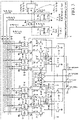
- the phase shifter 2-1 can be implemented by a lumped constant circuit such as a low-pass filter including a resistor 21 and a capacitor 22.
- FIG. 2 is a configuration diagram illustrating an example of the phase shifter 2-1 implemented by the lumped constant circuit.
- Each of the phase shifter 2-2, the phase shifter 2-3, and the phase shifter 2-4 can be configured similarly to the phase shifter 2-1.
- an input terminal 20 is connected to the signal input terminal 1a.
- An output terminal 23 is connected to each of the input terminal 3-5a of the fifth multiplier 3-5 and the input terminal 3-8a of the eighth multiplier 3-8.
- One end of the resistor 21 is connected to the input terminal 20, and the other end of the resistor 21 is connected to each of one end of the capacitor 22 and the output terminal 23.
- One end of the capacitor 22 is connected to each of the other end of the resistor 21 and the output terminal 23, and the other end of the capacitor 22 is grounded.
- a transfer function Z of the phase shifter 2-1 illustrated in FIG. 2 is represented by the following formula (5).
- Z 1 1 + j ⁇ CR
- R represents a resistance value of the resistor 21
- C represents a capacitance value of the capacitor 22.
- of the phase shifter 2-1 illustrated in FIG. 2 is represented by the following formula (6), and a passage phase shift arg (Z) of the phase shifter 2-1 illustrated in FIG. 2 is represented by the following formula (7).
- Z 1 1 + j ⁇ CR arg
- Z ⁇ tan ⁇ 1 ⁇ CR
- at this time is 0.93, indicating a loss of 7%.
- the loss of 7% is 0.5 (dB). Since the loss of 0.5 (dB) of the phase shifter 2-1 illustrated in FIG. 2 is smaller than, for example, a loss of a phase shifter using a polyphase filter, the phase shifter 2-1 illustrated in FIG. 2 can reduce power consumption as compared with the phase shifter using a polyphase filter.
- the phase shifter using a polyphase filter has a passage loss of 6 (dB) in principle.
- a capacitance value C of the capacitor 22 is 1.15 (pF).
- the phase shifter 2-1 is implemented by a 0.18 ( ⁇ m) complementary metal oxide semiconductor (CMOS) process
- the area of the resistor 21 is about 3 ( ⁇ m) ⁇ 2 ( ⁇ m)
- the area of the capacitor 22 is about 30 ( ⁇ m) ⁇ 30 ( ⁇ m). Therefore, the area of the phase shifter 2-1 illustrated in FIG. 2 is about 30 ( ⁇ m 2 ), and the area of the phase shifter 2-1 illustrated in FIG. 2 is smaller than the area of the phase shifter 2-1 when the phase shifter 2-1 is implemented by the distributed constant circuit.
- phase shifters 2-1 to 2-4 which are components of phase shift circuit 2 are the same as each other.
- the configurations of the first multiplier 3-1, the second multiplier 3-2, the third multiplier 3-3, the fourth multiplier 3-4, the fifth multiplier 3-5, the sixth multiplier 3-6, the seventh multiplier 3-7, and the eighth multiplier 3-8, which are components of the multiplication circuit 3, are the same as each other.
- the configurations of the two-way dividers 5-1 to 5-8 which are some components of a phase difference detecting circuit 4, are the same as each other, and the configurations of the first addition circuit 6-1, the second addition circuit 6-2, the third addition circuit 6-3, and the fourth addition circuit 6-4 are the same as each other.
- the configurations of the first subtraction circuit 7-1 and the second subtraction circuit 7-2 are the same as each other.
- the calculation processing circuit 9 calculates a phase difference ⁇ between a first differential signal and a second differential signal on the basis of a ratio between the first subtraction signal 8•cos ( ⁇ ) cos (d) after removal of the high-frequency component and the second subtraction signal 8•sin ( ⁇ ) sin (d) as indicated in formula (1).
- both the first subtraction signal 8•cos ( ⁇ ) cos (d) after removal of the high-frequency component and the second subtraction signal 8•sin ( ⁇ ) sin (d) increase or decrease, an influence on the ratio is small and deterioration in calculation accuracy of the phase difference ⁇ is small as compared with a case where either one of the first subtraction signal 8•cos ( ⁇ ) cos (d) after removal of the high-frequency component and the second subtraction signal 8•sin ( ⁇ ) sin (d) increases or decreases.
- a phase detector in which a multiplication circuit 3 includes transistors 3-1' to 3-8' as a first multiplier 3-1, a second multiplier 3-2, a third multiplier 3-3, a fourth multiplier 3-4, a fifth multiplier 3-5, a sixth multiplier 3-6, a seventh multiplier 3-7, and an eighth multiplier 3-8 will be described.
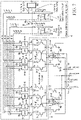
- FIG. 3 is a configuration diagram illustrating the phase detector according to the second embodiment.
- FIG. 3 the same reference numerals as in FIG. 1 indicate the same or corresponding parts, and therefore description thereof is omitted.
- Each of transistors 11-1 to 11-4 is a nonlinear element such as a bipolar transistor.
- a base terminal of the transistor 11-1 is connected to a signal input terminal 1a, and a collector terminal of the transistor 11-1 is connected to an emitter terminal of each of the transistor 3-1' and the transistor 3-2'. In addition, an emitter terminal of the transistor 11-1 is grounded.
- the transistor 11-1 multiplies the amplitude of a first positive-phase signal cos ( ⁇ t) input from the signal input terminal 1a by ⁇ , and outputs the first positive-phase signal acos ( ⁇ t) obtained by multiplying the amplitude by ⁇ to the emitter terminal of each of the transistor 3-1' and the transistor 3-2'.
- ⁇ is a value equal to or more than 1.
- a base terminal of the transistor 11-2 is connected to a signal input terminal 1b, and a collector terminal of the transistor 11-2 is connected to an emitter terminal of each of the transistor 3-3' and the transistor 3-4'. In addition, an emitter terminal of the transistor 11-2 is grounded.
- the transistor 11-2 multiplies the amplitude of a first negative-phase signal - cos ( ⁇ t) input from the signal input terminal 1b by ⁇ , and outputs the first negative-phase signal -acos ( ⁇ t) obtained by multiplying the amplitude by ⁇ to the emitter terminal of each of the transistor 3-3' and the transistor 3-4'.
- a base terminal of the transistor 11-3 is connected to a signal input terminal 1c, and a collector terminal of the transistor 11-3 is connected to an emitter terminal of each of the transistor 3-5' and the transistor 3-6'. In addition, an emitter terminal of the transistor 11-3 is grounded.
- the transistor 11-3 multiplies the amplitude of a second positive-phase signal cos ( ⁇ t + ⁇ ) input from the signal input terminal 1c by ⁇ , and outputs the second positive-phase signal acos ( ⁇ t + ⁇ ) obtained by multiplying the amplitude by ⁇ to the emitter terminal of each of the transistor 3-5' and the transistor 3-6'.
- Abase terminal of the transistor 11-4 is connected to a signal input terminal 1d, and a collector terminal of the transistor 11-4 is connected to an emitter terminal of each of the transistor 3-7' and the transistor 3-8'. In addition, an emitter terminal of the transistor 11-4 is grounded.
- the transistor 11-4 multiplies the amplitude of a second negative-phase signal - cos ( ⁇ t + ⁇ ) input from the signal input terminal 1d by ⁇ , and outputs the second negative-phase signal -acos ( ⁇ t + ⁇ ) obtained by multiplying the amplitude by ⁇ to the emitter terminal of each of the transistor 3-7' and the transistor 3-8'.
- the multiplication circuit 3 includes the transistors 3-1' to 3-8' as the first multiplier 3-1, the second multiplier 3-2, the third multiplier 3-3, the fourth multiplier 3-4, the fifth multiplier 3-5, the sixth multiplier 3-6, the seventh multiplier 3-7, and the eighth multiplier 3-8.
- Each of the transistors 3-1' to 3-8' is a nonlinear element such as a bipolar transistor.
- a base terminal of the transistor 3-1' is connected to each of an output terminal 2-3b of a phase shifter 2-3 and a base terminal of the transistor 3-4', and a collector terminal of the transistor 3-1' is connected to a terminal 5a described later of a two-way divider 5-1.
- an emitter terminal of the transistor 3-1' is connected to each of a collector terminal of the transistor 11-1 and an emitter terminal of the transistor 3-2'.
- the transistor 3-1' multiplies a difference between a phase-shifted second positive-phase signal cos ( ⁇ t + ⁇ + d) output from the phase shifter 2-3 and a first positive-phase signal acos ( ⁇ t) output from the transistor 11-1 by a transconductance g n .
- a current I 1 indicated in the following formula (8) flows from the two-way divider 5-1 to a collector terminal of the transistor 3-1'.
- the current I 1 corresponds to a first multiplication signal cos ( ⁇ t) ⁇ cos ( ⁇ t + ⁇ + d) output from the first multiplier 3-1.
- n represents the order of a harmonic, and n is an integer equal to or more than 2.
- a base terminal of the transistor 3-2' is connected to each of an output terminal 2-4b of a phase shifter 2-4 and a base terminal of the transistor 3-3', and a collector terminal of the transistor 3-2' is connected to a terminal 5a of a two-way divider 5-2.
- an emitter terminal of the transistor 3-2' is connected to each of a collector terminal of the transistor 11-1 and an emitter terminal of the transistor 3-1'.
- the transistor 3-2' multiplies a difference between a phase-shifted second negative-phase signal -cos ( ⁇ t + ⁇ + d) output from the phase shifter 2-4 and a first positive-phase signal acos ( ⁇ t) output from the transistor 11-1 by the transconductance g n .
- a current I 2 indicated in the following formula (9) flows from the two-way divider 5-2 to a collector terminal of the transistor 3-2'.
- the current I 2 corresponds to a second multiplication signal -cos ( ⁇ t) ⁇ cos ( ⁇ t + ⁇ + d) output from the second multiplier 3-2.
- a base terminal of the transistor 3-3' is connected to each of an output terminal 2-4b of the phase shifter 2-4 and a base terminal of the transistor 3-2', and a collector terminal of the transistor 3-3' is connected to a terminal 5a of a two-way divider 5-3.
- an emitter terminal of the transistor 3-3' is connected to each of a collector terminal of the transistor 11-2 and an emitter terminal of the transistor 3-4'.
- the transistor 3-3' multiplies a difference between a phase-shifted second negative-phase signal -cos ( ⁇ t + ⁇ + d) output from the phase shifter 2-4 and a first negative-phase signal -acos ( ⁇ t) output from the transistor 11-2 by the transconductance g n .
- a current I 3 indicated in the following formula (10) flows from the two-way divider 5-3 to a collector terminal of the transistor 3-3'.
- the current I 3 corresponds to a third multiplication signal cos ( ⁇ t) ⁇ cos ( ⁇ t + ⁇ + d) output from the third multiplier 3-3.
- a base terminal of the transistor 3-4' is connected to each of the output terminal 2-3b of the phase shifter 2-3 and a base terminal of the transistor 3-1', and a collector terminal of the transistor 3-4' is connected to a terminal 5a of a two-way divider 5-4.
- an emitter terminal of the transistor 3-4' is connected to each of a collector terminal of the transistor 11-2 and an emitter terminal of the transistor 3-3'.
- the transistor 3-4' multiplies a difference between a phase-shifted second positive-phase signal cos ( ⁇ t + ⁇ + d) output from the phase shifter 2-3 and a first negative-phase signal -acos ( ⁇ t) output from the transistor 11-2 by the transconductance g n .
- a current I 4 indicated in the following formula (11) flows from the two-way divider 5-4 to a collector terminal of the transistor 3-4'.
- the current I 4 corresponds to a fourth multiplication signal -cos ( ⁇ t) ⁇ cos ( ⁇ t + ⁇ + d) output from the fourth multiplier 3-4.
- a base terminal of the transistor 3-5' is connected to each of an output terminal 2-1b of a phase shifter 2-1 and a base terminal of the transistor 3-8', and a collector terminal of the transistor 3-5' is connected to a terminal 5a of a two-way divider 5-5.
- an emitter terminal of the transistor 3-5' is connected to each of a collector terminal of the transistor 11-3 and an emitter terminal of the transistor 3-6'.
- the transistor 3-5' multiplies a difference between a phase-shifted first positive-phase signal cos ( ⁇ t + d) output from the phase shifter 2-1 and a second positive-phase signal acos ( ⁇ t + ⁇ ) output from the transistor 11-3 by the transconductance g n .
- a current I 5 indicated in the following formula (12) flows from the two-way divider 5-5 to a collector terminal of the transistor 3-5'.
- the current I 5 corresponds to a fifth multiplication signal cos ( ⁇ t + d) ⁇ cos ( ⁇ t + ⁇ ) output from the fifth multiplier 3-5.
- a base terminal of the transistor 3-6' is connected to each of an output terminal 2-2b of a phase shifter 2-2 and a base terminal of the transistor 3-7', and a collector terminal of the transistor 3-6' is connected to a terminal 5a of a two-way divider 5-6.
- an emitter terminal of the transistor 3-6' is connected to each of a collector terminal of the transistor 11-3 and an emitter terminal of the transistor 3-5'.
- the transistor 3-6' multiplies a difference between a phase-shifted first negative-phase signal -cos ( ⁇ t + d) output from the phase shifter 2-2 and a second positive-phase signal acos ( ⁇ t + ⁇ ) output from the transistor 11-3 by the transconductance g n .
- a current I 6 indicated in the following formula (13) flows from the two-way divider 5-6 to a collector terminal of the transistor 3-6'.
- the current I 6 corresponds to a sixth multiplication signal -cos ( ⁇ t + d) ⁇ cos ( ⁇ t + ⁇ ) output from the sixth multiplier 3-6.
- a base terminal of the transistor 3-7' is connected to each of the output terminal 2-2b of the phase shifter 2-2 and a base terminal of the transistor 3-6', and a collector terminal of the transistor 3-7' is connected to a terminal 5a of a two-way divider 5-7.
- an emitter terminal of the transistor 3-7' is connected to each of a collector terminal of the transistor 11-4 and an emitter terminal of the transistor 3-8'.
- the transistor 3-7' multiplies a difference between a phase-shifted first negative-phase signal -cos ( ⁇ t + d) output from the phase shifter 2-2 and a second negative-phase signal -acos ( ⁇ t + ⁇ ) output from the transistor 11-4 by the transconductance g n .
- a current I 7 indicated in the following formula (14) flows from the two-way divider 5-7 to a collector terminal of the transistor 3-7'.
- the current I 7 corresponds to a seventh multiplication signal cos ( ⁇ t + d) ⁇ cos ( ⁇ t + ⁇ ) output from the seventh multiplier 3-7.
- a base terminal of the transistor 3-8' is connected to each of the output terminal 2-1b of the phase shifter 2-1 and a base terminal of the transistor 3-5', and a collector terminal of the transistor 3-8' is connected to a terminal 5a of a two-way divider 5-8.
- an emitter terminal of the transistor 3-8' is connected to each of a collector terminal of the transistor 11-4 and an emitter terminal of the transistor 3-7'.
- the transistor 3-8' multiplies a difference between a phase-shifted first positive-phase signal cos ( ⁇ t + d) output from the phase shifter 2-1 and a second negative-phase signal -acos ( ⁇ t + ⁇ ) output from the transistor 11-4 by the transconductance g n .
- a current I 8 indicated in the following formula (15) flows from the two-way divider 5-8 to a collector terminal of the transistor 3-8'.
- the current I 8 corresponds to an eighth multiplication signal -cos ( ⁇ t + d) ⁇ cos ( ⁇ t + ⁇ ) output from the eighth multiplier 3-8.
- the terminal 5a of the two-way divider 5-1 is connected to a collector terminal of the transistor 3-1', a terminal 5b of the two-way divider 5-1 is connected to a first addition circuit 6-1, and a terminal 5c of the two-way divider 5-1 is connected to a third addition circuit 6-3.
- the terminal 5a of the two-way divider 5-2 is connected to a collector terminal of the transistor 3-2', a terminal 5b of the two-way divider 5-2 is connected to a second addition circuit 6-2, and a terminal 5c of the two-way divider 5-2 is connected to a fourth addition circuit 6-4.
- the terminal 5a of the two-way divider 5-3 is connected to a collector terminal of the transistor 3-3', a terminal 5b of the two-way divider 5-3 is connected to the first addition circuit 6-1, and a terminal 5c of the two-way divider 5-3 is connected to the third addition circuit 6-3.
- the terminal 5a of the two-way divider 5-4 is connected to a collector terminal of the transistor 3-4', a terminal 5b of the two-way divider 5-4 is connected to the second addition circuit 6-2, and a terminal 5c of the two-way divider 5-4 is connected to the fourth addition circuit 6-4.
- the terminal 5a of the two-way divider 5-5 is connected to a collector terminal of the transistor 3-5', a terminal 5b of the two-way divider 5-5 is connected to the first addition circuit 6-1, and a terminal 5c of the two-way divider 5-5 is connected to the fourth addition circuit 6-4.
- the terminal 5a of the two-way divider 5-6 is connected to a collector terminal of the transistor 3-6', a terminal 5b of the two-way divider 5-6 is connected to the second addition circuit 6-2, and a terminal 5c of the two-way divider 5-6 is connected to the third addition circuit 6-3.
- the terminal 5a of the two-way divider 5-7 is connected to a collector terminal of the transistor 3-7', a terminal 5b of the two-way divider 5-7 is connected to the first addition circuit 6-1, and a terminal 5c of the two-way divider 5-7 is connected to the fourth addition circuit 6-4.
- the terminal 5a of the two-way divider 5-8 is connected to a collector terminal of the transistor 3-8', a terminal 5b of the two-way divider 5-8 is connected to the second addition circuit 6-2, and a terminal 5c of the two-way divider 5-8 is connected to the third addition circuit 6-3.
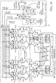
- FIG. 4 is a configuration diagram illustrating the two-way dividers 5-1 to 5-8 of the phase detector according to the second embodiment.
- Each of the two-way dividers 5-1 to 5-8 includes a transistor 5d, a transistor 5e, and a transistor 5f, and forms a current mirror circuit.
- each of the two-way dividers 5-1 to 5-8 outputs a current having the same magnitude as a current output from the terminal 5a from each of the terminal 5b and the terminal 5c.
- the transistor 5d is, for example, a field effect transistor (FET).
- FET field effect transistor
- a gate terminal of the transistor 5d is connected to each of the terminal 5a, a gate terminal of the transistor 5e, and a gate terminal of the transistor 5f.
- a voltage VCC is applied to a drain terminal of the transistor 5d.
- a source terminal of the transistor 5d is connected to each of the terminal 5a, a gate terminal of the transistor 5d, a gate terminal of the transistor 5e, and a gate terminal of the transistor 5f.
- the transistor 5e is, for example, an FET.
- a gate terminal of the transistor 5e is connected to each of the terminal 5a, a gate terminal of the transistor 5d, and a gate terminal of the transistor 5f.
- a voltage VCC is applied to a drain terminal of the transistor 5e.
- a source terminal of the transistor 5e is connected to the terminal 5b.
- the transistor 5f is, for example, an FET.
- a gate terminal of the transistor 5f is connected to each of the terminal 5a, a gate terminal of the transistor 5d, and a gate terminal of the transistor 5e.
- a voltage VCC is applied to a drain terminal of the transistor 5f.
- a source terminal of the transistor 5f is connected to the terminal 5c.
- a first subtraction circuit 7-1 includes a transistor 7-1a and a transistor 7-1b.
- the transistor 7-1a is, for example, an FET.
- a gate terminal of the transistor 7-1a is connected to each of the second addition circuit 6-2, a gate terminal of the transistor 7-1b, and a drain terminal of the transistor 7-1a.
- the drain terminal of the transistor 7-1a is connected to each of the second addition circuit 6-2, the gate terminal of the transistor 7-1a, and the gate terminal of the transistor 7-1b.
- a source terminal of the transistor 7-1a is grounded.
- the transistor 7-1b is, for example, an FET.
- the gate terminal of the transistor 7-1b is connected to each of the second addition circuit 6-2, the gate terminal of the transistor 7-1a, and the drain terminal of the transistor 7-1a.
- the drain terminal of the transistor 7-1b is connected to each of the first addition circuit 6-1 and a filter 8.
- a source terminal of the transistor 7-1b is grounded.
- a second subtraction circuit 7-2 includes a transistor 7-2a and a transistor 7-2b.
- the transistor 7-2a is, for example, an FET.
- Agate terminal of the transistor 7-2a is connected to each of the fourth addition circuit 6-4, a gate terminal of the transistor 7-2b, and a drain terminal of the transistor 7-2a.
- the drain terminal of the transistor 7-1a is connected to each of the fourth addition circuit 6-4, the gate terminal of the transistor 7-2a, and the gate terminal of the transistor 7-2b.
- a source terminal of the transistor 7-2a is grounded.
- the transistor 7-2b is, for example, an FET.
- the gate terminal of the transistor 7-2b is connected to each of the fourth addition circuit 6-4, the gate terminal of the transistor 7-1a, and the drain terminal of the transistor 7-2a.
- a drain terminal of the transistor 7-2b is connected to each of the third addition circuit 6-3 and a calculation processing circuit 9.
- a source terminal of the transistor 7-2b is grounded.
- the filter 8 is implemented by a capacitor 8a.
- the filter 8 removes a high-frequency component included in a first subtraction signal output from the first subtraction circuit 7-1.
- the filter 8 outputs the first subtraction signal after removal of the high-frequency component to the calculation processing circuit 9.
- One end of the capacitor 8a is connected to a signal line connecting an output side of the first subtraction circuit 7-1 to an input side of the calculation processing circuit 9, and the other end of the capacitor 8a is grounded.
- the transistor 11-1 When a first positive-phase signal cos ( ⁇ t) is input from the signal input terminal 1a to the transistor 11-1, the transistor 11-1 multiplies the amplitude of the first positive-phase signal cos ( ⁇ t) by ⁇ .
- the transistor 11-1 outputs the first positive-phase signal acos ( ⁇ t) obtained by multiplying the amplitude by a to an emitter terminal of each of the transistor 3-1' and the transistor 3-2'.
- the transistor 11-2 When a first negative-phase signal -cos ( ⁇ t) is input from the signal input terminal 1b to the transistor 11-2, the transistor 11-2 multiplies the amplitude of the first negative-phase signal -cos ( ⁇ t) by ⁇ .
- the transistor 11-2 outputs the first negative-phase signal -acos ( ⁇ t) obtained by multiplying the amplitude by ⁇ to an emitter terminal of each of the transistor 3-3' and the transistor 3-4'.
- the transistor 11-3 When a second positive-phase signal cos ( ⁇ t + ⁇ ) is input from the signal input terminal 1c to the transistor 11-3, the transistor 11-3 multiplies the amplitude of the second positive-phase signal cos ( ⁇ t + ⁇ ) by ⁇ .
- the transistor 11-3 outputs the second positive-phase signal acos ( ⁇ t + ⁇ ) obtained by multiplying the amplitude by ⁇ to an emitter terminal of each of the transistor 3-5' and the transistor 3-6'.
- the transistor 11-4 When a second negative-phase signal -cos ( ⁇ t + ⁇ ) is input from the signal input terminal 1d to the transistor 11-4, the transistor 11-4 multiplies the amplitude of the second negative-phase signal -cos ( ⁇ t + ⁇ ) by ⁇ .
- the transistor 11-4 outputs the second negative-phase signal -acos ( ⁇ t + ⁇ ) obtained by multiplying the amplitude by ⁇ to an emitter terminal of each of the transistor 3-7' and the transistor 3-8'.
- a phase-shifted second positive-phase signal cos ( ⁇ t + ⁇ + d) output from the phase shifter 2-3 and a first positive-phase signal acos ( ⁇ t) output from the transistor 11-1 are input to the transistor 3-1'.
- the transistor 3-1' subtracts the first positive-phase signal acos ( ⁇ t) from the phase-shifted second positive-phase signal cos ( ⁇ t + ⁇ + d).
- the transistor 3-1' multiplies the subtracted result cos ( ⁇ t + ⁇ + d) - acos ( ⁇ t) by the transconductance g n .
- the current I 1 indicated in formula (8) flows from the two-way divider 5-1 to a collector terminal of the transistor 3-1'.
- a phase-shifted second negative-phase signal -cos ( ⁇ t + ⁇ + d) output from the phase shifter 2-4 and a first positive-phase signal acos ( ⁇ t) output from the transistor 11-1 are input to the transistor 3-2'.
- the transistor 3-2' subtracts the first positive-phase signal acos ( ⁇ t) from the phase-shifted second negative-phase signal -cos ( ⁇ t + ⁇ + d).
- the transistor 3-2' multiplies the subtracted result -cos ( ⁇ t + ⁇ + d) - acos ( ⁇ t) by the transconductance g n .
- the current I 2 indicated in formula (9) flows from the two-way divider 5-2 to a collector terminal of the transistor 3-2'.
- a phase-shifted second negative-phase signal -cos ( ⁇ t + ⁇ + d) output from the phase shifter 2-4 and a first negative-phase signal -acos ( ⁇ t) output from the transistor 11-2 are input to the transistor 3-3'.
- the transistor 3-3' subtracts the first negative-phase signal -acos ( ⁇ t) from the phase-shifted second negative-phase signal -cos ( ⁇ t + ⁇ + d).
- the transistor 3-3' multiplies the subtracted result -cos ( ⁇ t + ⁇ + d) + acos ( ⁇ t) by the transconductance g n .
- the current I 3 indicated in formula (10) flows from the two-way divider 5-3 to a collector terminal of the transistor 3-3'.
- a phase-shifted second positive-phase signal cos ( ⁇ t + ⁇ + d) output from the phase shifter 2-3 and a first negative-phase signal -acos ( ⁇ t) output from the transistor 11-2 are input to the transistor 3-4'.
- the transistor 3-4' subtracts the first negative-phase signal -acos ( ⁇ t) from the phase-shifted second positive-phase signal cos ( ⁇ t + ⁇ + d).
- the transistor 3-4' multiplies the subtracted result cos ( ⁇ t + ⁇ + d) + acos ( ⁇ t) by the transconductance g n .
- the current I 4 indicated in formula (11) flows from the two-way divider 5-4 to a collector terminal of the transistor 3-4'.
- a phase-shifted first positive-phase signal cos ( ⁇ t + d) output from the phase shifter 2-1 and a second positive-phase signal acos ( ⁇ t + ⁇ ) output from the transistor 11-3 are input to the transistor 3-5'.
- the transistor 3-5' subtracts the second positive-phase signal acos ( ⁇ t + ⁇ ) from the phase-shifted first positive-phase signal cos ( ⁇ t + d).
- the transistor 3-5' multiplies the subtracted result cos ( ⁇ t + d) - acos ( ⁇ t + ⁇ ) by the transconductance g n .
- the current I 5 indicated in formula (12) flows from the two-way divider 5-5 to a collector terminal of the transistor 3-5'.
- a phase-shifted first negative-phase signal -cos ( ⁇ t + d) output from the phase shifter 2-2 and a second positive-phase signal acos ( ⁇ t + ⁇ ) output from the transistor 11-3 are input to the transistor 3-6'.
- the transistor 3-6' subtracts the second positive-phase signal acos ( ⁇ t + ⁇ ) from the phase-shifted first negative-phase signal -cos ( ⁇ t + d).
- the transistor 3-6' multiplies the subtracted result -cos ( ⁇ t + d) - acos ( ⁇ t + ⁇ ) by the transconductance g n .
- the current I 6 indicated in formula (13) flows from the two-way divider 5-6 to a collector terminal of the transistor 3-6'.
- a phase-shifted first negative-phase signal -cos ( ⁇ t + d) output from the phase shifter 2-2 and a second negative-phase signal -acos ( ⁇ t + ⁇ ) output from the transistor 11-4 are input to the transistor 3-7'.
- the transistor 3-7' subtracts the second negative-phase signal -acos ( ⁇ t + ⁇ ) from the phase-shifted first negative-phase signal -cos ( ⁇ t + d).
- the transistor 3-7' multiplies the subtracted result -cos ( ⁇ t + d) + acos ( ⁇ t + ⁇ ) by the transconductance g n .
- the current I 7 indicated in formula (14) flows from the two-way divider 5-7 to a collector terminal of the transistor 3-7'.
- a phase-shifted first positive-phase signal cos ( ⁇ t + d) output from the phase shifter 2-1 and a second negative-phase signal -acos ( ⁇ t + ⁇ ) output from the transistor 11-4 are input to the transistor 3-8'.
- the transistor 3-8' subtracts the second negative-phase signal -acos ( ⁇ t + ⁇ ) from the phase-shifted first positive-phase signal cos ( ⁇ t + d).
- the transistor 3-8' multiplies the subtracted result cos ( ⁇ t + d) + acos ( ⁇ t + ⁇ ) by the transconductance g n .
- the current I 8 indicated in formula (15) flows from the two-way divider 5-8 to a collector terminal of the transistor 3-8'.
- harmonic components included in each of the current I1 the current I 2 , the current I 3 , the current I 4 , the current I 5 , the current I 6 , the current I 7 , and the current I 8 .
- odd-order (1, 3, 5, ...) harmonic components cancel each other in a differential signal. Since the strongest component among even-order (2, 4, 6, ...) harmonic components is a second-order harmonic component, the second-order harmonic component is dominant among the even-order (2, 4, 6, %) harmonic components.
- the second-order harmonic component is represented by (x ⁇ y) 2 and includes squared component terms (x 2 , y 2 ) and a term represented by 2xy.
- the second-order harmonic component is substantially equal to the term represented by 2xy.
- each of the current I 1 , the current I 2 , the current I 3 , the current I 4 , the current I 5 , the current I 6 , the current I 7 , and the current I 8 is approximated as in formulas (16) to (23).
- the current I 3 corresponds to the third multiplication signal
- the current I 5 corresponds to the fifth multiplication signal
- the current I 7 corresponds to the seventh multiplication signal for a similar reason to the current I 1 .
- the current I 4 corresponds to the fourth multiplication signal
- the current I 6 corresponds to the sixth multiplication signal
- the current I 8 corresponds to the eighth multiplication signal for a similar reason to the current I 2 .
- the two-way divider 5-1 outputs the same current I 1 as the current I 1 output from the terminal 5a to a collector terminal of the transistor 3-1' from the terminal 5b to the first addition circuit 6-1, and outputs the current I 1 from the terminal 5c to the third addition circuit 6-3.
- the two-way divider 5-2 outputs the same current I 2 as the current I 2 output from the terminal 5a to a collector terminal of the transistor 3-2' from the terminal 5b to the second addition circuit 6-2, and outputs the current I 2 from the terminal 5c to the fourth addition circuit 6-4.
- the two-way divider 5-3 outputs the same current I 3 as the current I 3 output from the terminal 5a to a collector terminal of the transistor 3-3' from the terminal 5b to the first addition circuit 6-1, and outputs the current I 3 from the terminal 5c to the third addition circuit 6-3.
- the two-way divider 5-4 outputs the same current I 4 as the current I 4 output from the terminal 5a to a collector terminal of the transistor 3-4' from the terminal 5b to the second addition circuit 6-2, and outputs the current I 4 from the terminal 5c to the fourth addition circuit 6-4.
- the two-way divider 5-5 outputs the same current I 5 as the current I 5 output from the terminal 5a to a collector terminal of the transistor 3-5' from the terminal 5b to the first addition circuit 6-1, and outputs the current I 5 from the terminal 5c to the fourth addition circuit 6-4.
- the two-way divider 5-6 outputs the same current I 6 as the current I 6 output from the terminal 5a to a collector terminal of the transistor 3-6' from the terminal 5b to the second addition circuit 6-2, and outputs the current I 6 from the terminal 5c to the third addition circuit 6-3.
- the two-way divider 5-7 outputs the same current I 7 as the current I 7 output from the terminal 5a to a collector terminal of the transistor 3-7' from the terminal 5b to the first addition circuit 6-1, and outputs the current I 7 from the terminal 5c to the fourth addition circuit 6-4.
- the two-way divider 5-8 outputs the same current I 8 as the current I 8 output from the terminal 5a to a collector terminal of the transistor 3-8' from the terminal 5b to the second addition circuit 6-2, and outputs the current I 8 from the terminal 5c to the third addition circuit 6-3.
- the current of I 1 + I 3 + I 5 + I 7 flows through a drain terminal of the transistor 7-1b in the first subtraction circuit 7-1.
- the current of I 2 + I 4 + 1 6 + I 8 flows through each of a drain terminal of the transistor 7-1a, a gate terminal of the transistor 7-1a, and a gate terminal of the transistor 7-1b in the first subtraction circuit 7-1.
- the current of I 2 + I 4 + I 5 + I 7 flows through each of a drain terminal of the transistor 7-2a, a gate terminal of the transistor 7-2a, and a gate terminal of the transistor 7-2b in the second subtraction circuit 7-2.
- the first subtraction circuit 7-1 subtracts the current of I 2 + I 4 + I 6 + I 8 from the current of I 1 + I 3 + I 5 + I 7 .
- I OUT1 indicating a result of the subtraction by the first subtraction circuit 7-1 flows through the filter 8.
- the second subtraction circuit 7-2 subtracts the current of I 2 + I 4 + I 5 + I 7 from the current of I 1 + I 3 + I 6 + I 8 .
- the calculation processing circuit 9 calculates a phase difference ⁇ between a first differential signal and a second differential signal from the current I OUT1 ' and the current I OUT2 as indicated in the following formula (30).
- ⁇ tan ⁇ 1 I OUT 2 I OUT 1 ′ ⁇ cos d sin
- d tan ⁇ 1 ⁇ 8 ⁇ sin ⁇ sin d ⁇ 8 ⁇ cos ⁇ cos d ⁇ cos d sin d
- each of cos (d) and sin (d) is also a predetermined value.
- each of cos (d) and sin (d) may be stored in an internal memory of the calculation processing circuit 9, or may be provided from the outside of the phase detector illustrated in FIG. 3 .
- the calculation processing circuit 9 outputs the calculated phase difference ⁇ to the signal output terminal 10.
- phase difference ⁇ between a first differential signal and a second differential signal can be calculated.
- the phase shift amount d in which cos (d) or sin (d) is not zero is a phase shift amount other than 0 degrees, 90 degrees, 180 degrees, or 270 degrees.
- a range in which the phase difference ⁇ can be detected is not limited to a range of 180 degrees similarly to the phase detector illustrated in FIG. 1 .
- the phase shift amount is d.
- the first subtraction signal after removal of the high-frequency component output from the filter 8 is 8•cos ( ⁇ ) cos (45).
- the second subtraction signal output from the second subtraction circuit 7-2 is 8•sin ( ⁇ ) sin (45).
- phase difference ⁇ calculated by the calculation processing circuit 9 is indicated by the following formula (31).
- ⁇ tan ⁇ 1 ⁇ 8 ⁇ sin ⁇ sin 45 ⁇ 8 ⁇ cos ⁇ cos 45 ⁇ cos 45
- sin 45 tan ⁇ 1 ⁇ 8 ⁇ sin ⁇ sin 45 ⁇ 8 ⁇ cos ⁇ cos 45
- the calculation processing circuit 9 does not need to multiply the term cos (d)/sin (d) as indicated by formula (31), and therefore the circuit of the calculation processing circuit 9 can be simplified as compared with a case of d ⁇ 45 degrees.
- the multiplication circuit 3 includes the transistors 3-1' to 3-8', which are nonlinear elements, as the first multiplier 3-1, the second multiplier 3-2, the third multiplier 3-3, the fourth multiplier 3-4, the fifth multiplier 3-5, the sixth multiplier 3-6, the seventh multiplier 3-7, and the eighth multiplier 3-8.
- Each of the first multiplier 3-1, the second multiplier 3-2, the third multiplier 3-3, the fourth multiplier 3-4, the fifth multiplier 3-5, the sixth multiplier 3-6, the seventh multiplier 3-7, and the eighth multiplier 3-8 only needs to be a nonlinear element, and may be, for example, a three-terminal device such as an FET or a two-terminal device such as a diode.
- the phase shifter 2-1 is connected between the signal input terminal 1a and each of a gate terminal of the transistor 3-5' and a gate terminal of the transistor 3-8'
- the phase shifter 2-2 is connected between the signal input terminal 1b and each of a gate terminal of the transistor 3-6' and a gate terminal of the transistor 3-7'
- the phase shifter 2-3 is connected between the signal input terminal 1c and each of a gate terminal of the transistor 3-1' and a gate terminal of the transistor 3-4'
- the phase shifter 2-4 is connected between the signal input terminal 1d and each of a gate terminal of the transistor 3-2' and a gate terminal of the transistor 3-3'.
- the phase shifter 2-1 may be connected between the signal input terminal 1a and a gate terminal of the transistor 11-1, and the phase shifter 2-2 may be connected between the signal input terminal 1b and a gate terminal of the transistor 11-2.
- the phase shifter 2-3 may be connected between the signal input terminal 1c and a gate terminal of the transistor 11-3, and the phase shifter 2-4 may be connected between the signal input terminal 1d and a gate terminal of the transistor 11-4.
- FIG. 5 is a configuration diagram illustrating another phase detector according to the second embodiment.
- phase detector in which each of phase shifters 2-1 to 2-4 includes a high-pass filter including a resistor and a capacitor will be described.
- FIG. 6 is a configuration diagram illustrating the phase detector according to the third embodiment.
- the same reference numerals as in FIGS. 1 and 3 indicate the same or corresponding parts, and therefore description thereof is omitted.
- the phase shifter 2-1 includes a high-pass filter including a resistor 31 and a capacitor 32.
- the phase shifter 2-2 includes a high-pass filter including the resistor 31 and a capacitor 33.
- the resistor 31 is included in both the phase shifter 2-1 and the phase shifter 2-2.
- One end of the resistor 31 is connected to each of a gate terminal of a transistor 3-5', a gate terminal of a transistor 3-8', and the other end of the capacitor 32, and the other end of the resistor 31 is connected to each of a gate terminal of a transistor 3-6', a gate terminal of a transistor 3-7', and the other end of the capacitor 33.
- One end of the capacitor 32 is connected to each of a signal input terminal 1a and a gate terminal of a transistor 11-1, and the other end of the capacitor 32 is connected to one end of the resistor 31.
- One end of the capacitor 33 is connected to each of a signal input terminal 1b and a gate terminal of the transistor 11-2, and the other end of the capacitor 33 is connected to the other end of the resistor 31.
- the phase shifter 2-3 includes a high-pass filter including a resistor 34 and a capacitor 35.
- the phase shifter 2-4 includes a high-pass filter including the resistor 34 and a capacitor 36.
- the resistor 34 is included in both the phase shifter 2-3 and the phase shifter 2-4.
- One end of the resistor 34 is connected to each of a gate terminal of the transistor 3-1', a gate terminal of the transistor 3-4', and the other end of the capacitor 35, and the other end of the resistor 34 is connected to each of a gate terminal of the transistor 3-2', a gate terminal of the transistor 3-3', and the other end of the capacitor 36.
- One end of the capacitor 35 is connected to each of a signal input terminal 1c and a gate terminal of a transistor 11-3, and the other end of the capacitor 35 is connected to one end of the resistor 34.
- One end of the capacitor 36 is connected to each of a signal input terminal 1d and a gate terminal of a transistor 11-4, and the other end of the capacitor 36 is connected to the other end of the resistor 34.
- a transfer function T of each of the phase shifters 2-1 to 2-4 is represented by the following formula (32).
- T ⁇ CR ⁇ CR 2 + 4 ⁇ CR + 2 j
- R represents a resistance value of each of the resistors 31 and 34
- C represents a capacitance value of each of the capacitors 32, 33, 35, and 36.
- j represents an imaginary number.
- a voltage gain B of each of the phase shifters 2-1 to 2-4 is represented by the following formula (33), and a passage phase shift ⁇ of each of the phase shifters 2-1 to 2-4 is represented by the following formula (34).
- each of the phase shifters 2-1 to 2-4 includes a high-pass filter including a resistor and a capacitor.
- each of the phase shifters 2-1 to 2-4 includes a low-pass filter including a resistor and a capacitor may be used.
- FIG. 7 is a configuration diagram illustrating another phase detector according to the third embodiment.
- the phase shifter 2-1 includes a low-pass filter including a resistor 41 and a capacitor 42.
- the phase shifter 2-2 includes a low-pass filter including a resistor 43 and the capacitor 42.
- the capacitor 42 is included in both the phase shifter 2-1 and the phase shifter 2-2.
- One end of the capacitor 42 is connected to each of a gate terminal of the transistor 3-5', a gate terminal of the transistor 3-8', and the other end of the resistor 41, and the other end of the capacitor 42 is connected to each of a gate terminal of the transistor 3-6', a gate terminal of the transistor 3-7', and the other end of the resistor 43.
- One end of the resistor 41 is connected to each of the signal input terminal 1a and a gate terminal of the transistor 11-1, and the other end of the resistor 41 is connected to one end of the capacitor 42.
- One end of the resistor 43 is connected to each of the signal input terminal 1b and a gate terminal of the transistor 11-2, and the other end of the resistor 43 is connected to the other end of the capacitor 42.
- the phase shifter 2-3 includes a low-pass filter including a resistor 44 and a capacitor 45.
- the phase shifter 2-4 includes a low-pass filter including a resistor 46 and the capacitor 45.
- the capacitor 45 is included in both the phase shifter 2-3 and the phase shifter 2-4.
- One end of the capacitor 42 is connected to each of a gate terminal of the transistor 3-1', ae gate terminal of the transistor 3-4', and the other end of the resistor 44, and the other end of the capacitor 42 is connected to each of a gate terminal of the transistor 3-2', a gate terminal of the transistor 3-3', and the other end of the resistor 46.
- One end of the resistor 44 is connected to each of the signal input terminal 1c and a gate terminal of the transistor 11-3, and the other end of the resistor 44 is connected to one end of the capacitor 45.
- One end of the resistor 46 is connected to each of the signal input terminal 1d and a gate terminal of the transistor 11-4, and the other end of the resistor 46 is connected to the other end of the capacitor 45.
- a condition under which a passage phase shift ⁇ of each of the phase shifters 2-1 to 2-4 illustrated in FIG. 7 is, for example, 45 degrees is indicated by formula (35) similarly to the condition under which the passage phase shift ⁇ of each of the phase shifters 2-1 to 2-4 illustrated in FIG. 6 is 45 degrees.
- each of the phase shifters 2-1 to 2-4 includes a high-pass filter
- each of the phase shifters 2-1 to 2-4 includes a low-pass filter.
- each of the phase shifters 2-1 and 2-2 may include a high-pass filter
- each of the phase shifters 2-3 and 2-4 may include a low-pass filter
- each of the phase shifters 2-1 and 2-2 may include a low-pass filter
- each of the phase shifters 2-3 and 2-4 may include a high-pass filter.
- each of the phase shifters 2-1 to 2-4 includes a high-pass filter including a resistor and a capacitor.
- phase detector in which each of phase shifters 2-1 to 2-4 includes a high-pass filter including a resistor and a variable capacitor will be described.
- FIG. 8 is a configuration diagram illustrating the phase detector according to the fourth embodiment.
- the same reference numerals as in FIGS. 1 , 3 , and 6 indicate the same or corresponding parts, and therefore description thereof is omitted.
- the phase shifter 2-1 includes a high-pass filter including a resistor 31 and a variable capacitor 37.
- the phase shifter 2-2 includes a high-pass filter including the resistor 31 and a variable capacitor 38.
- variable capacitor 37 One end of the variable capacitor 37 is connected to each of a signal input terminal 1a and a gate terminal of a transistor 11-1, and the other end of the variable capacitor 37 is connected to one end of the resistor 31.
- variable capacitor 38 One end of the variable capacitor 38 is connected to each of a signal input terminal 1b and a gate terminal of a transistor 11-2, and the other end of the variable capacitor 38 is connected to the other end of the resistor 31.
- the phase shifter 2-3 includes a high-pass filter including a resistor 34 and a variable capacitor 39.
- the phase shifter 2-4 includes a high-pass filter including the resistor 34 and a variable capacitor 40.
- variable capacitor 39 One end of the variable capacitor 39 is connected to each of a signal input terminal 1c and a gate terminal of a transistor 11-3, and the other end of the variable capacitor 39 is connected to one end of the resistor 34.
- variable capacitor 40 One end of the variable capacitor 40 is connected to each of a signal input terminal 1d and a gate terminal of a transistor 11-4, and the other end of the variable capacitor 40 is connected to the other end of the resistor 34.
- a transfer function T of each of the phase shifters 2-1 to 2-4 is represented by the above formula (32).
- a voltage gain B of each of the phase shifters 2-1 to 2-4 is represented by the above formula (33), and a passage phase shift ⁇ of each of the phase shifters 2-1 to 2-4 is represented by the above formula (34).
- a condition under which the passage phase shift ⁇ is, for example, 45 degrees is represented by the above formula (35).
- a phase shift amount d of each of the phase shifters 2-1 to 2-4 can be set to, for example, 45 degrees by adjusting a capacitance value C of each of the variable capacitors 37 to 40.
- each of the phase shifters 2-1 to 2-4 includes a low-pass filter including a resistor and a capacitor.
- each of the phase shifters 2-1 to 2-4 includes a low-pass filter including a resistor and a variable capacitor will be described.
- FIG. 9 is a configuration diagram illustrating another phase detector according to the fourth embodiment.
- the same reference numerals as in FIGS. 1 , 3 , and 7 indicate the same or corresponding parts, and therefore description thereof is omitted.
- the phase shifter 2-1 includes a low-pass filter including a resistor 41 and a variable capacitor 47.
- the phase shifter 2-2 includes a low-pass filter including a resistor 43 and the variable capacitor 47.
- variable capacitor 47 is included in both the phase shifter 2-1 and the phase shifter 2-2.
- variable capacitor 47 One end of the variable capacitor 47 is connected to each of a gate terminal of a transistor 3-5', a gate terminal of a transistor 3-8', and the other end of the resistor 41, and the other end of the variable capacitor 47 is connected to each of a gate terminal of a transistor 3-6', a gate terminal of a transistor 3-7', and the other end of the resistor 43.
- the phase shifter 2-3 includes a low-pass filter including a resistor 44 and the variable capacitor 48.
- the phase shifter 2-4 includes a low-pass filter including a resistor 46 and the variable capacitor 48.
- variable capacitor 48 is included in both the phase shifter 2-3 and the phase shifter 2-4.
- variable capacitor 48 One end of the variable capacitor 48 is connected to each of a gate terminal of a transistor 3-1', a gate terminal of a transistor 3-4', and the other end of the resistor 44, and the other end of the variable capacitor 48 is connected to each of a gate terminal of a transistor 3-2', a gate terminal of a transistor 3-3', and the other end of the resistor 46.
- a condition under which a passage phase shift ⁇ of each of the phase shifters 2-1 to 2-4 illustrated in FIG. 9 is, for example, 45 degrees is indicated by formula (35) similarly to the condition under which the passage phase shift ⁇ of each of the phase shifters 2-1 to 2-4 illustrated in FIG. 8 is 45 degrees.
- a phase shift amount d of each of the phase shifters 2-1 to 2-4 can be set to, for example, 45 degrees by adjusting a capacitance value C of each of the variable capacitors 47 and 48.
- each of the phase shifters 2-1 to 2-4 includes a high-pass filter
- each of the phase shifters 2-1 to 2-4 includes a low-pass filter.
- each of the phase shifters 2-1 and 2-2 may include a high-pass filter
- each of the phase shifters 2-3 and 2-4 may include a low-pass filter
- each of the phase shifters 2-1 and 2-2 may include a low-pass filter
- each of the phase shifters 2-3 and 2-4 may include a high-pass filter.
- phase detector in which each of phase shifters 2-1 and 2-2 includes a low-pass filter including a resistor and a variable capacitor, and each of phase shifters 2-3 and 2-4 includes a high-pass filter including a resistor and a variable capacitor will be described.
- FIG. 10 is a configuration diagram illustrating the phase detector according to the fifth embodiment.
- the same reference numerals as in FIGS. 1 , 3 , 8 , and 9 indicate the same or corresponding parts, and therefore description thereof is omitted.
- a comparison circuit 50 includes a detection circuit 51, a detection circuit 52, and a comparator 53.
- the comparison circuit 50 adjusts a capacitance value C of each of the variable capacitors 47 included in the low-pass filter and the variable capacitors 39 and 40 included in the high-pass filter on the basis of an amplitude of an output signal of the low-pass filter included in the phase shifters 2-1 and 2-2 and an amplitude of an output signal of the high-pass filter included in the phase shifters 2-3 and 2-4.
- the detection circuit 51 detects an amplitude of a phase-shifted first positive-phase signal cos ( ⁇ t + d), which is an output signal of the low-pass filter included in the phase shifter 2-1, and an amplitude of a phase-shifted first negative-phase signal -cos ( ⁇ t + d), which is an output signal of the low-pass filter included in phase shifter 2-2.
- the detection circuit 51 outputs, to the comparator 53, a differential amplitude between the amplitude of the phase-shifted first positive-phase signal cos ( ⁇ t + d) and the amplitude of the phase-shifted first negative-phase signal -cos ( ⁇ t + d).
- the detection circuit 52 detects an amplitude of a phase-shifted second positive-phase signal cos ( ⁇ t + ⁇ + d), which is an output signal of the high-pass filter included in phase shifter 2-3, and an amplitude of a phase-shifted second negative-phase signal -cos ( ⁇ t + ⁇ + d), which is an output signal of the high-pass filter included in phase shifter 2-4.
- the detection circuit 52 outputs, to the comparator 53, a differential amplitude between the amplitude of the phase-shifted second positive-phase signal cos ( ⁇ t + ⁇ + d) and the amplitude of the phase-shifted second negative-phase signal -cos ( ⁇ t + ⁇ + d).
- the comparator 53 compares the differential amplitude output from the detection circuit 51 with the differential amplitude output from the detection circuit 52.
- the comparator 53 adjusts a capacitance value C of each of the variable capacitor 47 included in the low-pass filter and the variable capacitors 39 and 40 included in the high-pass filter on the basis of a comparison result of the differential amplitudes.
- FIG. 11A is an explanatory diagram illustrating frequency characteristics of a pass gain in the low-pass filter included in the phase shifters 2-1 and 2-2 and the high-pass filter included in the phase shifters 2-3 and 2-4.
- FIG. 11B is an explanatory diagram illustrating frequency characteristics of a pass phase shift in the low-pass filter included in the phase shifters 2-1 and 2-2 and the high-pass filter included in the phase shifters 2-3 and 2-4.
- the detection circuit 51 detects an amplitude of a phase-shifted first positive-phase signal cos ( ⁇ t + d), which is an output signal of the low-pass filter included in the phase shifter 2-1.
- the detection circuit 51 detects an amplitude of a phase-shifted first negative-phase signal -cos ( ⁇ t + d), which is an output signal of the low-pass filter included in the phase shifter 2-2.
- the detection circuit 51 outputs, to the comparator 53, a differential amplitude between the amplitude of the phase-shifted first positive-phase signal cos ( ⁇ t + d) and the amplitude of the phase-shifted first negative-phase signal -cos ( ⁇ t + d).
- the detection circuit 52 detects an amplitude of a phase-shifted second positive-phase signal cos ( ⁇ t + ⁇ + d), which is an output signal of the high-pass filter included in the phase shifter 2-3.
- the detection circuit 52 detects an amplitude of a phase-shifted second negative-phase signal -cos ( ⁇ t + ⁇ + d), which is an output signal of the high-pass filter included in the phase shifter 2-4.
- the detection circuit 52 outputs, to the comparator 53, a differential amplitude between the amplitude of the phase-shifted second positive-phase signal cos ( ⁇ t + ⁇ + d) and the amplitude of the phase-shifted second negative-phase signal -cos ( ⁇ t + ⁇ + d).
- the comparator 53 compares the differential amplitude output from the detection circuit 51 with the differential amplitude output from the detection circuit 52.
- the comparator 53 adjusts a capacitance value C of each of the variable capacitor 47, the variable capacitor 39, and the variable capacitor 40 in such a manner that the differential amplitude output from detection circuit 51 coincides with the differential amplitude output from detection circuit 52.
- phase shift amount d in each of phase shifters 2-1 to 2-4 is 45 degrees.
- the comparator 53 adjusts a capacitance value C of each of the variable capacitor 47, the variable capacitor 39, and the variable capacitor 40 in such a manner that the differential amplitude output from detection circuit 51 coincides with the differential amplitude output from detection circuit 52.
- coincidence of the differential amplitudes is not limited to exact coincidence, and the differential amplitudes may be different from each other in a range in which there is no practical problem.
- each of the phase shifters 2-1 and 2-2 includes a low-pass filter, and each of the phase shifters 2-3 and 2-4 includes a high-pass filter.
- each of the phase shifters 2-1 to 2-2 may include a high-pass filter, and each of the phase shifters 2-3 to 2-4 may include a low-pass filter.
- FIG. 12 is a configuration diagram illustrating another phase detector according to the fifth embodiment.
- the comparator 53 adjusts a capacitance value C of each of the variable capacitor 37, the variable capacitor 38, and the variable capacitor 48 in such a manner that the differential amplitude output from the detection circuit 51 coincides with the differential amplitude output from the detection circuit 52.
- the phase difference calculating circuit 4 includes the first addition circuit 6-1, the second addition circuit 6-2, the third addition circuit 6-3, and the fourth addition circuit 6-4.
- a phase detector in which a phase difference calculating circuit 4 includes a first difference circuit 60-1, a second difference circuit 60-2, a third difference circuit 60-3, and a fourth difference circuit 60-4 will be described.
- FIG. 13 is a configuration diagram illustrating the phase detector according to the sixth embodiment.
- the same reference numerals as in FIG. 1 indicate the same or corresponding parts, and therefore description thereof is omitted.
- the phase difference calculating circuit 4 includes two-way dividers 5-1 to 5-8, the first difference circuit 60-1, the second difference circuit 60-2, the third difference circuit 60-3, the fourth difference circuit 60-4, a first subtraction circuit 61-1, a second subtraction circuit 61-2, a filter 62, a calculation processing circuit 63, and a signal output terminal 10.
- each of the first difference circuit 60-1, the second difference circuit 60-2, the third difference circuit 60-3, and the fourth difference circuit 60-4 is represented by "-".
- the first difference circuit 60-1 subtracts a sum of a fifth multiplication signal cos ( ⁇ t + d) ⁇ cos ( ⁇ t + ⁇ ) output from the two-way divider 5-5 and a seventh multiplication signal cos ( ⁇ t + d) ⁇ cos ( ⁇ t + ⁇ ) output from the two-way divider 5-7 from a sum of a first multiplication signal cos ( ⁇ t) ⁇ cos ( ⁇ t + ⁇ + d) output from the two-way divider 5-1 and a third multiplication signal cos ( ⁇ t) ⁇ cos( ⁇ t + ⁇ + d) output from the two-way divider 5-3.
- the first difference circuit 60-1 outputs a first difference signal -4•sin ( ⁇ ) sin (d) indicating a result of the subtraction to the first subtraction circuit 61-1.
- the second difference circuit 60-2 subtracts a sum of a sixth multiplication signal -cos ( ⁇ t + d) ⁇ cos ( ⁇ t + ⁇ ) output from the two-way divider 5-6 and an eighth multiplication signal -cos ( ⁇ t + d) ⁇ cos ( ⁇ t + ⁇ ) output from the two-way divider 5-8 from a sum of a second multiplication signal -cos ( ⁇ t) ⁇ cos ( ⁇ t + ⁇ + d) output from the two-way divider 5-2 and a fourth multiplication signal -cos ( ⁇ t) ⁇ cos ( ⁇ t + ⁇ + d) output from the two-way divider 5-4.
- the second difference circuit 60-2 outputs a second difference signal 4•sin ( ⁇ ) sin (d) indicating a result of the subtraction to the first subtraction circuit 61-1.
- the third difference circuit 60-3 subtracts a sum of the sixth multiplication signal -cos ( ⁇ t + d) ⁇ cos ( ⁇ t + ⁇ ) output from the two-way divider 5-6 and the eighth multiplication signal -cos ( ⁇ t + d) ⁇ cos ( ⁇ t + ⁇ ) output from the two-way divider 5-8 from a sum of the first multiplication signal cos ( ⁇ t) ⁇ cos ( ⁇ t + ⁇ + d) output from the two-way divider 5-1 and the third multiplication signal cos ( ⁇ t) ⁇ cos( ⁇ t + ⁇ + d) output from the two-way divider 5-3.
- the third difference circuit 60-3 outputs a third difference signal 2•(cos (2 ⁇ t + ⁇ + d) + cos ( ⁇ + d) + cos ( ⁇ - d)) indicating a result of the subtraction to the second subtraction circuit 61-2.
- the fourth difference circuit 60-4 subtracts a sum of the fifth multiplication signal cos ( ⁇ t + d) ⁇ cos ( ⁇ t + ⁇ ) output from the two-way divider 5-5 and the seventh multiplication signal cos ( ⁇ t + d) ⁇ cos ( ⁇ t + ⁇ ) output from the two-way divider 5-7 from a sum of the second multiplication signal -cos ( ⁇ t) ⁇ cos ( ⁇ t + ⁇ + d) output from the two-way divider 5-2 and the fourth multiplication signal -cos ( ⁇ t) ⁇ cos ( ⁇ t + ⁇ + d) output from the two-way divider 5-4.
- the fourth difference circuit 60-4 outputs a fourth difference signal -2•(cos (2 ⁇ t + ⁇ + d) + cos ( ⁇ + d) + cos ( ⁇ - d)) indicating a result of the subtraction to the second subtraction circuit 61-2.
- the first subtraction circuit 61-1 subtracts the second difference signal 4•sin ( ⁇ ) sin (d) output from the second difference circuit 60-2 from the first difference signal -4•sin ( ⁇ ) sin (d) output from the first difference circuit 60-1.
- the first subtraction circuit 61-1 outputs a first subtraction signal -8•sin ( ⁇ ) sin (d) indicating a result of the subtraction to the calculation processing circuit 63.
- the second subtraction circuit 61-2 subtracts the third difference signal 2•(cos (2 ⁇ t + ⁇ + d) + cos ( ⁇ + d) + cos ( ⁇ - d)) output from the third difference circuit 60-3 from the fourth difference signal -2•(cos (2 ⁇ t + ⁇ + d) + cos ( ⁇ + d) + cos ( ⁇ - d)) output from the fourth difference circuit 60-4.
- the second subtraction circuit 61-2 outputs a second subtraction signal -4•cos (2 ⁇ t + ⁇ + d) indicating a result of the subtraction to the filter 62.
- the filter 62 is implemented by, for example, LPF or BPF.
- the filter 62 removes a high-frequency component included in the second subtraction signal -4•cos (2 ⁇ t + ⁇ + d) output from the second subtraction circuit 61-2.
- the filter 62 outputs the second subtraction signal -8•cos ( ⁇ ) cos (d) after removal of the high-frequency component to the calculation processing circuit 63.
- the calculation processing circuit 63 calculates a phase difference ⁇ between a first differential signal and a second differential signal from the first subtraction signal - 8•sin ( ⁇ ) sin (d) output from the first subtraction circuit 61-1 and the second subtraction signal -8•cos ( ⁇ ) cos (d) after removal of the high-frequency component output from the filter 62.
- the calculation processing circuit 63 outputs the calculated phase difference ⁇ to the signal output terminal 10.
- the operation of the phase detector illustrated in FIG. 13 is similar to the operation of the phase detector illustrated in FIG. 1 except for the first difference circuit 60-1, the second difference circuit 60-2, the third difference circuit 60-3, the fourth difference circuit 60-4, the first subtraction circuit 61-1, the second subtraction circuit 61-2, the filter 62, and the calculation processing circuit 63. Therefore, only operations of the first difference circuit 60-1, the second difference circuit 60-2, the third difference circuit 60-3, the fourth difference circuit 60-4, the first subtraction circuit 61-1, the second subtraction circuit 61-2, the filter 62, and the calculation processing circuit 63 will be described here.
- the first multiplication signal cos ( ⁇ t) ⁇ cos ( ⁇ t + ⁇ + d) output from the two-way divider 5-1 and the third multiplication signal cos ( ⁇ t) ⁇ cos ( ⁇ t + ⁇ + d) output from the two-way divider 5-3 are input.
- the fifth multiplication signal cos ( ⁇ t + d) ⁇ cos ( ⁇ t + ⁇ ) output from the two-way divider 5-5 and the seventh multiplication signal cos ( ⁇ t + d) ⁇ cos ( ⁇ t + ⁇ ) output from the two-way divider 5-7 are input.
- the first difference circuit 60-1 subtracts a sum of the fifth multiplication signal cos ( ⁇ t + d) ⁇ cos ( ⁇ t + ⁇ ) and the seventh multiplication signal cos ( ⁇ t + d) ⁇ cos ( ⁇ t + ⁇ ) from a sum of the first multiplication signal cos ( ⁇ t) ⁇ cos ( ⁇ t + ⁇ + d) and the third multiplication signal cos ( ⁇ t) ⁇ cos ( ⁇ t + ⁇ + d).
- the first difference circuit 60-1 outputs a first difference signal -4•sin ( ⁇ ) sin (d) indicating a result of the subtraction to the first subtraction circuit 61-1.
- the second multiplication signal -cos ( ⁇ t) ⁇ cos ( ⁇ t + ⁇ + d) output from the two-way divider 5-2 and the fourth multiplication signal -cos ( ⁇ t) ⁇ cos ( ⁇ t + ⁇ + d) output from the two-way divider 5-4 are input.
- the sixth multiplication signal -cos ( ⁇ t + d) ⁇ cos ( ⁇ t + ⁇ ) output from the two-way divider 5-6 and the eighth multiplication signal -cos ( ⁇ t + d) ⁇ cos ( ⁇ t + ⁇ ) output from the two-way divider 5-8 are input.
- the second difference circuit 60-2 subtracts a sum of the sixth multiplication signal -cos ( ⁇ t + d) ⁇ cos ( ⁇ t + ⁇ ) and the eighth multiplication signal -cos ( ⁇ t + d) ⁇ cos ( ⁇ t + ⁇ ) from a sum of the second multiplication signal -cos ( ⁇ t) ⁇ cos ( ⁇ t + ⁇ + d) and the fourth multiplication signal -cos ( ⁇ t) ⁇ cos ( ⁇ t + ⁇ + d).
- the second difference circuit 60-2 outputs a second difference signal 4•sin ( ⁇ ) sin (d) indicating a result of the subtraction to the first subtraction circuit 61-1.
- the first multiplication signal cos ( ⁇ t) ⁇ cos ( ⁇ t + ⁇ + d) output from the two-way divider 5-1 and the third multiplication signal cos ( ⁇ t) ⁇ cos ( ⁇ t + ⁇ + d) output from the two-way divider 5-3 are input.
- the sixth multiplication signal -cos ( ⁇ t + d) ⁇ cos ( ⁇ t + ⁇ ) output from the two-way divider 5-6 and the eighth multiplication signal -cos ( ⁇ t + d) ⁇ cos ( ⁇ t + ⁇ ) output from the two-way divider 5-8 are input.
- the third difference circuit 60-3 subtracts a sum of the sixth multiplication signal -cos ( ⁇ t + d) ⁇ cos ( ⁇ t + ⁇ ) and the eighth multiplication signal -cos ( ⁇ t + d) ⁇ cos ( ⁇ t + ⁇ ) from a sum of the first multiplication signal cos ( ⁇ t) ⁇ cos ( ⁇ t + ⁇ + d) and the third multiplication signal cos ( ⁇ t) ⁇ cos ( ⁇ t + ⁇ + d).
- the third difference circuit 60-3 outputs a third difference signal 2•(cos (2 ⁇ t + ⁇ + d) + cos ( ⁇ + d) + cos ( ⁇ - d)) indicating a result of the subtraction to the second subtraction circuit 61-2.
- the second multiplication signal -cos ( ⁇ t) ⁇ cos ( ⁇ t + ⁇ + d) output from the two-way divider 5-2 and the fourth multiplication signal -cos ( ⁇ t) ⁇ cos ( ⁇ t + ⁇ + d) output from the two-way divider 5-4 are input.
- the fifth multiplication signal cos ( ⁇ t + d) ⁇ cos ( ⁇ t + ⁇ ) output from the two-way divider 5-5 and the seventh multiplication signal cos ( ⁇ t + d) ⁇ cos ( ⁇ t + ⁇ ) output from the two-way divider 5-7 are input.
- the fourth difference circuit 60-4 subtracts a sum of the fifth multiplication signal cos ( ⁇ t + d) ⁇ cos ( ⁇ t + ⁇ ) and the seventh multiplication signal cos ( ⁇ t + d) ⁇ cos ( ⁇ t + ⁇ ) from a sum of the second multiplication signal -cos ( ⁇ t) ⁇ cos ( ⁇ t + ⁇ + d) and the fourth multiplication signal -cos ( ⁇ t) ⁇ cos ( ⁇ t + ⁇ + d).
- the fourth difference circuit 60-4 outputs a fourth difference signal -2•(cos (2 ⁇ t + ⁇ + d) + cos ( ⁇ + d) + cos ( ⁇ - d)) indicating a result of the subtraction to the second subtraction circuit 61-2.
- the first difference signal -4•sin ( ⁇ ) sin (d) output from first difference circuit 60-1 and 4•sin ( ⁇ ) sin (d) output from second difference circuit 60-2 are input.
- the first subtraction circuit 61-1 subtracts the second difference signal 4•sin ( ⁇ ) sin (d) output from the second difference circuit 60-2 from the first difference signal -4•sin ( ⁇ ) sin (d).
- the first subtraction circuit 61-1 outputs a first subtraction signal -8•sin ( ⁇ ) sin (d) indicating a result of the subtraction to the calculation processing circuit 63.
- the fourth difference signal -2•(cos (2 ⁇ t + ⁇ + d) + cos ( ⁇ + d) + cos ( ⁇ - d)) output from the fourth difference circuit 60-4 and the third difference signal 2•(cos (2 ⁇ t + ⁇ + d) + cos ( ⁇ + d) + cos ( ⁇ - d)) output from the third difference circuit 60-3 are input.
- the second subtraction circuit 61-2 subtracts the third difference signal 2•(cos (2 ⁇ t + ⁇ + d) + cos ( ⁇ + d) + cos ( ⁇ - d)) from the fourth difference signal -2•(cos (2 ⁇ t + ⁇ + d) + cos ( ⁇ + d) + cos ( ⁇ - d)).
- the second subtraction circuit 61-2 outputs a second subtraction signal -4•cos (2 ⁇ t + ⁇ + d) indicating a result of the subtraction to the filter 62.
- the filter 62 When receiving the second subtraction signal -4•cos (2 ⁇ t + ⁇ + d) from the second subtraction circuit 61-2, the filter 62 removes a high-frequency component included in the second subtraction signal -4•cos (2 ⁇ t + ⁇ + d).
- the filter 62 outputs the second subtraction signal -8•cos ( ⁇ ) cos (d) after removal of the high-frequency component to the calculation processing circuit 63.
- the first subtraction signal -8•sin ( ⁇ ) sin (d) output from the first subtraction circuit 61-1 and the second subtraction signal - 8•cos ( ⁇ ) cos (d) after removal of the high-frequency component output from the filter 62 are input.
- the calculation processing circuit 63 calculates a phase difference ⁇ between a first differential signal and a second differential signal from the first subtraction signal - 8•sin ( ⁇ ) sin (d) and the second subtraction signal -8•cos ( ⁇ ) cos (d) after removal of the high-frequency component as indicated in the following formula (36).
- ⁇ tan ⁇ 1 ⁇ 8 ⁇ sin ⁇ sin d ⁇ 8 ⁇ cos ⁇ cos d ⁇ cos d sin d
- each of cos (d) and sin (d) is also a predetermined value.
- each of cos (d) and sin (d) may be stored in an internal memory of the calculation processing circuit 63, or may be provided from the outside of the phase detector illustrated in FIG. 13 .
- the calculation processing circuit 63 outputs the calculated phase difference ⁇ to the signal output terminal 10.
- phase difference ⁇ between a first differential signal and a second differential signal can be calculated.
- the phase shift amount d in which cos (d) or sin (d) is not zero is a phase shift amount other than 0 degrees, 90 degrees, 180 degrees, or 270 degrees.
- a range in which the phase difference ⁇ can be detected is not limited to a range of 180 degrees.
- the present invention is suitable for a phase detector that calculates a phase difference between a first differential signal and a second differential signal.
Landscapes
- Physics & Mathematics (AREA)
- General Physics & Mathematics (AREA)
- Engineering & Computer Science (AREA)
- Power Engineering (AREA)
- Amplifiers (AREA)
- Networks Using Active Elements (AREA)
Abstract
Description
- The present invention relates to a phase detector that calculates a phase difference between a first differential signal and a second differential signal.
- Non-Patent
Literature 1 below discloses a phase detector that detects a phase difference ϕ between two signals using a multiplier. The multiplier included in the phase detector multiplies two signals and outputs a multiplication signal indicating a multiplication result of the two signals. When the frequencies of the two signals are equal to each other, a DC component included in the multiplication signal output from the multiplier is a DC voltage proportional to cos ϕ that is a cosine of a phase difference ϕ between the two signals. - Non-Patent Literature 1: A Precise 360°-Range Phase Detector for fdNIRS Application Using a Pair of XNORs
- In the phase detector disclosed in
Non-Patent Literature 1, when the frequencies of two signals are equal to each other, a DC component included in the multiplication signal output from the multiplier is a DC voltage proportional to cos ϕ. A value of the DC voltage proportional to cos ϕ when a phase difference ϕ between two signals is in a range of 0 degrees to 180 degrees is the same as a value of the DC voltage proportional to cos ϕ when the phase difference ϕ is in a range of 180 degrees to 360 degrees. - Therefore, a range in which the phase detector disclosed in
Non-Patent Literature 1 can detect the phase difference ϕ between two signals is limited to the range of 180 degrees disadvantageously. - The present invention has been made in order to solve the above problems, and an object thereof is to obtain a phase detector capable of calculating a phase difference between a first differential signal and a second differential signal without limiting a detection range of a phase difference to a range of 180 degrees.
- A phase detector according to the present invention includes: a phase shift circuit to phase-shift each of a first positive-phase signal included in a first differential signal and a first negative-phase signal included in the first differential signal, and phase-shift each of a second positive-phase signal included in a second differential signal and a second negative-phase signal included in the second differential signal; a multiplication circuit to perform multiplication of two signals for all combinations of the first positive-phase signal included in the first differential signal and the first negative-phase signal included in the first differential signal with the second positive-phase signal phase-shifted by the phase shift circuit and the second negative-phase signal phase-shifted by the phase shift circuit, output a multiplication signal indicating a result of the multiplication, perform multiplication of two signals for all combinations of the first positive-phase signal phase-shifted by the phase shift circuit and the first negative-phase signal phase-shifted by the phase shift circuit with the second positive-phase signal included in the second differential signal and the second negative-phase signal included in the second differential signal, and output a multiplication signal indicating a result of the multiplication; and a phase difference calculating circuit to calculate a phase difference between the first differential signal and the second differential signal using all the multiplication signals output from the multiplication circuit.
- According to the present invention, a phase difference between a first differential signal and a second differential signal can be calculated without limiting a detection range of the phase difference to a range of 180 degrees.
-
-
FIG. 1 is a configuration diagram illustrating a phase detector according to a first embodiment. -
FIG. 2 is a configuration diagram illustrating an example of a phase shifter 2-1 implemented by a lumped constant circuit. -
FIG. 3 is a configuration diagram illustrating a phase detector according to a second embodiment. -
FIG. 4 is a configuration diagram illustrating two-way dividers 5-1 to 5-8 of the phase detector according to the second embodiment. -
FIG. 5 is a configuration diagram illustrating another phase detector according to the second embodiment. -
FIG. 6 is a configuration diagram illustrating a phase detector according to a third embodiment. -
FIG. 7 is a configuration diagram illustrating another phase detector according to the third embodiment. -
FIG. 8 is a configuration diagram illustrating a phase detector according to a fourth embodiment. -
FIG. 9 is a configuration diagram illustrating another phase detector according to the fourth embodiment. -
FIG. 10 is a configuration diagram illustrating a phase detector according to a fifth embodiment. -
FIG. 11A is an explanatory diagram illustrating frequency characteristics of pass gain in a low-pass filter included in phase shifters 2-1 and 2-2 and a high-pass filter included in phase shifters 2-3 and 2-4, andFIG. 11B is an explanatory diagram illustrating frequency characteristics of pass phase shift in the low-pass filter included in the phase shifters 2-1 and 2-2 and the high-pass filter included in the phase shifters 2-3 and 2-4. -
FIG. 12 is a configuration diagram illustrating another phase detector according to the fifth embodiment. -
FIG. 13 is a configuration diagram illustrating a phase detector according to a sixth embodiment. - Hereinafter, in order to describe the present invention in more detail, embodiment for carrying out the present invention will be described with reference to the accompanying drawings.
-
FIG. 1 is a configuration diagram illustrating a phase detector according to a first embodiment. - In
FIG. 1 , asignal input terminal 1a is a terminal for inputting cos (ωt) as a first positive-phase signal included in a first differential signal that is a radio frequency signal. ω represents an angular frequency, and t represents time. - A
signal input terminal 1b is a terminal for inputting -cos (ωt) as a first negative-phase signal included in the first differential signal. - A
signal input terminal 1c is a terminal for inputting cos (ωt + ϕ) as a second positive-phase signal included in a second differential signal that is a radio frequency signal. - A
signal input terminal 1d is a terminal for inputting -cos (ωt + ϕ) as a second negative-phase signal included in the second differential signal. - ϕ represents a phase difference between the first positive-phase signal cos (ωt) and the second positive-phase signal cos (ωt + ϕ), and represents a phase difference between the first negative-phase signal -cos (ωt) and the second negative-phase signal - cos (ωt + ϕ).
- A
phase shift circuit 2 includes a phase shifter 2-1, a phase shifter 2-2, a phase shifter 2-3, and a phase shifter 2-4. InFIG. 1 , each of the phase shifter 2-1, the phase shifter 2-2, the phase shifter 2-3, and the phase shifter 2-4 is represented by "d". - The
phase shift circuit 2 phase-shifts each of the first positive-phase signal cos (ωt), the first negative-phase signal -cos (ωt), the second positive-phase signal cos (ωt + ϕ), and the second negative-phase signal -cos (ωt + ϕ) by a phase shift amount d. The phase shift amount d may be stored in an internal memory of thephase shift circuit 2, or may be provided from the outside of the phase detector illustrated inFIG. 1 . - The
phase shift circuit 2 outputs each of a phase-shifted first positive-phase signal cos (ωt + d), a phase-shifted first negative-phase signal -cos (ωt + d), a phase-shifted second positive-phase signal cos (ωt + ϕ + d), and a phase-shifted second negative-phase signal -cos (ωt + ϕ + d) to amultiplication circuit 3 described later. - An input terminal 2-1a of the phase shifter 2-1 is connected to a
signal input terminal 1a, and an output terminal 2-1b of the phase shifter 2-1 is connected to each of an input terminal 3-5b of a fifth multiplier 3-5 described later and an input terminal 3-8b of an eighth multiplier 3-8 described later. - When the first positive-phase signal cos (ωt) input from the
signal input terminal 1a is input from the input terminal 2-1a to the phase shifter 2-1, the phase shifter 2-1 phase-shifts the first positive-phase signal cos (ωt) by the phase shift amount d, and outputs the phase-shifted first positive-phase signal cos (ωt + d) to each of the fifth multiplier 3-5 and the eighth multiplier 3-8 from the output terminal 2-1b. - An input terminal 2-2a of the phase shifter 2-2 is connected to a
signal input terminal 1b, and an output terminal 2-2b of the phase shifter 2-2 is connected to each of an input terminal 3-6b of a sixth multiplier 3-6 described later and an input terminal 3-7b of a seventh multiplier 3-7 described later. - When the first negative-phase signal -cos (ωt) input from the signal input terminal Ibis input from the input terminal 2-2a to the phase shifter 2-2, the phase shifter 2-2 phase-shifts the first negative-phase signal -cos (ωt) by the phase shift amount d, and outputs the phase-shifted first negative-phase signal -cos (ωt + d) to each of the sixth multiplier 3-6 and the seventh multiplier 3-7 from the output terminal 2-2b.
- An input terminal 2-3a of the phase shifter 2-3 is connected to a
signal input terminal 1c, and an output terminal 2-3b of the phase shifter 2-3 is connected to each of an input terminal 3-1b of a first multiplier 3-1 described later and an input terminal 3-4b of a fourth multiplier 3-4 described later. - When the second positive-phase signal cos (ωt + ϕ) input from the
signal input terminal 1c is input from the input terminal 2-3a to the phase shifter 2-3, the phase shifter 2-3 phase-shifts the second positive-phase signal cos (ωt + ϕ) by the phase shift amount d, and outputs the phase-shifted second positive-phase signal cos (ωt + ϕ +d) to each of the first multiplier 3-1 and the fourth multiplier 3-4 from the output terminal 2-3b. - An input terminal 2-4a of the phase shifter 2-4 is connected to a
signal input terminal 1d, and an output terminal 2-4b of the phase shifter 2-4 is connected to each of an input terminal 3-2b of a second multiplier 3-2 described later and an input terminal 3-3b of a third multiplier 3-3 described later. - When the second negative-phase signal -cos (ωt + ϕ) input from the
signal input terminal 1d is input from the input terminal 2-4a to the phase shifter 2-4, the phase shifter 2-4 phase-shifts the second negative-phase signal -cos (ωt + ϕ) by the phase shift amount d, and outputs the phase-shifted second negative-phase signal -cos (ωt + ϕ+ d) to each of the second multiplier 3-2 and the third multiplier 3-3 from the output terminal 2-4b. - The
multiplication circuit 3 includes the first multiplier 3-1, the second multiplier 3-2, the third multiplier 3-3, the fourth multiplier 3-4, the fifth multiplier 3-5, the sixth multiplier 3-6, the seventh multiplier 3-7, and the eighth multiplier 3-8. InFIG. 1 , each of the first multiplier 3-1, the second multiplier 3-2, the third multiplier 3-3, the fourth multiplier 3-4, the fifth multiplier 3-5, the sixth multiplier 3-6, the seventh multiplier 3-7, and the eighth multiplier 3-8 is represented by "×". - The
multiplication circuit 3 performs multiplication of two signals for all combinations of the first positive-phase signal cos (ωt) included in the first differential signal and the first negative-phase signal -cos (ωt) included in the first differential signal with the second positive-phase signal cos (ωt + ϕ + d) phase-shifted by thephase shift circuit 2 and the second negative-phase signal -cos (ωt + ϕ + d) phase-shifted by thephase shift circuit 2. - The
multiplication circuit 3 outputs each of cos (ωt) × cos (ωt + ϕ + d), -cos (ωt) × cos (ωt + ϕ + d), cos (ωt) × cos (ωt + ϕ + d), and -cos (ωt) × cos (ωt + ϕ + d) to a phasedifference calculating circuit 4 as a multiplication signal indicating a result of the multiplication. - The
multiplication circuit 3 performs multiplication of two signals for all combinations of the first positive-phase signal cos (ωt + d) phase-shifted by thephase shift circuit 2 and the first negative-phase signal -cos (ωt + d) phase-shifted by thephase shift circuit 2, and the second positive-phase signal cos (ωt + ϕ) included in the second differential signal and the second negative-phase signal -cos (ωt + ϕ) included in the second differential signal. - The
multiplication circuit 3 outputs each of cos (ωt + d) × cos (ωt + ϕ), -cos (ωt + d) × cos (ωt + ϕ), cos (ωt + d) × cos (ωt + ϕ), and -cos (ωt + d) × cos (ωt + ϕ) to the phasedifference calculating circuit 4 as a multiplication signal indicating a result of the multiplication. - An input terminal 3-1a of the first multiplier 3-1 is connected to the
signal input terminal 1a, the input terminal 3-1b of the first multiplier 3-1 is connected to the output terminal 2-3b of the phase shifter 2-3, and an output terminal 3-1c of the first multiplier 3-1 is connected to a two-way divider 5-1 described later. - The first positive-phase signal cos (ωt) input from the
signal input terminal 1a is input to the input terminal 3-1a of the first multiplier 3-1. - The phase-shifted second positive-phase signal cos (ωt + ϕ + d) output from the phase shifter 2-3 is input to the input terminal 3-1b of the first multiplier 3-1.
- The first multiplier 3-1 multiplies the first positive-phase signal cos (ωt) by the phase-shifted second positive-phase signal cos (ωt + ϕ + d), and outputs a first multiplication signal cos (ωt) × cos (ωt + ϕ + d) indicating a result of the multiplication to the two-way divider 5-1.
- An input terminal 3-2a of the second multiplier 3-2 is connected to the
signal input terminal 1a, the input terminal 3-2b of the second multiplier 3-2 is connected to the output terminal 2-4b of the phase shifter 2-4, and an output terminal 3-2c of the second multiplier 3-2 is connected to a two-way divider 5-2 described later. - The first positive-phase signal cos (ωt) input from the
signal input terminal 1a is input to the input terminal 3-2a of the second multiplier 3-2. - The phase-shifted second negative-phase signal -cos (ωt + ϕ + d) output from the phase shifter 2-4 is input to the input terminal 3-2b of the second multiplier 3-2.
- The second multiplier 3-2 multiplies the first positive-phase signal cos (ωt) by the phase-shifted second negative-phase signal -cos (ωt + ϕ + d), and outputs a second multiplication signal -cos (ωt) × cos (ωt + ϕ + d) indicating a result of the multiplication to the two-way divider 5-2.
- An input terminal 3-3a of the third multiplier 3-3 is connected to the
signal input terminal 1b, the input terminal 3-3b of the third multiplier 3-3 is connected to the output terminal 2-4b of the phase shifter 2-4, and an output terminal 3-3c of the third multiplier 3-3 is connected to a two-way divider 5-3 described later. - The first negative-phase signal -cos (ωt) input from the
signal input terminal 1b is input to the input terminal 3-3a of the third multiplier 3-3. - The phase-shifted second second negative-phase signal -cos (ωt + ϕ + d) output from the phase shifter 2-4 is input to the input terminal 3-3b of the third multiplier 3-3.
- The third multiplier 3-3 multiplies the first negative-phase signal -cos (ωt) by the phase-shifted second negative-phase signal -cos (ωt + ϕ + d), and outputs a third multiplication signal cos (ωt) × cos (ωt + ϕ + d) indicating a result of the multiplication to the two-way divider 5-3.
- An input terminal 3-4a of the fourth multiplier 3-4 is connected to the
signal input terminal 1b, the input terminal 3-4b of the fourth multiplier 3-4 is connected to the output terminal 2-3b of the phase shifter 2-3, and an output terminal 3-4c of the fourth multiplier 3-4 is connected to a two-way divider 5-4 described later. - The first negative-phase signal -cos (ωt) input from the
signal input terminal 1b is input to the input terminal 3-4a of the fourth multiplier 3-4. - The phase-shifted second positive-phase signal cos (ωt + ϕ + d) output from the phase shifter 2-3 is input to the input terminal 3-4b of the fourth multiplier 3-4.
- The fourth multiplier 3-4 multiplies the first negative-phase signal -cos (ωt) by the phase-shifted second positive-phase signal cos (ωt + ϕ + d), and outputs a fourth multiplication signal -cos (ωt) × cos (ωt + ϕ + d) indicating a result of the multiplication to the two-way divider 5-4.
- An input terminal 3-5a of the fifth multiplier 3-5 is connected to the
signal input terminal 1c, the input terminal 3-5b of the fifth multiplier 3-5 is connected to the output terminal 2-1b of the phase shifter 2-1, and an output terminal 3-5c of the fifth multiplier 3-5 is connected to a two-way divider 5-5 described later. - The second positive-phase signal cos (ωt + ϕ) input from the
signal input terminal 1c is input to the input terminal 3-5a of the fifth multiplier 3-5. - The phase-shifted first positive-phase signal cos (ωt + d) output from the phase shifter 2-1 is input to the input terminal 3-5b of the fifth multiplier 3-5.
- The fifth multiplier 3-5 multiplies the second positive-phase signal cos (ωt + ϕ) by the phase-shifted first positive-phase signal cos (ωt + d), and outputs a fifth multiplication signal cos (ωt + d) × cos (ωt + ϕ) indicating a result of the multiplication to the two-way divider 5-5.
- An input terminal 3-6a of the sixth multiplier 3-6 is connected to the
signal input terminal 1c, the input terminal 3-6b of the sixth multiplier 3-6 is connected to the output terminal 2-2b of the phase shifter 2-2, and an output terminal 3-6c of the sixth multiplier 3-6 is connected to a two-way divider 5-6 described later. - The second positive-phase signal cos (ωt + ϕ) input from the
signal input terminal 1c is input to the input terminal 3-6a of the sixth multiplier 3-6. - The phase-shifted first negative-phase signal -cos (ωt + d) output from the phase shifter 2-2 is input to the input terminal 3-6b of the sixth multiplier 3-6.
- The sixth multiplier 3-6 multiplies the second positive-phase signal cos (ωt + ϕ) by the phase-shifted first negative-phase signal -cos (ωt + d), and outputs a sixth multiplication signal -cos (ωt + d) × cos (ωt + ϕ) indicating a result of the multiplication to the two-way divider 5-6.
- An input terminal 3-7a of the seventh multiplier 3-7 is connected to the
signal input terminal 1d, the input terminal 3-7b of the seventh multiplier 3-7 is connected to the output terminal 2-2b of the phase shifter 2-2, and an output terminal 3-7c of the seventh multiplier 3-7 is connected to a two-way divider 5-7 described later. - The second negative-phase signal -cos (ωt + ϕ) input from the
signal input terminal 1d is input to the input terminal 3-7a of the seventh multiplier 3-7. - The phase-shifted first negative-phase signal -cos (ωt + d) output from the phase shifter 2-2 is input to the input terminal 3-7b of the seventh multiplier 3-7.
- The seventh multiplier 3-7 multiplies the second negative-phase signal -cos (ωt + ϕ) by the phase-shifted first negative-phase signal -cos (ωt + d), and outputs a seventh multiplication signal cos (ωt + d) × cos (ωt + ϕ) indicating a result of the multiplication to the two-way divider 5-7.
- An input terminal 3-8a of the eighth multiplier 3-8 is connected to the
signal input terminal 1d, the input terminal 3-8b of the eighth multiplier 3-8 is connected to the output terminal 2-1b of the phase shifter 2-1, and an output terminal 3-8c of the eighth multiplier 3-8 is connected to a two-way divider 5-8 described later. - The second negative-phase signal -cos (ωt + ϕ) input from the
signal input terminal 1d is input to the input terminal 3-8a of the eighth multiplier 3-8. - The phase-shifted first positive-phase signal cos (ωt + d) output from the phase shifter 2-1 is input to the input terminal 3-8b of the eighth multiplier 3-8.
- The eighth multiplier 3-8 multiplies the second negative-phase signal -cos (ωt + ϕ) by the phase-shifted first positive-phase signal cos (ωt + d), and outputs an eighth multiplication signal -cos (ωt + d) × cos (ωt + ϕ) indicating a result of the multiplication to the two-way divider 5-8.
- The phase
difference calculating circuit 4 includes the two-way dividers 5-1 to 5-8, a first addition circuit 6-1, a second addition circuit 6-2, a third addition circuit 6-3, a fourth addition circuit 6-4, a first subtraction circuit 7-1, a second subtraction circuit 7-2, afilter 8, acalculation processing circuit 9, and asignal output terminal 10. - In
FIG. 1 , each of the two-way dividers 5-1 to 5-8 is represented by "DIV", and each of the first addition circuit 6-1, the second addition circuit 6-2, the third addition circuit 6-3, and the fourth addition circuit 6-4 is represented by "+". - The phase
difference calculating circuit 4 calculates a phase difference ϕ between a first differential signal and a second differential signal using all multiplication signals output from themultiplication circuit 3. - The two-way divider 5-1 outputs the first multiplication signal cos (ωt) × cos (ωt + ϕ + d) output from the first multiplier 3-1 to the first addition circuit 6-1.
- In addition, the two-way divider 5-1 outputs the first multiplication signal cos (ωt) × cos (ωt + ϕ + d) output from the first multiplier 3-1 to the third addition circuit 6-3.
- The two-way divider 5-2 outputs the second multiplication signal -cos (ωt) × cos (ωt + ϕ + d) output from the second multiplier 3-2 to the second addition circuit 6-2.
- In addition, the two-way divider 5-2 outputs the second multiplication signal - cos (ωt) × cos (ωt + ϕ + d) output from the second multiplier 3-2 to the fourth addition circuit 6-4.
- The two-way divider 5-3 outputs the third multiplication signal cos (ωt) × cos (ωt + ϕ + d) output from the third multiplier 3-3 to the first addition circuit 6-1.
- In addition, the two-way divider 5-3 outputs the third multiplication signal cos (ωt) × cos (ωt + ϕ + d) output from the third multiplier 3-3 to the third addition circuit 6-3.
- The two-way divider 5-4 outputs the fourth multiplication signal -cos (ωt) × cos (ωt + ϕ + d) output from the fourth multiplier 3-4 to the second addition circuit 6-2.
- In addition, the two-way divider 5-4 outputs the fourth multiplication signal - cos (ωt) × cos (ωt + ϕ + d) output from the fourth multiplier 3-4 to the fourth addition circuit 6-4.
- The two-way divider 5-5 outputs the fifth multiplication signal cos (ωt + d) × cos (ωt + ϕ) output from the fifth multiplier 3-5 to the first addition circuit 6-1.
- In addition, the two-way divider 5-5 outputs the fifth multiplication signal cos (ωt + d) × cos (ωt + ϕ) output from the fifth multiplier 3-5 to the fourth addition circuit 6-4.
- The two-way divider 5-6 outputs the sixth multiplication signal -cos (ωt + d) × cos (ωt + ϕ) output from the sixth multiplier 3-6 to the second addition circuit 6-2.
- In addition, the two-way divider 5-6 outputs the sixth multiplication signal -cos (ωt + d) × cos (ωt + ϕ) output from the sixth multiplier 3-6 to the third addition circuit 6-3.
- The two-way divider 5-7 outputs the seventh multiplication signal cos (ωt + d) × cos (ωt + ϕ) output from the seventh multiplier 3-7 to the first addition circuit 6-1.
- In addition, the two-way divider 5-7 outputs the seventh multiplication signal cos (ωt + d) × cos (ωt + ϕ) output from the seventh multiplier 3-7 to the fourth addition circuit 6-4.
- The two-way divider 5-8 outputs the eighth multiplication signal -cos (ωt + d) × cos (ωt + ϕ) output from the eighth multiplier 3-8 to the second addition circuit 6-2.
- In addition, the two-way divider 5-8 outputs the eighth multiplication signal - cos (ωt + d) × cos (ωt + ϕ) output from the eighth multiplier 3-8 to the third addition circuit 6-3.
- The first addition circuit 6-1 adds the first multiplication signal cos (ωt) × cos (ωt + ϕ + d) output from the two-way divider 5-1, the third multiplication signal cos (ωt) × cos (ωt + ϕ + d) output from the two-way divider 5-3, the fifth multiplication signal cos (ωt + d) × cos (ωt + ϕ) output from the two-way divider 5-5, and the seventh multiplication signal cos (ωt + d) × cos (ωt + ϕ) output from the two-way divider 5-7.
- The first addition circuit 6-1 outputs a
first addition signal 2•cos (2ωt + ϕ + d) + cos (ϕ + d) + cos (ϕ - d) indicating a result of the addition to the first subtraction circuit 7-1. - The second addition circuit 6-2 adds the second multiplication signal -cos (ωt) × cos (ωt + ϕ + d) output from the two-way divider 5-2, the fourth multiplication signal -cos (ωt) × cos (ωt + ϕ + d) output from the two-way divider 5-4, the sixth multiplication signal -cos (ωt + d) × cos (ωt + ϕ) output from the two-way divider 5-6, and the eighth multiplication signal -cos (ωt + d) × cos (ωt + ϕ) output from the two-way divider 5-8.
- The second addition circuit 6-2 outputs a second addition signal -2•cos (2ωt + ϕ + d) + cos (ϕ + d) + cos (ϕ - d) indicating a result of the addition to the first subtraction circuit 7-1.
- The third addition circuit 6-3 adds the first multiplication signal cos (ωt) × cos (ωt + ϕ + d) output from the two-way divider 5-1, the third multiplication signal cos (ωt) × cos (ωt + ϕ + d) output from the two-way divider 5-3, the sixth multiplication signal -cos (ωt + d) × cos (ωt + ϕ) output from the two-way divider 5-6, and the eighth multiplication signal -cos (ωt + d) × cos (ωt + ϕ) output from the two-way divider 5-8.
- The third addition circuit 6-3 outputs a third addition signal -4•sin (ϕ) sin (d) indicating a result of the addition to the second subtraction circuit 7-2.
- The fourth addition circuit 6-4 adds the second multiplication signal -cos (ωt) × cos (ωt + ϕ + d) output from the two-way divider 5-2, the fourth multiplication signal - cos (ωt) × cos (ωt + ϕ + d) output from the two-way divider 5-4, the fifth multiplication signal cos (ωt + d) × cos (ωt + ϕ) output from the two-way divider 5-5, and the seventh multiplication signal cos (ωt + d) × cos (ωt + ϕ) output from the two-way divider 5-7.
- The fourth addition circuit 6-4 outputs a
fourth addition signal 4•sin (ϕ) sin (d) indicating a result of the addition to the second subtraction circuit 7-2. - The first subtraction circuit 7-1 subtracts the second addition signal -2•cos (2ωt + ϕ + d) + cos (ϕ + d) + cos (ϕ - d) output from the second addition circuit 6-2 from the
first addition signal 2•cos (2ωt + ϕ + d) + cos (ϕ + d) + cos (ϕ - d) output from the first addition circuit 6-1. - The first subtraction circuit 7-1 outputs a
first subtraction signal 4•cos (2ωt + ϕ + d) indicating a result of the subtraction to thefilter 8. - The second subtraction circuit 7-2 subtracts the third addition signal -4•sin (ϕ) sin (d) output from the third addition circuit 6-3 from the
fourth addition signal 4•sin (ϕ) sin (d) output from the fourth addition circuit 6-4. - The second subtraction circuit 7-2 outputs a
second subtraction signal 8•sin (ϕ) sin (d) indicating a result of the subtraction to thecalculation processing circuit 9. - The
filter 8 is implemented by, for example, a low pass filter (LPF) or a band ppass filter (BPF). - The
filter 8 removes a high-frequency component included in thefirst subtraction signal 4•cos (2ωt + ϕ + d) output from the first subtraction circuit 7-1. - The
filter 8 outputs thefirst subtraction signal 8•cos (ϕ) cos (d) after removal of the high-frequency component to thecalculation processing circuit 9. - The
calculation processing circuit 9 calculates a phase difference ϕ between a first differential signal and a second differential signal from thefirst subtraction signal 8•cos (ϕ) cos (d) after removal of the high-frequency component output from thefilter 8 and thesecond subtraction signal 8•sin (ϕ) sin (d) output from the second subtraction circuit 7-2. - The
calculation processing circuit 9 outputs the calculated phase difference ϕ to thesignal output terminal 10. - The
signal output terminal 10 is a terminal for outputting the phase difference ϕ calculated by thecalculation processing circuit 9 to the outside. - Next, an operation of the phase detector illustrated in
FIG. 1 will be described. - The phase detector illustrated in
FIG. 1 calculates a phase difference ϕ between a first differential signal and a second differential signal. - The first positive-phase signal cos (ωt) included in the first differential signal is input from the
signal input terminal 1a, and the first negative-phase signal -cos (ωt) included in the first differential signal is input from thesignal input terminal 1b. - The second positive-phase signal cos (ωt + ϕ) included in the second differential signal is input from the
signal input terminal 1c, and the second negative-phase signal -cos (ωt + ϕ) included in the second differential signal is input from thesignal input terminal 1d. - When the first positive-phase signal cos (ωt) input from the
signal input terminal 1a is input from the input terminal 2-1a to the phase shifter 2-1, the phase shifter 2-1 phase-shifts the first positive-phase signal cos (ωt) by a phase shift amount d. - The phase shifter 2-1 outputs the phase-shifted first positive-phase signal cos (ωt + d) from the output terminal 2-1b to each of the fifth multiplier 3-5 and the eighth multiplier 3-8.
- When the first negative-phase signal -cos (ωt) input from the signal input terminal Ibis input from the input terminal 2-2a to the phase shifter 2-2, the phase shifter 2-2 phase-shifts the first negative-phase signal -cos (ωt) by the phase shift amount d.
- The phase shifter 2-2 outputs the phase-shifted first negative-phase signal -cos (ωt + d) from the output terminal 2-2b to each of the sixth multiplier 3-6 and the seventh multiplier 3-7.
- When the second positive-phase signal cos (ωt + ϕ) input from the
signal input terminal 1c is input from the input terminal 2-3a to the phase shifter 2-3, the phase shifter 2-3 phase-shifts the second positive-phase signal cos (ωt + ϕ) by the phase shift amount d. - The phase shifter 2-3 outputs the phase-shifted second positive-phase signal cos (ωt + ϕ + d) from the output terminal 2-3b to each of the first multiplier 3-1 and the fourth multiplier 3-4.
- When the second negative-phase signal -cos (ωt + ϕ) input from the
signal input terminal 1d is input from the input terminal 2-4a to the phase shifter 2-4, the phase shifter 2-4 phase-shifts the second negative-phase signal -cos (ωt + ϕ) by the phase shift amount d. - The phase shifter 2-4 outputs the phase-shifted second negative-phase signal - cos (ωt + ϕ + d) from the output terminal 2-4b to each of the second multiplier 3-2 and the third multiplier 3-3.
- The first positive-phase signal cos (ωt) input from the
signal input terminal 1a is input to the input terminal 3-1a of the first multiplier 3-1, and the phase-shifted second positive-phase signal cos (ωt + ϕ + d) output from the phase shifter 2-3 is input to the input terminal 3-1b. - The first multiplier 3-1 multiplies the first positive-phase signal cos (ωt) by the phase-shifted second positive-phase signal cos (ωt + ϕ + d).
- The first multiplier 3-1 outputs a first multiplication signal cos (ωt) × cos (ωt + ϕ + d) indicating a result of the multiplication to the two-way divider 5-1.
- The first positive-phase signal cos (ωt) input from the
signal input terminal 1a is input to the input terminal 3-2a of the second multiplier 3-2, and the phase-shifted second negative-phase signal -cos (ωt + ϕ + d) output from the phase shifter 2-4 is input to the input terminal 3-2b. - The second multiplier 3-2 multiplies the first positive-phase signal cos (ωt) by the phase-shifted second negative-phase signal -cos (ωt + ϕ + d).
- The second multiplier 3-2 outputs a second multiplication signal -cos (ωt) × cos (ωt + ϕ + d) indicating a result of the multiplication to the two-way divider 5-2.
- The first negative-phase signal -cos (ωt) input from the
signal input terminal 1b is input to the input terminal 3-3a of the third multiplier 3-3, and the phase-shifted second second negative-phase signal -cos (ωt + ϕ + d) output from the phase shifter 2-4 is input to the input terminal 3-3b. - The third multiplier 3-3 multiplies the first negative-phase signal -cos (ωt) by the phase-shifted second negative-phase signal -cos (ωt + ϕ + d).
- The third multiplier 3-3 outputs a third multiplication signal cos (ωt) × cos (ωt + ϕ + d) indicating a result of the multiplication to the two-way divider 5-3.
- The first negative-phase signal -cos (ωt) input from the
signal input terminal 1b is input to the input terminal 3-4a of the fourth multiplier 3-4, and the phase-shifted second positive-phase signal cos (ωt + ϕ + d) output from the phase shifter 2-3 is input to the input terminal 3-4b. - The fourth multiplier 3-4 multiplies the first negative-phase signal -cos (ωt) by the phase-shifted second positive-phase signal cos (ωt + ϕ + d).
- The fourth multiplier 3-4 outputs a fourth multiplication signal -cos (ωt) × cos (ωt + ϕ + d) indicating a result of the multiplication to the two-way divider 5-4.
- The second positive-phase signal cos (ωt + ϕ) input from the
signal input terminal 1c is input to the input terminal 3-5a of the fifth multiplier 3-5, and the phase-shifted first positive-phase signal cos (ωt + d) output from the phase shifter 2-1 is input to the input terminal 3-5b. - The fifth multiplier 3-5 multiplies the second positive-phase signal cos (ωt + ϕ) by the phase-shifted first positive-phase signal cos (ωt + d).
- The fifth multiplier 3-5 outputs a fifth multiplication signal cos (ωt + d) × cos (ωt + ϕ) indicating a result of the multiplication to the two-way divider 5-5.
- The second positive-phase signal cos (ωt + ϕ) input from the
signal input terminal 1c is input to the input terminal 3-6a of the sixth multiplier 3-6, and the phase-shifted first negative-phase signal -cos (ωt + d) output from the phase shifter 2-2 is input to the input terminal 3-6b. - The sixth multiplier 3-6 multiplies the second positive-phase signal cos (ωt + ϕ) by the phase-shifted first negative-phase signal -cos (ωt + d).
- The sixth multiplier 3-6 outputs a sixth multiplication signal -cos (ωt + d) × cos (ωt + ϕ) indicating a result of the multiplication to the two-way divider 5-6.
- The second negative-phase signal -cos (ωt + ϕ) input from the
signal input terminal 1d is input to the input terminal 3-7a of the seventh multiplier 3-7, and the phase-shifted first negative-phase signal -cos (ωt + d) output from the phase shifter 2-2 is input to the input terminal 3-7b. - The seventh multiplier 3-7 multiplies the second negative-phase signal -cos (ωt + ϕ) by the phase-shifted first negative-phase signal -cos (ωt + d).
- The seventh multiplier 3-7 outputs a seventh multiplication signal cos (ωt + d) × cos (ωt + ϕ) indicating a result of the multiplication to the two-way divider 5-7.
- The second negative-phase signal -cos (ωt + ϕ) input from the signal input terminal Id is input to the input terminal 3-8a of the eighth multiplier 3-8, and the phase-shifted first positive-phase signal cos (ωt + d) output from the phase shifter 2-1 is input to the input terminal 3-8b.
- The eighth multiplier 3-8 multiplies the second negative-phase signal -cos (ωt + ϕ) by the phase-shifted first positive-phase signal cos (ωt + d).
- The eighth multiplier 3-8 outputs an eighth multiplication signal -cos (ωt + d) × cos (ωt + ϕ) indicating a result of the multiplication to the two-way divider 5-8.
- When receiving the first multiplication signal cos (ωt) × cos (ωt + ϕ + d) from the first multiplier 3-1, the two-way divider 5-1 outputs the first multiplication signal cos (ωt) × cos (ωt + ϕ + d) to each of the first addition circuit 6-1 and the third addition circuit 6-3.
- When receiving the second multiplication signal -cos (ωt) × cos (ωt + ϕ + d) from the second multiplier 3-2, the two-way divider 5-2 outputs the second multiplication signal -cos (ωt) × cos (ωt + ϕ + d) to each of the second addition circuit 6-2 and the fourth addition circuit 6-4.
- When receiving the third multiplication signal cos (ωt) × cos (ωt + ϕ + d) from the third multiplier 3-3, the two-way divider 5-3 outputs the third multiplication signal cos (ωt) × cos (ωt + ϕ + d) to each of the first addition circuit 6-1 and the third addition circuit 6-3.
- When receiving the fourth multiplication signal -cos (ωt) × cos (ωt + ϕ + d) from the fourth multiplier 3-4, the two-way divider 5-4 outputs the fourth multiplication signal -cos (ωt) × cos (ωt + ϕ + d) to each of the second addition circuit 6-2 and the fourth addition circuit 6-4.
- When receiving the fifth multiplication signal cos (ωt + d) × cos (ωt + ϕ) from the fifth multiplier 3-5, the two-way divider 5-5 outputs the fifth multiplication signal cos (ωt + d) × cos (ωt + ϕ) to each of the first addition circuit 6-1 and the fourth addition circuit 6-4.
- When receiving the sixth multiplication signal -cos (ωt + d) × cos (ωt + ϕ) from the sixth multiplier 3-6, the two-way divider 5-6 outputs the sixth multiplication signal -cos (ωt + d) × cos (ωt + ϕ) to each of the second addition circuit 6-2 and the third addition circuit 6-3.
- When receiving the seventh multiplication signal cos (ωt + d) × cos (ωt + ϕ) from the seventh multiplier 3-7, the two-way divider 5-7 outputs the seventh multiplication signal cos (ωt + d) × cos (ωt + ϕ) to each of the first addition circuit 6-1 and the fourth addition circuit 6-4.
- When receiving the eighth multiplication signal -cos (ωt + d) × cos (ωt + ϕ) from the eighth multiplier 3-8, the two-way divider 5-8 outputs the eighth multiplication signal -cos (ωt + d) × cos (ωt + ϕ) to each of the second addition circuit 6-2 and the third addition circuit 6-3.
- To the first addition circuit 6-1, the first multiplication signal cos (ωt) × cos (ωt + ϕ + d) output from the two-way divider 5-1, the third multiplication signal cos (ωt) × cos (ωt + ϕ + d) output from the two-way divider 5-3, the fifth multiplication signal cos (ωt + d) × cos (ωt + ϕ) output from the two-way divider 5-5, and the seventh multiplication signal cos (ωt + d) × cos (ωt + ϕ) output from the two-way divider 5-7 are input.
- The first addition circuit 6-1 adds the first multiplication signal cos (ωt) × cos (ωt + ϕ + d), the third multiplication signal cos (ωt) × cos (ωt + ϕ + d), the fifth multiplication signal cos (ωt + d) × cos (ωt + ϕ), and the seventh multiplication signal cos (ωt + d) × cos (ωt + ϕ).
- The first addition circuit 6-1 outputs a
first addition signal 2•cos (2ωt + ϕ + d) + cos (ϕ + d) + cos (ϕ - d) indicating a result of the addition to the first subtraction circuit 7-1. - To the second addition circuit 6-2, the second multiplication signal -cos (ωt) × cos (ωt + ϕ + d) output from the two-way divider 5-2, the fourth multiplication signal - cos (ωt) × cos (ωt + ϕ + d) output from the two-way divider 5-4, the sixth multiplication signal -cos (ωt + d) × cos (ωt + ϕ) output from the two-way divider 5-6, and the eighth multiplication signal -cos (ωt + d) × cos (ωt + ϕ) output from the two-way divider 5-8 are input.
- The second addition circuit 6-2 adds the second multiplication signal -cos (ωt) × cos (ωt + ϕ + d), the fourth multiplication signal -cos (ωt) × cos (ωt + ϕ + d), the sixth multiplication signal -cos (ωt + d) × cos (ωt + ϕ), and the eighth multiplication signal - cos (ωt + d) × cos (ωt + ϕ).
- The second addition circuit 6-2 outputs a second addition signal -2•cos (2ωt + ϕ + d) + cos (ϕ + d) + cos (ϕ - d) indicating a result of the addition to the first subtraction circuit 7-1.
- To the third addition circuit 6-3, the first multiplication signal cos (ωt) × cos (ωt + ϕ + d) output from the two-way divider 5-1, the third multiplication signal cos (ωt) × cos (ωt + ϕ + d) output from the two-way divider 5-3, the sixth multiplication signal -cos (ωt + d) × cos (ωt + ϕ) output from the two-way divider 5-6, and the eighth multiplication signal -cos (ωt + d) × cos (ωt + ϕ) output from the two-way divider 5-8 are input.
- The third addition circuit 6-3 adds the first multiplication signal cos (ωt) × cos (ωt + ϕ + d), the third multiplication signal cos (ωt) × cos (ωt + ϕ + d), the sixth multiplication signal -cos (ωt + d) × cos (ωt + ϕ), and the eighth multiplication signal - cos (ωt + d) × cos (ωt + ϕ).
- The third addition circuit 6-3 outputs a third addition signal -4•sin (ϕ) sin (d) indicating a result of the addition to the second subtraction circuit 7-2.
- To the fourth addition circuit 6-4, the second multiplication signal -cos (ωt) × cos (ωt + ϕ + d) output from the two-way divider 5-2, the fourth multiplication signal - cos (ωt) × cos (ωt + ϕ + d) output from the two-way divider 5-4, the fifth multiplication signal cos (ωt + d) × cos (ωt + ϕ) output from the two-way divider 5-5, and the seventh multiplication signal cos (ωt + d) × cos (ωt + ϕ) output from the two-way divider 5-7 are input.
- The fourth addition circuit 6-4 adds the second multiplication signal -cos (ωt) × cos (ωt + ϕ + d), the fourth multiplication signal -cos (ωt) × cos (ωt + ϕ + d), the fifth multiplication signal cos (ωt + d) × cos (ωt + ϕ), and the seventh multiplication signal cos (ωt + d) × cos (ωt + ϕ).
- The fourth addition circuit 6-4 outputs a
fourth addition signal 4•sin (ϕ) sin (d) indicating a result of the addition to the second subtraction circuit 7-2. - To the first subtraction circuit 7-1, the
first addition signal 2•cos (2ωt + ϕ + d) + cos (ϕ + d) + cos (ϕ - d) output from the first addition circuit 6-1 and the second addition signal -2•cos (2ωt + ϕ + d) + cos (ϕ + d) + cos (ϕ - d) output from the second addition circuit 6-2 are input. - The first subtraction circuit 7-1 subtracts the second addition signal -2•cos (2ωt + ϕ + d) + cos (ϕ + d) + cos (ϕ - d) from the
first addition signal 2•cos (2ωt + ϕ + d) + cos (ϕ + d) + cos (ϕ - d). - The first subtraction circuit 7-1 outputs a
first subtraction signal 4•cos (2ωt + ϕ + d) indicating a result of the subtraction to thefilter 8. - To the second subtraction circuit 7-2, the
fourth addition signal 4•sin (ϕ) sin (d) output from the fourth addition circuit 6-4 and the third addition signal -4•sin (ϕ) sin (d) output from the third addition circuit 6-3 are input. - The second subtraction circuit 7-2 subtracts the third addition signal -4•sin (ϕ) sin (d) from the
fourth addition signal 4•sin (ϕ) sin (d). - The second subtraction circuit 7-2 outputs a
second subtraction signal 8•sin (ϕ) sin (d) indicating a result of the subtraction to thecalculation processing circuit 9. - When receiving the
first subtraction signal 4•cos (2ωt + ϕ + d) from the first subtraction circuit 7-1, thefilter 8 removes a high-frequency component included in thefirst subtraction signal 4•cos (2ωt + ϕ + d). - The high-frequency component included in the
first subtraction signal 4•cos (2ωt + ϕ + d) is a component other than a DC component included in thefirst subtraction signal 4•cos (2ωt + ϕ + d). - The
filter 8 outputs thefirst subtraction signal 8•cos (ϕ) cos (d) after removal of the high-frequency component to thecalculation processing circuit 9. - To the
calculation processing circuit 9, thefirst subtraction signal 8•cos (ϕ) cos (d) after removal of the high-frequency component output from thefilter 8 and thesecond subtraction signal 8•sin (ϕ) sin (d) output from the second subtraction circuit 7-2 are input. - The
calculation processing circuit 9 calculates a phase difference ϕ between a first differential signal and a second differential signal from thefirst subtraction signal 8•cos (ϕ) cos (d) after removal of the high-frequency component and thesecond subtraction signal 8•sin (ϕ) sin (d) as indicated in the following formula (1).
- Since the phase shift amount d of the
phase shift circuit 2 is a predetermined value, each of cos (d) and sin (d) is also a predetermined value. For example, each of cos (d) and sin (d) may be stored in an internal memory of thecalculation processing circuit 9, or may be provided from the outside of the phase detector illustrated inFIG. 1 . - The
calculation processing circuit 9 outputs the calculated phase difference ϕ to thesignal output terminal 10. - In the calculation formula of the phase difference ϕ indicated in formula (1), with a phase shift amount d in which cos (d) or sin (d) is not zero, the phase difference ϕ between a first differential signal and a second differential signal can be calculated. The phase shift amount d in which cos (d) or sin (d) is not zero is a phase shift amount other than 0 degrees, 90 degrees, 180 degrees, or 270 degrees.
- Therefore, in the phase detector illustrated in
FIG. 1 , a range in which the phase difference ϕ can be detected is not limited to a range of 180 degrees. - In the phase detector illustrated in
FIG. 1 , the phase shift amount is d. - For example, when the phase shift amount satisfies d = 45 degrees, the first subtraction signal after removal of the high-frequency component output from the
filter 8 is 8•cos (ϕ) cos (45). In addition, the second subtraction signal output from the second subtraction circuit 7-2 is 8•sin (ϕ) sin (45). - The phase difference ϕ calculated by the
calculation processing circuit 9 is represented by the following formula (2).
- When the phase shift amount satisfies d = 45 degrees, the
calculation processing circuit 9 does not need to multiply the term cos (d)/sin (d) as indicated by formula (2), and therefore the circuit of thecalculation processing circuit 9 can be simplified as compared with a case of d ≠ 45 degrees. - In the first embodiment described above, the phase detector includes: the phase shift circuit 2 to phase-shift each of a first positive-phase signal included in a first differential signal and a first negative-phase signal included in the first differential signal, and phase-shift each of a second positive-phase signal included in a second differential signal and a second negative-phase signal included in the second differential signal; the multiplication circuit 3 to perform multiplication of two signals for all combinations of the first positive-phase signal included in the first differential signal and the first negative-phase signal included in the first differential signal with the second positive-phase signal phase-shifted by the phase shift circuit 2 and the second negative-phase signal phase-shifted by the phase shift circuit 2, output a multiplication signal indicating a result of the multiplication, perform multiplication of two signals for all combinations of the first positive-phase signal phase-shifted by the phase shift circuit 2 and the first negative-phase signal phase-shifted by the phase shift circuit 2 with the second positive-phase signal included in the second differential signal and the second negative-phase signal included in the second differential signal, and output a multiplication signal indicating a result of the multiplication; and the phase difference calculating circuit 4 to calculate a phase difference between the first differential signal and the second differential signal using all the multiplication signals output from the multiplication circuit 3. Therefore, the phase detector can calculate a phase difference between a first differential signal and a second differential signal without limiting a detection range of the phase difference to a range of 180 degrees.
- In the phase detector illustrated in
FIG. 1 , each of the phase shifter 2-1, the phase shifter 2-2, the phase shifter 2-3, and the phase shifter 2-4 can be implemented by a distributed constant circuit. - A phase shift amount d in each of the phase shifter 2-1, the phase shifter 2-2, the phase shifter 2-3, and the phase shifter 2-4 only needs to be a phase shift amount other than 0 degrees, 90 degrees, 180 degrees, or 270 degrees, and may be, for example, a phase shift amount of less than 90 degrees.
- When each of the phase shifter 2-1, the phase shifter 2-2, the phase shifter 2-3, and the phase shifter 2-4 is, for example, a phase shifter having a phase shift amount d of 20 degrees, the length of a line included in the distributed constant circuit is represented by the following formula (3) when the frequency of each of a first differential signal and a second differential signal is 1 (GHz). Formula (3)
- Length of line included in distributed constant circuit

- In formula (3), 3 × 10⁸ (m/s) is a speed in vacuum, and a speed on a substrate may be slower than 3 × 10⁸ (m/s).
- In addition, when the width of the line included in the distributed constant circuit is, for example, 10 (µm), the area occupied by the line included in the distributed constant circuit is represented by the following formula (4).

- Note that as each of the phase shifter 2-1, the phase shifter 2-2, the phase shifter 2-3, and the phase shifter 2-4, a phase shifter having a phase shift amount d of 90 degrees cannot be used, but if a phase shifter having a phase shift amount d of 90 degrees is used, the length of the line included in the distributed constant circuit is 7.5 (cm). When the width of the line included in the distributed constant circuit is, for example, 10 (µm), the area occupied by the line included in the distributed constant circuit is 7500 (µm2).
- Therefore, when each of the phase shifter 2-1, the phase shifter 2-2, the phase shifter 2-3, and the phase shifter 2-4 is, for example, a phase shifter having a phase shift amount d of 20 degrees, the area occupied by the line included in the distributed constant circuit is about half as compared with a case of a phase shifter having a phase shift amount d of 90 degrees.
- In the phase detector illustrated in
FIG. 1 , each of the phase shifter 2-1, the phase shifter 2-2, the phase shifter 2-3, and the phase shifter 2-4 can be implemented by a lumped constant circuit. When each of the phase shifter 2-1, the phase shifter 2-2, the phase shifter 2-3, and the phase shifter 2-4 is implemented by the lumped constant circuit, it is possible to reduce the size as compared with a case where each of the phase shifter 2-1, the phase shifter 2-2, the phase shifter 2-3, and the phase shifter 2-4 is implemented by the distributed constant circuit. - For example, as illustrated in
FIG. 2 , the phase shifter 2-1 can be implemented by a lumped constant circuit such as a low-pass filter including aresistor 21 and acapacitor 22. -
FIG. 2 is a configuration diagram illustrating an example of the phase shifter 2-1 implemented by the lumped constant circuit. Each of the phase shifter 2-2, the phase shifter 2-3, and the phase shifter 2-4 can be configured similarly to the phase shifter 2-1. - In
FIG. 2 , aninput terminal 20 is connected to thesignal input terminal 1a. - An
output terminal 23 is connected to each of the input terminal 3-5a of the fifth multiplier 3-5 and the input terminal 3-8a of the eighth multiplier 3-8. - One end of the
resistor 21 is connected to theinput terminal 20, and the other end of theresistor 21 is connected to each of one end of thecapacitor 22 and theoutput terminal 23. - One end of the
capacitor 22 is connected to each of the other end of theresistor 21 and theoutput terminal 23, and the other end of thecapacitor 22 is grounded. - A transfer function Z of the phase shifter 2-1 illustrated in
FIG. 2 is represented by the following formula (5).
- In formula (5), R represents a resistance value of the
resistor 21, and C represents a capacitance value of thecapacitor 22. - A passage gain |Z| of the phase shifter 2-1 illustrated in
FIG. 2 is represented by the following formula (6), and a passage phase shift arg (Z) of the phase shifter 2-1 illustrated inFIG. 2 is represented by the following formula (7).

- When the phase shifter 2-1 illustrated in
FIG. 2 has, for example, a phase shift amount d of 20 degrees, ωCR = 0.36397. The passage gain |Z| at this time is 0.93, indicating a loss of 7%. The loss of 7% is 0.5 (dB). Since the loss of 0.5 (dB) of the phase shifter 2-1 illustrated inFIG. 2 is smaller than, for example, a loss of a phase shifter using a polyphase filter, the phase shifter 2-1 illustrated inFIG. 2 can reduce power consumption as compared with the phase shifter using a polyphase filter. The phase shifter using a polyphase filter has a passage loss of 6 (dB) in principle. - For example, when it is assumed that a frequency is 1 (GHz) and a resistance value R of the
resistor 21 is 50 (Ω), a capacitance value C of thecapacitor 22 is 1.15 (pF). For example, when the phase shifter 2-1 is implemented by a 0.18 (µm) complementary metal oxide semiconductor (CMOS) process, the area of theresistor 21 is about 3 (µm) × 2 (µm), and the area of thecapacitor 22 is about 30 (µm) × 30 (µm). Therefore, the area of the phase shifter 2-1 illustrated inFIG. 2 is about 30 (µm2), and the area of the phase shifter 2-1 illustrated inFIG. 2 is smaller than the area of the phase shifter 2-1 when the phase shifter 2-1 is implemented by the distributed constant circuit. - In the phase detector illustrated in
FIG. 1 , the configurations of the phase shifters 2-1 to 2-4, which are components ofphase shift circuit 2, are the same as each other. - In the phase detector illustrated in
FIG. 1 , the configurations of the first multiplier 3-1, the second multiplier 3-2, the third multiplier 3-3, the fourth multiplier 3-4, the fifth multiplier 3-5, the sixth multiplier 3-6, the seventh multiplier 3-7, and the eighth multiplier 3-8, which are components of themultiplication circuit 3, are the same as each other. - In the phase detector illustrated in
FIG. 1 , the configurations of the two-way dividers 5-1 to 5-8, which are some components of a phasedifference detecting circuit 4, are the same as each other, and the configurations of the first addition circuit 6-1, the second addition circuit 6-2, the third addition circuit 6-3, and the fourth addition circuit 6-4 are the same as each other. In addition, the configurations of the first subtraction circuit 7-1 and the second subtraction circuit 7-2 are the same as each other. - Therefore, for example, even when a disturbance in which the temperature of an environment in which the phase detector is used changes or a disturbance in which the power supply voltage of the phase detector changes occurs, all the components in the
phase shift circuit 2 change similarly, and all the components in themultiplication circuit 3 change similarly. In addition, all of some components of the phasedifference detecting circuit 4 change similarly. Therefore, when a disturbance occurs, if thefirst subtraction signal 8•cos (ϕ) cos (d) after removal of the high-frequency component output from thefilter 8 increases, thesecond subtraction signal 8•sin (ϕ) sin (d) output from the second subtraction circuit 7-2 also increases. In addition, if thefirst subtraction signal 8•cos (ϕ) cos (d) after removal of the high-frequency component output from thefilter 8 decreases, thesecond subtraction signal 8•sin (ϕ) sin (d) output from the second subtraction circuit 7-2 also decreases. Thecalculation processing circuit 9 calculates a phase difference ϕ between a first differential signal and a second differential signal on the basis of a ratio between thefirst subtraction signal 8•cos (ϕ) cos (d) after removal of the high-frequency component and thesecond subtraction signal 8•sin (ϕ) sin (d) as indicated in formula (1). When both thefirst subtraction signal 8•cos (ϕ) cos (d) after removal of the high-frequency component and thesecond subtraction signal 8•sin (ϕ) sin (d) increase or decrease, an influence on the ratio is small and deterioration in calculation accuracy of the phase difference ϕ is small as compared with a case where either one of thefirst subtraction signal 8•cos (ϕ) cos (d) after removal of the high-frequency component and thesecond subtraction signal 8•sin (ϕ) sin (d) increases or decreases. - In a second embodiment, a phase detector in which a
multiplication circuit 3 includes transistors 3-1' to 3-8' as a first multiplier 3-1, a second multiplier 3-2, a third multiplier 3-3, a fourth multiplier 3-4, a fifth multiplier 3-5, a sixth multiplier 3-6, a seventh multiplier 3-7, and an eighth multiplier 3-8 will be described. -
FIG. 3 is a configuration diagram illustrating the phase detector according to the second embodiment. - In
FIG. 3 , the same reference numerals as inFIG. 1 indicate the same or corresponding parts, and therefore description thereof is omitted. - Each of transistors 11-1 to 11-4 is a nonlinear element such as a bipolar transistor.
- A base terminal of the transistor 11-1 is connected to a
signal input terminal 1a, and a collector terminal of the transistor 11-1 is connected to an emitter terminal of each of the transistor 3-1' and the transistor 3-2'. In addition, an emitter terminal of the transistor 11-1 is grounded. - The transistor 11-1 multiplies the amplitude of a first positive-phase signal cos (ωt) input from the
signal input terminal 1a by α, and outputs the first positive-phase signal acos (ωt) obtained by multiplying the amplitude by α to the emitter terminal of each of the transistor 3-1' and the transistor 3-2'. α is a value equal to or more than 1. - A base terminal of the transistor 11-2 is connected to a
signal input terminal 1b, and a collector terminal of the transistor 11-2 is connected to an emitter terminal of each of the transistor 3-3' and the transistor 3-4'. In addition, an emitter terminal of the transistor 11-2 is grounded. - The transistor 11-2 multiplies the amplitude of a first negative-phase signal - cos (ωt) input from the
signal input terminal 1b by α, and outputs the first negative-phase signal -acos (ωt) obtained by multiplying the amplitude by α to the emitter terminal of each of the transistor 3-3' and the transistor 3-4'. - A base terminal of the transistor 11-3 is connected to a
signal input terminal 1c, and a collector terminal of the transistor 11-3 is connected to an emitter terminal of each of the transistor 3-5' and the transistor 3-6'. In addition, an emitter terminal of the transistor 11-3 is grounded. - The transistor 11-3 multiplies the amplitude of a second positive-phase signal cos (ωt + ϕ) input from the
signal input terminal 1c by α, and outputs the second positive-phase signal acos (ωt + ϕ) obtained by multiplying the amplitude by α to the emitter terminal of each of the transistor 3-5' and the transistor 3-6'. - Abase terminal of the transistor 11-4 is connected to a
signal input terminal 1d, and a collector terminal of the transistor 11-4 is connected to an emitter terminal of each of the transistor 3-7' and the transistor 3-8'. In addition, an emitter terminal of the transistor 11-4 is grounded. - The transistor 11-4 multiplies the amplitude of a second negative-phase signal - cos (ωt + ϕ) input from the
signal input terminal 1d by α, and outputs the second negative-phase signal -acos (ωt + ϕ) obtained by multiplying the amplitude by α to the emitter terminal of each of the transistor 3-7' and the transistor 3-8'. - The
multiplication circuit 3 includes the transistors 3-1' to 3-8' as the first multiplier 3-1, the second multiplier 3-2, the third multiplier 3-3, the fourth multiplier 3-4, the fifth multiplier 3-5, the sixth multiplier 3-6, the seventh multiplier 3-7, and the eighth multiplier 3-8. - Each of the transistors 3-1' to 3-8' is a nonlinear element such as a bipolar transistor.
- A base terminal of the transistor 3-1' is connected to each of an output terminal 2-3b of a phase shifter 2-3 and a base terminal of the transistor 3-4', and a collector terminal of the transistor 3-1' is connected to a terminal 5a described later of a two-way divider 5-1. In addition, an emitter terminal of the transistor 3-1' is connected to each of a collector terminal of the transistor 11-1 and an emitter terminal of the transistor 3-2'.
- The transistor 3-1' multiplies a difference between a phase-shifted second positive-phase signal cos (ωt + ϕ + d) output from the phase shifter 2-3 and a first positive-phase signal acos (ωt) output from the transistor 11-1 by a transconductance gn.
- When the transistor 3-1' multiplies the difference by the transconductance gn, a current I1 indicated in the following formula (8) flows from the two-way divider 5-1 to a collector terminal of the transistor 3-1'. As described later, the current I1 corresponds to a first multiplication signal cos (ωt) × cos (ωt + ϕ + d) output from the first multiplier 3-1.

- In formula (8), n represents the order of a harmonic, and n is an integer equal to or more than 2.
- A base terminal of the transistor 3-2' is connected to each of an output terminal 2-4b of a phase shifter 2-4 and a base terminal of the transistor 3-3', and a collector terminal of the transistor 3-2' is connected to a terminal 5a of a two-way divider 5-2. In addition, an emitter terminal of the transistor 3-2' is connected to each of a collector terminal of the transistor 11-1 and an emitter terminal of the transistor 3-1'.
- The transistor 3-2' multiplies a difference between a phase-shifted second negative-phase signal -cos (ωt + ϕ + d) output from the phase shifter 2-4 and a first positive-phase signal acos (ωt) output from the transistor 11-1 by the transconductance gn.
- When the transistor 3-2' multiplies the difference by the transconductance gn, a current I2 indicated in the following formula (9) flows from the two-way divider 5-2 to a collector terminal of the transistor 3-2'. As described later, the current I2 corresponds to a second multiplication signal -cos (ωt) × cos (ωt + ϕ + d) output from the second multiplier 3-2.

- A base terminal of the transistor 3-3' is connected to each of an output terminal 2-4b of the phase shifter 2-4 and a base terminal of the transistor 3-2', and a collector terminal of the transistor 3-3' is connected to a terminal 5a of a two-way divider 5-3. In addition, an emitter terminal of the transistor 3-3' is connected to each of a collector terminal of the transistor 11-2 and an emitter terminal of the transistor 3-4'.
- The transistor 3-3' multiplies a difference between a phase-shifted second negative-phase signal -cos (ωt + ϕ + d) output from the phase shifter 2-4 and a first negative-phase signal -acos (ωt) output from the transistor 11-2 by the transconductance gn.
- When the transistor 3-3' multiplies the difference by the transconductance gn, a current I3 indicated in the following formula (10) flows from the two-way divider 5-3 to a collector terminal of the transistor 3-3'. As described later, the current I3 corresponds to a third multiplication signal cos (ωt) × cos (ωt + ϕ + d) output from the third multiplier 3-3.

- A base terminal of the transistor 3-4' is connected to each of the output terminal 2-3b of the phase shifter 2-3 and a base terminal of the transistor 3-1', and a collector terminal of the transistor 3-4' is connected to a terminal 5a of a two-way divider 5-4. In addition, an emitter terminal of the transistor 3-4' is connected to each of a collector terminal of the transistor 11-2 and an emitter terminal of the transistor 3-3'.
- The transistor 3-4' multiplies a difference between a phase-shifted second positive-phase signal cos (ωt + ϕ + d) output from the phase shifter 2-3 and a first negative-phase signal -acos (ωt) output from the transistor 11-2 by the transconductance gn.
- When the transistor 3-4' multiplies the difference by the transconductance gn, a current I4 indicated in the following formula (11) flows from the two-way divider 5-4 to a collector terminal of the transistor 3-4'. As described later, the current I4 corresponds to a fourth multiplication signal -cos (ωt) × cos (ωt + ϕ + d) output from the fourth multiplier 3-4.

- A base terminal of the transistor 3-5' is connected to each of an output terminal 2-1b of a phase shifter 2-1 and a base terminal of the transistor 3-8', and a collector terminal of the transistor 3-5' is connected to a terminal 5a of a two-way divider 5-5. In addition, an emitter terminal of the transistor 3-5' is connected to each of a collector terminal of the transistor 11-3 and an emitter terminal of the transistor 3-6'.
- The transistor 3-5' multiplies a difference between a phase-shifted first positive-phase signal cos (ωt + d) output from the phase shifter 2-1 and a second positive-phase signal acos (ωt + ϕ) output from the transistor 11-3 by the transconductance gn.
- When the transistor 3-5' multiplies the difference by the transconductance gn, a current I5 indicated in the following formula (12) flows from the two-way divider 5-5 to a collector terminal of the transistor 3-5'. As described later, the current I5 corresponds to a fifth multiplication signal cos (ωt + d) × cos (ωt + ϕ) output from the fifth multiplier 3-5.

- A base terminal of the transistor 3-6' is connected to each of an output terminal 2-2b of a phase shifter 2-2 and a base terminal of the transistor 3-7', and a collector terminal of the transistor 3-6' is connected to a terminal 5a of a two-way divider 5-6. In addition, an emitter terminal of the transistor 3-6' is connected to each of a collector terminal of the transistor 11-3 and an emitter terminal of the transistor 3-5'.
- The transistor 3-6' multiplies a difference between a phase-shifted first negative-phase signal -cos (ωt + d) output from the phase shifter 2-2 and a second positive-phase signal acos (ωt + ϕ) output from the transistor 11-3 by the transconductance gn.
- When the transistor 3-6' multiplies the difference by the transconductance gn, a current I6 indicated in the following formula (13) flows from the two-way divider 5-6 to a collector terminal of the transistor 3-6'. As described later, the current I6 corresponds to a sixth multiplication signal -cos (ωt + d) × cos (ωt + ϕ) output from the sixth multiplier 3-6.

- A base terminal of the transistor 3-7' is connected to each of the output terminal 2-2b of the phase shifter 2-2 and a base terminal of the transistor 3-6', and a collector terminal of the transistor 3-7' is connected to a terminal 5a of a two-way divider 5-7. In addition, an emitter terminal of the transistor 3-7' is connected to each of a collector terminal of the transistor 11-4 and an emitter terminal of the transistor 3-8'.
- The transistor 3-7' multiplies a difference between a phase-shifted first negative-phase signal -cos (ωt + d) output from the phase shifter 2-2 and a second negative-phase signal -acos (ωt + ϕ) output from the transistor 11-4 by the transconductance gn.
- When the transistor 3-7' multiplies the difference by the transconductance gn, a current I7 indicated in the following formula (14) flows from the two-way divider 5-7 to a collector terminal of the transistor 3-7'. As described later, the current I7 corresponds to a seventh multiplication signal cos (ωt + d) × cos (ωt + ϕ) output from the seventh multiplier 3-7.

- A base terminal of the transistor 3-8' is connected to each of the output terminal 2-1b of the phase shifter 2-1 and a base terminal of the transistor 3-5', and a collector terminal of the transistor 3-8' is connected to a terminal 5a of a two-way divider 5-8. In addition, an emitter terminal of the transistor 3-8' is connected to each of a collector terminal of the transistor 11-4 and an emitter terminal of the transistor 3-7'.
- The transistor 3-8' multiplies a difference between a phase-shifted first positive-phase signal cos (ωt + d) output from the phase shifter 2-1 and a second negative-phase signal -acos (ωt + ϕ) output from the transistor 11-4 by the transconductance gn.
- When the transistor 3-8' multiplies the difference by the transconductance gn, a current I8 indicated in the following formula (15) flows from the two-way divider 5-8 to a collector terminal of the transistor 3-8'. As described later, the current I8 corresponds to an eighth multiplication signal -cos (ωt + d) × cos (ωt + ϕ) output from the eighth multiplier 3-8.

- The terminal 5a of the two-way divider 5-1 is connected to a collector terminal of the transistor 3-1', a terminal 5b of the two-way divider 5-1 is connected to a first addition circuit 6-1, and a terminal 5c of the two-way divider 5-1 is connected to a third addition circuit 6-3.
- The terminal 5a of the two-way divider 5-2 is connected to a collector terminal of the transistor 3-2', a terminal 5b of the two-way divider 5-2 is connected to a second addition circuit 6-2, and a terminal 5c of the two-way divider 5-2 is connected to a fourth addition circuit 6-4.
- The terminal 5a of the two-way divider 5-3 is connected to a collector terminal of the transistor 3-3', a terminal 5b of the two-way divider 5-3 is connected to the first addition circuit 6-1, and a terminal 5c of the two-way divider 5-3 is connected to the third addition circuit 6-3.
- The terminal 5a of the two-way divider 5-4 is connected to a collector terminal of the transistor 3-4', a terminal 5b of the two-way divider 5-4 is connected to the second addition circuit 6-2, and a terminal 5c of the two-way divider 5-4 is connected to the fourth addition circuit 6-4.
- The terminal 5a of the two-way divider 5-5 is connected to a collector terminal of the transistor 3-5', a terminal 5b of the two-way divider 5-5 is connected to the first addition circuit 6-1, and a terminal 5c of the two-way divider 5-5 is connected to the fourth addition circuit 6-4.
- The terminal 5a of the two-way divider 5-6 is connected to a collector terminal of the transistor 3-6', a terminal 5b of the two-way divider 5-6 is connected to the second addition circuit 6-2, and a terminal 5c of the two-way divider 5-6 is connected to the third addition circuit 6-3.
- The terminal 5a of the two-way divider 5-7 is connected to a collector terminal of the transistor 3-7', a terminal 5b of the two-way divider 5-7 is connected to the first addition circuit 6-1, and a terminal 5c of the two-way divider 5-7 is connected to the fourth addition circuit 6-4.
- The terminal 5a of the two-way divider 5-8 is connected to a collector terminal of the transistor 3-8', a terminal 5b of the two-way divider 5-8 is connected to the second addition circuit 6-2, and a terminal 5c of the two-way divider 5-8 is connected to the third addition circuit 6-3.
-
FIG. 4 is a configuration diagram illustrating the two-way dividers 5-1 to 5-8 of the phase detector according to the second embodiment. - Each of the two-way dividers 5-1 to 5-8 includes a
transistor 5d, atransistor 5e, and atransistor 5f, and forms a current mirror circuit. - Therefore, each of the two-way dividers 5-1 to 5-8 outputs a current having the same magnitude as a current output from the terminal 5a from each of the terminal 5b and the terminal 5c.
- The
transistor 5d is, for example, a field effect transistor (FET). - A gate terminal of the
transistor 5d is connected to each of the terminal 5a, a gate terminal of thetransistor 5e, and a gate terminal of thetransistor 5f. A voltage VCC is applied to a drain terminal of thetransistor 5d. - A source terminal of the
transistor 5d is connected to each of the terminal 5a, a gate terminal of thetransistor 5d, a gate terminal of thetransistor 5e, and a gate terminal of thetransistor 5f. - The
transistor 5e is, for example, an FET. - A gate terminal of the
transistor 5e is connected to each of the terminal 5a, a gate terminal of thetransistor 5d, and a gate terminal of thetransistor 5f. A voltage VCC is applied to a drain terminal of thetransistor 5e. - A source terminal of the
transistor 5e is connected to the terminal 5b. - The
transistor 5f is, for example, an FET. - A gate terminal of the
transistor 5f is connected to each of the terminal 5a, a gate terminal of thetransistor 5d, and a gate terminal of thetransistor 5e. A voltage VCC is applied to a drain terminal of thetransistor 5f. - A source terminal of the
transistor 5f is connected to the terminal 5c. - A first subtraction circuit 7-1 includes a transistor 7-1a and a transistor 7-1b. The transistor 7-1a is, for example, an FET.
- A gate terminal of the transistor 7-1a is connected to each of the second addition circuit 6-2, a gate terminal of the transistor 7-1b, and a drain terminal of the transistor 7-1a.
- The drain terminal of the transistor 7-1a is connected to each of the second addition circuit 6-2, the gate terminal of the transistor 7-1a, and the gate terminal of the transistor 7-1b.
- A source terminal of the transistor 7-1a is grounded.
- The transistor 7-1b is, for example, an FET.
- The gate terminal of the transistor 7-1b is connected to each of the second addition circuit 6-2, the gate terminal of the transistor 7-1a, and the drain terminal of the transistor 7-1a.
- The drain terminal of the transistor 7-1b is connected to each of the first addition circuit 6-1 and a
filter 8. - A source terminal of the transistor 7-1b is grounded.
- A second subtraction circuit 7-2 includes a transistor 7-2a and a transistor 7-2b. The transistor 7-2a is, for example, an FET.
- Agate terminal of the transistor 7-2a is connected to each of the fourth addition circuit 6-4, a gate terminal of the transistor 7-2b, and a drain terminal of the transistor 7-2a.
- The drain terminal of the transistor 7-1a is connected to each of the fourth addition circuit 6-4, the gate terminal of the transistor 7-2a, and the gate terminal of the transistor 7-2b.
- A source terminal of the transistor 7-2a is grounded.
- The transistor 7-2b is, for example, an FET.
- The gate terminal of the transistor 7-2b is connected to each of the fourth addition circuit 6-4, the gate terminal of the transistor 7-1a, and the drain terminal of the transistor 7-2a.
- A drain terminal of the transistor 7-2b is connected to each of the third addition circuit 6-3 and a
calculation processing circuit 9. - A source terminal of the transistor 7-2b is grounded.
- The
filter 8 is implemented by acapacitor 8a. - Similarly to the first embodiment, the
filter 8 removes a high-frequency component included in a first subtraction signal output from the first subtraction circuit 7-1. - The
filter 8 outputs the first subtraction signal after removal of the high-frequency component to thecalculation processing circuit 9. - One end of the
capacitor 8a is connected to a signal line connecting an output side of the first subtraction circuit 7-1 to an input side of thecalculation processing circuit 9, and the other end of thecapacitor 8a is grounded. - Next, an operation of the phase detector illustrated in
FIG. 3 will be described. - When a first positive-phase signal cos (ωt) is input from the
signal input terminal 1a to the transistor 11-1, the transistor 11-1 multiplies the amplitude of the first positive-phase signal cos (ωt) by α. - The transistor 11-1 outputs the first positive-phase signal acos (ωt) obtained by multiplying the amplitude by a to an emitter terminal of each of the transistor 3-1' and the transistor 3-2'.
- When a first negative-phase signal -cos (ωt) is input from the
signal input terminal 1b to the transistor 11-2, the transistor 11-2 multiplies the amplitude of the first negative-phase signal -cos (ωt) by α. - The transistor 11-2 outputs the first negative-phase signal -acos (ωt) obtained by multiplying the amplitude by αto an emitter terminal of each of the transistor 3-3' and the transistor 3-4'.
- When a second positive-phase signal cos (ωt + ϕ) is input from the
signal input terminal 1c to the transistor 11-3, the transistor 11-3 multiplies the amplitude of the second positive-phase signal cos (ωt + ϕ) by α. - The transistor 11-3 outputs the second positive-phase signal acos (ωt + ϕ) obtained by multiplying the amplitude by αto an emitter terminal of each of the transistor 3-5' and the transistor 3-6'.
- When a second negative-phase signal -cos (ωt + ϕ) is input from the
signal input terminal 1d to the transistor 11-4, the transistor 11-4 multiplies the amplitude of the second negative-phase signal -cos (ωt + ϕ) by α. - The transistor 11-4 outputs the second negative-phase signal -acos (ωt + ϕ) obtained by multiplying the amplitude by αto an emitter terminal of each of the transistor 3-7' and the transistor 3-8'.
- A phase-shifted second positive-phase signal cos (ωt + ϕ + d) output from the phase shifter 2-3 and a first positive-phase signal acos (ωt) output from the transistor 11-1 are input to the transistor 3-1'.
- The transistor 3-1' subtracts the first positive-phase signal acos (ωt) from the phase-shifted second positive-phase signal cos (ωt + ϕ + d).
- The transistor 3-1' multiplies the subtracted result cos (ωt + ϕ + d) - acos (ωt) by the transconductance gn.
- When the transistor 3-1' multiplies the subtracted result by the transconductance gn, the current I1 indicated in formula (8) flows from the two-way divider 5-1 to a collector terminal of the transistor 3-1'.
- A phase-shifted second negative-phase signal -cos (ωt + ϕ + d) output from the phase shifter 2-4 and a first positive-phase signal acos (ωt) output from the transistor 11-1 are input to the transistor 3-2'.
- The transistor 3-2' subtracts the first positive-phase signal acos (ωt) from the phase-shifted second negative-phase signal -cos (ωt + ϕ + d).
- The transistor 3-2' multiplies the subtracted result -cos (ωt + ϕ + d) - acos (ωt) by the transconductance gn.
- When the transistor 3-2' multiplies the subtracted result by the transconductance gn, the current I2 indicated in formula (9) flows from the two-way divider 5-2 to a collector terminal of the transistor 3-2'.
- A phase-shifted second negative-phase signal -cos (ωt + ϕ + d) output from the phase shifter 2-4 and a first negative-phase signal -acos (ωt) output from the transistor 11-2 are input to the transistor 3-3'.
- The transistor 3-3' subtracts the first negative-phase signal -acos (ωt) from the phase-shifted second negative-phase signal -cos (ωt + ϕ + d).
- The transistor 3-3' multiplies the subtracted result -cos (ωt + ϕ + d) + acos (ωt) by the transconductance gn.
- When the transistor 3-3' multiplies the subtracted result by the transconductance gn, the current I3 indicated in formula (10) flows from the two-way divider 5-3 to a collector terminal of the transistor 3-3'.
- A phase-shifted second positive-phase signal cos (ωt + ϕ + d) output from the phase shifter 2-3 and a first negative-phase signal -acos (ωt) output from the transistor 11-2 are input to the transistor 3-4'.
- The transistor 3-4' subtracts the first negative-phase signal -acos (ωt) from the phase-shifted second positive-phase signal cos (ωt + ϕ + d).
- The transistor 3-4' multiplies the subtracted result cos (ωt + ϕ + d) + acos (ωt) by the transconductance gn.
- When the transistor 3-4' multiplies the subtracted result by the transconductance gn, the current I4 indicated in formula (11) flows from the two-way divider 5-4 to a collector terminal of the transistor 3-4'.
- A phase-shifted first positive-phase signal cos (ωt + d) output from the phase shifter 2-1 and a second positive-phase signal acos (ωt + ϕ) output from the transistor 11-3 are input to the transistor 3-5'.
- The transistor 3-5' subtracts the second positive-phase signal acos (ωt + ϕ) from the phase-shifted first positive-phase signal cos (ωt + d).
- The transistor 3-5' multiplies the subtracted result cos (ωt + d) - acos (ωt + ϕ) by the transconductance gn.
- When the transistor 3-5' multiplies the subtracted result by the transconductance gn, the current I5 indicated in formula (12) flows from the two-way divider 5-5 to a collector terminal of the transistor 3-5'.
- A phase-shifted first negative-phase signal -cos (ωt + d) output from the phase shifter 2-2 and a second positive-phase signal acos (ωt + ϕ) output from the transistor 11-3 are input to the transistor 3-6'.
- The transistor 3-6' subtracts the second positive-phase signal acos (ωt + ϕ) from the phase-shifted first negative-phase signal -cos (ωt + d).
- The transistor 3-6' multiplies the subtracted result -cos (ωt + d) - acos (ωt + ϕ) by the transconductance gn.
- When the transistor 3-6' multiplies the subtracted result by the transconductance gn, the current I6 indicated in formula (13) flows from the two-way divider 5-6 to a collector terminal of the transistor 3-6'.
- A phase-shifted first negative-phase signal -cos (ωt + d) output from the phase shifter 2-2 and a second negative-phase signal -acos (ωt + ϕ) output from the transistor 11-4 are input to the transistor 3-7'.
- The transistor 3-7' subtracts the second negative-phase signal -acos (ωt + ϕ) from the phase-shifted first negative-phase signal -cos (ωt + d).
- The transistor 3-7' multiplies the subtracted result -cos (ωt + d) + acos (ωt + ϕ) by the transconductance gn.
- When the transistor 3-7' multiplies the subtracted result by the transconductance gn, the current I7 indicated in formula (14) flows from the two-way divider 5-7 to a collector terminal of the transistor 3-7'.
- A phase-shifted first positive-phase signal cos (ωt + d) output from the phase shifter 2-1 and a second negative-phase signal -acos (ωt + ϕ) output from the transistor 11-4 are input to the transistor 3-8'.
- The transistor 3-8' subtracts the second negative-phase signal -acos (ωt + ϕ) from the phase-shifted first positive-phase signal cos (ωt + d).
- The transistor 3-8' multiplies the subtracted result cos (ωt + d) + acos (ωt + ϕ) by the transconductance gn.
- When the transistor 3-8' multiplies the subtracted result by the transconductance gn, the current I8 indicated in formula (15) flows from the two-way divider 5-8 to a collector terminal of the transistor 3-8'.
- Among a plurality of harmonic components included in each of the current I1, the current I2, the current I3, the current I4, the current I5, the current I6, the current I7, and the current I8, odd-order (1, 3, 5, ...) harmonic components cancel each other in a differential signal. Since the strongest component among even-order (2, 4, 6, ...) harmonic components is a second-order harmonic component, the second-order harmonic component is dominant among the even-order (2, 4, 6, ...) harmonic components.
- The second-order harmonic component is represented by (x ± y)2 and includes squared component terms (x2, y2) and a term represented by 2xy. In the differential signal, since the squared component terms (x2, y2) cancel each other, the second-order harmonic component is substantially equal to the term represented by 2xy.
- Therefore, each of the current I1, the current I2, the current I3, the current I4, the current I5, the current I6, the current I7, and the current I8 is approximated as in formulas (16) to (23).


- Here, since a direction in which the current I1 flows from the two-way divider 5-1 to the first transistor 3-1' is positive, and the sign of the current I1 indicated in formula (16) is "-", there is no inconsistency in sign between the first multiplication signal cos (ωt) × cos (ωt + ϕ + d) whose sign is "+" and the current I1. In addition, the absolute value of the current I1 indicated in formula (16) is proportional to the absolute value of the first multiplication signal cos (ωt) × cos (ωt + ϕ + d). Therefore, the current I1 corresponds to the first multiplication signal cos (ωt) × cos (ωt + ϕ + d).
- Since a direction in which the current I2 flows from the two-way divider 5-2 to the second transistor 3-2' is positive, and the sign of the current I2 indicated in formula (17) is "+", there is no inconsistency in sign between the second multiplication signal - cos (ωt) × cos (ωt + ϕ + d) whose sign is "-" and the current I2. In addition, the absolute value of the current I2 indicated in formula (17) is proportional to the absolute value of the second multiplication signal -cos (ωt) × cos (ωt + ϕ + d). Therefore, the current I2 corresponds to the second multiplication signal -cos (ωt) × cos (ωt + ϕ + d).
- As for each of the current I3, the current I5, and the current I7, the current I3 corresponds to the third multiplication signal, the current I5 corresponds to the fifth multiplication signal, and the current I7 corresponds to the seventh multiplication signal for a similar reason to the current I1.
- As for each of the current I4, the current I6, and the current I8, the current I4 corresponds to the fourth multiplication signal, the current I6 corresponds to the sixth multiplication signal, and the current I8 corresponds to the eighth multiplication signal for a similar reason to the current I2.
- The two-way divider 5-1 outputs the same current I1 as the current I1 output from the terminal 5a to a collector terminal of the transistor 3-1' from the terminal 5b to the first addition circuit 6-1, and outputs the current I1 from the terminal 5c to the third addition circuit 6-3.
- The two-way divider 5-2 outputs the same current I2 as the current I2 output from the terminal 5a to a collector terminal of the transistor 3-2' from the terminal 5b to the second addition circuit 6-2, and outputs the current I2 from the terminal 5c to the fourth addition circuit 6-4.
- The two-way divider 5-3 outputs the same current I3 as the current I3 output from the terminal 5a to a collector terminal of the transistor 3-3' from the terminal 5b to the first addition circuit 6-1, and outputs the current I3 from the terminal 5c to the third addition circuit 6-3.
- The two-way divider 5-4 outputs the same current I4 as the current I4 output from the terminal 5a to a collector terminal of the transistor 3-4' from the terminal 5b to the second addition circuit 6-2, and outputs the current I4 from the terminal 5c to the fourth addition circuit 6-4.
- The two-way divider 5-5 outputs the same current I5 as the current I5 output from the terminal 5a to a collector terminal of the transistor 3-5' from the terminal 5b to the first addition circuit 6-1, and outputs the current I5 from the terminal 5c to the fourth addition circuit 6-4.
- The two-way divider 5-6 outputs the same current I6 as the current I6 output from the terminal 5a to a collector terminal of the transistor 3-6' from the terminal 5b to the second addition circuit 6-2, and outputs the current I6 from the terminal 5c to the third addition circuit 6-3.
- The two-way divider 5-7 outputs the same current I7 as the current I7 output from the terminal 5a to a collector terminal of the transistor 3-7' from the terminal 5b to the first addition circuit 6-1, and outputs the current I7 from the terminal 5c to the fourth addition circuit 6-4.
- The two-way divider 5-8 outputs the same current I8 as the current I8 output from the terminal 5a to a collector terminal of the transistor 3-8' from the terminal 5b to the second addition circuit 6-2, and outputs the current I8 from the terminal 5c to the third addition circuit 6-3.
- Since the current I1, the current I3, the current I5, and the current I7 are added in the first addition circuit 6-1, the current of I1 + I3 + I5 + I7 flows through a drain terminal of the transistor 7-1b in the first subtraction circuit 7-1.

- Since the current I2, the current I4, the current I6, and the current I8 are added in the second addition circuit 6-2, the current of I2 + I4 + 16 + I8 flows through each of a drain terminal of the transistor 7-1a, a gate terminal of the transistor 7-1a, and a gate terminal of the transistor 7-1b in the first subtraction circuit 7-1.

- Since the current I1, the current I3, the current I6, and the current I8 are added in the third addition circuit 6-3, the current of I1 + I3 + I6 + I8 flows through a drain terminal of the transistor 7-2b in the second subtraction circuit 7-2.

- Since the current I2, the current I4, the current I5, and the current I7 are added in the fourth addition circuit 6-4, the current of I2 + I4 + I5 + I7 flows through each of a drain terminal of the transistor 7-2a, a gate terminal of the transistor 7-2a, and a gate terminal of the transistor 7-2b in the second subtraction circuit 7-2.

- The first subtraction circuit 7-1 subtracts the current of I2 + I4 + I6 + I8 from the current of I1 + I3 + I5 + I7.
- A current IOUT1 indicating a result of the subtraction by the first subtraction circuit 7-1 flows through the
filter 8.
- The
filter 8 removes -8αcos (2ωt + ϕ + d), which is a second-order high-frequency component, from the current IOUT1 indicated in formula (28). Therefore, a current of IOUT1' = -8αcos (ϕ) cos (d) flows from thecalculation processing circuit 9 to thefilter 8. - The second subtraction circuit 7-2 subtracts the current of I2 + I4 + I5 + I7 from the current of I1 + I3 + I6 + I8.
- A current I
OU T2 indicating a result of the subtraction by the second subtraction circuit 7-2 flows from thecalculation processing circuit 9 to the second subtraction circuit 7-2.
- The
calculation processing circuit 9 calculates a phase difference ϕ between a first differential signal and a second differential signal from the current IOUT1' and the current IOUT2 as indicated in the following formula (30).
- Since the phase shift amount d of the
phase shift circuit 2 is a predetermined value, each of cos (d) and sin (d) is also a predetermined value. For example, each of cos (d) and sin (d) may be stored in an internal memory of thecalculation processing circuit 9, or may be provided from the outside of the phase detector illustrated inFIG. 3 . - The
calculation processing circuit 9 outputs the calculated phase difference ϕ to thesignal output terminal 10. - In the calculation formula of the phase difference ϕ indicated in formula (30), with a phase shift amount d in which cos (d) or sin (d) is not zero, the phase difference ϕ between a first differential signal and a second differential signal can be calculated. The phase shift amount d in which cos (d) or sin (d) is not zero is a phase shift amount other than 0 degrees, 90 degrees, 180 degrees, or 270 degrees.
- Therefore, in the phase detector illustrated in
FIG. 3 , a range in which the phase difference ϕ can be detected is not limited to a range of 180 degrees similarly to the phase detector illustrated inFIG. 1 . - In the phase detector illustrated in
FIG. 3 , the phase shift amount is d. - For example, when the phase shift amount satisfies d = 45 degrees, the first subtraction signal after removal of the high-frequency component output from the
filter 8 is 8•cos (ϕ) cos (45). In addition, the second subtraction signal output from the second subtraction circuit 7-2 is 8•sin (ϕ) sin (45). - The phase difference ϕ calculated by the
calculation processing circuit 9 is indicated by the following formula (31).
- When the phase shift amount satisfies d = 45 degrees, the
calculation processing circuit 9 does not need to multiply the term cos (d)/sin (d) as indicated by formula (31), and therefore the circuit of thecalculation processing circuit 9 can be simplified as compared with a case of d ≠ 45 degrees. - In the phase detector illustrated in
FIG. 3 , themultiplication circuit 3 includes the transistors 3-1' to 3-8', which are nonlinear elements, as the first multiplier 3-1, the second multiplier 3-2, the third multiplier 3-3, the fourth multiplier 3-4, the fifth multiplier 3-5, the sixth multiplier 3-6, the seventh multiplier 3-7, and the eighth multiplier 3-8. - Each of the first multiplier 3-1, the second multiplier 3-2, the third multiplier 3-3, the fourth multiplier 3-4, the fifth multiplier 3-5, the sixth multiplier 3-6, the seventh multiplier 3-7, and the eighth multiplier 3-8 only needs to be a nonlinear element, and may be, for example, a three-terminal device such as an FET or a two-terminal device such as a diode.
- In the phase detector illustrated in
FIG. 3 , the phase shifter 2-1 is connected between thesignal input terminal 1a and each of a gate terminal of the transistor 3-5' and a gate terminal of the transistor 3-8', and the phase shifter 2-2 is connected between thesignal input terminal 1b and each of a gate terminal of the transistor 3-6' and a gate terminal of the transistor 3-7'. In addition, the phase shifter 2-3 is connected between thesignal input terminal 1c and each of a gate terminal of the transistor 3-1' and a gate terminal of the transistor 3-4', and the phase shifter 2-4 is connected between thesignal input terminal 1d and each of a gate terminal of the transistor 3-2' and a gate terminal of the transistor 3-3'. - However, this is merely an example, and as illustrated in
FIG. 5 , the phase shifter 2-1 may be connected between thesignal input terminal 1a and a gate terminal of the transistor 11-1, and the phase shifter 2-2 may be connected between thesignal input terminal 1b and a gate terminal of the transistor 11-2. In addition, the phase shifter 2-3 may be connected between thesignal input terminal 1c and a gate terminal of the transistor 11-3, and the phase shifter 2-4 may be connected between thesignal input terminal 1d and a gate terminal of the transistor 11-4. -
FIG. 5 is a configuration diagram illustrating another phase detector according to the second embodiment. - In a third embodiment, a phase detector in which each of phase shifters 2-1 to 2-4 includes a high-pass filter including a resistor and a capacitor will be described.
-
FIG. 6 is a configuration diagram illustrating the phase detector according to the third embodiment. InFIG. 6 , the same reference numerals as inFIGS. 1 and3 indicate the same or corresponding parts, and therefore description thereof is omitted. - The phase shifter 2-1 includes a high-pass filter including a
resistor 31 and acapacitor 32. - The phase shifter 2-2 includes a high-pass filter including the
resistor 31 and acapacitor 33. - The
resistor 31 is included in both the phase shifter 2-1 and the phase shifter 2-2. - One end of the
resistor 31 is connected to each of a gate terminal of a transistor 3-5', a gate terminal of a transistor 3-8', and the other end of thecapacitor 32, and the other end of theresistor 31 is connected to each of a gate terminal of a transistor 3-6', a gate terminal of a transistor 3-7', and the other end of thecapacitor 33. - One end of the
capacitor 32 is connected to each of asignal input terminal 1a and a gate terminal of a transistor 11-1, and the other end of thecapacitor 32 is connected to one end of theresistor 31. - One end of the
capacitor 33 is connected to each of asignal input terminal 1b and a gate terminal of the transistor 11-2, and the other end of thecapacitor 33 is connected to the other end of theresistor 31. - The phase shifter 2-3 includes a high-pass filter including a
resistor 34 and acapacitor 35. - The phase shifter 2-4 includes a high-pass filter including the
resistor 34 and acapacitor 36. - The
resistor 34 is included in both the phase shifter 2-3 and the phase shifter 2-4. - One end of the
resistor 34 is connected to each of a gate terminal of the transistor 3-1', a gate terminal of the transistor 3-4', and the other end of thecapacitor 35, and the other end of theresistor 34 is connected to each of a gate terminal of the transistor 3-2', a gate terminal of the transistor 3-3', and the other end of thecapacitor 36. - One end of the
capacitor 35 is connected to each of asignal input terminal 1c and a gate terminal of a transistor 11-3, and the other end of thecapacitor 35 is connected to one end of theresistor 34. - One end of the
capacitor 36 is connected to each of asignal input terminal 1d and a gate terminal of a transistor 11-4, and the other end of thecapacitor 36 is connected to the other end of theresistor 34. - When each of the phase shifters 2-1 to 2-4 includes a high-pass filter, a transfer function T of each of the phase shifters 2-1 to 2-4 is represented by the following formula (32).

- In formula (32), R represents a resistance value of each of the
resistors capacitors - In addition, a voltage gain B of each of the phase shifters 2-1 to 2-4 is represented by the following formula (33), and a passage phase shift θ of each of the phase shifters 2-1 to 2-4 is represented by the following formula (34).


- A condition under which the passage phase shift θ is, for example, 45 degrees is represented by the following formula (35).

- A pass gain when formula (35) is satisfied is 1/√2, and the phase shift amount d = 45 degrees is achieved.
- In the phase detector illustrated in
FIG. 6 , each of the phase shifters 2-1 to 2-4 includes a high-pass filter including a resistor and a capacitor. - As illustrated in
FIG. 7 , a phase detector in which each of the phase shifters 2-1 to 2-4 includes a low-pass filter including a resistor and a capacitor may be used. -
FIG. 7 is a configuration diagram illustrating another phase detector according to the third embodiment. - In
FIG. 7 , the phase shifter 2-1 includes a low-pass filter including aresistor 41 and acapacitor 42. - The phase shifter 2-2 includes a low-pass filter including a
resistor 43 and thecapacitor 42. - The
capacitor 42 is included in both the phase shifter 2-1 and the phase shifter 2-2. - One end of the
capacitor 42 is connected to each of a gate terminal of the transistor 3-5', a gate terminal of the transistor 3-8', and the other end of theresistor 41, and the other end of thecapacitor 42 is connected to each of a gate terminal of the transistor 3-6', a gate terminal of the transistor 3-7', and the other end of theresistor 43. - One end of the
resistor 41 is connected to each of thesignal input terminal 1a and a gate terminal of the transistor 11-1, and the other end of theresistor 41 is connected to one end of thecapacitor 42. - One end of the
resistor 43 is connected to each of thesignal input terminal 1b and a gate terminal of the transistor 11-2, and the other end of theresistor 43 is connected to the other end of thecapacitor 42. - The phase shifter 2-3 includes a low-pass filter including a
resistor 44 and acapacitor 45. - The phase shifter 2-4 includes a low-pass filter including a
resistor 46 and thecapacitor 45. - The
capacitor 45 is included in both the phase shifter 2-3 and the phase shifter 2-4. - One end of the
capacitor 42 is connected to each of a gate terminal of the transistor 3-1', ae gate terminal of the transistor 3-4', and the other end of theresistor 44, and the other end of thecapacitor 42 is connected to each of a gate terminal of the transistor 3-2', a gate terminal of the transistor 3-3', and the other end of theresistor 46. - One end of the
resistor 44 is connected to each of thesignal input terminal 1c and a gate terminal of the transistor 11-3, and the other end of theresistor 44 is connected to one end of thecapacitor 45. - One end of the
resistor 46 is connected to each of thesignal input terminal 1d and a gate terminal of the transistor 11-4, and the other end of theresistor 46 is connected to the other end of thecapacitor 45. - A condition under which a passage phase shift θ of each of the phase shifters 2-1 to 2-4 illustrated in
FIG. 7 is, for example, 45 degrees is indicated by formula (35) similarly to the condition under which the passage phase shift θ of each of the phase shifters 2-1 to 2-4 illustrated inFIG. 6 is 45 degrees. - A pass gain when formula (35) is satisfied is 1/√2, and the phase shift amount d = 45 degrees is achieved.
- In the phase detector illustrated in
FIG. 6 , each of the phase shifters 2-1 to 2-4 includes a high-pass filter, and in the phase detector illustrated inFIG. 7 , each of the phase shifters 2-1 to 2-4 includes a low-pass filter. However, these are merely examples, and for example, each of the phase shifters 2-1 and 2-2 may include a high-pass filter, and each of the phase shifters 2-3 and 2-4 may include a low-pass filter. In addition, for example, each of the phase shifters 2-1 and 2-2 may include a low-pass filter, and each of the phase shifters 2-3 and 2-4 may include a high-pass filter. - In the phase detector illustrated in
FIG. 6 , each of the phase shifters 2-1 to 2-4 includes a high-pass filter including a resistor and a capacitor. - In a fourth embodiment, a phase detector in which each of phase shifters 2-1 to 2-4 includes a high-pass filter including a resistor and a variable capacitor will be described.
-
FIG. 8 is a configuration diagram illustrating the phase detector according to the fourth embodiment. InFIG. 8 , the same reference numerals as inFIGS. 1 ,3 , and6 indicate the same or corresponding parts, and therefore description thereof is omitted. - The phase shifter 2-1 includes a high-pass filter including a
resistor 31 and avariable capacitor 37. - The phase shifter 2-2 includes a high-pass filter including the
resistor 31 and avariable capacitor 38. - One end of the
variable capacitor 37 is connected to each of asignal input terminal 1a and a gate terminal of a transistor 11-1, and the other end of thevariable capacitor 37 is connected to one end of theresistor 31. - One end of the
variable capacitor 38 is connected to each of asignal input terminal 1b and a gate terminal of a transistor 11-2, and the other end of thevariable capacitor 38 is connected to the other end of theresistor 31. - The phase shifter 2-3 includes a high-pass filter including a
resistor 34 and avariable capacitor 39. - The phase shifter 2-4 includes a high-pass filter including the
resistor 34 and avariable capacitor 40. - One end of the
variable capacitor 39 is connected to each of asignal input terminal 1c and a gate terminal of a transistor 11-3, and the other end of thevariable capacitor 39 is connected to one end of theresistor 34. - One end of the
variable capacitor 40 is connected to each of asignal input terminal 1d and a gate terminal of a transistor 11-4, and the other end of thevariable capacitor 40 is connected to the other end of theresistor 34. - A transfer function T of each of the phase shifters 2-1 to 2-4 is represented by the above formula (32).
- In addition, a voltage gain B of each of the phase shifters 2-1 to 2-4 is represented by the above formula (33), and a passage phase shift θ of each of the phase shifters 2-1 to 2-4 is represented by the above formula (34).
- A condition under which the passage phase shift θ is, for example, 45 degrees is represented by the above formula (35).
- A pass gain when formula (35) is satisfied is 1/√2, and the phase shift amount d = 45 degrees is achieved.
- Even when an angular frequency ω of each of a first differential signal and a second differential signal is changed, a phase shift amount d of each of the phase shifters 2-1 to 2-4 can be set to, for example, 45 degrees by adjusting a capacitance value C of each of the
variable capacitors 37 to 40. - In the phase detector illustrated in
FIG. 7 , each of the phase shifters 2-1 to 2-4 includes a low-pass filter including a resistor and a capacitor. - As illustrated in
FIG. 9 , a phase detector in which each of the phase shifters 2-1 to 2-4 includes a low-pass filter including a resistor and a variable capacitor will be described. -
FIG. 9 is a configuration diagram illustrating another phase detector according to the fourth embodiment. InFIG. 9 , the same reference numerals as inFIGS. 1 ,3 , and7 indicate the same or corresponding parts, and therefore description thereof is omitted. - The phase shifter 2-1 includes a low-pass filter including a
resistor 41 and avariable capacitor 47. - The phase shifter 2-2 includes a low-pass filter including a
resistor 43 and thevariable capacitor 47. - The
variable capacitor 47 is included in both the phase shifter 2-1 and the phase shifter 2-2. - One end of the
variable capacitor 47 is connected to each of a gate terminal of a transistor 3-5', a gate terminal of a transistor 3-8', and the other end of theresistor 41, and the other end of thevariable capacitor 47 is connected to each of a gate terminal of a transistor 3-6', a gate terminal of a transistor 3-7', and the other end of theresistor 43. - The phase shifter 2-3 includes a low-pass filter including a
resistor 44 and thevariable capacitor 48. - The phase shifter 2-4 includes a low-pass filter including a
resistor 46 and thevariable capacitor 48. - The
variable capacitor 48 is included in both the phase shifter 2-3 and the phase shifter 2-4. - One end of the
variable capacitor 48 is connected to each of a gate terminal of a transistor 3-1', a gate terminal of a transistor 3-4', and the other end of theresistor 44, and the other end of thevariable capacitor 48 is connected to each of a gate terminal of a transistor 3-2', a gate terminal of a transistor 3-3', and the other end of theresistor 46. - A condition under which a passage phase shift θ of each of the phase shifters 2-1 to 2-4 illustrated in
FIG. 9 is, for example, 45 degrees is indicated by formula (35) similarly to the condition under which the passage phase shift θ of each of the phase shifters 2-1 to 2-4 illustrated inFIG. 8 is 45 degrees. - A pass gain when formula (35) is satisfied is 1/√2, and the phase shift amount d = 45 degrees is achieved.
- Even when an angular frequency ω of each of a first differential signal and a second differential signal is changed, a phase shift amount d of each of the phase shifters 2-1 to 2-4 can be set to, for example, 45 degrees by adjusting a capacitance value C of each of the
variable capacitors - In the phase detector illustrated in
FIG. 8 , each of the phase shifters 2-1 to 2-4 includes a high-pass filter, and in the phase detector illustrated inFIG. 9 , each of the phase shifters 2-1 to 2-4 includes a low-pass filter. However, these are merely examples, and for example, each of the phase shifters 2-1 and 2-2 may include a high-pass filter, and each of the phase shifters 2-3 and 2-4 may include a low-pass filter. In addition, for example, each of the phase shifters 2-1 and 2-2 may include a low-pass filter, and each of the phase shifters 2-3 and 2-4 may include a high-pass filter. - In a fifth embodiment, a phase detector in which each of phase shifters 2-1 and 2-2 includes a low-pass filter including a resistor and a variable capacitor, and each of phase shifters 2-3 and 2-4 includes a high-pass filter including a resistor and a variable capacitor will be described.
-
FIG. 10 is a configuration diagram illustrating the phase detector according to the fifth embodiment. InFIG. 10 , the same reference numerals as inFIGS. 1 ,3 ,8 , and9 indicate the same or corresponding parts, and therefore description thereof is omitted. - A
comparison circuit 50 includes adetection circuit 51, adetection circuit 52, and acomparator 53. - The
comparison circuit 50 adjusts a capacitance value C of each of thevariable capacitors 47 included in the low-pass filter and thevariable capacitors - The
detection circuit 51 detects an amplitude of a phase-shifted first positive-phase signal cos (ωt + d), which is an output signal of the low-pass filter included in the phase shifter 2-1, and an amplitude of a phase-shifted first negative-phase signal -cos (ωt + d), which is an output signal of the low-pass filter included in phase shifter 2-2. - The
detection circuit 51 outputs, to thecomparator 53, a differential amplitude between the amplitude of the phase-shifted first positive-phase signal cos (ωt + d) and the amplitude of the phase-shifted first negative-phase signal -cos (ωt + d). - The
detection circuit 52 detects an amplitude of a phase-shifted second positive-phase signal cos (ωt + ϕ + d), which is an output signal of the high-pass filter included in phase shifter 2-3, and an amplitude of a phase-shifted second negative-phase signal -cos (ωt + ϕ + d), which is an output signal of the high-pass filter included in phase shifter 2-4. - The
detection circuit 52 outputs, to thecomparator 53, a differential amplitude between the amplitude of the phase-shifted second positive-phase signal cos (ωt + ϕ + d) and the amplitude of the phase-shifted second negative-phase signal -cos (ωt + ϕ + d). - The
comparator 53 compares the differential amplitude output from thedetection circuit 51 with the differential amplitude output from thedetection circuit 52. - The
comparator 53 adjusts a capacitance value C of each of thevariable capacitor 47 included in the low-pass filter and thevariable capacitors -
FIG. 11A is an explanatory diagram illustrating frequency characteristics of a pass gain in the low-pass filter included in the phase shifters 2-1 and 2-2 and the high-pass filter included in the phase shifters 2-3 and 2-4. -
FIG. 11B is an explanatory diagram illustrating frequency characteristics of a pass phase shift in the low-pass filter included in the phase shifters 2-1 and 2-2 and the high-pass filter included in the phase shifters 2-3 and 2-4. - As illustrated in
FIG. 11B , when the pass phase shift of the low-pass filter included in the phase shifters 2-1 and 2-2 is 45 degrees and the pass phase shift of the high-pass filter included in the phase shifters 2-3 and 2-4 is -45 degrees, as illustrated inFIG. 11A , an amplitude of an output signal of the low-pass filter included in the phase shifters 2-1 and 2-2 coincides with an amplitude of an output signal of the high-pass filter included in the phase shifters 2-3 and 2-4. - At this time, since each of the pass gain of the low-pass filter included in the phase shifters 2-1 and 2-2 and the pass gain of the high-pass filter included in the phase shifters 2-3 and 2-4 is -3 (dB), a phase shift of ± 45 degrees is achieved at a cutoff frequency.
- Next, an operation of the phase detector illustrated in
FIG. 10 will be described. - The
detection circuit 51 detects an amplitude of a phase-shifted first positive-phase signal cos (ωt + d), which is an output signal of the low-pass filter included in the phase shifter 2-1. - The
detection circuit 51 detects an amplitude of a phase-shifted first negative-phase signal -cos (ωt + d), which is an output signal of the low-pass filter included in the phase shifter 2-2. - The
detection circuit 51 outputs, to thecomparator 53, a differential amplitude between the amplitude of the phase-shifted first positive-phase signal cos (ωt + d) and the amplitude of the phase-shifted first negative-phase signal -cos (ωt + d). - The
detection circuit 52 detects an amplitude of a phase-shifted second positive-phase signal cos (ωt + ϕ + d), which is an output signal of the high-pass filter included in the phase shifter 2-3. - The
detection circuit 52 detects an amplitude of a phase-shifted second negative-phase signal -cos (ωt + ϕ + d), which is an output signal of the high-pass filter included in the phase shifter 2-4. - The
detection circuit 52 outputs, to thecomparator 53, a differential amplitude between the amplitude of the phase-shifted second positive-phase signal cos (ωt + ϕ + d) and the amplitude of the phase-shifted second negative-phase signal -cos (ωt + ϕ + d). - The
comparator 53 compares the differential amplitude output from thedetection circuit 51 with the differential amplitude output from thedetection circuit 52. - The
comparator 53 adjusts a capacitance value C of each of thevariable capacitor 47, thevariable capacitor 39, and thevariable capacitor 40 in such a manner that the differential amplitude output fromdetection circuit 51 coincides with the differential amplitude output fromdetection circuit 52. - When the differential amplitude output from
detection circuit 51 coincides with the differential amplitude output fromdetection circuit 52, a phase shift amount d in each of phase shifters 2-1 to 2-4 is 45 degrees. - In the phase detector illustrated in
FIG. 10 , thecomparator 53 adjusts a capacitance value C of each of thevariable capacitor 47, thevariable capacitor 39, and thevariable capacitor 40 in such a manner that the differential amplitude output fromdetection circuit 51 coincides with the differential amplitude output fromdetection circuit 52. However, coincidence of the differential amplitudes is not limited to exact coincidence, and the differential amplitudes may be different from each other in a range in which there is no practical problem. - In the phase detector illustrated in
FIG. 10 , each of the phase shifters 2-1 and 2-2 includes a low-pass filter, and each of the phase shifters 2-3 and 2-4 includes a high-pass filter. However, this is merely an example, and as illustrated inFIG. 12 , each of the phase shifters 2-1 to 2-2 may include a high-pass filter, and each of the phase shifters 2-3 to 2-4 may include a low-pass filter. -
FIG. 12 is a configuration diagram illustrating another phase detector according to the fifth embodiment. - When each of the phase shifters 2-1 and 2-2 includes a high-pass filter and each of the phase shifters 2-3 and 2-4 includes a low-pass filter, the
comparator 53 adjusts a capacitance value C of each of thevariable capacitor 37, thevariable capacitor 38, and thevariable capacitor 48 in such a manner that the differential amplitude output from thedetection circuit 51 coincides with the differential amplitude output from thedetection circuit 52. - In the phase detector illustrated in
FIG. 1 , the phasedifference calculating circuit 4 includes the first addition circuit 6-1, the second addition circuit 6-2, the third addition circuit 6-3, and the fourth addition circuit 6-4. - In a sixth embodiment, a phase detector in which a phase
difference calculating circuit 4 includes a first difference circuit 60-1, a second difference circuit 60-2, a third difference circuit 60-3, and a fourth difference circuit 60-4 will be described. -
FIG. 13 is a configuration diagram illustrating the phase detector according to the sixth embodiment. InFIG. 13 , the same reference numerals as inFIG. 1 indicate the same or corresponding parts, and therefore description thereof is omitted. - The phase
difference calculating circuit 4 includes two-way dividers 5-1 to 5-8, the first difference circuit 60-1, the second difference circuit 60-2, the third difference circuit 60-3, the fourth difference circuit 60-4, a first subtraction circuit 61-1, a second subtraction circuit 61-2, afilter 62, acalculation processing circuit 63, and asignal output terminal 10. - In
FIG. 13 , each of the first difference circuit 60-1, the second difference circuit 60-2, the third difference circuit 60-3, and the fourth difference circuit 60-4 is represented by "-". - The first difference circuit 60-1 subtracts a sum of a fifth multiplication signal cos (ωt + d) × cos (ωt + ϕ) output from the two-way divider 5-5 and a seventh multiplication signal cos (ωt + d) × cos (ωt + ϕ) output from the two-way divider 5-7 from a sum of a first multiplication signal cos (ωt) × cos (ωt + ϕ + d) output from the two-way divider 5-1 and a third multiplication signal cos (ωt) × cos(ωt + ϕ + d) output from the two-way divider 5-3.
- The first difference circuit 60-1 outputs a first difference signal -4•sin (ϕ) sin (d) indicating a result of the subtraction to the first subtraction circuit 61-1.
- The second difference circuit 60-2 subtracts a sum of a sixth multiplication signal -cos (ωt + d) × cos (ωt + ϕ) output from the two-way divider 5-6 and an eighth multiplication signal -cos (ωt + d) × cos (ωt + ϕ) output from the two-way divider 5-8 from a sum of a second multiplication signal -cos (ωt) × cos (ωt + ϕ + d) output from the two-way divider 5-2 and a fourth multiplication signal -cos (ωt) × cos (ωt + ϕ + d) output from the two-way divider 5-4.
- The second difference circuit 60-2 outputs a
second difference signal 4•sin (ϕ) sin (d) indicating a result of the subtraction to the first subtraction circuit 61-1. - The third difference circuit 60-3 subtracts a sum of the sixth multiplication signal -cos (ωt + d) × cos (ωt + ϕ) output from the two-way divider 5-6 and the eighth multiplication signal -cos (ωt + d) × cos (ωt + ϕ) output from the two-way divider 5-8 from a sum of the first multiplication signal cos (ωt) × cos (ωt + ϕ + d) output from the two-way divider 5-1 and the third multiplication signal cos (ωt) × cos(ωt + ϕ + d) output from the two-way divider 5-3.
- The third difference circuit 60-3 outputs a
third difference signal 2•(cos (2ωt + ϕ + d) + cos (ϕ + d) + cos (ϕ - d)) indicating a result of the subtraction to the second subtraction circuit 61-2. - The fourth difference circuit 60-4 subtracts a sum of the fifth multiplication signal cos (ωt + d) × cos (ωt + ϕ) output from the two-way divider 5-5 and the seventh multiplication signal cos (ωt + d) × cos (ωt + ϕ) output from the two-way divider 5-7 from a sum of the second multiplication signal -cos (ωt) × cos (ωt + ϕ + d) output from the two-way divider 5-2 and the fourth multiplication signal -cos (ωt) × cos (ωt + ϕ + d) output from the two-way divider 5-4.
- The fourth difference circuit 60-4 outputs a fourth difference signal -2•(cos (2ωt + ϕ + d) + cos (ϕ + d) + cos (ϕ - d)) indicating a result of the subtraction to the second subtraction circuit 61-2.
- The first subtraction circuit 61-1 subtracts the
second difference signal 4•sin (ϕ) sin (d) output from the second difference circuit 60-2 from the first difference signal -4•sin (ϕ) sin (d) output from the first difference circuit 60-1. The first subtraction circuit 61-1 outputs a first subtraction signal -8•sin (ϕ) sin (d) indicating a result of the subtraction to thecalculation processing circuit 63. - The second subtraction circuit 61-2 subtracts the
third difference signal 2•(cos (2ωt + ϕ + d) + cos (ϕ + d) + cos (ϕ - d)) output from the third difference circuit 60-3 from the fourth difference signal -2•(cos (2ωt + ϕ + d) + cos (ϕ + d) + cos (ϕ - d)) output from the fourth difference circuit 60-4. - The second subtraction circuit 61-2 outputs a second subtraction signal -4•cos (2ωt + ϕ + d) indicating a result of the subtraction to the
filter 62. - The
filter 62 is implemented by, for example, LPF or BPF. - The
filter 62 removes a high-frequency component included in the second subtraction signal -4•cos (2ωt + ϕ + d) output from the second subtraction circuit 61-2. - The
filter 62 outputs the second subtraction signal -8•cos (ϕ) cos (d) after removal of the high-frequency component to thecalculation processing circuit 63. - The
calculation processing circuit 63 calculates a phase difference ϕ between a first differential signal and a second differential signal from the first subtraction signal - 8•sin (ϕ) sin (d) output from the first subtraction circuit 61-1 and the second subtraction signal -8•cos (ϕ) cos (d) after removal of the high-frequency component output from thefilter 62. - The
calculation processing circuit 63 outputs the calculated phase difference ϕ to thesignal output terminal 10. - Next, an operation of the phase detector illustrated in
FIG. 13 will be described. - The operation of the phase detector illustrated in
FIG. 13 is similar to the operation of the phase detector illustrated inFIG. 1 except for the first difference circuit 60-1, the second difference circuit 60-2, the third difference circuit 60-3, the fourth difference circuit 60-4, the first subtraction circuit 61-1, the second subtraction circuit 61-2, thefilter 62, and thecalculation processing circuit 63. Therefore, only operations of the first difference circuit 60-1, the second difference circuit 60-2, the third difference circuit 60-3, the fourth difference circuit 60-4, the first subtraction circuit 61-1, the second subtraction circuit 61-2, thefilter 62, and thecalculation processing circuit 63 will be described here. - To the first difference circuit 60-1, the first multiplication signal cos (ωt) × cos (ωt + ϕ + d) output from the two-way divider 5-1 and the third multiplication signal cos (ωt) × cos (ωt + ϕ + d) output from the two-way divider 5-3 are input. In addition, to the first difference circuit 60-1, the fifth multiplication signal cos (ωt + d) × cos (ωt + ϕ) output from the two-way divider 5-5 and the seventh multiplication signal cos (ωt + d) × cos (ωt + ϕ) output from the two-way divider 5-7 are input.
- The first difference circuit 60-1 subtracts a sum of the fifth multiplication signal cos (ωt + d) × cos (ωt + ϕ) and the seventh multiplication signal cos (ωt + d) × cos (ωt + ϕ) from a sum of the first multiplication signal cos (ωt) × cos (ωt + ϕ + d) and the third multiplication signal cos (ωt) × cos (ωt + ϕ + d).
- The first difference circuit 60-1 outputs a first difference signal -4•sin (ϕ) sin (d) indicating a result of the subtraction to the first subtraction circuit 61-1.
- To the second difference circuit 60-2, the second multiplication signal -cos (ωt) × cos (ωt + ϕ + d) output from the two-way divider 5-2 and the fourth multiplication signal -cos (ωt) × cos (ωt + ϕ + d) output from the two-way divider 5-4 are input. In addition, to the second difference circuit 60-2, the sixth multiplication signal -cos (ωt + d) × cos (ωt + ϕ) output from the two-way divider 5-6 and the eighth multiplication signal -cos (ωt + d) × cos (ωt + ϕ) output from the two-way divider 5-8 are input.
- The second difference circuit 60-2 subtracts a sum of the sixth multiplication signal -cos (ωt + d) × cos (ωt + ϕ) and the eighth multiplication signal -cos (ωt + d) × cos (ωt + ϕ) from a sum of the second multiplication signal -cos (ωt) × cos (ωt + ϕ + d) and the fourth multiplication signal -cos (ωt) × cos (ωt + ϕ + d).
- The second difference circuit 60-2 outputs a
second difference signal 4•sin (ϕ) sin (d) indicating a result of the subtraction to the first subtraction circuit 61-1. - To the third difference circuit 60-3, the first multiplication signal cos (ωt) × cos (ωt + ϕ + d) output from the two-way divider 5-1 and the third multiplication signal cos (ωt) × cos (ωt + ϕ + d) output from the two-way divider 5-3 are input. In addition, to the third difference circuit 60-3, the sixth multiplication signal -cos (ωt + d) × cos (ωt + ϕ) output from the two-way divider 5-6 and the eighth multiplication signal -cos (ωt + d) × cos (ωt + ϕ) output from the two-way divider 5-8 are input.
- The third difference circuit 60-3 subtracts a sum of the sixth multiplication signal -cos (ωt + d) × cos (ωt + ϕ) and the eighth multiplication signal -cos (ωt + d) × cos (ωt + ϕ) from a sum of the first multiplication signal cos (ωt) × cos (ωt + ϕ + d) and the third multiplication signal cos (ωt) × cos (ωt + ϕ + d).
- The third difference circuit 60-3 outputs a
third difference signal 2•(cos (2ωt + ϕ + d) + cos (ϕ + d) + cos (ϕ - d)) indicating a result of the subtraction to the second subtraction circuit 61-2. - To the fourth difference circuit 60-4, the second multiplication signal -cos (ωt) × cos (ωt + ϕ + d) output from the two-way divider 5-2 and the fourth multiplication signal -cos (ωt) × cos (ωt + ϕ + d) output from the two-way divider 5-4 are input. In addition, to the fourth difference circuit 60-4, the fifth multiplication signal cos (ωt + d) × cos (ωt + ϕ) output from the two-way divider 5-5 and the seventh multiplication signal cos (ωt + d) × cos (ωt + ϕ) output from the two-way divider 5-7 are input.
- The fourth difference circuit 60-4 subtracts a sum of the fifth multiplication signal cos (ωt + d) × cos (ωt + ϕ) and the seventh multiplication signal cos (ωt + d) × cos (ωt + ϕ) from a sum of the second multiplication signal -cos (ωt) × cos (ωt + ϕ + d) and the fourth multiplication signal -cos (ωt) × cos (ωt + ϕ + d).
- The fourth difference circuit 60-4 outputs a fourth difference signal -2•(cos (2ωt + ϕ + d) + cos (ϕ + d) + cos (ϕ - d)) indicating a result of the subtraction to the second subtraction circuit 61-2.
- To the first subtraction circuit 61-1, the first difference signal -4•sin (ϕ) sin (d) output from first difference circuit 60-1 and 4•sin (ϕ) sin (d) output from second difference circuit 60-2 are input.
- The first subtraction circuit 61-1 subtracts the
second difference signal 4•sin (ϕ) sin (d) output from the second difference circuit 60-2 from the first difference signal -4•sin (ϕ) sin (d). - The first subtraction circuit 61-1 outputs a first subtraction signal -8•sin (ϕ) sin (d) indicating a result of the subtraction to the
calculation processing circuit 63. - To the second subtraction circuit 61-2, the fourth difference signal -2•(cos (2ωt + ϕ + d) + cos (ϕ + d) + cos (ϕ - d)) output from the fourth difference circuit 60-4 and the
third difference signal 2•(cos (2ωt + ϕ + d) + cos (ϕ + d) + cos (ϕ - d)) output from the third difference circuit 60-3 are input. - The second subtraction circuit 61-2 subtracts the
third difference signal 2•(cos (2ωt + ϕ + d) + cos (ϕ + d) + cos (ϕ - d)) from the fourth difference signal -2•(cos (2ωt + ϕ + d) + cos (ϕ + d) + cos (ϕ - d)). - The second subtraction circuit 61-2 outputs a second subtraction signal -4•cos (2ωt + ϕ + d) indicating a result of the subtraction to the
filter 62. - When receiving the second subtraction signal -4•cos (2ωt + ϕ + d) from the second subtraction circuit 61-2, the
filter 62 removes a high-frequency component included in the second subtraction signal -4•cos (2ωt + ϕ + d). - The
filter 62 outputs the second subtraction signal -8•cos (ϕ) cos (d) after removal of the high-frequency component to thecalculation processing circuit 63. - To the
calculation processing circuit 63, the first subtraction signal -8•sin (ϕ) sin (d) output from the first subtraction circuit 61-1 and the second subtraction signal - 8•cos (ϕ) cos (d) after removal of the high-frequency component output from thefilter 62 are input. - The
calculation processing circuit 63 calculates a phase difference ϕ between a first differential signal and a second differential signal from the first subtraction signal - 8•sin (ϕ) sin (d) and the second subtraction signal -8•cos (ϕ) cos (d) after removal of the high-frequency component as indicated in the following formula (36).
- Since the phase shift amount d of the
phase shift circuit 2 is a predetermined value, each of cos (d) and sin (d) is also a predetermined value. For example, each of cos (d) and sin (d) may be stored in an internal memory of thecalculation processing circuit 63, or may be provided from the outside of the phase detector illustrated inFIG. 13 . - The
calculation processing circuit 63 outputs the calculated phase difference ϕ to thesignal output terminal 10. - In the calculation formula of a phase difference ϕ indicated in formula (36), with a phase shift amount d in which cos (d) or sin (d) is not zero, the phase difference ϕ between a first differential signal and a second differential signal can be calculated. The phase shift amount d in which cos (d) or sin (d) is not zero is a phase shift amount other than 0 degrees, 90 degrees, 180 degrees, or 270 degrees.
- Therefore, in the phase detector illustrated in
FIG. 13 , a range in which the phase difference ϕ can be detected is not limited to a range of 180 degrees. - Note that the present invention can freely combine the embodiments to one another, modify any component in each of the embodiments, or omit any component in each of the embodiments within the scope of the invention.
- The present invention is suitable for a phase detector that calculates a phase difference between a first differential signal and a second differential signal.
- 1a: signal input terminal, 1b: signal input terminal, 1c: signal input terminal, 1d: signal input terminal, 2: phase shift circuit, 2-1 to 2-4: phase shifter, 2-1a, 2-2a, 2-3a, 2-4a, 2-5a, 2-6a, 2-7a, and 2-8a: input terminal, 2-1b, 2-2b, 2-3b, 2-4b, 2-5b, 2-6b, 2-7b, and 2-8b: output terminal, 3: multiplication circuit, 3-1: first multiplier, 3-2: second multiplier, 3-3: third multiplier, 3-4: fourth multiplier, 3-5: fifth multiplier, 3-6: sixth multiplier, 3-7: seventh multiplier, 3-8: eighth multiplier, 3-1a, 3-1b, 3-2a, 3-2b, 3-3a, 3-3b, 3-4a, 3-4b, 3-5a, 3-5b, 3-6a, 3-6b, 3-7a, 3-7b, 3-8a, and 3-8b: input terminal, 3-1c, 3-2c, 3-3c, 3-4c, 3-5c, 3-6c, 3-7c, and 3-8c: output terminal, 3-1' to 3-8': transistor, 4: phase difference calculating circuit, 5-1 to 5-8: two-way divider, 5a, 5b, and 5c: terminal, 5d, 5e, and 5f: transistor, 6-1: first addition circuit, 6-2: second addition circuit, 6-3: third addition circuit, 6-4: fourth addition circuit, 7-1: first subtraction circuit, 7-1a and 7-1b: transistor, 7-2: second subtraction circuit, 7-2a and 7-2b: transistor, 8: filter, 8a: capacitor, 9: calculation processing circuit, 10: signal output terminal, 11-1 to 11-4: transistor, 20: input terminal, 21: resistor, 22: capacitor, 23: output terminal, 31: resistor, 32 and 33: capacitor, 34: resistor, 35 and 36: capacitor, 37 to 40: variable capacitor, 41 and 43: resistor, 42: capacitor, 44 and 46: resistor, 45: capacitor, 50: comparison circuit, 51: detection circuit, 52: detection circuit, 53: comparator, 60-1: first difference circuit, 60-2: second difference circuit, 60-3: third difference circuit, 60-4: fourth difference circuit, 61-1: first subtraction circuit, 61-2: second subtraction circuit, 62: filter, and 63: calculation processing circuit
Claims (10)
- A phase detector comprising:a phase shift circuit to phase-shift each of a first positive-phase signal included in a first differential signal and a first negative-phase signal included in the first differential signal, and phase-shift each of a second positive-phase signal included in a second differential signal and a second negative-phase signal included in the second differential signal;a multiplication circuit to perform multiplication of two signals for all combinations of the first positive-phase signal included in the first differential signal and the first negative-phase signal included in the first differential signal with the second positive-phase signal phase-shifted by the phase shift circuit and the second negative-phase signal phase-shifted by the phase shift circuit, output a multiplication signal indicating a result of the multiplication, perform multiplication of two signals for all combinations of the first positive-phase signal phase-shifted by the phase shift circuit and the first negative-phase signal phase-shifted by the phase shift circuit with the second positive-phase signal included in the second differential signal and the second negative-phase signal included in the second differential signal, and output a multiplication signal indicating a result of the multiplication; anda phase difference calculating circuit to calculate a phase difference between the first differential signal and the second differential signal using all the multiplication signals output from the multiplication circuit.
- The phase detector according to claim 1, wherein
the multiplication circuit includes:a first multiplier to multiply a first positive-phase signal included in the first differential signal by a second positive-phase signal phase-shifted by the phase shift circuit, and output a first multiplication signal indicating a result of the multiplication to the phase difference calculating circuit;a second multiplier to multiply a first positive-phase signal included in the first differential signal by a second negative-phase signal phase-shifted by the phase shift circuit, and output a second multiplication signal indicating a result of the multiplication to the phase difference calculating circuit;a third multiplier to multiply a first negative-phase signal included in the first differential signal by a second negative-phase signal phase-shifted by the phase shift circuit, and output a third multiplication signal indicating a result of the multiplication to the phase difference calculating circuit;a fourth multiplier to multiply a first negative-phase signal included in the first differential signal by a second positive-phase signal phase-shifted by the phase shift circuit, and output a fourth multiplication signal indicating a result of the multiplication to the phase difference calculating circuit; anda fifth multiplier to multiply a first positive-phase signal phase-shifted by the phase shift circuit by a second positive-phase signal included in the second differential signal, and output a fifth multiplication signal indicating a result of the multiplication to the phase difference calculating circuit;a sixth multiplier to multiply a first negative-phase signal phase-shifted by the phase shift circuit by a second positive-phase signal included in the second differential signal, and output a sixth multiplication signal indicating a result of the multiplication to the phase difference calculating circuit;a seventh multiplier to multiply a first negative-phase signal phase-shifted by the phase shift circuit by a second negative-phase signal included in the second differential signal, and output a seventh multiplication signal indicating a result of the multiplication to the phase difference calculating circuit; andan eighth multiplier to multiply a first positive-phase signal phase-shifted by the phase shift circuit by a second negative-phase signal included in the second differential signal, and output an eighth multiplication signal indicating a result of the multiplication to the phase difference calculating circuit. - The phase detector according to claim 2, wherein
the phase difference calculating circuit includes:a first addition circuit to add the first multiplication signal, the third multiplication signal, the fifth multiplication signal, and the seventh multiplication signal, and output a first addition signal indicating a result of the addition;a second addition circuit to add the second multiplication signal, the fourth multiplication signal, the sixth multiplication signal, and the eighth multiplication signal, and output a second addition signal indicating a result of the addition;a third addition circuit to add the first multiplication signal, the third multiplication signal, the sixth multiplication signal, and the eighth multiplication signal, and output a third addition signal indicating a result of the addition;a fourth addition circuit to add the second multiplication signal, the fourth multiplication signal, the fifth multiplication signal, and the seventh multiplication signal, and output a fourth addition signal indicating a result of the addition;a first subtraction circuit to subtract the second addition signal from the first addition signal, and output a first subtraction signal indicating a result of the subtraction;a second subtraction circuit to subtract the third addition signal from the fourth addition signal, and output a second subtraction signal indicating a result of the subtraction;a filter to remove a high-frequency component included in the first subtraction signal, and output a first subtraction signal after removal of the high-frequency component; anda calculation processing circuit to calculate a phase difference between the first differential signal and the second differential signal from the first subtraction signal after removal of the high-frequency component output from the filter and the second subtraction signal output from the second subtraction circuit. - The phase detector according to claim 2, wherein each of the first multiplier, the second multiplier, the third multiplier, the fourth multiplier, the fifth multiplier, the sixth multiplier, the seventh multiplier, and the eighth multiplier is a nonlinear element.
- The phase detector according to claim 1, wherein the phase shift circuit phase-shifts each of a first positive-phase signal included in the first differential signal and a first negative-phase signal included in the first differential signal by 45 degrees, and phase-shifts each of a second positive-phase signal included in the second differential signal and a second negative-phase signal included in the second differential signal by 45 degrees.
- The phase detector according to claim 1, wherein the phase shift circuit includes a high-pass filter including a resistor and a capacitor, or a low-pass filter including a resistor and a capacitor.
- The phase detector according to claim 1, wherein the phase shift circuit includes a high-pass filter including a resistor and a variable capacitor, or a low-pass filter including a resistor and a variable capacitor.
- The phase detector according to claim 1, whereinamong the phase shift circuits, each of a circuit to phase-shift a first positive-phase signal included in the first differential signal and a circuit to phase-shift a first negative-phase signal included in the first differential signal includes a low-pass filter including a resistor and a variable capacitor, and among the phase shift circuits, each of a circuit to phase-shift a second positive-phase signal included in the second differential signal and a circuit to phase-shift a second negative-phase signal included in the second differential signal includes a high-pass filter including a resistor and a variable capacitor, andthe phase detector further comprises a comparison circuit to adjust a capacitance value of each of the variable capacitor included in each of the low-pass filters and the variable capacitor included in each of the high-pass filters on a basis of an amplitude of an output signal of each of the low-pass filters and an amplitude of an output signal of each of the high-pass filters.
- The phase detector according to claim 1, whereinamong the phase shift circuits, each of a circuit to phase-shift a first positive-phase signal included in the first differential signal and a circuit to phase-shift a first negative-phase signal included in the first differential signal includes a high-pass filter including a resistor and a variable capacitor, and among the phase shift circuits, each of a circuit to phase-shift a second positive-phase signal included in the second differential signal and a circuit to phase-shift a second negative-phase signal included in the second differential signal includes a low-pass filter including a resistor and a variable capacitor, andthe phase detector further comprises a comparison circuit to adjust a capacitance value of each of the variable capacitor included in each of the high-pass filters and the variable capacitor included in each of the low-pass filters on a basis of an amplitude of an output signal of each of the high-pass filters and an amplitude of an output signal of each of the low-pass filters.
- The phase detector according to claim 2, wherein
the phase difference calculating circuit includes:a first difference circuit to subtract a sum of the fifth multiplication signal and the seventh multiplication signal from a sum of the first multiplication signal and the third multiplication signal, and output a first difference signal indicating a result of the subtraction;a second difference circuit to subtract a sum of the sixth multiplication signal and the eighth multiplication signal from a sum of the second multiplication signal and the fourth multiplication signal, and output a second difference signal indicating a result of the subtraction;a third difference circuit to subtract a sum of the sixth multiplication signal and the eighth multiplication signal from a sum of the first multiplication signal and the third multiplication signal, and output a third difference signal indicating a result of the subtraction;a fourth difference circuit to subtract a sum of the fifth multiplication signal and the seventh multiplication signal from a sum of the second multiplication signal and the fourth multiplication signal, and output a fourth difference signal indicating a result of the subtraction;a first subtraction circuit to subtract the second difference signal from the first difference signal, and output a first subtraction signal indicating a result of the subtraction;a second subtraction circuit to subtract the third difference signal from the fourth difference signal, and output a second subtraction signal indicating a result of the subtraction;a filter to remove a high-frequency component included in the second subtraction signal, and output a second subtraction signal after removal of the high-frequency component; anda calculation processing circuit to calculate a phase difference between the first differential signal and the second differential signal from the first subtraction signal output from the first subtraction circuit and the second subtraction signal after removal of the high-frequency component output from the filter.
Applications Claiming Priority (1)
| Application Number | Priority Date | Filing Date | Title |
|---|---|---|---|
| PCT/JP2019/030757 WO2021024359A1 (en) | 2019-08-05 | 2019-08-05 | Phase detector |
Publications (2)
| Publication Number | Publication Date |
|---|---|
| EP3993259A1 true EP3993259A1 (en) | 2022-05-04 |
| EP3993259A4 EP3993259A4 (en) | 2022-07-27 |
Family
ID=74504003
Family Applications (1)
| Application Number | Title | Priority Date | Filing Date |
|---|---|---|---|
| EP19940941.8A Withdrawn EP3993259A4 (en) | 2019-08-05 | 2019-08-05 | PHASE DETECTOR |
Country Status (4)
| Country | Link |
|---|---|
| US (1) | US11879917B2 (en) |
| EP (1) | EP3993259A4 (en) |
| JP (1) | JP7046276B2 (en) |
| WO (1) | WO2021024359A1 (en) |
Family Cites Families (9)
| Publication number | Priority date | Publication date | Assignee | Title |
|---|---|---|---|---|
| US3573636A (en) * | 1969-01-14 | 1971-04-06 | Us Air Force | Multiplicative processing phase detector |
| JPS5892963A (en) * | 1981-11-30 | 1983-06-02 | Anritsu Corp | Phase detector |
| JP3361170B2 (en) * | 1994-02-15 | 2003-01-07 | 株式会社日立製作所 | Phase detector, phase shifter and digital signal demodulator |
| JP3857230B2 (en) * | 2000-10-11 | 2006-12-13 | Nttエレクトロニクス株式会社 | Phase comparison circuit |
| JP3845573B2 (en) * | 2001-11-28 | 2006-11-15 | アンリツ株式会社 | Phase detector and frequency stability measuring apparatus using the same |
| US7152008B2 (en) * | 2004-12-15 | 2006-12-19 | Intel Corporation | Calibrated differential voltage crossing |
| US20080253481A1 (en) * | 2007-04-16 | 2008-10-16 | Rivkin Paul D | Method for computing the frequency of a signal from in-phase and quadrature components |
| JP2013207737A (en) * | 2012-03-29 | 2013-10-07 | Fujitsu Ltd | Phase detection circuit, semiconductor device, and phase detection method |
| US8907702B1 (en) * | 2013-08-26 | 2014-12-09 | Infineon Technologies Ag | System and method for a phase detector |
-
2019
- 2019-08-05 EP EP19940941.8A patent/EP3993259A4/en not_active Withdrawn
- 2019-08-05 JP JP2021538573A patent/JP7046276B2/en active Active
- 2019-08-05 WO PCT/JP2019/030757 patent/WO2021024359A1/en not_active Ceased
-
2021
- 2021-12-17 US US17/554,464 patent/US11879917B2/en active Active
Also Published As
| Publication number | Publication date |
|---|---|
| US11879917B2 (en) | 2024-01-23 |
| US20220107347A1 (en) | 2022-04-07 |
| JP7046276B2 (en) | 2022-04-01 |
| JPWO2021024359A1 (en) | 2021-10-21 |
| EP3993259A4 (en) | 2022-07-27 |
| WO2021024359A1 (en) | 2021-02-11 |
Similar Documents
| Publication | Publication Date | Title |
|---|---|---|
| US7425821B2 (en) | Chopped Hall effect sensor | |
| US20150276406A1 (en) | Integrated inertial sensing device | |
| CN104852713A (en) | Switching controller | |
| FI121044B (en) | The active phase splitter | |
| US10107625B2 (en) | Integrated inertial sensing device | |
| JP4518461B2 (en) | Method for adjusting phase lock loop of electronic evaluation apparatus and electronic evaluation apparatus | |
| Alpaslan et al. | DVCC+ based multifunction and universal filters with the high input impedance features | |
| US20210028803A1 (en) | Sensor Circuit with Tracking Filter and Leakage Rejection | |
| EP3993259A1 (en) | Phase detector | |
| JP2001045085A (en) | Quadrature signal generation circuit and quadrature signal generation method | |
| US20100271151A1 (en) | Compact rc notch filter for quadrature and differential signaling | |
| JP3868871B2 (en) | Quadrature detector | |
| US20200412339A1 (en) | Polyphase filter | |
| JP3407568B2 (en) | Unbalanced-balanced conversion circuit | |
| JP3824250B2 (en) | Quadrature detector | |
| US11405001B2 (en) | Image rejection mixer and communication circuit | |
| EP0755115A1 (en) | Active low pass filter | |
| US20200220515A1 (en) | Filter circuit and amplifier circuit | |
| Korotkov et al. | Approximations of High-Order Fractional Transfer Functions | |
| Summart | Non-Interactively Controlled and Amplitude Adjustable Current-Mode Quadrature Oscillator Based-on DO-CCCFTAs. | |
| JP5032626B2 (en) | Amplifier circuit, gyrator circuit, filter device and method for amplifying a signal | |
| Dutta Roy | Design of Parallel-T Resistance–Capacitance Networks For Maximum Selectivity | |
| JP2005080194A (en) | Active filter circuit design method | |
| WO2015164311A1 (en) | Detector circuit | |
| JP2002299960A (en) | FM detector and FM receiver |
Legal Events
| Date | Code | Title | Description |
|---|---|---|---|
| STAA | Information on the status of an ep patent application or granted ep patent |
Free format text: STATUS: THE INTERNATIONAL PUBLICATION HAS BEEN MADE |
|
| PUAI | Public reference made under article 153(3) epc to a published international application that has entered the european phase |
Free format text: ORIGINAL CODE: 0009012 |
|
| STAA | Information on the status of an ep patent application or granted ep patent |
Free format text: STATUS: REQUEST FOR EXAMINATION WAS MADE |
|
| 17P | Request for examination filed |
Effective date: 20220118 |
|
| AK | Designated contracting states |
Kind code of ref document: A1 Designated state(s): AL AT BE BG CH CY CZ DE DK EE ES FI FR GB GR HR HU IE IS IT LI LT LU LV MC MK MT NL NO PL PT RO RS SE SI SK SM TR |
|
| A4 | Supplementary search report drawn up and despatched |
Effective date: 20220624 |
|
| RIC1 | Information provided on ipc code assigned before grant |
Ipc: H03D 13/00 20060101AFI20220620BHEP |
|
| DAV | Request for validation of the european patent (deleted) | ||
| DAX | Request for extension of the european patent (deleted) | ||
| GRAP | Despatch of communication of intention to grant a patent |
Free format text: ORIGINAL CODE: EPIDOSNIGR1 |
|
| STAA | Information on the status of an ep patent application or granted ep patent |
Free format text: STATUS: GRANT OF PATENT IS INTENDED |
|
| RIC1 | Information provided on ipc code assigned before grant |
Ipc: G01R 25/00 20060101ALI20221206BHEP Ipc: H03D 13/00 20060101AFI20221206BHEP |
|
| INTG | Intention to grant announced |
Effective date: 20230109 |
|
| STAA | Information on the status of an ep patent application or granted ep patent |
Free format text: STATUS: THE APPLICATION IS DEEMED TO BE WITHDRAWN |
|
| 18D | Application deemed to be withdrawn |
Effective date: 20230520 |