EP3993034A1 - Semiconductor device - Google Patents
Semiconductor device Download PDFInfo
- Publication number
- EP3993034A1 EP3993034A1 EP21203088.6A EP21203088A EP3993034A1 EP 3993034 A1 EP3993034 A1 EP 3993034A1 EP 21203088 A EP21203088 A EP 21203088A EP 3993034 A1 EP3993034 A1 EP 3993034A1
- Authority
- EP
- European Patent Office
- Prior art keywords
- column
- bonding pad
- chip
- power mos
- outer edge
- Prior art date
- Legal status (The legal status is an assumption and is not a legal conclusion. Google has not performed a legal analysis and makes no representation as to the accuracy of the status listed.)
- Pending
Links
Images



Classifications
-
- H—ELECTRICITY
- H10—SEMICONDUCTOR DEVICES; ELECTRIC SOLID-STATE DEVICES NOT OTHERWISE PROVIDED FOR
- H10W—GENERIC PACKAGES, INTERCONNECTIONS, CONNECTORS OR OTHER CONSTRUCTIONAL DETAILS OF DEVICES COVERED BY CLASS H10
- H10W90/00—Package configurations
-
- H—ELECTRICITY
- H10—SEMICONDUCTOR DEVICES; ELECTRIC SOLID-STATE DEVICES NOT OTHERWISE PROVIDED FOR
- H10W—GENERIC PACKAGES, INTERCONNECTIONS, CONNECTORS OR OTHER CONSTRUCTIONAL DETAILS OF DEVICES COVERED BY CLASS H10
- H10W72/00—Interconnections or connectors in packages
- H10W72/90—Bond pads, in general
-
- H—ELECTRICITY
- H10—SEMICONDUCTOR DEVICES; ELECTRIC SOLID-STATE DEVICES NOT OTHERWISE PROVIDED FOR
- H10W—GENERIC PACKAGES, INTERCONNECTIONS, CONNECTORS OR OTHER CONSTRUCTIONAL DETAILS OF DEVICES COVERED BY CLASS H10
- H10W70/00—Package substrates; Interposers; Redistribution layers [RDL]
- H10W70/40—Leadframes
- H10W70/464—Additional interconnections in combination with leadframes
- H10W70/465—Bumps or wires
-
- H—ELECTRICITY
- H10—SEMICONDUCTOR DEVICES; ELECTRIC SOLID-STATE DEVICES NOT OTHERWISE PROVIDED FOR
- H10W—GENERIC PACKAGES, INTERCONNECTIONS, CONNECTORS OR OTHER CONSTRUCTIONAL DETAILS OF DEVICES COVERED BY CLASS H10
- H10W70/00—Package substrates; Interposers; Redistribution layers [RDL]
- H10W70/40—Leadframes
- H10W70/481—Leadframes for devices being provided for in groups H10D8/00 - H10D48/00
-
- H—ELECTRICITY
- H10—SEMICONDUCTOR DEVICES; ELECTRIC SOLID-STATE DEVICES NOT OTHERWISE PROVIDED FOR
- H10W—GENERIC PACKAGES, INTERCONNECTIONS, CONNECTORS OR OTHER CONSTRUCTIONAL DETAILS OF DEVICES COVERED BY CLASS H10
- H10W72/00—Interconnections or connectors in packages
- H10W72/50—Bond wires
-
- H—ELECTRICITY
- H10—SEMICONDUCTOR DEVICES; ELECTRIC SOLID-STATE DEVICES NOT OTHERWISE PROVIDED FOR
- H10W—GENERIC PACKAGES, INTERCONNECTIONS, CONNECTORS OR OTHER CONSTRUCTIONAL DETAILS OF DEVICES COVERED BY CLASS H10
- H10W90/00—Package configurations
- H10W90/811—Multiple chips on leadframes
-
- H—ELECTRICITY
- H10—SEMICONDUCTOR DEVICES; ELECTRIC SOLID-STATE DEVICES NOT OTHERWISE PROVIDED FOR
- H10W—GENERIC PACKAGES, INTERCONNECTIONS, CONNECTORS OR OTHER CONSTRUCTIONAL DETAILS OF DEVICES COVERED BY CLASS H10
- H10W72/00—Interconnections or connectors in packages
- H10W72/071—Connecting or disconnecting
- H10W72/072—Connecting or disconnecting of bump connectors
- H10W72/07251—Connecting or disconnecting of bump connectors characterised by changes in properties of the bump connectors during connecting
- H10W72/07254—Connecting or disconnecting of bump connectors characterised by changes in properties of the bump connectors during connecting changes in dispositions
-
- H—ELECTRICITY
- H10—SEMICONDUCTOR DEVICES; ELECTRIC SOLID-STATE DEVICES NOT OTHERWISE PROVIDED FOR
- H10W—GENERIC PACKAGES, INTERCONNECTIONS, CONNECTORS OR OTHER CONSTRUCTIONAL DETAILS OF DEVICES COVERED BY CLASS H10
- H10W72/00—Interconnections or connectors in packages
- H10W72/071—Connecting or disconnecting
- H10W72/075—Connecting or disconnecting of bond wires
- H10W72/07551—Connecting or disconnecting of bond wires characterised by changes in properties of the bond wires during the connecting
- H10W72/07554—Connecting or disconnecting of bond wires characterised by changes in properties of the bond wires during the connecting changes in dispositions
-
- H—ELECTRICITY
- H10—SEMICONDUCTOR DEVICES; ELECTRIC SOLID-STATE DEVICES NOT OTHERWISE PROVIDED FOR
- H10W—GENERIC PACKAGES, INTERCONNECTIONS, CONNECTORS OR OTHER CONSTRUCTIONAL DETAILS OF DEVICES COVERED BY CLASS H10
- H10W72/00—Interconnections or connectors in packages
- H10W72/20—Bump connectors, e.g. solder bumps or copper pillars; Dummy bumps; Thermal bumps
- H10W72/241—Dispositions, e.g. layouts
- H10W72/247—Dispositions of multiple bumps
- H10W72/248—Top-view layouts, e.g. mirror arrays
-
- H—ELECTRICITY
- H10—SEMICONDUCTOR DEVICES; ELECTRIC SOLID-STATE DEVICES NOT OTHERWISE PROVIDED FOR
- H10W—GENERIC PACKAGES, INTERCONNECTIONS, CONNECTORS OR OTHER CONSTRUCTIONAL DETAILS OF DEVICES COVERED BY CLASS H10
- H10W72/00—Interconnections or connectors in packages
- H10W72/30—Die-attach connectors
-
- H—ELECTRICITY
- H10—SEMICONDUCTOR DEVICES; ELECTRIC SOLID-STATE DEVICES NOT OTHERWISE PROVIDED FOR
- H10W—GENERIC PACKAGES, INTERCONNECTIONS, CONNECTORS OR OTHER CONSTRUCTIONAL DETAILS OF DEVICES COVERED BY CLASS H10
- H10W72/00—Interconnections or connectors in packages
- H10W72/50—Bond wires
- H10W72/541—Dispositions of bond wires
- H10W72/5438—Dispositions of bond wires the bond wires having multiple connections on the same bond pad
-
- H—ELECTRICITY
- H10—SEMICONDUCTOR DEVICES; ELECTRIC SOLID-STATE DEVICES NOT OTHERWISE PROVIDED FOR
- H10W—GENERIC PACKAGES, INTERCONNECTIONS, CONNECTORS OR OTHER CONSTRUCTIONAL DETAILS OF DEVICES COVERED BY CLASS H10
- H10W72/00—Interconnections or connectors in packages
- H10W72/50—Bond wires
- H10W72/541—Dispositions of bond wires
- H10W72/5445—Dispositions of bond wires being orthogonal to a side surface of the chip, e.g. parallel arrangements
-
- H—ELECTRICITY
- H10—SEMICONDUCTOR DEVICES; ELECTRIC SOLID-STATE DEVICES NOT OTHERWISE PROVIDED FOR
- H10W—GENERIC PACKAGES, INTERCONNECTIONS, CONNECTORS OR OTHER CONSTRUCTIONAL DETAILS OF DEVICES COVERED BY CLASS H10
- H10W72/00—Interconnections or connectors in packages
- H10W72/50—Bond wires
- H10W72/541—Dispositions of bond wires
- H10W72/547—Dispositions of multiple bond wires
-
- H—ELECTRICITY
- H10—SEMICONDUCTOR DEVICES; ELECTRIC SOLID-STATE DEVICES NOT OTHERWISE PROVIDED FOR
- H10W—GENERIC PACKAGES, INTERCONNECTIONS, CONNECTORS OR OTHER CONSTRUCTIONAL DETAILS OF DEVICES COVERED BY CLASS H10
- H10W72/00—Interconnections or connectors in packages
- H10W72/50—Bond wires
- H10W72/59—Bond pads specially adapted therefor
-
- H—ELECTRICITY
- H10—SEMICONDUCTOR DEVICES; ELECTRIC SOLID-STATE DEVICES NOT OTHERWISE PROVIDED FOR
- H10W—GENERIC PACKAGES, INTERCONNECTIONS, CONNECTORS OR OTHER CONSTRUCTIONAL DETAILS OF DEVICES COVERED BY CLASS H10
- H10W72/00—Interconnections or connectors in packages
- H10W72/851—Dispositions of multiple connectors or interconnections
- H10W72/874—On different surfaces
- H10W72/884—Die-attach connectors and bond wires
-
- H—ELECTRICITY
- H10—SEMICONDUCTOR DEVICES; ELECTRIC SOLID-STATE DEVICES NOT OTHERWISE PROVIDED FOR
- H10W—GENERIC PACKAGES, INTERCONNECTIONS, CONNECTORS OR OTHER CONSTRUCTIONAL DETAILS OF DEVICES COVERED BY CLASS H10
- H10W72/00—Interconnections or connectors in packages
- H10W72/90—Bond pads, in general
- H10W72/921—Structures or relative sizes of bond pads
- H10W72/926—Multiple bond pads having different sizes
-
- H—ELECTRICITY
- H10—SEMICONDUCTOR DEVICES; ELECTRIC SOLID-STATE DEVICES NOT OTHERWISE PROVIDED FOR
- H10W—GENERIC PACKAGES, INTERCONNECTIONS, CONNECTORS OR OTHER CONSTRUCTIONAL DETAILS OF DEVICES COVERED BY CLASS H10
- H10W72/00—Interconnections or connectors in packages
- H10W72/90—Bond pads, in general
- H10W72/931—Shapes of bond pads
- H10W72/932—Plan-view shape, i.e. in top view
-
- H—ELECTRICITY
- H10—SEMICONDUCTOR DEVICES; ELECTRIC SOLID-STATE DEVICES NOT OTHERWISE PROVIDED FOR
- H10W—GENERIC PACKAGES, INTERCONNECTIONS, CONNECTORS OR OTHER CONSTRUCTIONAL DETAILS OF DEVICES COVERED BY CLASS H10
- H10W72/00—Interconnections or connectors in packages
- H10W72/90—Bond pads, in general
- H10W72/941—Dispositions of bond pads
- H10W72/944—Dispositions of multiple bond pads
-
- H—ELECTRICITY
- H10—SEMICONDUCTOR DEVICES; ELECTRIC SOLID-STATE DEVICES NOT OTHERWISE PROVIDED FOR
- H10W—GENERIC PACKAGES, INTERCONNECTIONS, CONNECTORS OR OTHER CONSTRUCTIONAL DETAILS OF DEVICES COVERED BY CLASS H10
- H10W72/00—Interconnections or connectors in packages
- H10W72/90—Bond pads, in general
- H10W72/941—Dispositions of bond pads
- H10W72/944—Dispositions of multiple bond pads
- H10W72/9445—Top-view layouts, e.g. mirror arrays
-
- H—ELECTRICITY
- H10—SEMICONDUCTOR DEVICES; ELECTRIC SOLID-STATE DEVICES NOT OTHERWISE PROVIDED FOR
- H10W—GENERIC PACKAGES, INTERCONNECTIONS, CONNECTORS OR OTHER CONSTRUCTIONAL DETAILS OF DEVICES COVERED BY CLASS H10
- H10W74/00—Encapsulations, e.g. protective coatings
-
- H—ELECTRICITY
- H10—SEMICONDUCTOR DEVICES; ELECTRIC SOLID-STATE DEVICES NOT OTHERWISE PROVIDED FOR
- H10W—GENERIC PACKAGES, INTERCONNECTIONS, CONNECTORS OR OTHER CONSTRUCTIONAL DETAILS OF DEVICES COVERED BY CLASS H10
- H10W90/00—Package configurations
- H10W90/701—Package configurations characterised by the relative positions of pads or connectors relative to package parts
- H10W90/751—Package configurations characterised by the relative positions of pads or connectors relative to package parts of bond wires
- H10W90/752—Package configurations characterised by the relative positions of pads or connectors relative to package parts of bond wires between stacked chips
-
- H—ELECTRICITY
- H10—SEMICONDUCTOR DEVICES; ELECTRIC SOLID-STATE DEVICES NOT OTHERWISE PROVIDED FOR
- H10W—GENERIC PACKAGES, INTERCONNECTIONS, CONNECTORS OR OTHER CONSTRUCTIONAL DETAILS OF DEVICES COVERED BY CLASS H10
- H10W90/00—Package configurations
- H10W90/701—Package configurations characterised by the relative positions of pads or connectors relative to package parts
- H10W90/751—Package configurations characterised by the relative positions of pads or connectors relative to package parts of bond wires
- H10W90/753—Package configurations characterised by the relative positions of pads or connectors relative to package parts of bond wires between laterally-adjacent chips
-
- H—ELECTRICITY
- H10—SEMICONDUCTOR DEVICES; ELECTRIC SOLID-STATE DEVICES NOT OTHERWISE PROVIDED FOR
- H10W—GENERIC PACKAGES, INTERCONNECTIONS, CONNECTORS OR OTHER CONSTRUCTIONAL DETAILS OF DEVICES COVERED BY CLASS H10
- H10W90/00—Package configurations
- H10W90/701—Package configurations characterised by the relative positions of pads or connectors relative to package parts
- H10W90/751—Package configurations characterised by the relative positions of pads or connectors relative to package parts of bond wires
- H10W90/756—Package configurations characterised by the relative positions of pads or connectors relative to package parts of bond wires between a chip and a stacked lead frame, conducting package substrate or heat sink
Definitions
- the present invention relates to semiconductor device, particularly semiconductor device having a power semiconductor device.
- a power semiconductor element In order to drive a load such as a motor, a heater, a lamp mounted on a vehicle and to perform voltage conversion, a power semiconductor element is used.
- a power MOSFET or an IGBT Insulated Gate Bipolar Transistor
- In-vehicle semiconductor device from the viewpoint of functional safety, it is desirable to equip a failure detecting function and a protective function. Therefore, a function for detecting abnormal conditions such as overcurrent or overheating of the power MOSFET and protecting the power MOSFET and a function for outputting self-diagnosis data to monitor the output status of the power MOSFET are installed in semiconductor device using the power MOSFET (or IGBT).
- a semiconductor chip also called as a power MOS chip
- a semiconductor chip also called as a control chip
- IPD Intelligent Power Device
- Patent Document 1 a technique for mounting a plurality of power MOS chips and a semiconductor chip including a drive circuit and a control circuit of the power MOSFET in one package is disclosed.
- Patent Document 1 Japanese Unexamined Patent Application Publication No. 2008-17620
- FIGS. 7 to 9 are used to explain.
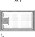
- Fig. 7 shows plan view of a vertical power MOS chip. In the case of the vertical power MOS chip, most of the chip surface is covered a source electrode 1. Further, a drain electrode is provided on the back surface of the power MOS chip.
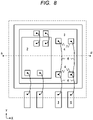
- FIG. 8 is a plan view of IPD in which control chip 2 is mounted on top of power MOS chip 3 (an encapsulant is transparent).
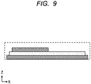
- FIG. 9 is a cross-sectional view along A-A' of FIG. 8 .
- a source pad 4 is provided on the source electrode of the power MOS chip 3, a lead 5 (source terminal) of the package and the source pad 4 are connected by a bonding wire 6.
- the drain electrode of the power MOS chip 3 is connected to a drain terminal of the package.
- Variation of the current results in breakdown of the power MOS chip and degradation of the performance.
- a semiconductor device includes a power MOS chip having a source electrode on a surface and a control chip mounted on a portion of the power MOS chip, wherein, viewing from a first outer edge of the power MOS chip extending in a first direction to the control chip, a first column bonding pad and a second column bonding pad are formed in a region of the source electrode where the control chip is not mounted, and wherein a distance between a second outer edge of the power MOS chip extending in a second direction and the first column bonding pad is longer than a distance between the second outer edge and the second column bonding pad.
- FIG. 1 is a plan view of an IPD 10 according to first embodiment.
- FIG. 1 is a transparent view of the encapsulant 14.
- IPD 10 has a control chip 11, a power MOS chip 12.
- the control chip 11 is mounted on top of the power MOS chip 12.
- Power MOS chip 12 is a vertical power MOSFET (or IGBT), there is a source electrode on the front surface and a drain electrode on the back surface.
- Bonding pads P1-P6 are installed on the surface of the power MOS chip 12.
- Bonding pads P1-P5 are source pads.
- Bonding pad P6 is a gate pad.
- Bonding pads P1 and P2 are connected to the lead (terminal) L1 by bonding wires W1 and W2.
- Bonding pads P3 and P4 are connected to the lead L2 by bonding wires W3 and W4.
- the drain electrode on the back surface of the power chip 12 is connected to the lead frame 13.
- the control chip 11 has bonding pads P7-P10.
- the bonding pad P7 is connected to the bonding pad P5 by a bonding wire W5.
- the bonding pad P8 is connected to the bonding pad P6 by a bonding wire W6.
- the bonding pad P9 is connected to the lead L3 by a bonding wire W7.
- the bonding pad P10 is connected to the lead L4 by a bonding wire W8.
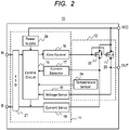
- FIG. 2 is a schematic diagram of the IPD 10.
- the power MOS chip 12 has a power MOSFET 23, a sense MOSFET 22, and a temperature sensor 24.
- Sense MOSFET 22 is a device for detecting the current flowing through the power MOSFET 23. Since these elements are generally used, detailed description thereof will be omitted.
- the control chip 11 includes a control circuit 15, a gate control circuit 16, a current detector 17, a voltage sense circuit 18, a current sense circuit 19, a power supply circuit 20 and an ESD protection circuit 21.
- the control circuit 15 and the gate control circuit 16 in response to an input signal from the outside (IN), generates a gate signal of the power MOSFET 23 and the sense MOSFET 22.
- Current detector 17 detects the current flowing through the source of the sense MOSFET 22.
- Voltage sense circuit 18 detects the source voltage of the power MOSFET 23 (output voltage).
- Current sense circuit 19 detects the current flowing through the sense MOSFET 22, and outputs the detection result from the output terminal IS.
- Bonding pad P8 is coupled to the output of the gate control circuit 16.
- the gate pad P6 is coupled to the gate of the power MOSFET 23 and sense MOSFET 22.
- Bonding pad P7 is coupled to the input of the current detector 17.
- Bonding pad P5 is coupled to the source of the sense MOSFET 22.
- the bonding pad P10 is coupled to an input of the control circuit 15.
- Bonding pad P9 is connected to the output of the current sense circuit 19. In FIG. 1 , a part of the connection between the control chip 11 and the power MOS chip 12 is omitted for simplifying.
- bonding pads P1 to P4 which are characteristics of the first embodiment, will be described.
- bonding pads P1 to P4 are formed in the region where the control chip 11 is not mounted in the power MOS chip 12.
- the bonding pads P1 and P2 are called as a first column bonding pad (C1)
- the bonding pads P3 and P4 are called as a second column bonding pad (C2).
- the first column bonding pad is formed inward from the outer edge of the power MOS chip 12 along the X-axis.
- a distance d1 from the outer edge of the power MOS chip 12 along the X-axis to the first column bonding pad is longer than a distance d2 from the outer edge of the power MOS chip 12 along the X-axis to the second column bonding pad.
- the bonding pads P3 and P4 have charge of a large area of the source electrode. Further, it can be said that the bonding pads P1 and P2 have charge of small area of the source electrode. This caused variations in the current flowing in the power MOSFET.
- the bonding pads P1 and P2 by forming the bonding pads P1 and P2 at a position away from the corner of the power MOS chip 12 than the prior art, and a position away from the bonding pads P3 and P4, the area of the source electrode that the bonding pads P1 and P2 have charge of is increased.
- the area of the source electrode which the bonding pads P1 and P2 have charge of is widened, the area of the source electrode which bonding pads P3 and P4 have charge of is narrowed. Therefore, compared to the prior art, it is possible to suppress variations in the current flowing through the power MOSFET.
- the bonding pads P1 to P4 are formed in two columns, and the number of bonding pads per column is two. However, it is not limited to this.
- the bonding pads may be arranged in three or more columns, and the number of bonding pads per column may be three or more.
- Fig. 3 shows plan view for three columns of bonding pads and three bonding pads per column.
- the bonding pads (source pads) P11 to P15, the bonding wires W9 to W13, and the lead L5 are added as compared with Fig. 1 .
- the first column bonding pad is formed inside the second column bonding pad, as the same as in FIG. 1 .
- the first column bonding pad is formed more inward than the second column bonding pad. Therefore, it is possible to suppress variations in the current flowing through the power MOSFET.
- FIG. 4 is a plan view of an IPD 10a according to second embodiment.
- the difference from first embodiment is that the control chip 11 is mounted near the central of the power MOS chip 12. More precisely, the control chip 11 is mounted on the X axis near the central of the power MOS chip 12.
- bonding pads (source pads) P16 to P19, bonding wires W14 to W 17, and leads L6 and L7 are added.
- Bonding pads P16 and P17 are connected to lead L6 by bonding wires W14 and W15.
- Bonding pads P18 and P19 are connected to lead L7 by bonding wires W16 and W17.
- Bonding pads P1-P4 are formed in the power MOS chip 12 in a first region where the control chip 11 is not mounted. Bonding pads P16-P19 are formed in the power MOS chip 12 in a second region where the control chip 11 is not mounted.
- the first region is the region between the first outer edge of the power MOS chip 12 along the Y-axis and the control chip 11.
- the second region is the region between the second outer edge of the power MOS chip 12 along the Y-axis and the control chip 11.
- the bonding pads P1 and P2 are the first column bonding pad
- the bonding pads P3 and P4 are the second column bonding pad.
- the bonding pads P18 and P19 are a first column (a third column in total) bonding pad (C3)
- the bonding pads P16 and P17 are a second column (a fourth column in total) bonding pad (C4).
- the third column bonding pad is formed in the same manner as the first column bonding pad, and the fourth column bonding pad is formed in the same manner as the second column bonding pad. That is, compared to the fourth column bonding pad, the third column bonding pad is formed inward from the outer edge of the power MOS chip 12 along the X-axis. In other words, the third and fourth column bonding pads and the first and second column bonding pads are formed in line symmetry with respect to the mounting point of the control chip 11.
- the second embodiment can suppress variations in the current flowing in the power MOSFET.
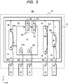
- FIG. 5 is a plan view of an IPD 10b according to third embodiment. Like second embodiment, bonding pads are also formed on the left side of the control chip 11.
- a first column (a third column in total) bonding pad (source pad) P22, the bonding wires W18 to W19, and the lead L8 are added to the second region.
- the first column bonding pad (C1) is composed of two bonding pads P1 and P2
- the second column bonding pad (C2) is composed of two bonding pads P3 and P4.
- the first column bonding pads is composed of one rectangular bonding pad P20
- the second column bonding pad is composed of one rectangular bonding pad P21.
- the third column bonding pad P22 is connected to the lead L8 by bonding wires W18 and W19.
- the first column bonding pad P20 is formed at a distance d1 from the outer edge of the power MOS chip 12 along the X-axis
- the second column bonding pad P21 is formed at a distance d2 from the outer edge (d1>d2).
- the third column bonding pad P22 is formed at a distance d3 from the outer edge. Where d1>d3>d2.
- the third column bonding pad P22 By forming the third column bonding pad P22 at a position away from the corners (upper left corner, lower left corner) of the power MOS chip 12, for the same reason as the first column bonding pad, it is possible to increase the area of the source electrode which the bonding pad P22 has charge of.
- the first and second column bonding pads are formed on the right side of the control chip 11, but only the bonding pad P22 is formed on the left side of the control chip 11. That is, although both the first and second column bonding pads can contribute to the source electrode near the upper right corner and the lower right corner of the power MOS chip 12, only the bonding pad P22 can contribute to the source electrode near the upper left corner and the lower left corner of the power MOS chip 12. Therefore, by setting d1>d3>d2, the area of the source electrode which the bonding pad P22 has charge of is increased, and the degree of contribution to the source electrode near the corner is increased.
- IPD 10b of the third embodiment can obtain the effects of first embodiment or more.
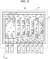
- FIG. 6 is a plan view of an IPD 10c according to fourth embodiment. The difference from first embodiment is that six column bonding pads C1 to C6 are formed on the right side of the control chip 11.
- the first and second column bonding pads (C1, C2) are the same as those in first embodiment.
- the third column bonding pad C3 is composed of bonding pads P23 and P24.
- the fourth column bonding pad C4 is composed of bonding pads P25 and P26.
- the fifth column bonding pad C5 is composed of bonding pads P27 and P28.
- the sixth column bonding pads C6 is composed of bonding pads P29 and P30.
- the third column bonding pad C3 is connected to the lead L9 by bonding wires W20 and W21.
- the fourth column bonding pad C4 is connected to the lead L10 by bonding wires W22 and W23.
- the fifth column bonding pad C5 is connected to the lead L11 by bonding wires W24 and W25.
- the sixth column bonding pad C6 is connected to the lead L12 by the bonding wires W26 and W27.
- the distances d1, d3, d5 from the outer edge of the power MOS chip 12 along the X-axis to the oddnumbered column bonding pads C1, C3, C5 are progressively shortened (d1>d3>d5).
- the distances d2, d4, and d6 from the outer edge of the power MOS chip 12 along the X-axis to the evennumbered column bonding pads C2, C4, and C6 gradually increase (d2 ⁇ d4 ⁇ d6). This is because the influence of the corners (upper right corner, lower right corner) of the power MOS chip 12 gradually decreases from the outer edge of the power MOS chip 12 along the X-axis to the control chip 11.
- the bonding pads may be arranged in six or more columns.
- the respective column bonding pads (C1 to C6) may be composed of three or more bonding pads, or may be composed of one rectangular bonding pad as in third embodiment.
- IPD 10c of the present fourth embodiment can obtain the effects of first embodiment or more.
Landscapes
- Metal-Oxide And Bipolar Metal-Oxide Semiconductor Integrated Circuits (AREA)
- Semiconductor Integrated Circuits (AREA)
- Wire Bonding (AREA)
Abstract
Description
- The present invention relates to semiconductor device, particularly semiconductor device having a power semiconductor device.
- In order to drive a load such as a motor, a heater, a lamp mounted on a vehicle and to perform voltage conversion, a power semiconductor element is used. As the power semiconductor device, a power MOSFET or an IGBT (Insulated Gate Bipolar Transistor) is used.
- In-vehicle semiconductor device, from the viewpoint of functional safety, it is desirable to equip a failure detecting function and a protective function. Therefore, a function for detecting abnormal conditions such as overcurrent or overheating of the power MOSFET and protecting the power MOSFET and a function for outputting self-diagnosis data to monitor the output status of the power MOSFET are installed in semiconductor device using the power MOSFET (or IGBT).
- A semiconductor chip (also called as a power MOS chip) mounting a power MOSFET, and a semiconductor chip (also called as a control chip) controlling the power MOS chip and mounting the protective function and the self-diagnosis output function are composed of separated semiconductor chips. Recently, for miniaturization and cost reduction of products, a product called IPD (Intelligent Power Device) in which the power MOS chip and the control chip are mounted in one package is used.
-
Patent Document 1, a technique for mounting a plurality of power MOS chips and a semiconductor chip including a drive circuit and a control circuit of the power MOSFET in one package is disclosed. - [Patent Document 1]
Japanese Unexamined Patent Application Publication No. 2008-17620 - In
Patent Document 1, a plurality of chips is arranged on a plane, but there is also a stack structure IPD in which the control chip is mounted on the power MOS chip.FIGS. 7 to 9 are used to explain.Fig. 7 shows plan view of a vertical power MOS chip. In the case of the vertical power MOS chip, most of the chip surface is covered asource electrode 1. Further, a drain electrode is provided on the back surface of the power MOS chip.FIG. 8 is a plan view of IPD in whichcontrol chip 2 is mounted on top of power MOS chip 3 (an encapsulant is transparent).FIG. 9 is a cross-sectional view along A-A' ofFIG. 8 . Asource pad 4 is provided on the source electrode of thepower MOS chip 3, a lead 5 (source terminal) of the package and thesource pad 4 are connected by abonding wire 6. The drain electrode of thepower MOS chip 3 is connected to a drain terminal of the package. When mounting thecontrol chip 2 on thepower MOS chip 3, a region for providing thesource pad 4 is limited. This is because thesource pad 4 must be provided in a region where thecontrol chip 2 is not disposed in the source electrode of thepower MOS chip 3. In this case, a problem that a current flowing is varied depending on a location in thepower MOS chip 3 is occurred. This is because more current flows through a transistor formed near thesource pad 4, and less current flows through a transistor formed at a position away from thesource pad 4. - Variation of the current results in breakdown of the power MOS chip and degradation of the performance. The place where more current flows is likely to occur breakdown, the place where less current flows is hard to contribute to the reduction of the on-resistance.
- Other objects and novel features will become apparent from the description of the specification and drawings.
- A semiconductor device according to an embodiment includes a power MOS chip having a source electrode on a surface and a control chip mounted on a portion of the power MOS chip, wherein, viewing from a first outer edge of the power MOS chip extending in a first direction to the control chip, a first column bonding pad and a second column bonding pad are formed in a region of the source electrode where the control chip is not mounted, and wherein a distance between a second outer edge of the power MOS chip extending in a second direction and the first column bonding pad is longer than a distance between the second outer edge and the second column bonding pad.
- Semiconductor device according to an embodiment, it is possible to reduce the variation of the current flowing through the power MOSFET.
-
-
FIG. 1 is a plan view of a semiconductor device according to first embodiment. -
FIG. 2 is a schematic diagram of the semiconductor device according to first embodiment. -
FIG. 3 is a plan view of semiconductor device according to first embodiment. -
FIG. 4 is a plan view of semiconductor device according to second embodiment. -
FIG. 5 is a plan view of semiconductor device according to third embodiment. -
FIG. 6 is a plan view of semiconductor device according to fourth embodiment. -
FIG. 7 shows plan view of the power MOS chip. -
FIG. 8 shows plan view of the conventional semiconductor device. -
FIG. 9 shows cross-sectional view of the conventional semiconductor device. - Hereinafter, a semiconductor device according to an embodiment will be described in detail by referring to the drawings. In the specification and the drawings, the same or corresponding form elements are denoted by the same reference numerals, and a repetitive description thereof is omitted. In the drawings, for convenience of description, the configuration may be omitted or simplified. Also, at least some of the embodiments may be arbitrarily combined with each other.
-
FIG. 1 is a plan view of anIPD 10 according to first embodiment. For ease of understanding,FIG. 1 is a transparent view of theencapsulant 14. As shown inFIG. 1 ,IPD 10 has acontrol chip 11, apower MOS chip 12. Thecontrol chip 11 is mounted on top of thepower MOS chip 12. -
Power MOS chip 12 is a vertical power MOSFET (or IGBT), there is a source electrode on the front surface and a drain electrode on the back surface. Bonding pads P1-P6 are installed on the surface of thepower MOS chip 12. Bonding pads P1-P5 are source pads. Bonding pad P6 is a gate pad. Bonding pads P1 and P2 are connected to the lead (terminal) L1 by bonding wires W1 and W2. Bonding pads P3 and P4 are connected to the lead L2 by bonding wires W3 and W4. The drain electrode on the back surface of thepower chip 12 is connected to thelead frame 13. - The
control chip 11 has bonding pads P7-P10. The bonding pad P7 is connected to the bonding pad P5 by a bonding wire W5. The bonding pad P8 is connected to the bonding pad P6 by a bonding wire W6. The bonding pad P9 is connected to the lead L3 by a bonding wire W7. The bonding pad P10 is connected to the lead L4 by a bonding wire W8. -
FIG. 2 is a schematic diagram of theIPD 10. Thepower MOS chip 12 has apower MOSFET 23, asense MOSFET 22, and atemperature sensor 24.Sense MOSFET 22 is a device for detecting the current flowing through thepower MOSFET 23. Since these elements are generally used, detailed description thereof will be omitted. - The
control chip 11 includes acontrol circuit 15, agate control circuit 16, acurrent detector 17, avoltage sense circuit 18, acurrent sense circuit 19, apower supply circuit 20 and anESD protection circuit 21. Thecontrol circuit 15 and thegate control circuit 16, in response to an input signal from the outside (IN), generates a gate signal of thepower MOSFET 23 and thesense MOSFET 22.Current detector 17 detects the current flowing through the source of thesense MOSFET 22.Voltage sense circuit 18 detects the source voltage of the power MOSFET 23 (output voltage).Control circuit 15, with reference to the output results of thecurrent detector 17, thevoltage sense circuit 18 andtemperature sensor 24, generates the gate signal.Current sense circuit 19 detects the current flowing through thesense MOSFET 22, and outputs the detection result from the output terminal IS. - Returning to
FIG. 1 , description will be made again. Bonding pad P8 is coupled to the output of thegate control circuit 16. The gate pad P6 is coupled to the gate of thepower MOSFET 23 andsense MOSFET 22. Bonding pad P7 is coupled to the input of thecurrent detector 17. Bonding pad P5 is coupled to the source of thesense MOSFET 22. The bonding pad P10 is coupled to an input of thecontrol circuit 15. Bonding pad P9 is connected to the output of thecurrent sense circuit 19. InFIG. 1 , a part of the connection between thecontrol chip 11 and thepower MOS chip 12 is omitted for simplifying. - Next, the bonding pads P1 to P4, which are characteristics of the first embodiment, will be described. As shown in
FIG. 1 , bonding pads P1 to P4 are formed in the region where thecontrol chip 11 is not mounted in thepower MOS chip 12. When counted from the outer edge of thepower MOS chip 12 along the Y-axis to thecontrol chip 11 side, the bonding pads P1 and P2 are called as a first column bonding pad (C1), the bonding pads P3 and P4 are called as a second column bonding pad (C2). Compared to the second column bonding pad, the first column bonding pad is formed inward from the outer edge of thepower MOS chip 12 along the X-axis. That is, a distance d1 from the outer edge of thepower MOS chip 12 along the X-axis to the first column bonding pad is longer than a distance d2 from the outer edge of thepower MOS chip 12 along the X-axis to the second column bonding pad. - Compared to the bonding pads P1 and P2, a contribution of the bonding pads P3 and P4 to the current flowing in the power MOSFET formed beneath the
control chip 11 is inevitably increased. In other words, it can be said that the bonding pads P3 and P4 have charge of a large area of the source electrode. Further, it can be said that the bonding pads P1 and P2 have charge of small area of the source electrode. This caused variations in the current flowing in the power MOSFET. In the first embodiment, by forming the bonding pads P1 and P2 at a position away from the corner of thepower MOS chip 12 than the prior art, and a position away from the bonding pads P3 and P4, the area of the source electrode that the bonding pads P1 and P2 have charge of is increased. By the area of the source electrode which the bonding pads P1 and P2 have charge of is widened, the area of the source electrode which bonding pads P3 and P4 have charge of is narrowed. Therefore, compared to the prior art, it is possible to suppress variations in the current flowing through the power MOSFET. - In
FIG. 1 , the bonding pads P1 to P4 are formed in two columns, and the number of bonding pads per column is two. However, it is not limited to this. The bonding pads may be arranged in three or more columns, and the number of bonding pads per column may be three or more.Fig. 3 shows plan view for three columns of bonding pads and three bonding pads per column. InFig. 3 , the bonding pads (source pads) P11 to P15, the bonding wires W9 to W13, and the lead L5 are added as compared withFig. 1 . The first column bonding pad is formed inside the second column bonding pad, as the same as inFIG. 1 . By increasing the number of bonding pads, it is possible to further suppress the variation of the current flowing through the power MOSFET. - As described above, in
IPD 10 of first embodiment, the first column bonding pad is formed more inward than the second column bonding pad. Thus, it is possible to suppress variations in the current flowing through the power MOSFET. -
FIG. 4 is a plan view of anIPD 10a according to second embodiment. The difference from first embodiment is that thecontrol chip 11 is mounted near the central of thepower MOS chip 12. More precisely, thecontrol chip 11 is mounted on the X axis near the central of thepower MOS chip 12. - In
FIG. 4 , as compared withFIG. 1 , bonding pads (source pads) P16 to P19, bonding wires W14 toW 17, and leads L6 and L7 are added. Bonding pads P16 and P17 are connected to lead L6 by bonding wires W14 and W15. Bonding pads P18 and P19 are connected to lead L7 by bonding wires W16 and W17. - Bonding pads P1-P4 are formed in the
power MOS chip 12 in a first region where thecontrol chip 11 is not mounted. Bonding pads P16-P19 are formed in thepower MOS chip 12 in a second region where thecontrol chip 11 is not mounted. The first region is the region between the first outer edge of thepower MOS chip 12 along the Y-axis and thecontrol chip 11. The second region is the region between the second outer edge of thepower MOS chip 12 along the Y-axis and thecontrol chip 11. - Similar to first embodiment, when counted from the first outer edge of the
power MOS chip 12 along the Y-axis to thecontrol chip 11 side, the bonding pads P1 and P2 are the first column bonding pad, the bonding pads P3 and P4 are the second column bonding pad. Similarly, when counting from the second outer edge of thepower MOS chip 12 along the Y-axis to thecontrol chip 11 side, the bonding pads P18 and P19 are a first column (a third column in total) bonding pad (C3), and the bonding pads P16 and P17 are a second column (a fourth column in total) bonding pad (C4). The third column bonding pad is formed in the same manner as the first column bonding pad, and the fourth column bonding pad is formed in the same manner as the second column bonding pad. That is, compared to the fourth column bonding pad, the third column bonding pad is formed inward from the outer edge of thepower MOS chip 12 along the X-axis. In other words, the third and fourth column bonding pads and the first and second column bonding pads are formed in line symmetry with respect to the mounting point of thecontrol chip 11. - When the
control chip 11 is mounted near the center of thepower MOS chip 12, the second embodiment can suppress variations in the current flowing in the power MOSFET. - As described above, in
IPD 10a of second embodiment, the same effects as those of first embodiment can be obtained. -
FIG. 5 is a plan view of anIPD 10b according to third embodiment. Like second embodiment, bonding pads are also formed on the left side of thecontrol chip 11. - In
FIG. 5 , a first column (a third column in total) bonding pad (source pad) P22, the bonding wires W18 to W19, and the lead L8 are added to the second region. In first embodiment, the first column bonding pad (C1) is composed of two bonding pads P1 and P2, the second column bonding pad (C2) is composed of two bonding pads P3 and P4. InFIG. 5 , the first column bonding pads is composed of one rectangular bonding pad P20, and the second column bonding pad is composed of one rectangular bonding pad P21. Then, the third column bonding pad P22 is connected to the lead L8 by bonding wires W18 and W19. - Similar to first embodiment, the first column bonding pad P20 is formed at a distance d1 from the outer edge of the
power MOS chip 12 along the X-axis, the second column bonding pad P21 is formed at a distance d2 from the outer edge (d1>d2). The third column bonding pad P22 is formed at a distance d3 from the outer edge. Where d1>d3>d2. - By forming the third column bonding pad P22 at a position away from the corners (upper left corner, lower left corner) of the
power MOS chip 12, for the same reason as the first column bonding pad, it is possible to increase the area of the source electrode which the bonding pad P22 has charge of. However, the first and second column bonding pads are formed on the right side of thecontrol chip 11, but only the bonding pad P22 is formed on the left side of thecontrol chip 11. That is, although both the first and second column bonding pads can contribute to the source electrode near the upper right corner and the lower right corner of thepower MOS chip 12, only the bonding pad P22 can contribute to the source electrode near the upper left corner and the lower left corner of thepower MOS chip 12. Therefore, by setting d1>d3>d2, the area of the source electrode which the bonding pad P22 has charge of is increased, and the degree of contribution to the source electrode near the corner is increased. - As described above,
IPD 10b of the third embodiment can obtain the effects of first embodiment or more. -
FIG. 6 is a plan view of anIPD 10c according to fourth embodiment. The difference from first embodiment is that six column bonding pads C1 to C6 are formed on the right side of thecontrol chip 11. - The first and second column bonding pads (C1, C2) are the same as those in first embodiment. The third column bonding pad C3 is composed of bonding pads P23 and P24. The fourth column bonding pad C4 is composed of bonding pads P25 and P26. The fifth column bonding pad C5 is composed of bonding pads P27 and P28. The sixth column bonding pads C6 is composed of bonding pads P29 and P30.
- The third column bonding pad C3 is connected to the lead L9 by bonding wires W20 and W21. The fourth column bonding pad C4 is connected to the lead L10 by bonding wires W22 and W23. The fifth column bonding pad C5 is connected to the lead L11 by bonding wires W24 and W25. The sixth column bonding pad C6 is connected to the lead L12 by the bonding wires W26 and W27.
- As shown in
FIG. 6 , the distances d1, d3, d5 from the outer edge of thepower MOS chip 12 along the X-axis to the oddnumbered column bonding pads C1, C3, C5 are progressively shortened (d1>d3>d5). The distances d2, d4, and d6 from the outer edge of thepower MOS chip 12 along the X-axis to the evennumbered column bonding pads C2, C4, and C6 gradually increase (d2<d4<d6). This is because the influence of the corners (upper right corner, lower right corner) of thepower MOS chip 12 gradually decreases from the outer edge of thepower MOS chip 12 along the X-axis to thecontrol chip 11. - In the fourth embodiment, when forming the three or more column bonding pads, it is possible to suppress variations of the current flowing in the power MOSFET.
- The bonding pads may be arranged in six or more columns. In addition, the respective column bonding pads (C1 to C6) may be composed of three or more bonding pads, or may be composed of one rectangular bonding pad as in third embodiment.
- As described above,
IPD 10c of the present fourth embodiment can obtain the effects of first embodiment or more. - It should be noted that the present invention is not limited to the above-mentioned embodiments, and various modifications can be made without departing from the gist thereof.
Claims (9)
- A semiconductor device comprising:a power MOS chip having a source electrode on a surface; anda control chip mounted on a portion of the power MOS chip, wherein, viewing from a first outer edge of the power MOS chip extending in a first direction to the control chip, a first column bonding pad and a second column bonding pad are formed in a region of the source electrode where the control chip is not mounted, andwherein a distance between a second outer edge of the power MOS chip extending in a second direction and the first column bonding pad is longer than a distance between the second outer edge and the second column bonding pad.
- The semiconductor device according to claim 1,wherein the power MOS chip has a first and second bonding pads,wherein the control chip has third and fourth bonding pads,wherein the first bonding pad is coupled to the third bonding pad by a first bonding wire, andwherein the second bonding pad is coupled to the fourth bonding pad by a second bonding wire.
- The semiconductor device according to claim 1 or 2,wherein the power MOS chip has a first and second regions of the source electrode where the control chip is not mounted,wherein the first region is a region between the first outer edge and the control chip,wherein the second region is a region between a third outer edge of the power MOS chip extending in the first direction and the control chip,wherein the first and second column bonding pads are formed in the first region, andwherein a third column bonding pad is further formed in the second region.
- The semiconductor device according to claim 3,wherein a fourth column bonding pad is further formed in the second region, andwherein the first and second column bonding pads and the third and fourth column bonding pads are formed in line symmetry with respect to a mounting point of the control chip.
- The semiconductor device according to claim 1 or 2, wherein each of the first and second column bonding pads is composed of a plurality of bonding pads.
- The semiconductor device according to claim 3, wherein each of the first to third column bonding pads is formed of a rectangular bonding pad.
- The semiconductor device according to claim 3, wherein a distance between the second outer edge and the third column bonding pad is shorter than the distance between the second outer edge and the first column bonding pad, and is longer than the distance between the second outer edge and the second column bonding pad.
- The semiconductor device according to claim 1 or 2,wherein a plurality of column bonding pads is formed in the region of the source electrode where the control chip is not mounted,wherein, viewing from the first outer edge to the control chip, distances between odd column bonding pads and the second outer edge are gradually decreased, andwherein, viewing from the first outer edge to the control chip, distances between even column bonding pads and the second outer edge are gradually increased.
- The semiconductor device according to any one of claims 1 to 8, wherein the semiconductor device is an IPD (Intelligent Power Device) .
Applications Claiming Priority (1)
| Application Number | Priority Date | Filing Date | Title |
|---|---|---|---|
| US17/082,766 US11289437B1 (en) | 2020-10-28 | 2020-10-28 | Semiconductor device |
Publications (1)
| Publication Number | Publication Date |
|---|---|
| EP3993034A1 true EP3993034A1 (en) | 2022-05-04 |
Family
ID=78592397
Family Applications (1)
| Application Number | Title | Priority Date | Filing Date |
|---|---|---|---|
| EP21203088.6A Pending EP3993034A1 (en) | 2020-10-28 | 2021-10-18 | Semiconductor device |
Country Status (4)
| Country | Link |
|---|---|
| US (1) | US11289437B1 (en) |
| EP (1) | EP3993034A1 (en) |
| JP (1) | JP7611792B2 (en) |
| CN (1) | CN114497014A (en) |
Citations (5)
| Publication number | Priority date | Publication date | Assignee | Title |
|---|---|---|---|---|
| US6184585B1 (en) * | 1997-11-13 | 2001-02-06 | International Rectifier Corp. | Co-packaged MOS-gated device and control integrated circuit |
| US20020163040A1 (en) * | 2001-05-02 | 2002-11-07 | International Rectifier Corp. | Power mosfet with integrated drivers in a common package |
| US20030102489A1 (en) * | 1999-09-13 | 2003-06-05 | Nam Shi-Baek | Power device having multi-chip package structure |
| JP2006066704A (en) * | 2004-08-27 | 2006-03-09 | Toyota Motor Corp | Semiconductor device |
| JP2008017620A (en) | 2006-07-06 | 2008-01-24 | Renesas Technology Corp | Semiconductor device |
Family Cites Families (13)
| Publication number | Priority date | Publication date | Assignee | Title |
|---|---|---|---|---|
| JP3383451B2 (en) * | 1995-01-30 | 2003-03-04 | 株式会社東芝 | Semiconductor device |
| JPH09266226A (en) * | 1996-03-28 | 1997-10-07 | Toshiba Corp | Semiconductor device and manufacturing method thereof |
| US5767567A (en) * | 1996-09-10 | 1998-06-16 | Magemos Corporation | Design of device layout for integration with power mosfet packaging to achieve better lead wire connections and lower on resistance |
| JP2005317830A (en) * | 2004-04-30 | 2005-11-10 | Elpida Memory Inc | Semiconductor device, multichip package, and wire bonding method |
| EP1909326A4 (en) * | 2005-07-26 | 2009-05-06 | Panasonic Corp | SEMICONDUCTOR ELEMENT AND ELECTRICAL DEVICE |
| US7291869B2 (en) * | 2006-02-06 | 2007-11-06 | Infieon Technologies A.G. | Electronic module with stacked semiconductors |
| JP5054359B2 (en) * | 2006-12-01 | 2012-10-24 | パナソニック株式会社 | Semiconductor integrated circuit and manufacturing method thereof |
| JP4830877B2 (en) * | 2007-01-31 | 2011-12-07 | トヨタ自動車株式会社 | Manufacturing method of semiconductor device |
| US20090294977A1 (en) * | 2008-06-02 | 2009-12-03 | Che-Yuan Jao | Semiconductor die and bond pad arrangement method thereof |
| JP5405785B2 (en) * | 2008-09-19 | 2014-02-05 | ルネサスエレクトロニクス株式会社 | Semiconductor device |
| JP2012104707A (en) * | 2010-11-11 | 2012-05-31 | Elpida Memory Inc | Semiconductor package |
| JP6420617B2 (en) * | 2014-09-30 | 2018-11-07 | ルネサスエレクトロニクス株式会社 | Semiconductor device |
| KR102150111B1 (en) * | 2014-10-01 | 2020-08-31 | 에스케이하이닉스 주식회사 | semiconductor stack package |
-
2020
- 2020-10-28 US US17/082,766 patent/US11289437B1/en active Active
-
2021
- 2021-09-17 JP JP2021151963A patent/JP7611792B2/en active Active
- 2021-09-26 CN CN202111128076.9A patent/CN114497014A/en active Pending
- 2021-10-18 EP EP21203088.6A patent/EP3993034A1/en active Pending
Patent Citations (5)
| Publication number | Priority date | Publication date | Assignee | Title |
|---|---|---|---|---|
| US6184585B1 (en) * | 1997-11-13 | 2001-02-06 | International Rectifier Corp. | Co-packaged MOS-gated device and control integrated circuit |
| US20030102489A1 (en) * | 1999-09-13 | 2003-06-05 | Nam Shi-Baek | Power device having multi-chip package structure |
| US20020163040A1 (en) * | 2001-05-02 | 2002-11-07 | International Rectifier Corp. | Power mosfet with integrated drivers in a common package |
| JP2006066704A (en) * | 2004-08-27 | 2006-03-09 | Toyota Motor Corp | Semiconductor device |
| JP2008017620A (en) | 2006-07-06 | 2008-01-24 | Renesas Technology Corp | Semiconductor device |
Also Published As
| Publication number | Publication date |
|---|---|
| US11289437B1 (en) | 2022-03-29 |
| CN114497014A (en) | 2022-05-13 |
| JP7611792B2 (en) | 2025-01-10 |
| JP2022071826A (en) | 2022-05-16 |
Similar Documents
| Publication | Publication Date | Title |
|---|---|---|
| JP7531444B2 (en) | Semiconductor Device | |
| EP3660899B1 (en) | Semiconductor module | |
| US7755187B2 (en) | Load driving device | |
| US20170110395A1 (en) | Semiconductor device | |
| US10256640B2 (en) | Semiconductor device | |
| EP3832862A1 (en) | Power conversion device | |
| US12615787B2 (en) | Isolator including electrically floating intermediate electrode portion | |
| US12581992B2 (en) | Insulation module and gate driver | |
| US20200211934A1 (en) | Leadframe for multichip devices with thinned die pad portions | |
| JP2002153079A (en) | Semiconductor device | |
| JP7611792B2 (en) | Semiconductor Device | |
| US20200211954A1 (en) | Semiconductor module | |
| US20160027400A1 (en) | Display panel | |
| US11749620B2 (en) | Semiconductor module | |
| US11848245B2 (en) | Power semiconductor apparatus | |
| US12355436B2 (en) | Gate driver, insulation module, low-voltage circuit unit, and high-voltage circuit unit | |
| US12635588B2 (en) | Semiconductor device and circuit board | |
| US20250316657A1 (en) | Semiconductor device | |
| US20240186302A1 (en) | Semiconductor device and circuit board | |
| US7989964B2 (en) | Semiconductor integrated circuit | |
| EP4576212A1 (en) | Semiconductor dc breaker and semiconductor module | |
| US12154905B2 (en) | Arrayed switch circuit, switching element and system chip package structure | |
| JP7862368B2 (en) | Isolators, isolation modules, and gate drivers | |
| US12532753B2 (en) | Switching device, semiconductor device, and switching device manufacturing method | |
| US20230395582A1 (en) | Semiconductor device |
Legal Events
| Date | Code | Title | Description |
|---|---|---|---|
| PUAI | Public reference made under article 153(3) epc to a published international application that has entered the european phase |
Free format text: ORIGINAL CODE: 0009012 |
|
| STAA | Information on the status of an ep patent application or granted ep patent |
Free format text: STATUS: THE APPLICATION HAS BEEN PUBLISHED |
|
| AK | Designated contracting states |
Kind code of ref document: A1 Designated state(s): AL AT BE BG CH CY CZ DE DK EE ES FI FR GB GR HR HU IE IS IT LI LT LU LV MC MK MT NL NO PL PT RO RS SE SI SK SM TR |
|
| STAA | Information on the status of an ep patent application or granted ep patent |
Free format text: STATUS: REQUEST FOR EXAMINATION WAS MADE |
|
| 17P | Request for examination filed |
Effective date: 20221021 |
|
| RBV | Designated contracting states (corrected) |
Designated state(s): AL AT BE BG CH CY CZ DE DK EE ES FI FR GB GR HR HU IE IS IT LI LT LU LV MC MK MT NL NO PL PT RO RS SE SI SK SM TR |