EP3989361A1 - Antenna manufacturing method and antenna device - Google Patents
Antenna manufacturing method and antenna device Download PDFInfo
- Publication number
- EP3989361A1 EP3989361A1 EP19934581.0A EP19934581A EP3989361A1 EP 3989361 A1 EP3989361 A1 EP 3989361A1 EP 19934581 A EP19934581 A EP 19934581A EP 3989361 A1 EP3989361 A1 EP 3989361A1
- Authority
- EP
- European Patent Office
- Prior art keywords
- ground plane
- dielectric substrate
- conductor ground
- conductor
- antenna
- Prior art date
- Legal status (The legal status is an assumption and is not a legal conclusion. Google has not performed a legal analysis and makes no representation as to the accuracy of the status listed.)
- Pending
Links
Images















Classifications
-
- H—ELECTRICITY
- H01—ELECTRIC ELEMENTS
- H01Q—ANTENNAS, i.e. RADIO AERIALS
- H01Q9/00—Electrically-short antennas having dimensions not more than twice the operating wavelength and consisting of conductive active radiating elements
- H01Q9/04—Resonant antennas
- H01Q9/0407—Substantially flat resonant element parallel to ground plane, e.g. patch antenna
-
- H—ELECTRICITY
- H01—ELECTRIC ELEMENTS
- H01Q—ANTENNAS, i.e. RADIO AERIALS
- H01Q1/00—Details of, or arrangements associated with, antennas
- H01Q1/42—Housings not intimately mechanically associated with radiating elements, e.g. radome
-
- H—ELECTRICITY
- H01—ELECTRIC ELEMENTS
- H01Q—ANTENNAS, i.e. RADIO AERIALS
- H01Q1/00—Details of, or arrangements associated with, antennas
- H01Q1/12—Supports; Mounting means
- H01Q1/22—Supports; Mounting means by structural association with other equipment or articles
- H01Q1/2283—Supports; Mounting means by structural association with other equipment or articles mounted in or on the surface of a semiconductor substrate as a chip-type antenna or integrated with other components into an IC package
-
- H—ELECTRICITY
- H01—ELECTRIC ELEMENTS
- H01Q—ANTENNAS, i.e. RADIO AERIALS
- H01Q1/00—Details of, or arrangements associated with, antennas
- H01Q1/36—Structural form of radiating elements, e.g. cone, spiral, umbrella; Particular materials used therewith
- H01Q1/38—Structural form of radiating elements, e.g. cone, spiral, umbrella; Particular materials used therewith formed by a conductive layer on an insulating support
-
- H—ELECTRICITY
- H01—ELECTRIC ELEMENTS
- H01Q—ANTENNAS, i.e. RADIO AERIALS
- H01Q21/00—Antenna arrays or systems
- H01Q21/0006—Particular feeding systems
- H01Q21/0025—Modular arrays
-
- H—ELECTRICITY
- H01—ELECTRIC ELEMENTS
- H01Q—ANTENNAS, i.e. RADIO AERIALS
- H01Q21/00—Antenna arrays or systems
- H01Q21/0087—Apparatus or processes specially adapted for manufacturing antenna arrays
-
- H—ELECTRICITY
- H01—ELECTRIC ELEMENTS
- H01Q—ANTENNAS, i.e. RADIO AERIALS
- H01Q21/00—Antenna arrays or systems
- H01Q21/06—Arrays of individually energised antenna units similarly polarised and spaced apart
- H01Q21/061—Two dimensional planar arrays
- H01Q21/065—Patch antenna array
-
- H—ELECTRICITY
- H01—ELECTRIC ELEMENTS
- H01Q—ANTENNAS, i.e. RADIO AERIALS
- H01Q9/00—Electrically-short antennas having dimensions not more than twice the operating wavelength and consisting of conductive active radiating elements
- H01Q9/04—Resonant antennas
- H01Q9/0407—Substantially flat resonant element parallel to ground plane, e.g. patch antenna
- H01Q9/0414—Substantially flat resonant element parallel to ground plane, e.g. patch antenna in a stacked or folded configuration
-
- H—ELECTRICITY
- H01—ELECTRIC ELEMENTS
- H01Q—ANTENNAS, i.e. RADIO AERIALS
- H01Q9/00—Electrically-short antennas having dimensions not more than twice the operating wavelength and consisting of conductive active radiating elements
- H01Q9/04—Resonant antennas
- H01Q9/0407—Substantially flat resonant element parallel to ground plane, e.g. patch antenna
- H01Q9/0421—Substantially flat resonant element parallel to ground plane, e.g. patch antenna with a shorting wall or a shorting pin at one end of the element
-
- H—ELECTRICITY
- H01—ELECTRIC ELEMENTS
- H01Q—ANTENNAS, i.e. RADIO AERIALS
- H01Q9/00—Electrically-short antennas having dimensions not more than twice the operating wavelength and consisting of conductive active radiating elements
- H01Q9/04—Resonant antennas
- H01Q9/0407—Substantially flat resonant element parallel to ground plane, e.g. patch antenna
- H01Q9/045—Substantially flat resonant element parallel to ground plane, e.g. patch antenna with particular feeding means
- H01Q9/0457—Substantially flat resonant element parallel to ground plane, e.g. patch antenna with particular feeding means electromagnetically coupled to the feed line
-
- H—ELECTRICITY
- H01—ELECTRIC ELEMENTS
- H01Q—ANTENNAS, i.e. RADIO AERIALS
- H01Q21/00—Antenna arrays or systems
- H01Q21/06—Arrays of individually energised antenna units similarly polarised and spaced apart
Definitions
- the present disclosure relates to an antenna manufacturing method and an antenna device.
- an array antenna device In order to perform wireless communication in a wide angle even when radio waves are extremely weak, an array antenna device is demanded to have a high gain and a low axial ratio when performing beam scanning in a wide angle direction.
- the wide angle direction indicates a direction of a zenith angle ⁇ 60 degrees or more when the antenna is disposed horizontally with respect to the ground.
- the amplitude difference between a vertically polarized wave and a horizontally polarized wave in the wide angle direction is a factor tor causing the degradation of the axial ratio when beam scanning is performed in the wide angle direction.
- Patent Literature 1 discloses an antenna used as an antenna element of an array antenna.
- the antenna includes a first dielectric substrate, a second dielectric substrate, and a cylindrical member.
- the first dielectric substrate has a circular feed conductor on its front side, and a ground conductor on its back side.
- the second dielectric substrate has a back side facing the front side of the first dielectric substrate, and has a circular parasitic conductor formed on its front side.
- the cylindrical member is provided around a space defined by bonding a peripheral edge of the parasitic conductor and a peripheral edge of the feed conductor, and is made of dielectric material or conductive material.
- the space defined by bonding the peripheral edge of the parasitic conductor and the peripheral edge of the feed conductor by the cylindrical member is hollow, so that the equivalent dielectric constant of the dielectric substrates decreases.
- the amplitude difference between the vertically polarized wave and the horizontally polarized wave in the wide angle direction varies with a variation in the equivalent dielectric constant of the dielectric substrates.
- the antenna disclosed in Patent Literature 1 can adjust the amplitude difference between the vertically polarized wave and the horizontally polarized wave in the wide angle direction by varying the equivalent dielectric constant of the dielectric substrates by the hollow structure.
- Patent Literature 1 JP 2000-138525 A
- a conventional antenna represented by Patent Literature 1 is produced by performing hot pressing in a state where a plurality of dielectric substrates overlap each other. For example, hot pressing is performed in a state where the cylindrical member is provided on a substrate formed of a thermosetting dielectric material, and the first dielectric substrate and the second dielectric substrate are disposed so as to sandwich the substrate from both sides.
- the heated and melted dielectric material of the substrate flows through a gap between the first dielectric substrate and the second dielectric substrate, the gap is filled with this material, and it is cured in the gap.
- the periphery of the cylindrical member is filled with the dielectric material, but the space surrounded by the cylindrical member has no filling material and a portion corresponding to the opening of the cylindrical member is not supported by the filling material, and thus, a hollow structure is formed.
- the present disclosure addresses the above problems, and an object thereof is to obtain an antenna manufacturing method and an antenna device capable of preventing deformation of an antenna.
- An antenna manufacturing method is a method for manufacturing an antenna device including: a first dielectric substrate provided with a first conductor ground plane; a second dielectric substrate provided with a second conductor ground plane on a first side and a third conductor ground plane on a second side opposite to the first side; and a third dielectric substrate provided with a fourth conductor ground plane.
- This antenna manufacturing method includes: forming a through hole in the second dielectric substrate, the through hole penetrating from the second conductor ground plane to the third conductor ground plane; forming a patch antenna on the first conductor ground plane at a position to be faced by the through hole when the first dielectric substrate is bonded to the second dielectric substrate; and in a state in which the through hole and the patch antenna are arranged to face each other, bonding the first conductor ground plane of the first dielectric substrate and the second conductor ground plane of the second dielectric substrate by a first solder, and bonding the third conductor ground plane of the second dielectric substrate and the fourth conductor ground plane of the third dielectric substrate by a second solder.
- the first conductor ground plane provided on the first dielectric substrate and provided with the patch antenna and the second conductor ground plane provided on the first side of the second dielectric substrate having the through hole are bonded by the first solder in a state where the through hole and the patch antenna are arranged to face each other, and the third conductor ground plane provided on the second side of the second dielectric substrate and the fourth conductor ground plane provided on the third dielectric substrate are bonded by the second solder. Since the dielectric substrates are bonded using solder, a stress generated inside the dielectric substrates can be minimized as compared with bonding by hot pressing, so that deformation of the antenna can be prevented.
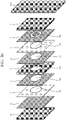
- FIG. 1 is a longitudinal sectional view illustrating a configuration of an antenna device according to the first embodiment.
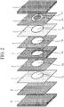
- FIG. 2 is an exploded perspective view illustrating the configuration of the antenna device illustrated in FIG. 1 .
- the antenna device according to the first embodiment includes a dielectric substrate 1, a conductor ground plane 2, solder 3, a conductor ground plane 4, a dielectric substrate 5, a conductor ground plane 6, solder 7, a conductor ground plane 8, and a dielectric substrate 9.
- a hollow structure 10 for adjusting an equivalent dielectric constant of the dielectric substrate is provided, and a patch antenna 11 faces the hollow structure 10.
- the dielectric substrate 1 is a first dielectric substrate having the conductor ground plane 2.
- the conductor ground plane 2 is a first conductor ground plane provided on the entire back side of the dielectric substrate 1, and is provided with the patch antenna 11.
- the patch antenna 11 is a first patch antenna formed in a circular shape, and is formed on the conductor ground plane 2 by providing a conductor removed portion 2a in the conductor ground plane 2 as illustrated in FIG. 2 .
- the conductor removed portion 2a is a portion formed by removing the conductor from the conductor ground plane 2 along the outer shape of the patch antenna 11.
- the conductor removed portion 2a is an annular portion formed by removing the conductor from the conductor ground plane 2 as illustrated in FIG. 2 .
- the patch antenna 11 is not limited to one having a circular shape, and it may have, for example, a polygonal shape such as a triangular shape or a quadrangular shape.
- the dielectric substrate 5 is a second dielectric substrate including the conductor ground plane 4 and the conductor ground plane 6.
- the conductor ground plane 4 is a second conductor ground plane provided on the entire front side (first side) of the dielectric substrate 5, and the conductor ground plane 6 is a third conductor ground plane provided on the entire side (back side, second side) opposite to the front side of the dielectric substrate 5.
- the dielectric substrate 5 has a through hole 5a penetrating from the conductor ground plane 4 to the conductor ground plane 6.
- the conductor ground plane 2 of the dielectric substrate 1 and the conductor ground plane 4 of the dielectric substrate 5 are bonded by the solder 3 in a state where the through hole 5a and the patch antenna 11 are arranged to face each other.
- the solder 3 is a first solder for bonding the conductor ground planes, and is, for example, cream solder.
- the through hole 5a penetrates the dielectric substrate 5 from the conductor ground plane 4 to the conductor ground plane 6. Therefore, as illustrated in FIG. 2 , an opening 4a having the same opening shape as the through hole 5a is formed in the conductor ground plane 4, and an opening 6a having the same opening shape as the through hole 5a is formed in the conductor ground plane 6.
- the solder 3 is not applied to the patch antenna 11 and the conductor removed portion 2a in the conductor ground plane 2 and a region 3a facing the opening 4a in the conductor ground plane 4, but applied to a portion other than the region 3a in the conductor ground plane 2 or the conductor ground plane 4.
- the dielectric substrate 9 is a third dielectric substrate having the conductor ground plane 8.
- the conductor ground plane 8 is a fourth conductor ground plane provided on the entire front side of the dielectric substrate 9.
- the conductor ground plane 6 of the dielectric substrate 5 and the conductor ground plane 8 of the dielectric substrate 9 are bonded by the solder 7.
- the solder 7 is a second solder for bonding the conductor ground planes, and is, for example, cream solder.
- the solder 7 is not applied to the through hole 5a and a region 7a facing the opening 6a, but applied to a portion other than the region 7a in the conductor ground plane 6 or the conductor ground plane 8.
- the hollow structure 10 is constituted by the patch antenna 11, the conductor removed portion 2a, the region 3a, the opening 4a, the through hole 5a, the opening 6a, the region 7a, and the conductor ground plane 8.
- the size of the hollow structure 10 is set so that a gain difference between a vertically polarized wave and a horizontally polarized wave decreases when the antenna device illustrated in FIG. 1 performs beam scanning in a wide angle direction. This suppresses a decrease in an axial ratio when beam scanning is performed in the wide angle direction.
- the solder 3 and the solder 7 are applied in an amount that does not cause leakage into the hollow structure 10 when melted.
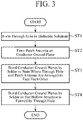
- FIG. 3 is a flowchart illustrating the antenna manufacturing method according to the first embodiment, and illustrates a method for manufacturing the antenna device illustrated in FIG. 1 .
- the through hole 5a is formed in the dielectric substrate 5 (step ST1).
- the through hole 5a is formed to penetrate the dielectric substrate 5 from the conductor ground plane 4 to the conductor ground plane 6.
- the through hole 5a can be formed by, for example, machining by a drill, a punch press machine, or a laser.
- the patch antenna 11 is formed on the conductor ground plane 2 of the dielectric substrate 1 (step ST2).
- the patch antenna 11 is formed on the conductor ground plane 2 at a position to be faced by the through hole 5a when the dielectric substrate 1 is bonded to the dielectric substrate 5.
- the patch antenna 11 to be formed is set on the conductor ground plane 2, and the conductor removed portion 2a is formed by removing the conductor from the conductor ground plane 2 along the outer shape of the patch antenna 11.
- the conductor is removed from the conductor ground plane 2 by copper foil punching such as etching.
- the conductor ground plane 2 of the dielectric substrate 1 and the conductor ground plane 4 of the dielectric substrate 5 are bonded by the solder 3 in a state where the through hole 5a and the patch antenna 11 are arranged to face each other (step ST3).
- the solder 3 is applied to a portion other than the region 3a in the conductor ground plane 2 or the conductor ground plane 4.
- a structure in which the solder 3 is applied between the conductor ground plane 2 and the conductor ground plane 4 is passed through a reflow furnace so that the solder 3 is melted.
- the conductor ground plane 2 and the conductor ground plane 4 are bonded to each other.
- the conductor ground plane 6 of the dielectric substrate 5 and the conductor ground plane 8 of the dielectric substrate 9 are bonded by the solder 7 so that the hollow structure 10 is formed between the dielectric substrate 1 and the dielectric substrate 9 by the through hole 5a (step ST4).
- the solder 7 is applied to a portion other than the region 7a in the conductor ground plane 6 or the conductor ground plane 8.
- a structure in which the solder 7 is applied between the conductor ground plane 6 and the conductor ground plane 8 is passed through a reflow furnace so that the solder 7 is melted.
- the conductor ground plane 6 and the conductor ground plane 8 are bonded to each other.
- steps ST3 and ST4 may be reversed, or these processes may be performed simultaneously.
- a structure in which the solder 3 is applied between the conductor ground plane 2 and the conductor ground plane 4 and the solder 7 is applied between the conductor ground plane 6 and the conductor ground plane 8 may be passed through a reflow furnace so that the solder 3 and the solder 7 are melted, whereby the conductor ground plane 2 and the conductor ground plane 4, and the conductor ground plane 6 and the conductor ground plane 8 may be simultaneously bonded.
- a substrate with an equivalently low dielectric constant can be achieved by providing the hollow structure 10 between the patch antenna 11 and the conductor ground plane 8. Accordingly, the antenna device according to the first embodiment has improved radiation efficiency and improved gain when beam scanning is performed in the wide angle direction, as compared with a typical patch antenna that does not have a hollow structure.
- the gain difference between the vertically polarized wave and the horizontally polarized wave in the wide angle direction in the antenna device according to the first embodiment can be improved by appropriately designing the size of the hollow structure 10.
- the size of the hollow structure 10 may be designed so that the gain difference between the vertically polarized wave and the horizontally polarized wave in the wide angle direction decreases.
- the conductor ground plane 2 may be provided on both the front side and the back side of the dielectric substrate 1.
- the patch antenna 11 may be provided only on the conductor ground plane 2 on the back side of the dielectric substrate 1, or may be provided only on the conductor ground plane 2 on the front side of the dielectric substrate 1.
- the conductor ground plane 2 provided on the dielectric substrate 1 and provided with the patch antenna 11 and the conductor ground plane 4 provided on the side of the dielectric substrate 5 having the through hole 5a are bonded by the solder 3 in a state where the through hole 5a and the patch antenna 11 are arranged to face each other, and the conductor ground plane 6 provided on the back side of the dielectric substrate 5 and the conductor ground plane 8 provided on the dielectric substrate 9 are bonded by the solder 7. Therefore, in the antenna manufacturing method according to the first embodiment, a stress generated inside the dielectric substrate can be minimized as compared with bonding by hot pressing, so that deformation of the antenna can be prevented.
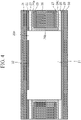
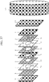
- FIG. 4 is a longitudinal sectional view illustrating a configuration of an antenna device according to the second embodiment.
- FIG. 5 is an exploded perspective view illustrating the configuration of the antenna device shown in FIG. 4 .
- the antenna device according to the second embodiment includes a dielectric substrate 21, a conductor ground plane 22, solder 23, a conductor ground plane 25, a dielectric substrate 26, a conductor ground plane 27, solder 28, a conductor ground plane 29, and a dielectric substrate 30.
- a hollow structure 31 for adjusting an equivalent dielectric constant of the dielectric substrate is provided, and a patch antenna 32 faces the hollow structure 31.
- the dielectric substrate 21 is a first dielectric substrate having the conductor ground plane 22.
- the conductor ground plane 22 is a first conductor ground plane provided on the entire back side of the dielectric substrate 21, and is provided with the patch antenna 32.
- the patch antenna 32 is a first patch antenna formed in a circular shape, and is formed on the conductor ground plane 22 by providing a conductor removed portion 22a in the conductor ground plane 22 as illustrated in FIG. 5 .
- the conductor removed portion 22a is a portion formed by removing the conductor from the conductor ground plane 22 along the outer shape of the patch antenna 32.
- the conductor removed portion 22a is an annular portion formed by removing the conductor from the conductor ground plane 22 as illustrated in FIG. 5 .
- the patch antenna 32 is not limited to one having a circular shape, and it may have, for example, a polygonal shape such as a triangular shape or a quadrangular shape.
- the dielectric substrate 26 is a second dielectric substrate including the conductor ground plane 25 and the conductor ground plane 27.
- the conductor ground plane 25 is a second conductor ground plane provided on the entire front side (first side) of the dielectric substrate 26, and the conductor ground plane 27 is a third conductor ground plane provided on the entire side (back side, second side) opposite to the front side of the dielectric substrate 26.
- the dielectric substrate 26 has a through hole 26a penetrating from the conductor ground plane 25 to the conductor ground plane 27.
- the dielectric substrate 26 in which the through hole 26a is formed is subjected to conductor plating processing.
- conductor plating 24a is provided on an upper layer of the conductor ground plane 25
- conductor plating 26b is provided on the side wall of the through hole 26a
- conductor plating 24c is provided on an upper layer of the conductor ground plane 27 as illustrated in FIGS. 4 and 5 .
- the conductor ground plane 22 of the dielectric substrate 21 and the conductor ground plane 25 of the dielectric substrate 26 are bonded by the solder 23 via the conductor plating 24a in a state where the through hole 26a and the patch antenna 32 are arranged to face each other.
- the dielectric substrate 21 and the dielectric substrate 26 are bonded with the patch antenna 32 facing the through hole 26a as illustrated in FIG. 5 .
- the solder 23 is a first solder for bonding the conductor ground planes.
- the through hole 26a penetrates the dielectric substrate 26 from the conductor ground plane 25 to the conductor ground plane 27. Therefore, as illustrated in FIG. 5 , an opening 24b having the same opening shape as the through hole 26a is formed in the conductor plating 24a, and an opening 25a having the same opening shape as the through hole 26a is formed in the conductor ground plane 25.
- the solder 23 is not applied to a region 23a facing the patch antenna 32 and the conductor removed portion 22a, but applied to a portion other than the region 23a.
- the dielectric substrate 30 is a third dielectric substrate having the conductor ground plane 29.
- the conductor ground plane 29 is a fourth conductor ground plane provided on the entire side of the dielectric substrate 30.
- the conductor ground plane 27 of the dielectric substrate 26 and the conductor ground plane 29 of the dielectric substrate 30 are bonded by the solder 28 via the conductor plating 24c.
- the through hole 26a penetrates the dielectric substrate 26 from the conductor ground plane 25 to the conductor ground plane 27. Therefore, as illustrated in FIG. 5 , an opening 27a having the same opening shape as the through hole 26a is formed in the conductor ground plane 27, and an opening 24d having the same opening shape as the through hole 26a is formed in the conductor plating 24c.
- the solder 28 is a second solder for bonding the conductor ground planes.
- the solder 28 is not applied to a region 28a facing the through hole 26a and the opening 27a, but applied to a portion other than the region 28a in the conductor ground plane 27 or the conductor ground plane 29.
- the hollow structure 31 is constituted by the patch antenna 32, the conductor removed portion 22a, the region 23a, the opening 24b, the opening 25a, the through hole 26a, the opening 27a, the opening 24d, the region 28a, and the conductor ground plane 29.
- the size of the hollow structure 31 is set so that a gain difference between a vertically polarized wave and a horizontally polarized wave decreases when the antenna device illustrated in FIG. 4 performs beam scanning in a wide angle direction. This suppresses a decrease in an axial ratio when beam scanning is performed in the wide angle direction. Note that the solder 23 and the solder 28 are applied in an amount that does not cause leakage into the hollow structure 31 when melted.
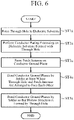
- FIG. 6 is a flowchart illustrating the antenna manufacturing method according to the second embodiment, and illustrates a method for manufacturing the antenna device illustrated in FIG. 4 .
- the through hole 26a is formed in the dielectric substrate 26 (step ST1a).
- the through hole 26a is formed to penetrate the dielectric substrate 26 from the conductor ground plane 25 to the conductor ground plane 27.
- the through hole 26a can be formed by, for example, machining by a drill, a punch press machine, or a laser.
- the dielectric substrate 26 in which the through hole 26a is formed is subjected to conductor plating processing (step ST2a).
- the conductor plating processing a sputtering method or electrolytic plating can be used, for example.
- the conductor plating 24a is provided on the conductor ground plane 25
- the conductor plating 26b is provided on the side wall of the through hole 26a
- the conductor plating 24c is provided on the conductor ground plane 27.
- the patch antenna 32 is formed on the conductor ground plane 22 of the dielectric substrate 21 (step ST3a).
- the patch antenna 32 is formed on the conductor ground plane 22 at a position to be faced by the through hole 26a when the dielectric substrate 21 is bonded to the dielectric substrate 26.
- the patch antenna 32 to be formed is set on the conductor ground plane 22, and the conductor removed portion 22a is formed by removing the conductor from the conductor ground plane 22 along the outer shape of the patch antenna 32.
- the conductor is removed from the conductor ground plane 22 by copper foil punching such as etching.
- the conductor ground plane 22 of the dielectric substrate 21 and the conductor ground plane 25 of the dielectric substrate 26 are bonded by the solder 23 via the conductor plating 24a in a state where the through hole 26a and the patch antenna 32 are arranged to face each other (step ST4a).
- the solder 23 is applied to a portion other than the region 23a in the conductor ground plane 22.
- a structure in which the solder 23 is applied between the conductor ground plane 22 and the conductor ground plane 25 is passed through a reflow furnace so that the solder 23 is melted.
- the conductor ground plane 22 and the conductor ground plane 25 are bonded to each other.
- the conductor ground plane 27 of the dielectric substrate 26 and the conductor ground plane 29 of the dielectric substrate 30 are bonded by the solder 28 via the conductor plating 24c so that the hollow structure 31 is formed between the dielectric substrate 21 and the dielectric substrate 30 by the through hole 26a (step ST5a).
- the solder 28 is applied to a portion other than the region 28a in the conductor ground plane 27.
- a structure in which the solder 28 is applied between the conductor ground plane 27 and the conductor ground plane 29 is passed through a reflow furnace so that the solder 28 is melted.
- the conductor ground plane 27 and the conductor ground plane 29 are bonded to each other.
- steps ST4a and ST5a may be reversed, or these processes may be performed simultaneously.
- a structure in which the solder 23 is applied between the conductor ground plane 22 and the conductor ground plane 25 and the solder 28 is applied between the conductor ground plane 27 and the conductor ground plane 29 may be passed through a reflow furnace so that the solder 23 and the solder 28 are melted, whereby the conductor ground plane 22 and the conductor ground plane 25, and the conductor ground plane 27 and the conductor ground plane 29 may be simultaneously bonded.
- a substrate with an equivalently low dielectric constant can be achieved by providing the hollow structure 31 between the patch antenna 32 and the conductor ground plane 29.
- the conductor plating 26b is provided on the side wall of the hollow structure 31, it is possible to suppress a side wave inside the substrate that causes a decrease in gain when beam scanning is performed in the wide angle direction.
- the gain difference between a vertically polarized wave and a horizontally polarized wave in the wide angle direction in the antenna device according to the second embodiment can be improved by appropriately designing the size of the hollow structure 31.
- the size of the hollow structure 31 may be designed so that the gain difference between the vertically polarized wave and the horizontally polarized wave in the wide angle direction decreases.
- the conductor ground plane 22 may be provided on both the front side and the back side of the dielectric substrate 21.
- the patch antenna 32 may be provided only on the conductor ground plane 22 on the back side of the dielectric substrate 21, or may be provided only on the conductor ground plane 22 on the front side of the dielectric substrate 21.
- the conductor plating processing is performed on the side wall of the through hole 26a. Due to the conductor plating 26b provided on the side wall of the hollow structure 31, it is possible to suppress a surface wave inside the substrate that causes a decrease in gain when beam scanning is performed in the wide angle direction. Furthermore, the antenna device according to the second embodiment has improved radiation efficiency and improved gain when beam scanning is performed in the wide angle direction, as compared with a typical patch antenna that does not have a hollow structure.
- FIG. 7 is a longitudinal sectional view illustrating a configuration of an antenna device according to the third embodiment.
- FIG. 8 is an exploded perspective view illustrating the configuration of the antenna device shown in FIG. 7 .
- the antenna device according to the third embodiment includes a dielectric substrate 41, a conductor ground plane 42, solder 43, a conductor plate 44, solder 45, a conductor ground plane 46, and a dielectric substrate 47.
- a dielectric substrate 47 obtained by bonding the dielectric substrate 41, the conductor plate 44, and the dielectric substrate 47, a hollow structure 48 for adjusting an equivalent dielectric constant of the dielectric substrate is provided, and a patch antenna 49 faces the hollow structure 48.
- the dielectric substrate 41 is a first dielectric substrate having the conductor ground plane 42.
- the conductor ground plane 42 is a first conductor ground plane provided on the entire back side of the dielectric substrate 41, and is provided with the patch antenna 49.
- the patch antenna 49 is a first patch antenna formed in a circular shape, and is formed in the conductor ground plane 42 by providing a conductor removed portion 42a in the conductor ground plane 42 as illustrated in FIG. 8 .
- the conductor removed portion 42a is a portion formed by removing the conductor from the conductor ground plane 42 along the outer shape of the patch antenna 49.
- the conductor removed portion 42a is an annular portion formed by removing the conductor from the conductor ground plane 42 as illustrated in FIG. 8 .
- the patch antenna 49 is not limited to one having a circular shape, and it may have, for example, a polygonal shape such as a triangular shape or a quadrangular shape.
- the conductor plate 44 is a first conductor plate having a through hole 44a.
- the conductor ground plane 42 of the dielectric substrate 41 and the conductor plate 44 are bonded by the solder 43 in a state where the through hole 44a and the patch antenna 49 are arranged to face each other.
- the dielectric substrate 41 and the conductor plate 44 are bonded with the patch antenna 49 facing the through hole 44a as illustrated in FIG. 8 .
- the solder 43 is a first solder for bonding the conductor ground plane and the conductor plate.
- the solder 43 is not applied to a region 43a facing the patch antenna 49 and the conductor removed portion 42a, but applied to a portion other than the region 43a in the conductor ground plane 42 or the conductor plate 44.
- the dielectric substrate 47 is a second dielectric substrate having the conductor ground plane 46.
- the conductor ground plane 46 is a second conductor ground plane provided on the entire side of the dielectric substrate 47.
- the conductor ground plane 46 of the dielectric substrate 47 and the conductor plate 44 are bonded by the solder 45.
- the solder 45 is a second solder for bonding the conductor plate and the conductor ground plane. The solder 45 is not applied to a region 45a facing the through hole 44a, but applied to a portion other than the region 45a in the conductor plate 44 or the conductor ground plane 46.
- the hollow structure 48 is constituted by the patch antenna 49, the conductor removed portion 42a, the region 43a, the through hole 44a, the region 45a, and the conductor ground plane 46.
- the size of the hollow structure 48 is set so that a gain difference between a vertically polarized wave and a horizontally polarized wave decreases when the antenna device illustrated in FIG. 7 performs beam scanning in the wide angle direction. This suppresses a decrease in an axial ratio when beam scanning is performed in the wide angle direction.
- the solder 43 and the solder 45 are applied in an amount that does not cause leakage into the hollow structure 48 when melted.
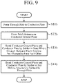
- FIG. 9 is a flowchart illustrating the antenna manufacturing method according to the third embodiment, and illustrates a method for manufacturing the antenna device illustrated in FIG. 7 .
- the through hole 44a is formed in the conductor plate 44 (step ST1b).
- the through hole 44a can be formed by, for example, machining by a drill, a punch press machine, or a laser.
- the patch antenna 49 is formed on the conductor ground plane 42 of the dielectric substrate 41 (step ST2b).
- the patch antenna 49 is formed on the conductor ground plane 42 at a position to be faced by the through hole 44a when the dielectric substrate 41 is bonded to the conductor plate 44.
- the patch antenna 49 to be formed is set on the conductor ground plane 42, and the conductor removed portion 42a is formed by removing the conductor from the conductor ground plane 42 along the outer shape of the patch antenna 49.
- the conductor is removed from the conductor ground plane 42 by copper foil punching such as etching.
- the conductor ground plane 42 of the dielectric substrate 41 and the conductor plate 44 are bonded by the solder 43 in a state where the through hole 44a and the patch antenna 49 are arranged to face each other (step ST3b).
- the solder 43 is applied to a portion other than the region 43a in the conductor ground plane 42.
- a structure in which the solder 43 is applied between the conductor ground plane 42 and the conductor plate 44 is passed through a reflow furnace so that the solder 43 is melted.
- the conductor ground plane 42 and the conductor plate 44 are bonded to each other.
- the conductor plate 44 and the conductor ground plane 46 of the dielectric substrate 47 are bonded by the solder 45 so that the hollow structure 48 is formed between the dielectric substrate 41 and the dielectric substrate 47 by the through hole 44a (step ST4b).
- the solder 45 is applied to a portion other than the region 45a in the conductor plate 44 or the conductor ground plane 46.
- a structure in which the solder 45 is applied between the conductor plate 44 and the conductor ground plane 46 is passed through a reflow furnace so that the solder 45 is melted.
- the conductor plate 44 and the conductor ground plane 46 are bonded to each other.
- steps ST3b and ST4b may be reversed, or these processes may be performed simultaneously.
- a structure in which the solder 43 is applied between the conductor ground plane 42 and the conductor plate 44 and the solder 45 is applied between the conductor plate 44 and the conductor ground plane 46 may be passed through a reflow furnace so that the solder 43 and the solder 45 are melted, whereby the conductor ground plane 42 and the conductor plate 44, and the conductor plate 44 and the conductor ground plane 46 may be simultaneously bonded.
- a substrate with an equivalently low dielectric constant can be achieved by providing the hollow structure 48 between the patch antenna 49 and the conductor ground plane 46.
- the antenna device according to the third embodiment has improved radiation efficiency and improved gain when beam scanning is performed in the wide angle direction, as compared with a typical patch antenna that does not have a hollow structure.
- the gain difference between the vertically polarized wave and the horizontally polarized wave in the wide angle direction in the antenna device according to the third embodiment can be improved by appropriately designing the size of the hollow structure 48.
- the size of the hollow structure 48 may be designed so that the gain difference between the vertically polarized wave and the horizontally polarized wave in the wide angle direction decreases.
- the conductor ground plane 42 may be provided on both the front side and the back side of the dielectric substrate 41.
- the patch antenna 49 may be provided only on the conductor ground plane 42 on the back side of the dielectric substrate 41, or may be provided only on the conductor ground plane 42 on the front side of the dielectric substrate 41.
- the conductor ground plane 42 of the dielectric substrate 41 and the conductor plate 44 are bonded by the solder 43 in a state where the through hole 44a and the patch antenna 49 are arranged to face each other, and the conductor plate 44 and the conductor ground plane 46 of the dielectric substrate 47 are bonded by the solder 45.
- the same effects as those of the first embodiment can be obtained.
- the side wall of the hollow structure 48 being a conductor side, it is possible to suppress a surface wave inside the substrate that causes a decrease in gain when beam scanning is performed in the wide angle direction. This improves the radiation efficiency, and improves a gain when beam scanning is performed in the wide angle direction, as compared to a typical patch antenna that does not have a hollow structure.
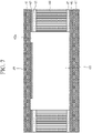
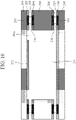
- FIG. 10 is a longitudinal sectional view illustrating a configuration of an antenna device according to the fourth embodiment.
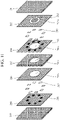
- FIG. 11 is an exploded perspective view illustrating the configuration of the antenna device shown in FIG. 10 .
- the antenna device according to the fourth embodiment includes a dielectric substrate 201, a conductor ground plane 202, solder 203, a conductor ground plane 204, a dielectric substrate 205, a conductor ground plane 206, solder 207, a conductor ground plane 208, and a dielectric substrate 209.
- a hollow structure 211 for adjusting an equivalent dielectric constant of the dielectric substrate is provided, and a patch antenna 212 faces the hollow structure 211.
- the dielectric substrate 201 is a first dielectric substrate having the conductor ground plane 202.
- the conductor ground plane 202 is a first conductor ground plane provided on the entire back side of the dielectric substrate 201, and is provided with the patch antenna 212.
- the patch antenna 212 is a first patch antenna formed in a circular shape. As illustrated in FIG. 11 , the patch antenna 212 is formed on the conductor ground plane 202 by providing a conductor removed portion 202a in the conductor ground plane 202.
- the conductor removed portion 202a is a portion formed by removing the conductor from the conductor ground plane 202 along the outer shape of the patch antenna 212.
- the conductor removed portion 202a is an annular portion formed by removing the conductor from the conductor ground plane 202 as illustrated in FIG. 11 .
- the patch antenna 212 is not limited to one having a circular shape, and it may have, for example, a polygonal shape such as a triangular shape or a quadrangular shape.
- the dielectric substrate 205 is a second dielectric substrate including the conductor ground plane 204 and the conductor ground plane 206.
- the conductor ground plane 204 is a second conductor ground plane provided on the entire front side (first side) of the dielectric substrate 205
- the conductor ground plane 206 is a third conductor ground plane provided on the entire side (back side, second side) opposite to the front side of the dielectric substrate 205.
- the dielectric substrate 205 has a through hole 205a penetrating from the conductor ground plane 204 to the conductor ground plane 206.
- the conductor ground plane 202 of the dielectric substrate 201 and the conductor ground plane 204 of the dielectric substrate 205 are bonded by the solder 203 in a state where the through hole 205a and the patch antenna 212 are arranged to face each other.
- the dielectric substrate 201 and the dielectric substrate 205 are bonded with the patch antenna 212 facing the through hole 205a as illustrated in FIG. 11 .
- the solder 203 is a first solder for bonding the conductor ground planes.
- the through hole 205a penetrates the dielectric substrate 205 from the conductor ground plane 204 to the conductor ground plane 206. Therefore, as illustrated in FIG. 11 , an opening 204a having the same opening shape as the through hole 205a is formed in the conductor ground plane 204, and an opening 206a having the same opening shape as the through hole 205a is formed in the conductor ground plane 206.
- the dielectric substrate 209 is a third dielectric substrate having the conductor ground plane 208.
- the conductor ground plane 208 is a fourth conductor ground plane provided on the entire side of the dielectric substrate 209.
- the conductor ground plane 206 of the dielectric substrate 205 and the conductor ground plane 208 of the dielectric substrate 209 are bonded by the solder 207.
- bonding using the solder 203 and the solder 207 is performed on lands 210.
- the lands 210 are small regions for bonding using solder formed at a bonding portion between the conductor ground plane 202 and the conductor ground plane 204. Since the bonding using the solder 203 and the solder 207 is performed on the lands 210, the bonding positions using the solder can be accurately disposed.
- the positions of the lands 210 in the conductor ground plane 202 and in the conductor ground plane 204 face each other.
- the lands 210 can be disposed at any position in a region other than the opening 204a in the conductor ground plane 204, and an amount of the solder 203 applied to the lands 210 is also freely set.
- the positions of the lands 210 in the conductor ground plane 206 and in the conductor ground plane 208 face each other.
- the lands 210 can be disposed at any position in a region other than the opening 206a in the conductor ground plane 206, and an amount of the solder 207 applied to the lands 210 is also freely set.
- the hollow structure 211 is constituted by the patch antenna 212, the conductor removed portion 202a, the opening 204a, the through hole 205a, the opening 206a, and the conductor ground plane 208.
- the size of the hollow structure 211 is set so that a gain difference between a vertically polarized wave and a horizontally polarized wave decreases when the antenna device illustrated in FIG. 10 performs beam scanning in a wide angle direction. This suppresses a decrease in an axial ratio when beam scanning is performed in the wide angle direction.
- the antenna manufacturing method according to the fourth embodiment is basically the same as the series of processing illustrated in FIG. 3 except that the bonding using solder in steps ST3 and ST4 is performed on the lands 210.
- step ST3 the conductor ground plane 202 of the dielectric substrate 201 and the conductor ground plane 204 of the dielectric substrate 205 are bonded by the solder 203 on the lands 210 in a state where the through hole 205a and the patch antenna 212 are arranged to face each other.
- a structure including the conductor ground plane 202 and the conductor ground plane 204 bonded by the solder 203 applied to the lands 210 is passed through a reflow furnace to melt the solder 203, whereby the conductor ground plane 202 and the conductor ground plane 204 are bonded.
- step ST4 the conductor ground plane 206 of the dielectric substrate 205 and the conductor ground plane 208 of the dielectric substrate 209 are bonded by the solder 207 on the lands 210 so that the hollow structure 211 is formed between the dielectric substrate 201 and the dielectric substrate 209 by the through hole 205a.
- a structure including the conductor ground plane 206 and the conductor ground plane 208 bonded by the solder 207 applied to the lands 210 is passed through a reflow furnace to melt the solder 207, whereby the conductor ground plane 206 and the conductor ground plane 208 are bonded.
- steps ST3 and ST4 described above may be reversed, or these processes may be performed simultaneously.
- a structure in which the solder 203 is applied to the lands 210 between the conductor ground plane 202 and the conductor ground plane 204 and the solder 207 is applied to the lands 210 between the conductor ground plane 206 and the conductor ground plane 208 may be passed through a reflow furnace so that the solder 203 and the solder 207 are melted, whereby the conductor ground plane 202 and the conductor ground plane 204, and the conductor ground plane 206 and the conductor ground plane 208 may be simultaneously bonded.
- the conductor ground plane 202 may be provided on both the front side and the back side of the dielectric substrate 201.
- the patch antenna 212 may be provided only on the conductor ground plane 202 on the back side of the dielectric substrate 201, or may be provided only on the conductor ground plane 202 on the front side of the dielectric substrate 201.
- the bonding using the solder 203 and the solder 207 is performed on the lands 210.
- bonding positions using the solder can be accurately determined.
- the antenna device according to the fourth embodiment has improved radiation efficiency and improved gain when beam scanning is performed in the wide angle direction, as compared with a typical patch antenna that does not have a hollow structure.
- FIG. 12 is a longitudinal sectional view illustrating a configuration of an antenna device according to the fifth embodiment.
- FIG. 13 is an exploded perspective view illustrating the configuration of the antenna device shown in FIG. 12 .
- the antenna device according to the fifth embodiment includes a dielectric substrate 101, a conductor ground plane 102, a prepreg 103, a dielectric substrate 104, a prepreg 105, a conductor ground plane 106, and a dielectric substrate 107.
- a hollow structure 108 for adjusting an equivalent dielectric constant of the dielectric substrate is provided, and a patch antenna 109 faces the hollow structure 108.
- the dielectric substrate 101 is a first dielectric substrate having the conductor ground plane 102.
- the conductor ground plane 102 is a first conductor ground plane provided on the entire back side of the dielectric substrate 101, and is provided with the patch antenna 109.
- the patch antenna 109 is a first patch antenna formed in a circular shape, and is formed on the conductor ground plane 102 by providing a conductor removed portion 102a in the conductor ground plane 102 as illustrated in FIG. 13 .
- the conductor removed portion 102a is a portion formed by removing the conductor from the conductor ground plane 102 along the outer shape of the patch antenna 109.
- the conductor removed portion 102a is an annular portion formed by removing the conductor from the conductor ground plane 102 as illustrated in FIG. 13 .
- the patch antenna 109 is not limited to one having a circular shape, and it may have, for example, a polygonal shape such as a triangular shape or a quadrangular shape.
- the dielectric substrate 104 is a second dielectric substrate provided with a plurality of through holes 104a having an opening area smaller than the area of the patch antenna 109.
- the dielectric substrate 107 is a third dielectric substrate having the conductor ground plane 106 formed on the side.
- the conductor ground plane 106 is a second conductor ground plane provided on the entire side of the dielectric substrate 107. It is possible to reduce the equivalent dielectric constant from the patch antenna 109 to the conductor ground plane 106 by increasing the number of the through holes 104a.
- the prepreg 103 and the prepreg 105 are dielectric adhesives.
- the prepreg 103 is provided between the conductor ground plane 102 and the front side of the dielectric substrate 104
- the prepreg 105 is provided between the back side of the dielectric substrate 104 and the conductor ground plane 106.
- the prepreg 103 has an opening 103a formed by removing a portion corresponding to a region of the dielectric substrate 104 where the plurality of through holes 104a is formed.
- the prepreg 105 has an opening 105a formed by removing a portion corresponding to the region of the dielectric substrate 104 where the plurality of through holes 104a is formed.
- the prepreg 103 bonds the conductor ground plane 102 and the side of dielectric substrate 104 by hot pressing, and the prepreg 105 bonds the back side of the dielectric substrate 104 and the conductor ground plane 106 by hot pressing.
- the dielectric substrates are bonded by hot pressing. Therefore, a thermoplastic resin film or a thermosetting resin film may be used instead of the prepreg 103 and the prepreg 105.
- the hollow structure 108 is constituted by the patch antenna 109, the conductor removed portion 102a, the opening 103a, the plurality of through holes 104a, the opening 105a, and the conductor ground plane 106. Since the opening area of each of the plurality of through holes 104a is smaller than the area of the patch antenna 109, the deformation of the dielectric substrate 101 and the dielectric substrate 107 toward the hollow structure 108 is restricted by the portion other than the through holes 104a in the dielectric substrate 104. Thus, even if stress is generated inside the dielectric substrates by hot pressing, deformation of the dielectric substrates toward the hollow structure 108 is suppressed.
- the number of the through holes 104a is set so that a gain difference between a vertically polarized wave and a horizontally polarized wave decreases when the antenna device illustrated in FIG. 12 performs beam scanning in the wide angle direction. This suppresses a decrease in an axial ratio when beam scanning is performed in the wide angle direction.
- FIG. 14 is a flowchart illustrating the antenna manufacturing method according to the fifth embodiment, and illustrates a method for manufacturing the antenna device illustrated in FIG. 12 .
- a plurality of through holes 104a is formed in the dielectric substrate 104 (step ST1c).
- the through holes 104a are formed by, for example, machining by a drill, a punch press machine, or a laser.
- the patch antenna 109 is formed on the conductor ground plane 102 of the dielectric substrate 101 (step ST2c).
- the patch antenna 109 is formed on the conductor ground plane 102 at a position to be faced by the through holes 104a when the dielectric substrate 101 is bonded to the dielectric substrate 104.
- the patch antenna 109 to be formed is set on the conductor ground plane 102, and the conductor removed portion 102a is formed by removing the conductor from the conductor ground plane 102 along the outer shape of the patch antenna 109.
- the conductor is removed from the conductor ground plane 102 by copper foil punching such as etching.
- the prepreg 103 is disposed between the conductor ground plane 102 of the dielectric substrate 101 and the front side of the dielectric substrate 104, and the prepreg 105 is disposed between the back side of the dielectric substrate 104 and the conductor ground plane 106 of the dielectric substrate 107.
- the dielectric substrates are bonded by hot pressing (step ST3c).
- the prepreg 103 softened by heating is pressed to bond the conductor ground plane 102 and the front side of the dielectric substrate 104, and the prepreg 105 softened by heating is pressed to bond the back side of the dielectric substrate 104 and the conductor ground plane 106.
- a substrate with an equivalently low dielectric constant can be achieved by providing the hollow structure 108 between the patch antenna 109 and the conductor ground plane 106.
- the antenna device according to the fifth embodiment has improved radiation efficiency and improved gain when beam scanning is performed in the wide angle direction, as compared with a typical patch antenna that does not have a hollow structure.
- the gain difference between the vertically polarized wave and the horizontally polarized wave in the wide angle direction in the antenna device according to the fifth embodiment can be improved by appropriately designing the size of the hollow structure 108.
- the size of the hollow structure 108 may be designed so that the gain difference between the vertically polarized wave and the horizontally polarized wave in the wide angle direction decreases.
- the conductor ground plane 102 may be provided on both the front side and the back side of the dielectric substrate 101.
- the patch antenna 109 may be provided only on the conductor ground plane 102 on the back side of the dielectric substrate 101, or may be provided only on the conductor ground plane 102 on the front side of the dielectric substrate 101.
- the dielectric substrate 101, the dielectric substrate 104, and the dielectric substrate 107 are bonded by hot pressing in a state where the positions of the plurality of through holes 104a and the patch antenna 109 face each other. Since the opening area of each of the plurality of through holes 104a is smaller than the area of the patch antenna 109, the deformation of the dielectric substrate 101 and the dielectric substrate 107 toward the hollow structure 108 is restricted by the portion other than the through holes 104a in the dielectric substrate 104. Furthermore, the equivalent dielectric constant from the patch antenna 109 to the conductor ground plane 106 can be reduced by increasing the number of through holes 104a. Therefore, compared with a typical patch antenna without the hollow structure 108, the radiation efficiency is improved, and the gain when beam scanning is performed in the wide angle direction is improved.
- FIG. 15 is a longitudinal sectional view illustrating a configuration of an antenna device according to the sixth embodiment.
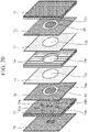
- FIG. 16 is an exploded perspective view illustrating the configuration of the antenna device shown in FIG. 15 .
- the antenna device according to the sixth embodiment includes a dielectric substrate 221, a conductor ground plane 222, a prepreg 223, a dielectric substrate 224, a prepreg 225, a conductor ground plane 226, and a dielectric substrate 227.
- a hollow structure 228 for adjusting an equivalent dielectric constant of the dielectric substrate is provided, and a patch antenna 229 faces the hollow structure 228.
- the dielectric substrate 221 is a first dielectric substrate having the conductor ground plane 222.
- the conductor ground plane 222 is a first conductor ground plane provided on the entire back side of the dielectric substrate 221, and is provided with a patch antenna 229.
- the patch antenna 229 is a first patch antenna formed in a circular shape, and is formed on the conductor ground plane 222 by providing a conductor removed portion 222a in the conductor ground plane 222 as illustrated in FIG. 16 .
- the conductor removed portion 222a is a portion formed by removing the conductor from the conductor ground plane 222 along the outer shape of the patch antenna 229.
- the conductor removed portion 222a is an annular portion formed by removing the conductor from the conductor ground plane 222 as illustrated in FIG. 16 .
- the patch antenna 229 is not limited to one having a circular shape, and it may have, for example, a polygonal shape such as a triangular shape or a quadrangular shape.
- the dielectric substrate 224 is a second dielectric substrate provided with a through hole 224a having an opening area smaller than the area of the patch antenna 229.
- the dielectric substrate 227 is a third dielectric substrate having the conductor ground plane 226 formed on the side.
- the conductor ground plane 226 is a second conductor ground plane provided on the entire side of the dielectric substrate 227.
- the through hole 224a is a hole having a groove shape along the outer shape of the patch antenna 229 when the patch antenna 229 is projected from the conductor ground plane 222 onto the dielectric substrate 224.
- a portion inside the through hole 224a is bonded to the dielectric substrate 224 by a support portion 224b. It is possible to reduce the equivalent dielectric constant from the patch antenna 229 to the conductor ground plane 226 by appropriately designing the size of the through hole 224a.
- the prepreg 223 and the prepreg 225 are dielectric adhesives.
- the prepreg 223 is provided between the conductor ground plane 222 and the front side of the dielectric substrate 224, and the prepreg 225 is provided between the back side of the dielectric substrate 224 and the conductor ground plane 226.
- the prepreg 223 has an opening 223a formed by removing a portion corresponding to the patch antenna 229 and the conductor removed portion 222a.
- the prepreg 225 also has an opening 225a formed by removing a portion corresponding to the patch antenna 229 and the conductor removed portion 222a.
- the prepreg 223 bonds the conductor ground plane 222 and the side of the dielectric substrate 224 by hot pressing, and the prepreg 225 bonds the back side of the dielectric substrate 224 and the conductor ground plane 226 by hot pressing.
- the dielectric substrates are bonded by hot pressing. Therefore, a thermoplastic resin film or a thermosetting resin film may be used instead of the prepreg 223 and the prepreg 225.
- the hollow structure 228 is constituted by the patch antenna 229, the conductor removed portion 222a, the opening 223a, the through hole 224a, the opening 225a, and the conductor ground plane 226.
- the opening area of the through hole 224a is smaller than the area of the patch antenna 229.
- the size of the through hole 224a is set so that a gain difference between a vertically polarized wave and a horizontally polarized wave decreases when the antenna device illustrated in FIG. 15 performs beam scanning in the wide angle direction. This suppresses a decrease in an axial ratio when beam scanning is performed in the wide angle direction.
- the antenna manufacturing method according to the sixth embodiment is basically the same as the series of processing described with reference to FIG. 14 except that the plurality of through holes 104a in the fifth embodiment is replaced by the annular through hole 224a. Therefore, the description thereof will be omitted.
- a substrate with an equivalently low dielectric constant can be achieved by providing the hollow structure 228 between the patch antenna 229 and the conductor ground plane 226.
- the antenna device according to the sixth embodiment has improved radiation efficiency and improved gain when beam scanning is performed in the wide angle direction, as compared with a typical patch antenna that does not have a hollow structure.
- the gain difference between the vertically polarized wave and the horizontally polarized wave in the wide angle direction in the antenna device according to the sixth embodiment can be improved by appropriately designing the size of the hollow structure 228.
- the size of the hollow structure 228 may be designed so that the gain difference between the vertically polarized wave and the horizontally polarized wave in the wide angle direction decreases.
- the conductor ground plane 222 may be provided on both the front side and the back side of the dielectric substrate 221.
- the patch antenna 229 may be provided only on the conductor ground plane 222 on the back side of the dielectric substrate 221, or may be provided only on the conductor ground plane 222 on the front side of the dielectric substrate 221.
- the dielectric substrate 221, the dielectric substrate 224, and the dielectric substrate 227 are bonded in a state where the positions of the groove-shaped through hole 224a along the outer shape of the patch antenna 229 projected on the dielectric substrate 224 and the patch antenna 229 face each other. Since the opening area of the through hole 224a is smaller than the area of the patch antenna 229, the deformation of the dielectric substrate 221 and the dielectric substrate 227 toward the hollow structure 108 is restricted by the portion other than the through hole 224a in the dielectric substrate 224. Furthermore, the equivalent dielectric constant from the patch antenna 229 to the conductor ground plane 226 can be reduced depending on the size of the through hole 224a. Therefore, compared with a typical patch antenna without the hollow structure 228, the radiation efficiency is improved, and the gain when beam scanning is performed in the wide angle direction is improved.
- FIG. 17 is a longitudinal sectional view illustrating a configuration of an antenna device according to the seventh embodiment.
- FIG. 18 is an exploded perspective view illustrating the configuration of the antenna device shown in FIG. 17 .
- the antenna device according to the seventh embodiment includes a dielectric substrate 50, a conductor ground plane 51, solder 52, a conductor ground plane 54, a dielectric substrate 55, a conductor ground plane 56, solder 57, a conductor ground plane 58, a dielectric substrate 59, and a conductor ground plane 60.
- a hollow structure 65 for adjusting an equivalent dielectric constant of the dielectric substrate is provided, and a first patch antenna 63 and a second patch antenna 64 face the hollow structure 65.
- the dielectric substrate 50 is a first dielectric substrate having the conductor ground plane 51.
- the conductor ground plane 51 is a first conductor ground plane provided on the entire back side of the dielectric substrate 50, and is provided with the first patch antenna 63.
- the first patch antenna 63 is formed in a circular shape. As illustrated in FIG. 18 , the first patch antenna 63 is formed on the conductor ground plane 51 by providing a conductor removed portion 51a in the conductor ground plane 51.
- the conductor removed portion 51a is a portion formed by removing the conductor from the conductor ground plane 51 along the outer shape of the first patch antenna 63.
- the conductor removed portion 51a is an annular portion obtained by removing the conductor from the conductor ground plane 51 as illustrated in FIG. 18 .
- the first patch antenna 63 is not limited to one having a circular shape, and it may have, for example, a polygonal shape such as a triangular shape or a quadrangular shape.
- the dielectric substrate 55 is a second dielectric substrate including the conductor ground plane 54 and the conductor ground plane 56.
- the conductor ground plane 54 is a second conductor ground plane provided on the entire front side (first side) of the dielectric substrate 55
- the conductor ground plane 56 is a third conductor ground plane provided on the entire side (back side, second side) opposite to the front side of the dielectric substrate 55.
- the dielectric substrate 55 has a through hole 55a penetrating from the conductor ground plane 54 to the conductor ground plane 56.
- the dielectric substrate 55 in which the through hole 55a is formed is subjected to conductor plating processing.
- conductor plating 53a is provided on an upper layer of the conductor ground plane 54
- conductor plating 55b is formed on the side wall of the through hole 55a
- conductor plating 53c is provided on an upper layer of the conductor ground plane 56.
- the conductor ground plane 51 of the dielectric substrate 50 and the conductor ground plane 54 of the dielectric substrate 55 are bonded by the solder 52 via the conductor plating 53a in a state where the through hole 55a and the first patch antenna 63 face each other.
- the dielectric substrate 50 and the dielectric substrate 55 are bonded with the first patch antenna 63 facing the through hole 55a as illustrated in FIG. 17 .
- the solder 52 is a first solder for bonding the conductor ground planes.
- the through hole 55a penetrates the dielectric substrate 55 from the conductor ground plane 54 to the conductor ground plane 56. Therefore, an opening 53b having the same opening shape as the through hole 55a is formed in the conductor plating 53a, an opening 53d having the same opening shape as the through hole 55a is formed in the conductor plating 53c, an opening 54a having the same opening shape as the through hole 55a is formed in the conductor ground plane 54, and an opening 56a having the same opening shape as the through hole 55a is formed in the conductor ground plane 56, as illustrated in FIG. 18 .
- the solder 52 is not applied to a region 52a facing the first patch antenna 63 and the conductor removed portion 51a, but applied to a portion other than the region 52a in the conductor ground plane 51 or the conductor plating 53a.
- the dielectric substrate 59 is a third dielectric substrate including the conductor ground plane 58 and the conductor ground plane 60.
- the conductor ground plane 58 is a fourth conductor ground plane provided on the entire front side (first side) of the dielectric substrate 59, and is provided with the second patch antenna 64.
- the conductor ground plane 60 is a fifth conductor ground plane provided on the entire side (back side, second side) opposite to the front side of the dielectric substrate 59.
- the second patch antenna 64 has a circular shape with a diameter smaller than that of the first patch antenna 63. As illustrated in FIG. 18 , the second patch antenna 64 is formed on the conductor ground plane 58 by providing a conductor removed portion 58a in the conductor ground plane 58.
- the conductor removed portion 58a is a portion formed by removing the conductor from the conductor ground plane 58 along the outer shape of the second patch antenna 64.
- the conductor removed portion 58a is an annular portion formed by removing the conductor from the conductor ground plane 58 as illustrated in FIG. 18 .
- the second patch antenna 64 is not limited to one having a circular shape, and it may have, for example, a polygonal shape such as a triangular shape or a quadrangular shape.
- the conductor ground plane 58 of the dielectric substrate 59 and the conductor ground plane 56 of the dielectric substrate 55 are bonded by the solder 57 via the conductor plating 53c in a state where the through hole 55a and the second patch antenna 64 are arranged to face each other.
- the dielectric substrate 55 and the dielectric substrate 59 are bonded with the second patch antenna 64 facing the through hole 55a as illustrated in FIG. 18 .
- the solder 57 is a second solder for bonding the conductor ground planes. The solder 57 is not applied to a region 57a facing the through hole 55a.
- a via 61a and a via 61b are formed, and a first feeding pin 62a and a second feeding pin 62b are formed.
- the via 61a and the via 61b electrically connect the conductor ground plane 60 and the conductor ground plane 58.
- the conductor ground plane 58 is bonded to the conductor ground plane 56 by the solder 57
- the conductor ground plane 56 is electrically bonded to the conductor ground plane 54 by the conductor plating 55b
- the conductor ground plane 54 is bonded to the conductor ground plane 51 by the solder 52. Therefore, due to the via 61a and the via 61b being provided, the potential from the conductor ground plane 60 to the conductor ground plane 51 is the same.
- the vias 61a and 61b are provided so as to surround the second patch antenna 64.
- the first feeding pin 62a and the second feeding pin 62b have a feeding structure for feeding power to the second patch antenna 64.
- a first polarized wave is fed to the first feeding pin 62a
- a second polarized wave orthogonal to the first polarized wave is fed to the second feeding pin 62b.
- the second patch antenna 64 operates as an antenna by being fed with power from the first feeding pin 62a and the second feeding pin 62b.
- a feeding structure using slot coupling or spatial coupling of microstrip lines may be used as the structure for feeding power to the second patch antenna 64.
- the hollow structure 65 is constituted by the first patch antenna 63, the conductor removed portion 51a, the region 52a, the opening 53b, the opening 54a, the through hole 55a, the opening 56a, the opening 56a, the opening 53d, the region 57a, and the second patch antenna 64.
- the size of the hollow structure 65 is set so that a gain difference between a vertically polarized wave and a horizontally polarized wave decreases when the antenna device illustrated in FIG. 17 performs beam scanning in a wide angle direction. This suppresses a decrease in an axial ratio when beam scanning is performed in the wide angle direction.
- the solder 52 and the solder 57 are applied in an amount that does not cause leakage into the hollow structure 31 when melted.
- the conductor ground plane 51 may be provided on both the front side and the back side of the dielectric substrate 50.
- the first patch antenna 63 may be provided only on the conductor ground plane 51 on the back side of the dielectric substrate 50, or may be provided only on the conductor ground plane 51 on the front side of the dielectric substrate 50.
- the antenna device includes the first feeding pin 62a and the second feeding pin 62b which are provided on the dielectric substrate 59, and the second patch antenna 64 which is provided on the dielectric substrate 59 and fed with power from the first feeding pin 62a and the second feeding pin 62b. Since the hollow structure 65 is provided immediately below the parasitic first patch antenna 63, cross polarization can be suppressed. In addition, circularly polarized waves can be radiated by feeding power having phases different by 90 degrees to the first feeding pin 62a and the second feeding pin 62b.
- FIG. 19 is a longitudinal sectional view illustrating a configuration of an antenna device according to the eighth embodiment.
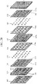
- FIG. 20 is an exploded perspective view illustrating the configuration of the antenna device shown in FIG. 19 .
- the antenna device according to the eighth embodiment includes a dielectric substrate 71, a conductor ground plane 72, solder 73, a conductor plate 74, solder 75, a conductor ground plane 76, a dielectric substrate 77, and a conductor ground plane 78.
- a hollow structure 84 for adjusting an equivalent dielectric constant of the dielectric substrate is provided, and a first patch antenna 80 and a second patch antenna 82 face the hollow structure 84.
- the dielectric substrate 71 is a first dielectric substrate having the conductor ground plane 72.
- the conductor ground plane 72 is a first conductor ground plane provided on the entire back side of the dielectric substrate 71, and is provided with the first patch antenna 80.
- the first patch antenna 80 is formed in a circular shape, and is provided on the conductor ground plane 72 by providing a conductor removed portion 72a in the conductor ground plane 72 as illustrated in FIG. 18 .
- the conductor removed portion 72a is a portion formed by removing the conductor from the conductor ground plane 72 along the outer shape of the first patch antenna 80.
- the conductor removed portion 72a is an annular portion formed by removing the conductor from the conductor ground plane 72 as illustrated in FIG. 20 .
- the first patch antenna 80 is not limited to one having a circular shape, and it may have, for example, a polygonal shape such as a triangular shape or a quadrangular shape.
- the conductor plate 74 is a first conductor plate having a through hole 74a.
- the conductor ground plane 72 of the dielectric substrate 71 and the conductor plate 74 are bonded by the solder 73 in a state where the through hole 74a and the first patch antenna 80 are arranged to face each other.
- the dielectric substrate 71 and the conductor plate 74 are bonded with the first patch antenna 80 facing the through hole 74a as illustrated in FIG. 20 .
- the solder 73 is a first solder for bonding the conductor ground plane and the conductor plate.
- the solder 73 is not applied to a region 73a facing the first patch antenna 80 and the conductor removed portion 72a, but applied to a portion other than the region 73a in the conductor ground plane 72 or the conductor plate 74.
- the dielectric substrate 77 is a second dielectric substrate including the conductor ground plane 76 and the conductor ground plane 78.
- the conductor ground plane 76 is a second conductor ground plane provided on the entire front side of the dielectric substrate 77
- the conductor ground plane 78 is a third conductor ground plane provided on the entire back side of the dielectric substrate 77.
- the conductor ground plane 76 of the dielectric substrate 77 and the conductor plate 74 are bonded by the solder 75.
- the solder 75 is a second solder for bonding the conductor plate and the conductor ground plane. The solder 75 is not applied to a region 75a facing the through hole 74a, but applied to a portion other than the region 75a in the conductor ground plane 76.
- the second patch antenna 82 is a circular patch antenna having a diameter smaller than that of the first patch antenna 80. As illustrated in FIG. 20 , the second patch antenna 82 is formed in the conductor ground plane 76 by providing a conductor removed portion 76a in the conductor ground plane 76.
- the conductor removed portion 76a is a portion formed by removing the conductor from the conductor ground plane 76 along the outer shape of the second patch antenna 82.
- the conductor removed portion 76a is an annular portion formed by removing the conductor from the conductor ground plane 76 as illustrated in FIG. 20 .
- the second patch antenna 82 is not limited to one having a circular shape, and it may have, for example, a polygonal shape such as a triangular shape or a quadrangular shape.
- the conductor ground plane 72 of the dielectric substrate 71 and the conductor plate 74 are bonded by the solder 73 in a state where the through hole 74a and the first patch antenna 80 are arranged to face each other.
- the dielectric substrate 71 and the conductor plate 74 are bonded with the first patch antenna 80 facing the through hole 74a as illustrated in FIG. 20 .
- a via 79a and a via 79b are formed, and a first feeding pin 81a and a second feeding pin 81b are formed.
- the via 79a and the via 79b electrically connect the conductor ground plane 76 and the conductor ground plane 78.
- the conductor ground plane 76 is bonded to the conductor plate 74 by the solder 75, and the conductor plate 74 is bonded to the conductor ground plane 72 by the solder 73. Since the via 79a and the via 79b are provided, the potential from the conductor ground plane 78 to the conductor ground plane 72 is the same.
- the vias 79a and 79b are provided so as to surround the second patch antenna 82.
- the first feeding pin 81a and the second feeding pin 81b have a feeding structure for feeding power to the second patch antenna 82.
- a first polarized wave is fed to the first feeding pin 81a
- a second polarized wave orthogonal to the first polarized wave is fed to the second feeding pin 81b.
- the second patch antenna 82 operates as an antenna by being fed with power from the first feeding pin 81a and the second feeding pin 81b.
- a feeding structure using slot coupling or spatial coupling of microstrip lines may be used as the structure for feeding power to the second patch antenna 82.
- the hollow structure 84 is constituted by the first patch antenna 80, the conductor removed portion 72a, the region 73a, the through hole 74a, the region 75a, and the second patch antenna 82.
- the size of the hollow structure 84 is set so that a gain difference between a vertically polarized wave and a horizontally polarized wave decreases when the antenna device illustrated in FIG. 19 performs beam scanning in a wide angle direction. This suppresses a decrease in an axial ratio when beam scanning is performed in the wide angle direction.
- the solder 73 and the solder 75 are applied in an amount that does not cause leakage into the hollow structure 84 when melted.
- the conductor ground plane 72 may be provided on both the front side and the back side of the dielectric substrate 71.
- the first patch antenna 80 may be provided only on the conductor ground plane 72 on the back side of the dielectric substrate 71, or may be provided only on the conductor ground plane 72 on the front side of the dielectric substrate 71.
- the dielectric substrate 71 may have a via.
- the antenna device includes the first feeding pin 81a and the second feeding pin 81b which are provided on the dielectric substrate 77, and the second patch antenna 82 which is provided on the dielectric substrate 77 and fed with power from the first feeding pin 81a and the second feeding pin 81b. Since the hollow structure 84 is provided immediately below the parasitic first patch antenna 80, cross polarization can be suppressed. In addition, circularly polarized waves can be radiated by feeding power having phases different by 90 degrees to the first feeding pin 81a and the second feeding pin 81b.
- FIG. 21 is a longitudinal sectional view illustrating a configuration of an antenna device according to the ninth embodiment.
- FIG. 22 is an exploded perspective view illustrating the configuration of the antenna device shown in FIG. 21 .
- the antenna device according to the ninth embodiment includes a dielectric substrate 121, a conductor ground plane 122, solder 123, a conductor ground plane 124, a dielectric substrate 125, a conductor ground plane 126, solder 127, a conductor ground plane 128, a dielectric substrate 129, and a conductor ground plane 130.
- a plurality of hollow structures 132 for adjusting an equivalent dielectric constant of the dielectric substrate is provided, and a first patch antenna 133 and a second patch antenna 131 face each of the hollow structures 132.
- the dielectric substrate 121 is a first dielectric substrate having the conductor ground plane 122.
- the conductor ground plane 122 is a first conductor ground plane provided on the entire back side of the dielectric substrate 121, and is provided with a plurality of first patch antennas 133.
- Each of the plurality of first patch antennas 133 is formed in a circular shape, and is formed in the conductor ground plane 122 by providing a conductor removed portion 122a in the conductor ground plane 122 as illustrated in FIG. 22 .
- the conductor removed portion 122a is a portion formed by removing the conductor from the conductor ground plane 122 along the outer shape of the first patch antenna 133.
- the conductor removed portion 122a is an annular portion formed by removing the conductor from the conductor ground plane 122 as illustrated in FIG. 22 .
- the first patch antenna 133 is not limited to one having a circular shape, and it may have, for example, a polygonal shape such as a triangular shape or a quadrangular shape.
- the plurality of first patch antennas 133 is arranged in a rectangular array as illustrated in FIG. 22 .
- the plurality of first patch antennas 133 may be arranged in a triangular array or a circular array, or may be arranged one-dimensionally instead of being arranged two-dimensionally.
- the dielectric substrate 125 is a second dielectric substrate including the conductor ground plane 124 and the conductor ground plane 126.
- the conductor ground plane 124 is a second conductor ground plane provided on the entire front side (first side) of the dielectric substrate 125
- the conductor ground plane 126 is a third conductor ground plane provided on the entire side (back side, second side) opposite to the front side of the dielectric substrate 125.
- the dielectric substrate 125 has a plurality of through holes 125a penetrating from the conductor ground plane 124 to the conductor ground plane 126.
- each of the plurality of through holes 125a is formed at positions facing the first patch antennas 133. That is, they are arranged in, for example, a rectangular array as illustrated in FIG. 22 .
- the conductor ground plane 122 of the dielectric substrate 121 and the conductor ground plane 124 of the dielectric substrate 125 are bonded by the solder 123 in a state where the positions of the plurality of through holes 125a and the plurality of first patch antennas 133 face each other.
- the dielectric substrate 121 and the dielectric substrate 125 are bonded with each of the first patch antennas 133 facing the corresponding one of the through holes 125a as illustrated in FIG. 22 .
- the solder 123 is a first solder for bonding the conductor ground planes.
- the through holes 125a penetrate the dielectric substrate 125 from the conductor ground plane 124 to the conductor ground plane 126. Therefore, as illustrated in FIG. 22 , openings 124a each having the same opening shape as the through hole 125a are formed in the conductor ground plane 124, and openings 126a each having the same opening shape as the through hole 125a are formed in the conductor ground plane 126.
- the solder 123 is not applied to regions 123a facing the through holes 125a, but applied to a portion other than the regions 123a in the conductor ground plane 122 or the conductor ground plane 124.
- the dielectric substrate 129 is a third dielectric substrate including the conductor ground plane 128 and the conductor ground plane 130.
- the conductor ground plane 128 is a fourth conductor ground plane provided on the entire side (first side) of the dielectric substrate 129, and is provided with a plurality of second patch antennas 131.
- the conductor ground plane 130 is a fifth conductor ground plane provided on the entire side (back side, second side) opposite to the side of the dielectric substrate 129.
- Each of the second patch antennas 131 is a circular patch antenna having a diameter smaller than that of the first patch antenna 133. As illustrated in FIG. 22 , each of the second patch antennas 131 is formed in the conductor ground plane 128 by providing a conductor removed portion 128a in the conductor ground plane 128. The conductor removed portion 128a is a portion formed by removing the conductor from the conductor ground plane 128 along the outer shape of the second patch antenna 131.
- the conductor removed portion 128a is an annular portion formed by removing the conductor from the conductor ground plane 128 as illustrated in FIG. 22 .
- the second patch antenna 131 is not limited to one having a circular shape, and it may have, for example, a polygonal shape such as a triangular shape or a quadrangular shape.
- Each of the plurality of second patch antennas 131 is formed at positions facing the through holes 125a in the conductor ground plane 128. That is, they are arranged in, for example, a rectangular array as illustrated in FIG. 22 .
- the conductor ground plane 128 of the dielectric substrate 129 and the conductor ground plane 126 of the dielectric substrate 125 are bonded by the solder 127 in a state where the positions of the plurality of through holes 125a and the plurality of second patch antennas 131 face each other.
- the solder 127 is a second solder for bonding the conductor ground planes.
- the solder 127 is not applied to regions 127a facing the through holes 125a, but applied to a portion other than the regions 127a in the conductor ground plane 128 or the conductor ground plane 126.
- a plurality of vias 134 and a plurality of feeding pins 135 are formed in the dielectric substrate 129.
- the plurality of vias 134 electrically connects the conductor ground plane 130 and the conductor ground plane 128. Since the conductor ground plane 128 is bonded to the conductor ground plane 126 by the solder 127, the potential from the conductor ground plane 130 to the conductor ground plane 126 is the same due to the plurality of vias 134 being provided.
- the plurality of vias 134 is arranged so as to surround each of the plurality of second patch antennas 131.
- Each of the plurality of feeding pins 135 has a feeding structure that feeds power to the corresponding one of the plurality of second patch antennas 131.
- a set of two feeding pins 135 is provided for one second patch antenna 131.
- a first polarized wave is fed to one of the feeding pins 135, and a second polarized wave orthogonal to the first polarized wave is fed to the other feeding pin 135.
- the second patch antenna 131 operates as an antenna by being fed with power from the feeding pins 135.
- a feeding structure using slot coupling or spatial coupling of microstrip lines may be used as the structure for feeding power to the second patch antennas 131.
- Each of the plurality of hollow structures 132 is constituted by the first patch antenna 133, the conductor removed portion 122a, the region 123a, the opening 124b, the through hole 125a, the opening 126a, the region 127a, and the second patch antenna 131.
- the size of each hollow structure 132 is set so that a gain difference between a vertically polarized wave and a horizontally polarized wave decreases when the antenna device illustrated in FIG. 21 performs beam scanning in the wide angle direction. This suppresses a decrease in an axial ratio when beam scanning is performed in the wide angle direction.
- the solder 123 and the solder 127 are applied in an amount that does not cause leakage into each hollow structure 132 when melted.
- the conductor ground plane 122 may be provided on both the front side and the back side of the dielectric substrate 121.
- the first patch antennas 133 may be provided only on the conductor ground plane 122 on the back side of the dielectric substrate 121, or may be provided only on the conductor ground plane 122 on the front side of the dielectric substrate 121.
- both or either of these substrates may have a via.
- FIG. 23 is a longitudinal sectional view illustrating a configuration of a first modification of the antenna device according to the ninth embodiment.
- the antenna device illustrated in FIG. 23 includes a conductor ground plane 136a, a dielectric substrate 139, a conductor ground plane 136b, solder 140a, a conductor ground plane 142a, a dielectric substrate 142, a conductor ground plane 142b, solder 140b, a conductor ground plane 145a, a dielectric substrate 144, and a conductor ground plane 145b.
- a plurality of hollow structures 132a for adjusting an equivalent dielectric constant of the dielectric substrate is provided inside a dielectric substrate obtained by bonding the dielectric substrate 139, the dielectric substrate 142, and the dielectric substrate 144.
- the dielectric substrate 139 is a first dielectric substrate having the conductor ground plane 136a and the conductor ground plane 136b.
- the conductor ground plane 136a is a zeroth conductor ground plane provided on the entire front side (first side) of the dielectric substrate 139, and is provided with a plurality of first patch antennas 137.
- the conductor ground plane 136b is a first conductor ground plane provided on the entire side (back side, second side) opposite to the front side of the dielectric substrate 139.
- the conductor ground plane 136b has openings formed by removing the conductor from portions facing through holes 142c of the dielectric substrate 142.
- Each of the plurality of first patch antennas 137 is, for example, formed in a circular shape.
- the first patch antennas 137 may be arranged in a triangular array, a rectangular array, or a circular array, or may be arranged one-dimensionally instead of being arranged two-dimensionally.
- Vias 138 are provided in the dielectric substrate 139 to electrically connect the conductor ground plane 136a and the conductor ground plane 136b.
- the dielectric substrate 142 is a second dielectric substrate having the conductor ground plane 142a and the conductor ground plane 142b.
- the conductor ground plane 142a is a second conductor ground plane provided on the entire front side (first side) of the dielectric substrate 142
- the conductor ground plane 142b is a third conductor ground plane provided on the entire side (back side, second side) opposite to the front side of the dielectric substrate 142.
- the dielectric substrate 142 has a plurality of through holes 142c penetrating from the conductor ground plane 142a to the conductor ground plane 142b.
- each of the plurality of through holes 142c is formed at positions facing the first patch antennas 137. That is, they are arranged in, for example, a rectangular array.
- Vias 141 are provided in the dielectric substrate 142 to electrically connect the conductor ground plane 142a and the conductor ground plane 142b.
- the conductor ground plane 136b of the dielectric substrate 139 and the conductor ground plane 142a of the dielectric substrate 142 are bonded by the solder 140a in a state where the positions of the plurality of through holes 142c and the plurality of first patch antennas 137 face each other.
- the solder 140a is a first solder for bonding the conductor ground planes.
- the dielectric substrate 144 is a third dielectric substrate including the conductor ground plane 145a and the conductor ground plane 145b.
- the conductor ground plane 145a is a fourth conductor ground plane provided on the entire front side of the dielectric substrate 144, and is provided with a plurality of second patch antennas 146.
- the conductor ground plane 145b is a fifth conductor ground plane provided on the entire back side of the dielectric substrate 144.
- Each of the second patch antennas 146 is a circular patch antenna having a diameter smaller than that of the first patch antenna 137.
- a plurality of vias 143 and a plurality of feeding pins 147 are formed in the dielectric substrate 144.
- the plurality of vias 143 electrically connects the conductor ground plane 145a and the conductor ground plane 145b.
- the conductor ground plane 145a is bonded to the conductor ground plane 142b by the solder 140b
- the conductor ground plane 142b is bonded to the conductor ground plane 142a by the vias 141
- the conductor ground plane 142a is bonded to the conductor ground plane 136b by the solder 140a
- the conductor ground plane 136b is bonded to the conductor ground plane 136a by the vias 138.
- the potential from the conductor ground plane 145b to the conductor ground plane 136a is the same.
- each of the vias 143 is arranged so as to surround the corresponding one of the second patch antennas 146.
- Each of the plurality of feeding pins 147 has a feeding structure that feeds power to the corresponding one of the plurality of second patch antennas 146.
- a set of two feeding pins 147 is provided for one second patch antenna 146.
- a first polarized wave is fed to one of the feeding pins 147, and a second polarized wave orthogonal to the first polarized wave is fed to the other feeding pin 147.
- the second patch antennas 146 operate as an antenna by being fed with power from the feeding pins 147.
- a feeding structure using slot coupling or spatial coupling of microstrip lines may be used as the structure for feeding power to the second patch antennas 146.
- each of the plurality of hollow structures 132a is set so that a gain difference between a vertically polarized wave and a horizontally polarized wave decreases when the antenna device illustrated in FIG. 23 performs beam scanning in a wide angle direction. This suppresses a decrease in an axial ratio when beam scanning is performed in the wide angle direction.
- FIG. 24 is a longitudinal sectional view illustrating a configuration of a second modification of the antenna device according to the ninth embodiment.
- the antenna device illustrated in FIG. 24 includes a dielectric substrate 139A, a conductor ground plane 136b, solder 140a, conductor plating 148a, a conductor ground plane 142a, a dielectric substrate 142, a conductor ground plane 142b, conductor plating 148b, solder 140b, a conductor ground plane 145a, a dielectric substrate 144, and a conductor ground plane 145b.
- a plurality of hollow structures 132a for adjusting an equivalent dielectric constant of the dielectric substrate is provided inside a dielectric substrate obtained by bonding the dielectric substrate 139A, the dielectric substrate 142, and the dielectric substrate 144.
- the dielectric substrate 139A is a first dielectric substrate having the conductor ground plane 136b.
- the conductor ground plane 136b is a first conductor ground plane provided on the entire back side of the dielectric substrate 139A, and is provided with a plurality of first patch antennas 137.
- Each of the plurality of first patch antennas 137 is, for example, formed in a circular shape.
- the first patch antennas 137 may be arranged in a triangular array, a rectangular array, or a circular array, or may be arranged one-dimensionally instead of being arranged two-dimensionally.
- the dielectric substrate 142 is a second dielectric substrate including the conductor ground plane 142a and the conductor ground plane 142b.
- the conductor ground plane 142a is a second conductor ground plane provided on the entire front side of the dielectric substrate 142
- the conductor ground plane 142b is a third conductor ground plane provided on the entire back side of the dielectric substrate 142.
- the dielectric substrate 142 has a plurality of through holes 142c penetrating from the conductor ground plane 142a to the conductor ground plane 142b.
- the dielectric substrate 142 in which the plurality of through holes 142c is formed is subjected to conductor plating processing.
- the conductor plating 148a is provided on an upper layer of the conductor ground plane 142a
- conductor plating 142d is provided on the side walls of the through holes 142c
- the conductor plating 148b is provided on an upper layer of the conductor ground plane 142b.
- the conductor ground plane 136b of the dielectric substrate 139A and the conductor ground plane 142a of the dielectric substrate 142 are bonded by the solder 140a via the conductor plating 148a in a state where the positions of the plurality of through holes 142c and the plurality of first patch antennas 137 face each other.
- the solder 140a is a first solder for bonding the conductor ground planes.
- the dielectric substrate 144 is a third dielectric substrate including the conductor ground plane 145a and the conductor ground plane 145b.
- the conductor ground plane 145a is a fourth conductor ground plane provided on the entire front side of the dielectric substrate 144, and is provided with a plurality of second patch antennas 146.
- the conductor ground plane 145b is a fifth conductor ground plane provided on the entire back side of the dielectric substrate 144.
- Each of the second patch antennas 146 is a circular patch antenna having a diameter smaller than that of the first patch antenna 137.
- the conductor ground plane 145a of the dielectric substrate 144 and the conductor ground plane 142b of the dielectric substrate 142 are bonded by the solder 140b via the conductor plating 148b in a state where the positions of the plurality of through holes 142c and the plurality of second patch antennas 146 face each other.
- the solder 140b is a second solder for bonding the conductor ground planes.
- a plurality of vias 143 and a plurality of feeding pins 147 are formed in the dielectric substrate 144.
- the plurality of vias 143 electrically connects the conductor ground plane 145a and the conductor ground plane 145b.
- the conductor ground plane 145a is bonded to the conductor ground plane 142b by the conductor plating 148b and the solder 140b
- the conductor ground plane 142b is bonded to the conductor ground plane 142a by the conductor plating 142d
- the conductor ground plane 142a is bonded to the conductor ground plane 136b by the conductor plating 148a and the solder 140a.
- the potential from the conductor ground plane 145b to the conductor ground plane 136b is the same.
- each of the vias 143 is arranged so as to surround the corresponding one of the second patch antennas 146.
- the function of the feeding pins 147 is the same as that of the feeding pins 147 in FIG. 23 .
- each of the hollow structures 132a is set so that a gain difference between a vertically polarized wave and a horizontally polarized wave decreases when the antenna device illustrated in FIG. 24 performs beam scanning in a wide angle direction. This suppresses a decrease in an axial ratio when beam scanning is performed in the wide angle direction.
- FIG. 25 is a longitudinal sectional view illustrating a configuration of a third modification of the antenna device according to the ninth embodiment.
- the antenna device illustrated in FIG. 25 includes a conductor ground plane 170a, a dielectric substrate 173, a conductor ground plane 170b, solder 140a, conductor plating 174a, a conductor ground plane 175, a dielectric substrate 176, a conductor ground plane 177, conductor plating 174b, solder 140b, a conductor ground plane 178a, a dielectric substrate 179, and a conductor ground plane 178b.
- a plurality of hollow structures 132a for adjusting an equivalent dielectric constant of the dielectric substrate is provided inside a dielectric substrate obtained by bonding the dielectric substrate 173, the dielectric substrate 176, and the dielectric substrate 179.
- the dielectric substrate 173 is a first dielectric substrate having the conductor ground plane 170a and the conductor ground plane 170b.
- the conductor ground plane 170a is a zeroth conductor ground plane provided on the entire front side (first side) of the dielectric substrate 173, and is provided with a plurality of first patch antennas 171.
- the conductor ground plane 170b is a first conductor ground plane provided on the entire side (back side, second side) opposite to the front side of the dielectric substrate 173.
- the conductor ground plane 170b has openings formed by removing the conductor from portions facing through holes 176a of the dielectric substrate 176.
- the dielectric substrate 176 is a second dielectric substrate including the conductor ground plane 175 and the conductor ground plane 177.
- the conductor ground plane 175 is a second conductor ground plane provided on the entire front side of the dielectric substrate 176
- the conductor ground plane 177 is a third conductor ground plane provided on the entire back side of the dielectric substrate 176.
- the dielectric substrate 176 has a plurality of through holes 176a penetrating from the conductor ground plane 175 to the conductor ground plane 177.
- the dielectric substrate 176 in which the plurality of through holes 176a is formed is subjected to conductor plating processing.
- the conductor plating 174a is provided on an upper layer of the conductor ground plane 175, conductor plating 182 is provided on the side walls of the through holes 176a, and the conductor plating 174b is provided on an upper layer of the conductor ground plane 177.
- the conductor ground plane 170b of the dielectric substrate 173 and the conductor ground plane 175 of the dielectric substrate 176 are bonded by the solder 140a via the conductor plating 174a in a state where the positions of the plurality of through holes 176a and the plurality of first patch antennas 137 face each other.
- the solder 140a is a first solder for bonding the conductor ground planes.
- the dielectric substrate 179 is a third dielectric substrate having the conductor ground plane 178a and the conductor ground plane 178b.
- the conductor ground plane 178a is a fourth conductor ground plane provided on the entire front side of the dielectric substrate 179, and is provided with a plurality of second patch antennas 181.
- the conductor ground plane 178b is a fifth conductor ground plane provided on the entire back side of the dielectric substrate 179.
- Each of the second patch antennas 181 is a circular patch antenna having a diameter smaller than that of the first patch antenna 171.
- the conductor ground plane 178a of the dielectric substrate 179 and the conductor ground plane 177 of the dielectric substrate 176 are bonded by the solder 140b via the conductor plating 174b in a state where the positions of the plurality of through holes 176a and the plurality of second patch antennas 181 face each other.
- the solder 140b is a second solder for bonding the conductor ground planes.
- a plurality of vias 180a and a plurality of feeding pins 180 are formed in the dielectric substrate 179.
- the plurality of vias 180a electrically connects the conductor ground plane 178a and the conductor ground plane 178b.
- the conductor ground plane 178a is bonded to the conductor ground plane 177 by the conductor plating 174b and the solder 140b
- the conductor ground plane 177 is bonded to the conductor ground plane 175 by the conductor plating 182
- the conductor ground plane 175 is bonded to the conductor ground plane 170b by the conductor plating 174a and the solder 140a
- the conductor ground plane 170b is electrically bonded to the conductor ground plane 170a by vias 172c.
- each of the vias 180a is arranged so as to surround the corresponding one of the second patch antennas 181.
- the function of the feeding pins 180 is the same as that of the feeding pins 147 in FIG. 23 .
- each of the hollow structures 132a is set so that a gain difference between a vertically polarized wave and a horizontally polarized wave decreases when the antenna device illustrated in FIG. 25 performs beam scanning in a wide angle direction. This suppresses a decrease in an axial ratio when beam scanning is performed in the wide angle direction.
- FIG. 26 is a longitudinal sectional view illustrating a configuration of a fourth modification of the antenna device according to the ninth embodiment.
- the antenna device illustrated in FIG. 26 includes a dielectric substrate 190, a conductor ground plane 191, solder 193a, a conductor plate 194, solder 193b, a conductor ground plane 196a, a dielectric substrate 195, and a conductor ground plane 196b.
- a dielectric substrate obtained by bonding the dielectric substrate 190, the conductor plate 194, and the dielectric substrate 195, a plurality of hollow structures 199 for adjusting an equivalent dielectric constant of the dielectric substrate is provided.
- the dielectric substrate 190 is a first dielectric substrate having the conductor ground plane 191.
- the conductor ground plane 191 is a first conductor ground plane provided on the entire back side of the dielectric substrate 190, and is provided with a plurality of first patch antennas 192.
- Each of the plurality of first patch antennas 192 is, for example, formed in a circular shape.
- the first patch antennas 192 may be arranged in a triangular array, a rectangular array, or a circular array, or may be arranged one-dimensionally instead of being arranged two-dimensionally.
- the conductor plate 194 is a first conductor plate having a plurality of through holes 194a.
- the conductor ground plane 191 of the dielectric substrate 190 and the conductor plate 194 are bonded by the solder 193a in a state where the positions of the plurality of through holes 194a and the plurality of first patch antennas 192 face each other.
- the solder 193a is a first solder for bonding the conductor ground plane and the conductor plate.
- the dielectric substrate 195 is a third dielectric substrate including the conductor ground plane 196a and the conductor ground plane 196b.
- the conductor ground plane 196a is a fourth conductor ground plane provided on the entire side of the dielectric substrate 195, and is provided with a plurality of second patch antennas 198.
- the conductor ground plane 196b is a fifth conductor ground plane provided on the entire back side of the dielectric substrate 195.
- Each of the second patch antennas 198 is a circular patch antenna having a diameter smaller than that of the first patch antenna 192.
- the conductor ground plane 196a of the dielectric substrate 195 and the conductor plate 194 are bonded by the solder 193b in a state where the positions of the plurality of through holes 194a and the plurality of second patch antennas 198 face each other.
- the solder 193b is a second solder for bonding the conductor ground plane and the conductor plate.
- a plurality of vias 197a and a plurality of feeding pins 197 are formed in the dielectric substrate 195.
- the plurality of vias 197a electrically connects the conductor ground plane 196a and the conductor ground plane 196b.
- the conductor ground plane 196a is bonded to the conductor plate 194 by the solder 193b, and the conductor plate 194 is bonded to the conductor ground plane 191 by the solder 193a.
- the potential from the conductor ground plane 196b to the conductor ground plane 191 is the same.
- each of the vias 197a is arranged so as to surround the corresponding one of the second patch antennas 198.
- the function of the feeding pins 197 is the same as that of the feeding pins 147 in FIG. 23 .
- each of the hollow structures 199 is set so that a gain difference between a vertically polarized wave and a horizontally polarized wave decreases when the antenna device illustrated in FIG. 26 performs beam scanning in a wide angle direction. This suppresses a decrease in an axial ratio when beam scanning is performed in the wide angle direction.
- the antenna device according to the ninth embodiment only needs to have a structure including two or more hollow structures each including a through hole and a patch antenna, and may have a plurality of structures of the antenna device according to any one of the first to eighth embodiments.
- the antenna device includes two or more hollow structures each including a through hole and a patch antenna, and thus, can be used as an array antenna device.
- the second patch antenna fed with power from the feeding pins is provided in each of the plurality of hollow structures, it is possible to perform beam scanning in a desired direction by adjusting the feeding phase of the antenna having each hollow structure using a phase shifter.
- FIG. 27 is a longitudinal sectional view illustrating a configuration of an antenna device according to the tenth embodiment.
- FIG. 28 is an exploded perspective view illustrating the configuration of the antenna device shown in FIG. 27 .
- the antenna device according to the tenth embodiment includes a dielectric substrate 151, a conductor ground plane 152, solder 153, a conductor ground plane 154, a dielectric substrate 155, a conductor ground plane 156, solder 157, a conductor ground plane 158, a dielectric substrate 159, and a conductor ground plane 160.
- a plurality of hollow structures 165 for adjusting an equivalent dielectric constant of the dielectric substrate is provided, and a first patch antenna 161 and a second patch antenna 162 face each of the hollow structures 165.
- the dielectric substrate 151 is a first dielectric substrate having the conductor ground plane 152.
- the conductor ground plane 152 is a first conductor ground plane provided on the entire back side of the dielectric substrate 151, and is provided with a plurality of first patch antennas 161.
- Each of the plurality of first patch antennas 161 is formed in a circular shape, and is formed on the conductor ground plane 122 by providing a conductor removed portion 152a in the conductor ground plane 152 as illustrated in FIG. 28 .
- Each conductor removed portion 152a is a portion formed by removing is removed from the conductor ground plane 152 along the outer shape of the first patch antenna 161.
- the conductor removed portion 152a is an annular portion formed by removing the conductor from the conductor ground plane 152 as illustrated in FIG. 28 .
- the first patch antennas 161 are not limited to one having a circular shape, and it may have, for example, a polygonal shape such as a triangular shape or a quadrangular shape.
- the plurality of first patch antennas 161 is arranged in a rectangular array as illustrated in FIG. 28 .
- the plurality of first patch antennas 161 may be arranged in a triangular array or a circular array, or may be arranged one-dimensionally instead of being arranged two-dimensionally.
- the dielectric substrate 155 is a second dielectric substrate including the conductor ground plane 154 and the conductor ground plane 156.
- the conductor ground plane 154 is a second conductor ground plane provided on the entire front side (first side) of the dielectric substrate 155
- the conductor ground plane 156 is a third conductor ground plane provided on the entire side (back side, second side) opposite to the front side of the dielectric substrate 155.
- the dielectric substrate 155 has a plurality of through holes 155a penetrating from the conductor ground plane 154 to the conductor ground plane 156.
- each of the plurality of through holes 155a is formed at positions facing the first patch antennas 161. That is, they are arranged in, for example, a rectangular array as illustrated in FIG. 28 .
- the conductor ground plane 152 of the dielectric substrate 151 and the conductor ground plane 154 of the dielectric substrate 155 are bonded by the solder 153 in a state where the positions of the plurality of through holes 155a and the plurality of first patch antennas 161 face each other.
- the solder 153 is a first solder for bonding the conductor ground planes, and is, for example, cream solder.
- the conductor ground plane 152 and the conductor ground plane 154 are bonded by the solder 153 at positions equidistant from the centers of the adjacent first patch antennas 161 as illustrated in FIG. 28 .
- the through holes 155a penetrate the dielectric substrate 155 from the conductor ground plane 154 to the conductor ground plane 156. Therefore, as illustrated in FIG. 28 , openings 154a each having the same opening shape as the through hole 155a are formed in the conductor ground plane 154, and openings 156a each having the same opening shape as the through hole 155a are formed in the conductor ground plane 156.
- the solder 123 is applied to positions equidistant from the centers of the adjacent first patch antennas 161.
- the dielectric substrate 159 is a third dielectric substrate including the conductor ground plane 158 and the conductor ground plane 160.
- the conductor ground plane 158 is a fourth conductor ground plane provided on the entire side (first side) of the dielectric substrate 159, and is provided with a plurality of second patch antennas 162.
- the conductor ground plane 160 is a fifth conductor ground plane provided on the entire side (back side, second side) opposite to the side of the dielectric substrate 159.
- Each of the second patch antennas 162 is a circular patch antenna having a diameter smaller than that of the first patch antenna 161. As illustrated in FIG. 28 , the second patch antenna 162 is formed in the conductor ground plane 158 by providing a conductor removed portion 158a in the conductor ground plane 158. The conductor removed portion 158a is a portion formed by removing the conductor from the conductor ground plane 158 along the outer shape of the second patch antenna 162.
- the conductor removed portion 158a is an annular portion formed by removing the conductor from the conductor ground plane 158.
- the second patch antennas 162 are not limited to one having a circular shape, and it may have, for example, a polygonal shape such as a triangular shape or a quadrangular shape.
- Each of the plurality of second patch antennas 162 is formed at positions facing the through holes 155a in the conductor ground plane 158, and thus, they are arranged in, for example, a rectangular array as illustrated in FIG. 28 .
- the conductor ground plane 158 of the dielectric substrate 159 and the conductor ground plane 156 of the dielectric substrate 155 are bonded by the solder 157 in a state where the positions of the plurality of through holes 155a and the plurality of second patch antennas 162 face each other.
- the solder 157 is a second solder for bonding the conductor ground planes, and is, for example, cream solder.
- the conductor ground plane 158 and the conductor ground plane 156 are bonded by the solder 157 at positions equidistant from the centers of the adjacent second patch antennas 162 as illustrated in FIG. 28 .
- a plurality of vias 163 and a plurality of feeding pins 164 are formed in the dielectric substrate 159.
- the plurality of vias 163 electrically connects the conductor ground plane 160 and the conductor ground plane 158. Since the conductor ground plane 158 is bonded to the conductor ground plane 156 by the solder 157, the potential from the conductor ground plane 160 to the conductor ground plane 156 is the same due to the plurality of vias 163 being provided.
- Each of the vias 163 is arranged so as to surround the corresponding one of the second patch antennas 162.
- Each of the plurality of feeding pins 164 has a feeding structure that feeds power to the corresponding one of the plurality of second patch antennas 162.
- a set of two feeding pins 164 is provided for one second patch antenna 162.
- a first polarized wave is fed to one of the feeding pins 164, and a second polarized wave orthogonal to the first polarized wave is fed to the other feeding pin 164.
- the second patch antennas 162 operate as an antenna by being fed with power from the feeding pins 164.
- a feeding structure using slot coupling or spatial coupling of microstrip lines may be used as the structure for feeding power to the second patch antennas 162.
- Each of the plurality of hollow structures 165 is constituted by the first patch antenna 161, the conductor removed portion 152a, the opening 154b, the through hole 155a, the opening 156a, and the second patch antenna 162.
- the size of each hollow structure 165 is set so that a gain difference between a vertically polarized wave and a horizontally polarized wave decreases when the antenna device illustrated in FIG. 27 performs beam scanning in the wide angle direction. This suppresses a decrease in an axial ratio when beam scanning is performed in the wide angle direction.
- the solder 153 and the solder 157 are applied in an amount that does not cause leakage into each hollow structure 165 when melted.
- the conductor ground plane 152 may be provided on both the front side and the back side of the dielectric substrate 151.
- the first patch antennas 161 may be provided only on the conductor ground plane 152 on the back side of the dielectric substrate 151, or may be provided only on the conductor ground plane 152 on the front side of the dielectric substrate 151.
- both or either of these substrates may have a via.
- the antenna device includes two or more hollow structures 165 each including the through hole 155a, the first patch antenna 161, and the second patch antenna 162. In this configuration, they are bonded by the solder 153 at positions equidistant from the centers of the adjacent first patch antennas 161, and they are bonded by the solder 157 at positions equidistant from the centers of the adjacent second patch antennas 162.
- the conductor ground planes are bonded by the solder applied at positions equidistant from the centers of the adjacent patch antennas, whereby leakage of the solder to the hollow structures 165 can be prevented.
- the equivalent dielectric constant from the first patch antennas 161 to the second patch antennas 162 can be reduced depending on the size of the through holes 155a. Therefore, compared with a typical patch antenna without the hollow structure 165, the radiation efficiency is improved, and the gain when beam scanning is performed in the wide angle direction is improved.
- the second patch antenna 162 fed with power from the feeding pins 164 is provided in each of the plurality of hollow structures 165, it is possible to perform beam scanning in a desired direction by adjusting the feeding phase of the antenna having each hollow structure 165 using a phase shifter.
- FIG. 29 is a longitudinal sectional view illustrating a configuration of an antenna device according to the eleventh embodiment.
- FIG. 30 is an exploded perspective view illustrating the configuration of the antenna device shown in FIG. 29 .
- the antenna device according to the eleventh embodiment has a configuration obtained by adding a dielectric substrate 301 to the antenna device illustrated in FIGS. 1 and 2 in the first embodiment.
- the dielectric substrate 301 is a fourth dielectric substrate provided in parallel with the side (first side) of the dielectric substrate 1 (first dielectric substrate) with a fixed interval therefrom in the radiation direction of the patch antenna 11.
- the dielectric substrate 301 includes, for example, one or more layers and one or more kinds of dielectric layers or dielectric substrates.
- the interval between the front side of the dielectric substrate 1 and the back side of the dielectric substrate 301 is equal to or more than 0.2 times of the wavelength ⁇ 0 of the design frequency of the antenna device at a position in the radiation direction of the patch antenna and parallel to the front side of the dielectric substrate 1 as illustrated in FIG. 29 .
- the dielectric substrate 301 is larger than the dielectric substrate 1 as illustrated in FIGS. 29 and 30 , or substantially equal to the dielectric substrate 1. That is, the dielectric substrate 301 has a size equal to or larger than that of the dielectric substrate 1 having the patch antenna 11.
- the antenna device according to the eleventh embodiment includes the dielectric substrate 301 provided in parallel with the side of the dielectric substrate 1 with a fixed interval therefrom in the radiation direction of the patch antenna 11. As a result, the antenna device according to the eleventh embodiment can reduce a mismatch loss when beam scanning is performed in the wide angle direction, and can further suppress a decrease in gain when beam scanning is performed in the wide angle direction.
- the eleventh embodiment describes the configuration in which the dielectric substrate 301 is provided to the antenna device illustrated in FIGS. 1 and 2 .
- this is not a limitation. That is, the dielectric substrate 301 may be provided to the antenna device described in any one of the second to tenth embodiments, and the effects similar to those of the eleventh embodiment can be obtained by providing the dielectric substrate 301.
- FIG. 31 is a longitudinal sectional view illustrating a configuration of an antenna device according to the twelfth embodiment.
- FIG. 32 is an exploded perspective view illustrating the configuration of the antenna device shown in FIG. 31 .
- the antenna device according to the twelfth embodiment has a configuration obtained by providing a plurality of dielectric substrates 311-1, 311-2, ⁇ , and 311-N to the antenna device illustrated in FIGS. 1 and 2 according to the first embodiment.
- N is a positive natural number of 2 or more.
- the dielectric substrates 311-1, 311-2, ⁇ , and 311-N are a plurality of dielectric substrates provided in parallel with the side of the dielectric substrate 1 and spaced at regular intervals in the radiation direction of the patch antenna 11. Further, each of the dielectric substrates 311-1, 311-2, ⁇ , and 311-N includes, for example, one or more layers and one or more kinds of dielectric layers or dielectric substrates. In addition, each of the dielectric substrates 311-1, 311-2, ⁇ , and 311-N is larger than the dielectric substrate 1 as illustrated in FIGS. 31 and 32 , or substantially equal to the dielectric substrate 1. That is, each of the dielectric substrates 311-1, 311-2, ⁇ , and 311-N has a size equal to or larger than that of the dielectric substrate 1 having the patch antenna 11.
- each of the dielectric substrates 311-1, 311-2, ⁇ , and 311-N is about 3
- the dielectric substrate 1 and the dielectric substrate 311-1, and the dielectric substrates 311-1, 311-2, ⁇ , and 311-N are spaced at intervals 0.2 times or more the wavelength ⁇ 0 of the design frequency of the antenna device at positions in the radiation direction of the patch antenna 11 and parallel to the front side of the dielectric substrate 1.
- the antenna device according to the twelfth embodiment includes a plurality of dielectric substrates 311-1, 311-2, ⁇ , and 311-N provided in parallel with the side of the dielectric substrate 1 and spaced at regular intervals in the radiation direction of the patch antenna 11.
- the antenna device according to the twelfth embodiment can reduce a mismatch loss when beam scanning is performed in the wide angle direction, and can further suppress a decrease in gain when beam scanning is performed in the wide angle direction, as in the eleventh embodiment.
- the twelfth embodiment describes the configuration in which the plurality of dielectric substrates 311-1, 311-2, ⁇ , and 311-N is provided to the antenna device illustrated in FIGS. 1 and 2 .
- this is not a limitation. That is, the plurality of dielectric substrates 311-1, 311-2, ⁇ , and 311-N may be provided to the antenna device described in any one of the second to tenth embodiments, and the effects similar to those of the twelfth embodiment can be obtained by providing the plurality of dielectric substrates 311-1, 311-2, ⁇ , and 311-N.
- FIG. 33 is a longitudinal sectional view illustrating a configuration of an antenna device according to the thirteenth embodiment.
- FIG. 34 is a top view of the antenna device in FIG. 33 .
- FIG. 35 is an exploded perspective view illustrating the configuration of the antenna device shown in FIG. 33 .
- the antenna device according to the thirteenth embodiment has a configuration obtained by adding a dielectric substrate 321 to the antenna device illustrated in FIGS. 1 and 2 in the first embodiment.
- the dielectric substrate 321 is a fourth dielectric substrate provided in parallel with the side (first side) of the dielectric substrate 1 (first dielectric substrate) with a fixed interval therefrom in the radiation direction of the patch antenna 11, and includes a plurality of copper foil patterns 322.
- the plurality of copper foil patterns 322 is a plurality of conductor patterns periodically formed on a substrate side (side, first side).
- Various shapes are conceivable as the shape of the copper foil patterns 322 depending on the application of the antenna device or the like.
- an annular pattern with a part being opened (split ring shape) as illustrated in FIG. 34 may be used.
- the dielectric substrate 321 includes, for example, one or more layers and one or more kinds of dielectric layers or dielectric substrates, and has a plurality of copper foil patterns 322 on the side thereof.
- the dielectric substrate 321 constitutes a metal-material or a meta-surface.
- the dielectric substrate 321 has the plurality of copper foil patterns 322 periodically formed on the substrate side. Due to the configuration in which the plurality of copper foil patterns 322 is provided on the dielectric substrate 321 provided in parallel with the side of the dielectric substrate 1 with a fixed interval therefrom in the radiation direction of the patch antenna 11, it is also possible to reduce a mismatch loss when beam scanning is performed in the wide angle direction, and to suppress a decrease in gain when beam scanning is performed in the wide angle direction, as in the eleventh embodiment.
- the thirteenth embodiment describes the configuration in which the dielectric substrate 321 is provided to the antenna device illustrated in FIGS. 1 and 2 .
- this is not a limitation. That is, the dielectric substrate 321 may be provided to the antenna device described in any one of the second to tenth embodiments, and the effects similar to those of the thirteenth embodiment can be obtained by providing the dielectric substrate 321.
- the plurality of copper foil patterns 322 may be provided on each of the plurality of dielectric substrates 311-1, 311-2, ⁇ , and 311-N described in the twelfth embodiment. With this configuration, effects similar to the effects of the twelfth embodiment can be obtained.
- FIG. 36 is a longitudinal sectional view illustrating a configuration of an antenna device according to the fourteenth embodiment.
- FIG. 37 is an exploded perspective view illustrating the configuration of the antenna device in FIG. 36 .
- the antenna device according to the fourteenth embodiment has a configuration obtained by providing a dielectric substrate 331 and a radome 332 to the antenna device illustrated in FIGS. 1 and 2 according to the first embodiment.
- the dielectric substrate 331 is a fourth dielectric substrate provided in parallel with the side (first side) of the dielectric substrate 1 (first dielectric substrate) with a fixed interval therefrom in the radiation direction of the patch antenna 11.
- the dielectric substrate 331 includes, for example, one or more layers and one or more kinds of dielectric layers or dielectric substrates.
- the interval between the front side of the dielectric substrate 1 and the back side of the dielectric substrate 331 is equal to or more than 0.2 times of the wavelength ⁇ 0 of the design frequency of the antenna device at a position in the radiation direction of the patch antenna 11 and parallel to the front side of the dielectric substrate 1.
- the interval is 0.25 ⁇ 0.
- the dielectric substrate 331 is larger than the dielectric substrate 1 as illustrated in FIGS. 36 and 37 , or substantially equal to the dielectric substrate 1. That is, the dielectric substrate 331 has a size equal to or larger than that of the dielectric substrate 1 having the patch antenna 11.
- the radome 332 is provided to cover the entire antenna device, and has, for example, a cylindrical shape as illustrated in FIG. 37 .
- the radome 332 may have a rectangular parallelepiped shape with one side opened, or may have any other shape as long as the entire antenna device can be covered.
- the antenna device according to the fourteenth embodiment includes the radome 332.
- the antenna device can be protected from a natural environment, for example, wind and rain.
- the fourteenth embodiment describes the configuration in which the dielectric substrate 331 and the radome 332 are provided to the antenna device illustrated in FIGS. 1 and 2 .
- the dielectric substrate 331 and the radome 332 may be provided to the antenna device described in any one of the second to tenth embodiments, and the effects similar to those of the fourteenth embodiment can be obtained by providing the radome 332.
- the dielectric substrate 331 may be the plurality of dielectric substrates 311-1, 311 -2, ⁇ , and 311-N described in the twelfth embodiment. In this case, the above effects by the radome 332 can be obtained in addition to the effects similar to the effects of the twelfth embodiment.
- the dielectric substrate 331 may be the dielectric substrate 321 described in the thirteenth embodiment, or may be a plurality of dielectric substrates 311-1, 311-2, ⁇ , and 311-N each provided with a plurality of copper foil patterns 322.
- the above effects by the radome 332 can be obtained in addition to the effects similar to the effects of the thirteenth embodiment.
- present disclosure is not limited to the above embodiments, and two or more of the above embodiments can be freely combined, or any components in the embodiments can be modified or omitted, within the scope of the present disclosure.
- the antenna manufacturing method according to the present disclosure can be used, for example, for manufacturing an array antenna device.
Landscapes
- Engineering & Computer Science (AREA)
- Manufacturing & Machinery (AREA)
- Microelectronics & Electronic Packaging (AREA)
- Physics & Mathematics (AREA)
- Electromagnetism (AREA)
- Waveguide Aerials (AREA)
- Combinations Of Printed Boards (AREA)
- Aerials With Secondary Devices (AREA)
Abstract
Description
- The present disclosure relates to an antenna manufacturing method and an antenna device.
- In order to perform wireless communication in a wide angle even when radio waves are extremely weak, an array antenna device is demanded to have a high gain and a low axial ratio when performing beam scanning in a wide angle direction. The wide angle direction indicates a direction of a zenith angle ±60 degrees or more when the antenna is disposed horizontally with respect to the ground. The amplitude difference between a vertically polarized wave and a horizontally polarized wave in the wide angle direction is a factor tor causing the degradation of the axial ratio when beam scanning is performed in the wide angle direction.
- For example,
Patent Literature 1 discloses an antenna used as an antenna element of an array antenna. The antenna includes a first dielectric substrate, a second dielectric substrate, and a cylindrical member. The first dielectric substrate has a circular feed conductor on its front side, and a ground conductor on its back side. The second dielectric substrate has a back side facing the front side of the first dielectric substrate, and has a circular parasitic conductor formed on its front side. The cylindrical member is provided around a space defined by bonding a peripheral edge of the parasitic conductor and a peripheral edge of the feed conductor, and is made of dielectric material or conductive material. - In the antenna disclosed in
Patent Literature 1, the space defined by bonding the peripheral edge of the parasitic conductor and the peripheral edge of the feed conductor by the cylindrical member is hollow, so that the equivalent dielectric constant of the dielectric substrates decreases. In addition, the amplitude difference between the vertically polarized wave and the horizontally polarized wave in the wide angle direction varies with a variation in the equivalent dielectric constant of the dielectric substrates. The antenna disclosed inPatent Literature 1 can adjust the amplitude difference between the vertically polarized wave and the horizontally polarized wave in the wide angle direction by varying the equivalent dielectric constant of the dielectric substrates by the hollow structure. - Patent Literature 1:
JP 2000-138525 A - A conventional antenna represented by
Patent Literature 1 is produced by performing hot pressing in a state where a plurality of dielectric substrates overlap each other. For example, hot pressing is performed in a state where the cylindrical member is provided on a substrate formed of a thermosetting dielectric material, and the first dielectric substrate and the second dielectric substrate are disposed so as to sandwich the substrate from both sides. - During hot pressing, the heated and melted dielectric material of the substrate flows through a gap between the first dielectric substrate and the second dielectric substrate, the gap is filled with this material, and it is cured in the gap. At this time, the periphery of the cylindrical member is filled with the dielectric material, but the space surrounded by the cylindrical member has no filling material and a portion corresponding to the opening of the cylindrical member is not supported by the filling material, and thus, a hollow structure is formed.
- For this reason, there is a possibility that a portion of the first dielectric substrate or the second dielectric substrate corresponding to the opening of the cylindrical member is recessed and deformed by a stress generated inside the dielectric substrates by the hot pressing, and there is a problem that desired characteristics cannot be obtained with the antenna deformed as described above.
- The present disclosure addresses the above problems, and an object thereof is to obtain an antenna manufacturing method and an antenna device capable of preventing deformation of an antenna.
- An antenna manufacturing method according to the present disclosure is a method for manufacturing an antenna device including: a first dielectric substrate provided with a first conductor ground plane; a second dielectric substrate provided with a second conductor ground plane on a first side and a third conductor ground plane on a second side opposite to the first side; and a third dielectric substrate provided with a fourth conductor ground plane. This antenna manufacturing method includes: forming a through hole in the second dielectric substrate, the through hole penetrating from the second conductor ground plane to the third conductor ground plane; forming a patch antenna on the first conductor ground plane at a position to be faced by the through hole when the first dielectric substrate is bonded to the second dielectric substrate; and in a state in which the through hole and the patch antenna are arranged to face each other, bonding the first conductor ground plane of the first dielectric substrate and the second conductor ground plane of the second dielectric substrate by a first solder, and bonding the third conductor ground plane of the second dielectric substrate and the fourth conductor ground plane of the third dielectric substrate by a second solder.
- According to the present disclosure, the first conductor ground plane provided on the first dielectric substrate and provided with the patch antenna and the second conductor ground plane provided on the first side of the second dielectric substrate having the through hole are bonded by the first solder in a state where the through hole and the patch antenna are arranged to face each other, and the third conductor ground plane provided on the second side of the second dielectric substrate and the fourth conductor ground plane provided on the third dielectric substrate are bonded by the second solder. Since the dielectric substrates are bonded using solder, a stress generated inside the dielectric substrates can be minimized as compared with bonding by hot pressing, so that deformation of the antenna can be prevented.
-
-
FIG. 1 is a longitudinal sectional view illustrating a configuration of an antenna device according to a first embodiment. -
FIG. 2 is an exploded perspective view illustrating the configuration of the antenna device inFIG. 1 . -
FIG. 3 is a flowchart illustrating an antenna manufacturing method according to the first embodiment. -
FIG. 4 is a longitudinal sectional view illustrating a configuration of an antenna device according to a second embodiment. -
FIG. 5 is an exploded perspective view illustrating the configuration of the antenna device inFIG. 4 . -
FIG. 6 is a flowchart illustrating an antenna manufacturing method according to the second embodiment. -
FIG. 7 is a longitudinal sectional view illustrating a configuration of an antenna device according to a third embodiment. -
FIG. 8 is an exploded perspective view illustrating the configuration of the antenna device inFIG. 7 . -
FIG. 9 is a flowchart illustrating an antenna manufacturing method according to the third embodiment. -
FIG. 10 is a longitudinal sectional view illustrating a configuration of an antenna device according to a fourth embodiment. -
FIG. 11 is an exploded perspective view illustrating the configuration of the antenna device inFIG. 10 . -
FIG. 12 is a longitudinal sectional view illustrating a configuration of an antenna device according to a fifth embodiment. -
FIG. 13 is an exploded perspective view illustrating the configuration of the antenna device inFIG. 12 . -
FIG. 14 is a flowchart illustrating an antenna manufacturing method according to the fifth embodiment. -
FIG. 15 is a longitudinal sectional view illustrating a configuration of an antenna device according to a sixth embodiment. -
FIG. 16 is an exploded perspective view illustrating the configuration of the antenna device inFIG. 15 . -
FIG. 17 is a longitudinal sectional view illustrating a configuration of an antenna device according to a seventh embodiment. -
FIG. 18 is an exploded perspective view illustrating the configuration of the antenna device inFIG. 17 . -
FIG. 19 is a longitudinal sectional view illustrating a configuration of an antenna device according to an eighth embodiment. -
FIG. 20 is an exploded perspective view illustrating the configuration of the antenna device inFIG. 19 . -
FIG. 21 is a longitudinal sectional view illustrating a configuration of an antenna device according to a ninth embodiment. -
FIG. 22 is an exploded perspective view illustrating the configuration of the antenna device inFIG. 21 . -
FIG. 23 is a longitudinal sectional view illustrating a configuration of a first modification of the antenna device according to the ninth embodiment. -
FIG. 24 is a longitudinal sectional view illustrating a configuration of a second modification of the antenna device according to the ninth embodiment. -
FIG. 25 is a longitudinal sectional view illustrating a configuration of a third modification of the antenna device according to the ninth embodiment. -
FIG. 26 is a longitudinal sectional view illustrating a configuration of a fourth modification of the antenna device according to the ninth embodiment. -
FIG. 27 is a longitudinal sectional view illustrating a configuration of an antenna device according to a tenth embodiment. -
FIG. 28 is an exploded perspective view illustrating the configuration of the antenna device inFIG. 27 . -
FIG. 29 is a longitudinal sectional view illustrating a configuration of an antenna device according to an eleventh embodiment. -
FIG. 30 is an exploded perspective view illustrating the configuration of the antenna device inFIG. 29 . -
FIG. 31 is a longitudinal sectional view illustrating a configuration of an antenna device according to a twelfth embodiment. -
FIG. 32 is an exploded perspective view illustrating the configuration of the antenna device inFIG. 31 . -
FIG. 33 is a longitudinal sectional view illustrating a configuration of an antenna device according to a thirteenth embodiment. -
FIG. 34 is a top view illustrating the antenna device inFIG. 33 . -
FIG. 35 is an exploded perspective view illustrating the configuration of the antenna device inFIG. 33 . -
FIG. 36 is a longitudinal sectional view illustrating a configuration of an antenna device according to a fourteenth embodiment. -
FIG. 37 is an exploded perspective view illustrating the configuration of the antenna device inFIG. 36 . -
FIG. 1 is a longitudinal sectional view illustrating a configuration of an antenna device according to the first embodiment.FIG. 2 is an exploded perspective view illustrating the configuration of the antenna device illustrated inFIG. 1 . As illustrated inFIG. 1 , the antenna device according to the first embodiment includes adielectric substrate 1, aconductor ground plane 2,solder 3, aconductor ground plane 4, adielectric substrate 5, aconductor ground plane 6,solder 7, aconductor ground plane 8, and adielectric substrate 9. Inside a dielectric substrate obtained by bonding thedielectric substrate 1, thedielectric substrate 5, and thedielectric substrate 9, ahollow structure 10 for adjusting an equivalent dielectric constant of the dielectric substrate is provided, and apatch antenna 11 faces thehollow structure 10. - The
dielectric substrate 1 is a first dielectric substrate having theconductor ground plane 2. Theconductor ground plane 2 is a first conductor ground plane provided on the entire back side of thedielectric substrate 1, and is provided with thepatch antenna 11. Thepatch antenna 11 is a first patch antenna formed in a circular shape, and is formed on theconductor ground plane 2 by providing a conductor removedportion 2a in theconductor ground plane 2 as illustrated inFIG. 2 . - The conductor removed
portion 2a is a portion formed by removing the conductor from theconductor ground plane 2 along the outer shape of thepatch antenna 11. When thepatch antenna 11 has a circular shape, the conductor removedportion 2a is an annular portion formed by removing the conductor from theconductor ground plane 2 as illustrated inFIG. 2 . Note that thepatch antenna 11 is not limited to one having a circular shape, and it may have, for example, a polygonal shape such as a triangular shape or a quadrangular shape. - The
dielectric substrate 5 is a second dielectric substrate including theconductor ground plane 4 and theconductor ground plane 6. Theconductor ground plane 4 is a second conductor ground plane provided on the entire front side (first side) of thedielectric substrate 5, and theconductor ground plane 6 is a third conductor ground plane provided on the entire side (back side, second side) opposite to the front side of thedielectric substrate 5. - The
dielectric substrate 5 has a throughhole 5a penetrating from theconductor ground plane 4 to theconductor ground plane 6. Theconductor ground plane 2 of thedielectric substrate 1 and theconductor ground plane 4 of thedielectric substrate 5 are bonded by thesolder 3 in a state where the throughhole 5a and thepatch antenna 11 are arranged to face each other. Thesolder 3 is a first solder for bonding the conductor ground planes, and is, for example, cream solder. - The through
hole 5a penetrates thedielectric substrate 5 from theconductor ground plane 4 to theconductor ground plane 6. Therefore, as illustrated inFIG. 2 , anopening 4a having the same opening shape as the throughhole 5a is formed in theconductor ground plane 4, and anopening 6a having the same opening shape as the throughhole 5a is formed in theconductor ground plane 6. Thesolder 3 is not applied to thepatch antenna 11 and the conductor removedportion 2a in theconductor ground plane 2 and aregion 3a facing theopening 4a in theconductor ground plane 4, but applied to a portion other than theregion 3a in theconductor ground plane 2 or theconductor ground plane 4. - The
dielectric substrate 9 is a third dielectric substrate having theconductor ground plane 8. Theconductor ground plane 8 is a fourth conductor ground plane provided on the entire front side of thedielectric substrate 9. Theconductor ground plane 6 of thedielectric substrate 5 and theconductor ground plane 8 of thedielectric substrate 9 are bonded by thesolder 7. Thesolder 7 is a second solder for bonding the conductor ground planes, and is, for example, cream solder. Thesolder 7 is not applied to the throughhole 5a and aregion 7a facing theopening 6a, but applied to a portion other than theregion 7a in theconductor ground plane 6 or theconductor ground plane 8. - The
hollow structure 10 is constituted by thepatch antenna 11, the conductor removedportion 2a, theregion 3a, theopening 4a, the throughhole 5a, theopening 6a, theregion 7a, and theconductor ground plane 8. The size of thehollow structure 10 is set so that a gain difference between a vertically polarized wave and a horizontally polarized wave decreases when the antenna device illustrated inFIG. 1 performs beam scanning in a wide angle direction. This suppresses a decrease in an axial ratio when beam scanning is performed in the wide angle direction. Note that thesolder 3 and thesolder 7 are applied in an amount that does not cause leakage into thehollow structure 10 when melted. - Next, an antenna manufacturing method according to the first embodiment will be described.
-
FIG. 3 is a flowchart illustrating the antenna manufacturing method according to the first embodiment, and illustrates a method for manufacturing the antenna device illustrated inFIG. 1 . - First, the through
hole 5a is formed in the dielectric substrate 5 (step ST1). The throughhole 5a is formed to penetrate thedielectric substrate 5 from theconductor ground plane 4 to theconductor ground plane 6. The throughhole 5a can be formed by, for example, machining by a drill, a punch press machine, or a laser. - The
patch antenna 11 is formed on theconductor ground plane 2 of the dielectric substrate 1 (step ST2). Thepatch antenna 11 is formed on theconductor ground plane 2 at a position to be faced by the throughhole 5a when thedielectric substrate 1 is bonded to thedielectric substrate 5. For example, thepatch antenna 11 to be formed is set on theconductor ground plane 2, and the conductor removedportion 2a is formed by removing the conductor from theconductor ground plane 2 along the outer shape of thepatch antenna 11. The conductor is removed from theconductor ground plane 2 by copper foil punching such as etching. - The
conductor ground plane 2 of thedielectric substrate 1 and theconductor ground plane 4 of thedielectric substrate 5 are bonded by thesolder 3 in a state where the throughhole 5a and thepatch antenna 11 are arranged to face each other (step ST3). For example, thesolder 3 is applied to a portion other than theregion 3a in theconductor ground plane 2 or theconductor ground plane 4. A structure in which thesolder 3 is applied between theconductor ground plane 2 and theconductor ground plane 4 is passed through a reflow furnace so that thesolder 3 is melted. Thus, theconductor ground plane 2 and theconductor ground plane 4 are bonded to each other. - The
conductor ground plane 6 of thedielectric substrate 5 and theconductor ground plane 8 of thedielectric substrate 9 are bonded by thesolder 7 so that thehollow structure 10 is formed between thedielectric substrate 1 and thedielectric substrate 9 by the throughhole 5a (step ST4). For example, thesolder 7 is applied to a portion other than theregion 7a in theconductor ground plane 6 or theconductor ground plane 8. A structure in which thesolder 7 is applied between theconductor ground plane 6 and theconductor ground plane 8 is passed through a reflow furnace so that thesolder 7 is melted. Thus, theconductor ground plane 6 and theconductor ground plane 8 are bonded to each other. - Note that the order of the processes of steps ST3 and ST4 may be reversed, or these processes may be performed simultaneously. For example, a structure in which the
solder 3 is applied between theconductor ground plane 2 and theconductor ground plane 4 and thesolder 7 is applied between theconductor ground plane 6 and theconductor ground plane 8 may be passed through a reflow furnace so that thesolder 3 and thesolder 7 are melted, whereby theconductor ground plane 2 and theconductor ground plane 4, and theconductor ground plane 6 and theconductor ground plane 8 may be simultaneously bonded. - In the antenna device according to the first embodiment, a substrate with an equivalently low dielectric constant can be achieved by providing the
hollow structure 10 between thepatch antenna 11 and theconductor ground plane 8. Accordingly, the antenna device according to the first embodiment has improved radiation efficiency and improved gain when beam scanning is performed in the wide angle direction, as compared with a typical patch antenna that does not have a hollow structure. - Furthermore, the gain difference between the vertically polarized wave and the horizontally polarized wave in the wide angle direction in the antenna device according to the first embodiment can be improved by appropriately designing the size of the
hollow structure 10. For example, in order to suppress a decrease in the axial ratio when the antenna device according to the first embodiment performs beam scanning in the wide angle direction, the size of thehollow structure 10 may be designed so that the gain difference between the vertically polarized wave and the horizontally polarized wave in the wide angle direction decreases. - Although the
dielectric substrate 1 in which theconductor ground plane 2 is provided on the back side has been described above, theconductor ground plane 2 may be provided on both the front side and the back side of thedielectric substrate 1. In this case, thepatch antenna 11 may be provided only on theconductor ground plane 2 on the back side of thedielectric substrate 1, or may be provided only on theconductor ground plane 2 on the front side of thedielectric substrate 1. Although the configuration in which there is no via in all the layers of thedielectric substrate 1, thedielectric substrate 5, and thedielectric substrate 9 has been described above, all or any of these substrates may have a via. - As described above, in the antenna manufacturing method according to the first embodiment, the
conductor ground plane 2 provided on thedielectric substrate 1 and provided with thepatch antenna 11 and theconductor ground plane 4 provided on the side of thedielectric substrate 5 having the throughhole 5a are bonded by thesolder 3 in a state where the throughhole 5a and thepatch antenna 11 are arranged to face each other, and theconductor ground plane 6 provided on the back side of thedielectric substrate 5 and theconductor ground plane 8 provided on thedielectric substrate 9 are bonded by thesolder 7. Therefore, in the antenna manufacturing method according to the first embodiment, a stress generated inside the dielectric substrate can be minimized as compared with bonding by hot pressing, so that deformation of the antenna can be prevented. -
FIG. 4 is a longitudinal sectional view illustrating a configuration of an antenna device according to the second embodiment.FIG. 5 is an exploded perspective view illustrating the configuration of the antenna device shown inFIG. 4 . As illustrated inFIG. 4 , the antenna device according to the second embodiment includes adielectric substrate 21, aconductor ground plane 22,solder 23, aconductor ground plane 25, adielectric substrate 26, aconductor ground plane 27,solder 28, aconductor ground plane 29, and adielectric substrate 30. As illustrated inFIG. 4 , inside a dielectric substrate obtained by bonding thedielectric substrate 21, thedielectric substrate 26, and thedielectric substrate 30, ahollow structure 31 for adjusting an equivalent dielectric constant of the dielectric substrate is provided, and apatch antenna 32 faces thehollow structure 31. - The
dielectric substrate 21 is a first dielectric substrate having theconductor ground plane 22. Theconductor ground plane 22 is a first conductor ground plane provided on the entire back side of thedielectric substrate 21, and is provided with thepatch antenna 32. Thepatch antenna 32 is a first patch antenna formed in a circular shape, and is formed on theconductor ground plane 22 by providing a conductor removedportion 22a in theconductor ground plane 22 as illustrated inFIG. 5 . - The conductor removed
portion 22a is a portion formed by removing the conductor from theconductor ground plane 22 along the outer shape of thepatch antenna 32. When thepatch antenna 32 has a circular shape, the conductor removedportion 22a is an annular portion formed by removing the conductor from theconductor ground plane 22 as illustrated inFIG. 5 . Note that thepatch antenna 32 is not limited to one having a circular shape, and it may have, for example, a polygonal shape such as a triangular shape or a quadrangular shape. - The
dielectric substrate 26 is a second dielectric substrate including theconductor ground plane 25 and theconductor ground plane 27. Theconductor ground plane 25 is a second conductor ground plane provided on the entire front side (first side) of thedielectric substrate 26, and theconductor ground plane 27 is a third conductor ground plane provided on the entire side (back side, second side) opposite to the front side of thedielectric substrate 26. Thedielectric substrate 26 has a throughhole 26a penetrating from theconductor ground plane 25 to theconductor ground plane 27. - The
dielectric substrate 26 in which the throughhole 26a is formed is subjected to conductor plating processing. By the conductor plating processing, conductor plating 24a is provided on an upper layer of theconductor ground plane 25, conductor plating 26b is provided on the side wall of the throughhole 26a, andconductor plating 24c is provided on an upper layer of theconductor ground plane 27 as illustrated inFIGS. 4 and5 . - The
conductor ground plane 22 of thedielectric substrate 21 and theconductor ground plane 25 of thedielectric substrate 26 are bonded by thesolder 23 via the conductor plating 24a in a state where the throughhole 26a and thepatch antenna 32 are arranged to face each other. For example, thedielectric substrate 21 and thedielectric substrate 26 are bonded with thepatch antenna 32 facing the throughhole 26a as illustrated inFIG. 5 . Thesolder 23 is a first solder for bonding the conductor ground planes. - The through
hole 26a penetrates thedielectric substrate 26 from theconductor ground plane 25 to theconductor ground plane 27. Therefore, as illustrated inFIG. 5 , anopening 24b having the same opening shape as the throughhole 26a is formed in the conductor plating 24a, and anopening 25a having the same opening shape as the throughhole 26a is formed in theconductor ground plane 25. Thesolder 23 is not applied to aregion 23a facing thepatch antenna 32 and the conductor removedportion 22a, but applied to a portion other than theregion 23a. - The
dielectric substrate 30 is a third dielectric substrate having theconductor ground plane 29. Theconductor ground plane 29 is a fourth conductor ground plane provided on the entire side of thedielectric substrate 30. Theconductor ground plane 27 of thedielectric substrate 26 and theconductor ground plane 29 of thedielectric substrate 30 are bonded by thesolder 28 via theconductor plating 24c. The throughhole 26a penetrates thedielectric substrate 26 from theconductor ground plane 25 to theconductor ground plane 27. Therefore, as illustrated inFIG. 5 , anopening 27a having the same opening shape as the throughhole 26a is formed in theconductor ground plane 27, and anopening 24d having the same opening shape as the throughhole 26a is formed in theconductor plating 24c. - The
solder 28 is a second solder for bonding the conductor ground planes. Thesolder 28 is not applied to aregion 28a facing the throughhole 26a and theopening 27a, but applied to a portion other than theregion 28a in theconductor ground plane 27 or theconductor ground plane 29. - The
hollow structure 31 is constituted by thepatch antenna 32, the conductor removedportion 22a, theregion 23a, theopening 24b, theopening 25a, the throughhole 26a, theopening 27a, theopening 24d, theregion 28a, and theconductor ground plane 29. The size of thehollow structure 31 is set so that a gain difference between a vertically polarized wave and a horizontally polarized wave decreases when the antenna device illustrated inFIG. 4 performs beam scanning in a wide angle direction. This suppresses a decrease in an axial ratio when beam scanning is performed in the wide angle direction. Note that thesolder 23 and thesolder 28 are applied in an amount that does not cause leakage into thehollow structure 31 when melted. - Next, an antenna manufacturing method according to the second embodiment will be described.
-
FIG. 6 is a flowchart illustrating the antenna manufacturing method according to the second embodiment, and illustrates a method for manufacturing the antenna device illustrated inFIG. 4 . First, the throughhole 26a is formed in the dielectric substrate 26 (step ST1a). The throughhole 26a is formed to penetrate thedielectric substrate 26 from theconductor ground plane 25 to theconductor ground plane 27. The throughhole 26a can be formed by, for example, machining by a drill, a punch press machine, or a laser. - The
dielectric substrate 26 in which the throughhole 26a is formed is subjected to conductor plating processing (step ST2a). As the conductor plating processing, a sputtering method or electrolytic plating can be used, for example. By performing the conductor plating processing on thedielectric substrate 26, theconductor plating 24a is provided on theconductor ground plane 25, theconductor plating 26b is provided on the side wall of the throughhole 26a, and theconductor plating 24c is provided on theconductor ground plane 27. - Next, the
patch antenna 32 is formed on theconductor ground plane 22 of the dielectric substrate 21 (step ST3a). Thepatch antenna 32 is formed on theconductor ground plane 22 at a position to be faced by the throughhole 26a when thedielectric substrate 21 is bonded to thedielectric substrate 26. For example, thepatch antenna 32 to be formed is set on theconductor ground plane 22, and the conductor removedportion 22a is formed by removing the conductor from theconductor ground plane 22 along the outer shape of thepatch antenna 32. The conductor is removed from theconductor ground plane 22 by copper foil punching such as etching. - The
conductor ground plane 22 of thedielectric substrate 21 and theconductor ground plane 25 of thedielectric substrate 26 are bonded by thesolder 23 via the conductor plating 24a in a state where the throughhole 26a and thepatch antenna 32 are arranged to face each other (step ST4a). For example, thesolder 23 is applied to a portion other than theregion 23a in theconductor ground plane 22. A structure in which thesolder 23 is applied between theconductor ground plane 22 and theconductor ground plane 25 is passed through a reflow furnace so that thesolder 23 is melted. Thus, theconductor ground plane 22 and theconductor ground plane 25 are bonded to each other. - The
conductor ground plane 27 of thedielectric substrate 26 and theconductor ground plane 29 of thedielectric substrate 30 are bonded by thesolder 28 via theconductor plating 24c so that thehollow structure 31 is formed between thedielectric substrate 21 and thedielectric substrate 30 by the throughhole 26a (step ST5a). For example, thesolder 28 is applied to a portion other than theregion 28a in theconductor ground plane 27. A structure in which thesolder 28 is applied between theconductor ground plane 27 and theconductor ground plane 29 is passed through a reflow furnace so that thesolder 28 is melted. Thus, theconductor ground plane 27 and theconductor ground plane 29 are bonded to each other. - Note that the order of the processes of steps ST4a and ST5a may be reversed, or these processes may be performed simultaneously. For example, a structure in which the
solder 23 is applied between theconductor ground plane 22 and theconductor ground plane 25 and thesolder 28 is applied between theconductor ground plane 27 and theconductor ground plane 29 may be passed through a reflow furnace so that thesolder 23 and thesolder 28 are melted, whereby theconductor ground plane 22 and theconductor ground plane 25, and theconductor ground plane 27 and theconductor ground plane 29 may be simultaneously bonded. - In the antenna device according to the second embodiment, a substrate with an equivalently low dielectric constant can be achieved by providing the
hollow structure 31 between thepatch antenna 32 and theconductor ground plane 29. In addition, since theconductor plating 26b is provided on the side wall of thehollow structure 31, it is possible to suppress a side wave inside the substrate that causes a decrease in gain when beam scanning is performed in the wide angle direction. - Furthermore, the gain difference between a vertically polarized wave and a horizontally polarized wave in the wide angle direction in the antenna device according to the second embodiment can be improved by appropriately designing the size of the
hollow structure 31. For example, in order to suppress a decrease in the axial ratio when the antenna device according to the second embodiment performs beam scanning in the wide angle direction, the size of thehollow structure 31 may be designed so that the gain difference between the vertically polarized wave and the horizontally polarized wave in the wide angle direction decreases. - Although the
dielectric substrate 21 in which theconductor ground plane 22 is provided on the back side has been described above, theconductor ground plane 22 may be provided on both the front side and the back side of thedielectric substrate 21. In this case, thepatch antenna 32 may be provided only on theconductor ground plane 22 on the back side of thedielectric substrate 21, or may be provided only on theconductor ground plane 22 on the front side of thedielectric substrate 21. Although the configuration in which there is no via in all the layers of thedielectric substrate 21, thedielectric substrate 26, and thedielectric substrate 30 has been described above, all or any of these substrates may have a via. - As described above, in the antenna manufacturing method according to the second embodiment, the conductor plating processing is performed on the side wall of the through
hole 26a. Due to the conductor plating 26b provided on the side wall of thehollow structure 31, it is possible to suppress a surface wave inside the substrate that causes a decrease in gain when beam scanning is performed in the wide angle direction. Furthermore, the antenna device according to the second embodiment has improved radiation efficiency and improved gain when beam scanning is performed in the wide angle direction, as compared with a typical patch antenna that does not have a hollow structure. -
FIG. 7 is a longitudinal sectional view illustrating a configuration of an antenna device according to the third embodiment.FIG. 8 is an exploded perspective view illustrating the configuration of the antenna device shown inFIG. 7 . As illustrated inFIG. 7 , the antenna device according to the third embodiment includes adielectric substrate 41, aconductor ground plane 42,solder 43, aconductor plate 44,solder 45, aconductor ground plane 46, and adielectric substrate 47. Inside a dielectric substrate obtained by bonding thedielectric substrate 41, theconductor plate 44, and thedielectric substrate 47, ahollow structure 48 for adjusting an equivalent dielectric constant of the dielectric substrate is provided, and apatch antenna 49 faces thehollow structure 48. - The
dielectric substrate 41 is a first dielectric substrate having theconductor ground plane 42. Theconductor ground plane 42 is a first conductor ground plane provided on the entire back side of thedielectric substrate 41, and is provided with thepatch antenna 49. Thepatch antenna 49 is a first patch antenna formed in a circular shape, and is formed in theconductor ground plane 42 by providing a conductor removedportion 42a in theconductor ground plane 42 as illustrated inFIG. 8 . - The conductor removed
portion 42a is a portion formed by removing the conductor from theconductor ground plane 42 along the outer shape of thepatch antenna 49. When thepatch antenna 49 has a circular shape, the conductor removedportion 42a is an annular portion formed by removing the conductor from theconductor ground plane 42 as illustrated inFIG. 8 . Note that thepatch antenna 49 is not limited to one having a circular shape, and it may have, for example, a polygonal shape such as a triangular shape or a quadrangular shape. - The
conductor plate 44 is a first conductor plate having a throughhole 44a. Theconductor ground plane 42 of thedielectric substrate 41 and theconductor plate 44 are bonded by thesolder 43 in a state where the throughhole 44a and thepatch antenna 49 are arranged to face each other. For example, thedielectric substrate 41 and theconductor plate 44 are bonded with thepatch antenna 49 facing the throughhole 44a as illustrated inFIG. 8 . - The
solder 43 is a first solder for bonding the conductor ground plane and the conductor plate. Thesolder 43 is not applied to aregion 43a facing thepatch antenna 49 and the conductor removedportion 42a, but applied to a portion other than theregion 43a in theconductor ground plane 42 or theconductor plate 44. - The
dielectric substrate 47 is a second dielectric substrate having theconductor ground plane 46. Theconductor ground plane 46 is a second conductor ground plane provided on the entire side of thedielectric substrate 47. Theconductor ground plane 46 of thedielectric substrate 47 and theconductor plate 44 are bonded by thesolder 45. Thesolder 45 is a second solder for bonding the conductor plate and the conductor ground plane. Thesolder 45 is not applied to aregion 45a facing the throughhole 44a, but applied to a portion other than theregion 45a in theconductor plate 44 or theconductor ground plane 46. - As illustrated in
FIG. 8 , thehollow structure 48 is constituted by thepatch antenna 49, the conductor removedportion 42a, theregion 43a, the throughhole 44a, theregion 45a, and theconductor ground plane 46. The size of thehollow structure 48 is set so that a gain difference between a vertically polarized wave and a horizontally polarized wave decreases when the antenna device illustrated inFIG. 7 performs beam scanning in the wide angle direction. This suppresses a decrease in an axial ratio when beam scanning is performed in the wide angle direction. Thesolder 43 and thesolder 45 are applied in an amount that does not cause leakage into thehollow structure 48 when melted. - Next, an antenna manufacturing method according to the third embodiment will be described.
-
FIG. 9 is a flowchart illustrating the antenna manufacturing method according to the third embodiment, and illustrates a method for manufacturing the antenna device illustrated inFIG. 7 . - The through
hole 44a is formed in the conductor plate 44 (step ST1b). The throughhole 44a can be formed by, for example, machining by a drill, a punch press machine, or a laser. - The
patch antenna 49 is formed on theconductor ground plane 42 of the dielectric substrate 41 (step ST2b). Thepatch antenna 49 is formed on theconductor ground plane 42 at a position to be faced by the throughhole 44a when thedielectric substrate 41 is bonded to theconductor plate 44. For example, thepatch antenna 49 to be formed is set on theconductor ground plane 42, and the conductor removedportion 42a is formed by removing the conductor from theconductor ground plane 42 along the outer shape of thepatch antenna 49. The conductor is removed from theconductor ground plane 42 by copper foil punching such as etching. - The
conductor ground plane 42 of thedielectric substrate 41 and theconductor plate 44 are bonded by thesolder 43 in a state where the throughhole 44a and thepatch antenna 49 are arranged to face each other (step ST3b). For example, thesolder 43 is applied to a portion other than theregion 43a in theconductor ground plane 42. A structure in which thesolder 43 is applied between theconductor ground plane 42 and theconductor plate 44 is passed through a reflow furnace so that thesolder 43 is melted. Thus, theconductor ground plane 42 and theconductor plate 44 are bonded to each other. - The
conductor plate 44 and theconductor ground plane 46 of thedielectric substrate 47 are bonded by thesolder 45 so that thehollow structure 48 is formed between thedielectric substrate 41 and thedielectric substrate 47 by the throughhole 44a (step ST4b). For example, thesolder 45 is applied to a portion other than theregion 45a in theconductor plate 44 or theconductor ground plane 46. A structure in which thesolder 45 is applied between theconductor plate 44 and theconductor ground plane 46 is passed through a reflow furnace so that thesolder 45 is melted. Thus, theconductor plate 44 and theconductor ground plane 46 are bonded to each other. - Note that the order of the processes of steps ST3b and ST4b may be reversed, or these processes may be performed simultaneously. For example, a structure in which the
solder 43 is applied between theconductor ground plane 42 and theconductor plate 44 and thesolder 45 is applied between theconductor plate 44 and theconductor ground plane 46 may be passed through a reflow furnace so that thesolder 43 and thesolder 45 are melted, whereby theconductor ground plane 42 and theconductor plate 44, and theconductor plate 44 and theconductor ground plane 46 may be simultaneously bonded. - In the antenna device according to the third embodiment, a substrate with an equivalently low dielectric constant can be achieved by providing the
hollow structure 48 between thepatch antenna 49 and theconductor ground plane 46. As a result, the antenna device according to the third embodiment has improved radiation efficiency and improved gain when beam scanning is performed in the wide angle direction, as compared with a typical patch antenna that does not have a hollow structure. - Furthermore, the gain difference between the vertically polarized wave and the horizontally polarized wave in the wide angle direction in the antenna device according to the third embodiment can be improved by appropriately designing the size of the
hollow structure 48. For example, in order to suppress a decrease in the axial ratio when the antenna device according to the third embodiment performs beam scanning in the wide angle direction, the size of thehollow structure 48 may be designed so that the gain difference between the vertically polarized wave and the horizontally polarized wave in the wide angle direction decreases. - Although the
dielectric substrate 41 in which theconductor ground plane 42 is provided on the back side has been described above, theconductor ground plane 42 may be provided on both the front side and the back side of thedielectric substrate 41. In this case, thepatch antenna 49 may be provided only on theconductor ground plane 42 on the back side of thedielectric substrate 41, or may be provided only on theconductor ground plane 42 on the front side of thedielectric substrate 41. Although the configuration in which there is no via in all the layers of thedielectric substrate 41 and thedielectric substrate 47 has been described above, both or either of these substrates may have a via. - As described above, in the antenna manufacturing method according to the third embodiment, the
conductor ground plane 42 of thedielectric substrate 41 and theconductor plate 44 are bonded by thesolder 43 in a state where the throughhole 44a and thepatch antenna 49 are arranged to face each other, and theconductor plate 44 and theconductor ground plane 46 of thedielectric substrate 47 are bonded by thesolder 45. With this configuration, the same effects as those of the first embodiment can be obtained. In addition, due to the side wall of thehollow structure 48 being a conductor side, it is possible to suppress a surface wave inside the substrate that causes a decrease in gain when beam scanning is performed in the wide angle direction. This improves the radiation efficiency, and improves a gain when beam scanning is performed in the wide angle direction, as compared to a typical patch antenna that does not have a hollow structure. -
FIG. 10 is a longitudinal sectional view illustrating a configuration of an antenna device according to the fourth embodiment.FIG. 11 is an exploded perspective view illustrating the configuration of the antenna device shown inFIG. 10 . As illustrated inFIG. 10 , the antenna device according to the fourth embodiment includes adielectric substrate 201, aconductor ground plane 202,solder 203, aconductor ground plane 204, adielectric substrate 205, aconductor ground plane 206,solder 207, aconductor ground plane 208, and adielectric substrate 209. Inside a dielectric substrate obtained by bonding thedielectric substrate 201, thedielectric substrate 205, and thedielectric substrate 209, ahollow structure 211 for adjusting an equivalent dielectric constant of the dielectric substrate is provided, and apatch antenna 212 faces thehollow structure 211. - The
dielectric substrate 201 is a first dielectric substrate having theconductor ground plane 202. Theconductor ground plane 202 is a first conductor ground plane provided on the entire back side of thedielectric substrate 201, and is provided with thepatch antenna 212. Thepatch antenna 212 is a first patch antenna formed in a circular shape. As illustrated inFIG. 11 , thepatch antenna 212 is formed on theconductor ground plane 202 by providing a conductor removedportion 202a in theconductor ground plane 202. - The conductor removed
portion 202a is a portion formed by removing the conductor from theconductor ground plane 202 along the outer shape of thepatch antenna 212. When thepatch antenna 212 has a circular shape, the conductor removedportion 202a is an annular portion formed by removing the conductor from theconductor ground plane 202 as illustrated inFIG. 11 . Note that thepatch antenna 212 is not limited to one having a circular shape, and it may have, for example, a polygonal shape such as a triangular shape or a quadrangular shape. - The
dielectric substrate 205 is a second dielectric substrate including theconductor ground plane 204 and theconductor ground plane 206. Theconductor ground plane 204 is a second conductor ground plane provided on the entire front side (first side) of thedielectric substrate 205, and theconductor ground plane 206 is a third conductor ground plane provided on the entire side (back side, second side) opposite to the front side of thedielectric substrate 205. Thedielectric substrate 205 has a throughhole 205a penetrating from theconductor ground plane 204 to theconductor ground plane 206. - The
conductor ground plane 202 of thedielectric substrate 201 and theconductor ground plane 204 of thedielectric substrate 205 are bonded by thesolder 203 in a state where the throughhole 205a and thepatch antenna 212 are arranged to face each other. For example, thedielectric substrate 201 and thedielectric substrate 205 are bonded with thepatch antenna 212 facing the throughhole 205a as illustrated inFIG. 11 . Thesolder 203 is a first solder for bonding the conductor ground planes. - The through
hole 205a penetrates thedielectric substrate 205 from theconductor ground plane 204 to theconductor ground plane 206. Therefore, as illustrated inFIG. 11 , anopening 204a having the same opening shape as the throughhole 205a is formed in theconductor ground plane 204, and anopening 206a having the same opening shape as the throughhole 205a is formed in theconductor ground plane 206. - The
dielectric substrate 209 is a third dielectric substrate having theconductor ground plane 208. Theconductor ground plane 208 is a fourth conductor ground plane provided on the entire side of thedielectric substrate 209. Theconductor ground plane 206 of thedielectric substrate 205 and theconductor ground plane 208 of thedielectric substrate 209 are bonded by thesolder 207. - In the fourth embodiment, bonding using the
solder 203 and thesolder 207 is performed onlands 210. As illustrated inFIGS. 10 and11 , thelands 210 are small regions for bonding using solder formed at a bonding portion between theconductor ground plane 202 and theconductor ground plane 204. Since the bonding using thesolder 203 and thesolder 207 is performed on thelands 210, the bonding positions using the solder can be accurately disposed. - The positions of the
lands 210 in theconductor ground plane 202 and in theconductor ground plane 204 face each other. Thelands 210 can be disposed at any position in a region other than theopening 204a in theconductor ground plane 204, and an amount of thesolder 203 applied to thelands 210 is also freely set. Similarly, the positions of thelands 210 in theconductor ground plane 206 and in theconductor ground plane 208 face each other. Thelands 210 can be disposed at any position in a region other than theopening 206a in theconductor ground plane 206, and an amount of thesolder 207 applied to thelands 210 is also freely set. - The
hollow structure 211 is constituted by thepatch antenna 212, the conductor removedportion 202a, theopening 204a, the throughhole 205a, theopening 206a, and theconductor ground plane 208. The size of thehollow structure 211 is set so that a gain difference between a vertically polarized wave and a horizontally polarized wave decreases when the antenna device illustrated inFIG. 10 performs beam scanning in a wide angle direction. This suppresses a decrease in an axial ratio when beam scanning is performed in the wide angle direction. - Next, an antenna manufacturing method according to the fourth embodiment will be described.
- The antenna manufacturing method according to the fourth embodiment is basically the same as the series of processing illustrated in
FIG. 3 except that the bonding using solder in steps ST3 and ST4 is performed on thelands 210. For example, in step ST3, theconductor ground plane 202 of thedielectric substrate 201 and theconductor ground plane 204 of thedielectric substrate 205 are bonded by thesolder 203 on thelands 210 in a state where the throughhole 205a and thepatch antenna 212 are arranged to face each other. A structure including theconductor ground plane 202 and theconductor ground plane 204 bonded by thesolder 203 applied to thelands 210 is passed through a reflow furnace to melt thesolder 203, whereby theconductor ground plane 202 and theconductor ground plane 204 are bonded. - In addition, in step ST4, the
conductor ground plane 206 of thedielectric substrate 205 and theconductor ground plane 208 of thedielectric substrate 209 are bonded by thesolder 207 on thelands 210 so that thehollow structure 211 is formed between thedielectric substrate 201 and thedielectric substrate 209 by the throughhole 205a. A structure including theconductor ground plane 206 and theconductor ground plane 208 bonded by thesolder 207 applied to thelands 210 is passed through a reflow furnace to melt thesolder 207, whereby theconductor ground plane 206 and theconductor ground plane 208 are bonded. - Note that the order of the processes of steps ST3 and ST4 described above may be reversed, or these processes may be performed simultaneously. For example, a structure in which the
solder 203 is applied to thelands 210 between theconductor ground plane 202 and theconductor ground plane 204 and thesolder 207 is applied to thelands 210 between theconductor ground plane 206 and theconductor ground plane 208 may be passed through a reflow furnace so that thesolder 203 and thesolder 207 are melted, whereby theconductor ground plane 202 and theconductor ground plane 204, and theconductor ground plane 206 and theconductor ground plane 208 may be simultaneously bonded. - The case where the bonding using solder in the antenna manufacturing method according to the first embodiment is performed on the
lands 210 has been described above. However, the bonding using solder in the antenna manufacturing method according to the second embodiment and the third embodiment may be performed on thelands 210. - In addition, although the
dielectric substrate 201 in which theconductor ground plane 202 is provided on the back side has been described above, theconductor ground plane 202 may be provided on both the front side and the back side of thedielectric substrate 201. In this case, thepatch antenna 212 may be provided only on theconductor ground plane 202 on the back side of thedielectric substrate 201, or may be provided only on theconductor ground plane 202 on the front side of thedielectric substrate 201. Although the configuration in which there is no via in all the layers of thedielectric substrate 201, thedielectric substrate 205, and thedielectric substrate 209 has been described above, all or any of these substrates may have a via. - As described above, in the antenna manufacturing method according to the fourth embodiment, the bonding using the
solder 203 and thesolder 207 is performed on thelands 210. Thus, bonding positions using the solder can be accurately determined. Furthermore, due to thehollow structure 211 being provided, the antenna device according to the fourth embodiment has improved radiation efficiency and improved gain when beam scanning is performed in the wide angle direction, as compared with a typical patch antenna that does not have a hollow structure. -
FIG. 12 is a longitudinal sectional view illustrating a configuration of an antenna device according to the fifth embodiment.FIG. 13 is an exploded perspective view illustrating the configuration of the antenna device shown inFIG. 12 . As illustrated inFIG. 12 , the antenna device according to the fifth embodiment includes adielectric substrate 101, aconductor ground plane 102, aprepreg 103, adielectric substrate 104, aprepreg 105, aconductor ground plane 106, and adielectric substrate 107. Inside a dielectric substrate obtained by bonding thedielectric substrate 101, thedielectric substrate 104, and thedielectric substrate 107, ahollow structure 108 for adjusting an equivalent dielectric constant of the dielectric substrate is provided, and apatch antenna 109 faces thehollow structure 108. - The
dielectric substrate 101 is a first dielectric substrate having theconductor ground plane 102. Theconductor ground plane 102 is a first conductor ground plane provided on the entire back side of thedielectric substrate 101, and is provided with thepatch antenna 109. Thepatch antenna 109 is a first patch antenna formed in a circular shape, and is formed on theconductor ground plane 102 by providing a conductor removedportion 102a in theconductor ground plane 102 as illustrated inFIG. 13 . - The conductor removed
portion 102a is a portion formed by removing the conductor from theconductor ground plane 102 along the outer shape of thepatch antenna 109. When thepatch antenna 109 has a circular shape, the conductor removedportion 102a is an annular portion formed by removing the conductor from theconductor ground plane 102 as illustrated inFIG. 13 . Note that thepatch antenna 109 is not limited to one having a circular shape, and it may have, for example, a polygonal shape such as a triangular shape or a quadrangular shape. - The
dielectric substrate 104 is a second dielectric substrate provided with a plurality of throughholes 104a having an opening area smaller than the area of thepatch antenna 109. Thedielectric substrate 107 is a third dielectric substrate having theconductor ground plane 106 formed on the side. Theconductor ground plane 106 is a second conductor ground plane provided on the entire side of thedielectric substrate 107. It is possible to reduce the equivalent dielectric constant from thepatch antenna 109 to theconductor ground plane 106 by increasing the number of the throughholes 104a. - The
prepreg 103 and theprepreg 105 are dielectric adhesives. Theprepreg 103 is provided between theconductor ground plane 102 and the front side of thedielectric substrate 104, and theprepreg 105 is provided between the back side of thedielectric substrate 104 and theconductor ground plane 106. As illustrated inFIG. 13 , theprepreg 103 has anopening 103a formed by removing a portion corresponding to a region of thedielectric substrate 104 where the plurality of throughholes 104a is formed. Similarly, theprepreg 105 has anopening 105a formed by removing a portion corresponding to the region of thedielectric substrate 104 where the plurality of throughholes 104a is formed. - The
prepreg 103 bonds theconductor ground plane 102 and the side ofdielectric substrate 104 by hot pressing, and theprepreg 105 bonds the back side of thedielectric substrate 104 and theconductor ground plane 106 by hot pressing. In the antenna manufacturing method according to the fifth embodiment, the dielectric substrates are bonded by hot pressing. Therefore, a thermoplastic resin film or a thermosetting resin film may be used instead of theprepreg 103 and theprepreg 105. - The
hollow structure 108 is constituted by thepatch antenna 109, the conductor removedportion 102a, theopening 103a, the plurality of throughholes 104a, theopening 105a, and theconductor ground plane 106. Since the opening area of each of the plurality of throughholes 104a is smaller than the area of thepatch antenna 109, the deformation of thedielectric substrate 101 and thedielectric substrate 107 toward thehollow structure 108 is restricted by the portion other than the throughholes 104a in thedielectric substrate 104. Thus, even if stress is generated inside the dielectric substrates by hot pressing, deformation of the dielectric substrates toward thehollow structure 108 is suppressed. The number of the throughholes 104a is set so that a gain difference between a vertically polarized wave and a horizontally polarized wave decreases when the antenna device illustrated inFIG. 12 performs beam scanning in the wide angle direction. This suppresses a decrease in an axial ratio when beam scanning is performed in the wide angle direction. - Next, an antenna manufacturing method according to the fifth embodiment will be described.
-
FIG. 14 is a flowchart illustrating the antenna manufacturing method according to the fifth embodiment, and illustrates a method for manufacturing the antenna device illustrated inFIG. 12 . A plurality of throughholes 104a is formed in the dielectric substrate 104 (step ST1c). The throughholes 104a are formed by, for example, machining by a drill, a punch press machine, or a laser. - The
patch antenna 109 is formed on theconductor ground plane 102 of the dielectric substrate 101 (step ST2c). Thepatch antenna 109 is formed on theconductor ground plane 102 at a position to be faced by the throughholes 104a when thedielectric substrate 101 is bonded to thedielectric substrate 104. For example, thepatch antenna 109 to be formed is set on theconductor ground plane 102, and the conductor removedportion 102a is formed by removing the conductor from theconductor ground plane 102 along the outer shape of thepatch antenna 109. The conductor is removed from theconductor ground plane 102 by copper foil punching such as etching. - In a state where the positions of the plurality of through
holes 104a and thepatch antenna 109 face each other, theprepreg 103 is disposed between theconductor ground plane 102 of thedielectric substrate 101 and the front side of thedielectric substrate 104, and theprepreg 105 is disposed between the back side of thedielectric substrate 104 and theconductor ground plane 106 of thedielectric substrate 107. Then, the dielectric substrates are bonded by hot pressing (step ST3c). Theprepreg 103 softened by heating is pressed to bond theconductor ground plane 102 and the front side of thedielectric substrate 104, and theprepreg 105 softened by heating is pressed to bond the back side of thedielectric substrate 104 and theconductor ground plane 106. - In the antenna device according to the fifth embodiment, a substrate with an equivalently low dielectric constant can be achieved by providing the
hollow structure 108 between thepatch antenna 109 and theconductor ground plane 106. As a result, the antenna device according to the fifth embodiment has improved radiation efficiency and improved gain when beam scanning is performed in the wide angle direction, as compared with a typical patch antenna that does not have a hollow structure. - Furthermore, the gain difference between the vertically polarized wave and the horizontally polarized wave in the wide angle direction in the antenna device according to the fifth embodiment can be improved by appropriately designing the size of the
hollow structure 108. For example, in order to suppress a decrease in the axial ratio when the antenna device according to the fifth embodiment performs beam scanning in the wide angle direction, the size of thehollow structure 108 may be designed so that the gain difference between the vertically polarized wave and the horizontally polarized wave in the wide angle direction decreases. - Although the
dielectric substrate 101 in which theconductor ground plane 102 is provided on the back side has been described above, theconductor ground plane 102 may be provided on both the front side and the back side of thedielectric substrate 101. In this case, thepatch antenna 109 may be provided only on theconductor ground plane 102 on the back side of thedielectric substrate 101, or may be provided only on theconductor ground plane 102 on the front side of thedielectric substrate 101. Although the configuration in which there is no via in all the layers of thedielectric substrate 101, thedielectric substrate 104, and thedielectric substrate 107 has been described above, all or any of these substrates may have a via. - As described above, in the antenna manufacturing method according to the fifth embodiment, the
dielectric substrate 101, thedielectric substrate 104, and thedielectric substrate 107 are bonded by hot pressing in a state where the positions of the plurality of throughholes 104a and thepatch antenna 109 face each other. Since the opening area of each of the plurality of throughholes 104a is smaller than the area of thepatch antenna 109, the deformation of thedielectric substrate 101 and thedielectric substrate 107 toward thehollow structure 108 is restricted by the portion other than the throughholes 104a in thedielectric substrate 104. Furthermore, the equivalent dielectric constant from thepatch antenna 109 to theconductor ground plane 106 can be reduced by increasing the number of throughholes 104a. Therefore, compared with a typical patch antenna without thehollow structure 108, the radiation efficiency is improved, and the gain when beam scanning is performed in the wide angle direction is improved. -
FIG. 15 is a longitudinal sectional view illustrating a configuration of an antenna device according to the sixth embodiment.FIG. 16 is an exploded perspective view illustrating the configuration of the antenna device shown inFIG. 15 . As illustrated inFIG. 16 , the antenna device according to the sixth embodiment includes adielectric substrate 221, aconductor ground plane 222, aprepreg 223, adielectric substrate 224, aprepreg 225, aconductor ground plane 226, and adielectric substrate 227. Inside a dielectric substrate obtained by bonding thedielectric substrate 221, thedielectric substrate 224, and thedielectric substrate 227, ahollow structure 228 for adjusting an equivalent dielectric constant of the dielectric substrate is provided, and apatch antenna 229 faces thehollow structure 228. - The
dielectric substrate 221 is a first dielectric substrate having theconductor ground plane 222. Theconductor ground plane 222 is a first conductor ground plane provided on the entire back side of thedielectric substrate 221, and is provided with apatch antenna 229. Thepatch antenna 229 is a first patch antenna formed in a circular shape, and is formed on theconductor ground plane 222 by providing a conductor removedportion 222a in theconductor ground plane 222 as illustrated inFIG. 16 . - The conductor removed
portion 222a is a portion formed by removing the conductor from theconductor ground plane 222 along the outer shape of thepatch antenna 229. When thepatch antenna 229 has a circular shape, the conductor removedportion 222a is an annular portion formed by removing the conductor from theconductor ground plane 222 as illustrated inFIG. 16 . Note that thepatch antenna 229 is not limited to one having a circular shape, and it may have, for example, a polygonal shape such as a triangular shape or a quadrangular shape. - The
dielectric substrate 224 is a second dielectric substrate provided with a throughhole 224a having an opening area smaller than the area of thepatch antenna 229. Thedielectric substrate 227 is a third dielectric substrate having theconductor ground plane 226 formed on the side. Theconductor ground plane 226 is a second conductor ground plane provided on the entire side of thedielectric substrate 227. The throughhole 224a is a hole having a groove shape along the outer shape of thepatch antenna 229 when thepatch antenna 229 is projected from theconductor ground plane 222 onto thedielectric substrate 224. In thedielectric substrate 224, a portion inside the throughhole 224a is bonded to thedielectric substrate 224 by asupport portion 224b. It is possible to reduce the equivalent dielectric constant from thepatch antenna 229 to theconductor ground plane 226 by appropriately designing the size of the throughhole 224a. - The
prepreg 223 and theprepreg 225 are dielectric adhesives. Theprepreg 223 is provided between theconductor ground plane 222 and the front side of thedielectric substrate 224, and theprepreg 225 is provided between the back side of thedielectric substrate 224 and theconductor ground plane 226. As illustrated inFIG. 16 , theprepreg 223 has anopening 223a formed by removing a portion corresponding to thepatch antenna 229 and the conductor removedportion 222a. Theprepreg 225 also has anopening 225a formed by removing a portion corresponding to thepatch antenna 229 and the conductor removedportion 222a. - The
prepreg 223 bonds theconductor ground plane 222 and the side of thedielectric substrate 224 by hot pressing, and theprepreg 225 bonds the back side of thedielectric substrate 224 and theconductor ground plane 226 by hot pressing. In the antenna manufacturing method according to the sixth embodiment, the dielectric substrates are bonded by hot pressing. Therefore, a thermoplastic resin film or a thermosetting resin film may be used instead of theprepreg 223 and theprepreg 225. - The
hollow structure 228 is constituted by thepatch antenna 229, the conductor removedportion 222a, theopening 223a, the throughhole 224a, theopening 225a, and theconductor ground plane 226. The opening area of the throughhole 224a is smaller than the area of thepatch antenna 229. Thus, even if stress is generated inside the dielectric substrates by hot pressing, deformation of the dielectric substrates toward thehollow structure 228 is suppressed. The size of the throughhole 224a is set so that a gain difference between a vertically polarized wave and a horizontally polarized wave decreases when the antenna device illustrated inFIG. 15 performs beam scanning in the wide angle direction. This suppresses a decrease in an axial ratio when beam scanning is performed in the wide angle direction. - The antenna manufacturing method according to the sixth embodiment is basically the same as the series of processing described with reference to
FIG. 14 except that the plurality of throughholes 104a in the fifth embodiment is replaced by the annular throughhole 224a. Therefore, the description thereof will be omitted. - In the antenna device according to the sixth embodiment, a substrate with an equivalently low dielectric constant can be achieved by providing the
hollow structure 228 between thepatch antenna 229 and theconductor ground plane 226. As a result, the antenna device according to the sixth embodiment has improved radiation efficiency and improved gain when beam scanning is performed in the wide angle direction, as compared with a typical patch antenna that does not have a hollow structure. - Furthermore, the gain difference between the vertically polarized wave and the horizontally polarized wave in the wide angle direction in the antenna device according to the sixth embodiment can be improved by appropriately designing the size of the
hollow structure 228. For example, in order to suppress a decrease in the axial ratio when the antenna device according to the sixth embodiment performs beam scanning in the wide angle direction, the size of thehollow structure 228 may be designed so that the gain difference between the vertically polarized wave and the horizontally polarized wave in the wide angle direction decreases. - Although the
dielectric substrate 221 in which theconductor ground plane 222 is provided on the back side has been described above, theconductor ground plane 222 may be provided on both the front side and the back side of thedielectric substrate 221. In this case, thepatch antenna 229 may be provided only on theconductor ground plane 222 on the back side of thedielectric substrate 221, or may be provided only on theconductor ground plane 222 on the front side of thedielectric substrate 221. Although the configuration in which there is no via in all the layers of thedielectric substrate 221, thedielectric substrate 224, and thedielectric substrate 227 has been described above, all or any of these substrates may have a via. - As described above, in the antenna device according to the sixth embodiment, the
dielectric substrate 221, thedielectric substrate 224, and thedielectric substrate 227 are bonded in a state where the positions of the groove-shaped throughhole 224a along the outer shape of thepatch antenna 229 projected on thedielectric substrate 224 and thepatch antenna 229 face each other. Since the opening area of the throughhole 224a is smaller than the area of thepatch antenna 229, the deformation of thedielectric substrate 221 and thedielectric substrate 227 toward thehollow structure 108 is restricted by the portion other than the throughhole 224a in thedielectric substrate 224. Furthermore, the equivalent dielectric constant from thepatch antenna 229 to theconductor ground plane 226 can be reduced depending on the size of the throughhole 224a. Therefore, compared with a typical patch antenna without thehollow structure 228, the radiation efficiency is improved, and the gain when beam scanning is performed in the wide angle direction is improved. -
FIG. 17 is a longitudinal sectional view illustrating a configuration of an antenna device according to the seventh embodiment.FIG. 18 is an exploded perspective view illustrating the configuration of the antenna device shown inFIG. 17 . As illustrated inFIG. 17 , the antenna device according to the seventh embodiment includes adielectric substrate 50, aconductor ground plane 51,solder 52, aconductor ground plane 54, adielectric substrate 55, aconductor ground plane 56,solder 57, aconductor ground plane 58, adielectric substrate 59, and aconductor ground plane 60. Inside a dielectric substrate obtained by bonding thedielectric substrate 50, thedielectric substrate 55, and thedielectric substrate 59, ahollow structure 65 for adjusting an equivalent dielectric constant of the dielectric substrate is provided, and afirst patch antenna 63 and asecond patch antenna 64 face thehollow structure 65. - The
dielectric substrate 50 is a first dielectric substrate having theconductor ground plane 51. Theconductor ground plane 51 is a first conductor ground plane provided on the entire back side of thedielectric substrate 50, and is provided with thefirst patch antenna 63. Thefirst patch antenna 63 is formed in a circular shape. As illustrated inFIG. 18 , thefirst patch antenna 63 is formed on theconductor ground plane 51 by providing a conductor removedportion 51a in theconductor ground plane 51. - The conductor removed
portion 51a is a portion formed by removing the conductor from theconductor ground plane 51 along the outer shape of thefirst patch antenna 63. When thefirst patch antenna 63 has a circular shape, the conductor removedportion 51a is an annular portion obtained by removing the conductor from theconductor ground plane 51 as illustrated inFIG. 18 . Note that thefirst patch antenna 63 is not limited to one having a circular shape, and it may have, for example, a polygonal shape such as a triangular shape or a quadrangular shape. - The
dielectric substrate 55 is a second dielectric substrate including theconductor ground plane 54 and theconductor ground plane 56. Theconductor ground plane 54 is a second conductor ground plane provided on the entire front side (first side) of thedielectric substrate 55, and theconductor ground plane 56 is a third conductor ground plane provided on the entire side (back side, second side) opposite to the front side of thedielectric substrate 55. Thedielectric substrate 55 has a throughhole 55a penetrating from theconductor ground plane 54 to theconductor ground plane 56. - The
dielectric substrate 55 in which the throughhole 55a is formed is subjected to conductor plating processing. For example, as shown inFIGS. 17 and18 , conductor plating 53a is provided on an upper layer of theconductor ground plane 54, conductor plating 55b is formed on the side wall of the throughhole 55a, andconductor plating 53c is provided on an upper layer of theconductor ground plane 56. - The
conductor ground plane 51 of thedielectric substrate 50 and theconductor ground plane 54 of thedielectric substrate 55 are bonded by thesolder 52 via the conductor plating 53a in a state where the throughhole 55a and thefirst patch antenna 63 face each other. For example, thedielectric substrate 50 and thedielectric substrate 55 are bonded with thefirst patch antenna 63 facing the throughhole 55a as illustrated inFIG. 17 . Thesolder 52 is a first solder for bonding the conductor ground planes. - The through
hole 55a penetrates thedielectric substrate 55 from theconductor ground plane 54 to theconductor ground plane 56. Therefore, anopening 53b having the same opening shape as the throughhole 55a is formed in the conductor plating 53a, anopening 53d having the same opening shape as the throughhole 55a is formed in the conductor plating 53c, anopening 54a having the same opening shape as the throughhole 55a is formed in theconductor ground plane 54, and anopening 56a having the same opening shape as the throughhole 55a is formed in theconductor ground plane 56, as illustrated inFIG. 18 . - The
solder 52 is not applied to aregion 52a facing thefirst patch antenna 63 and the conductor removedportion 51a, but applied to a portion other than theregion 52a in theconductor ground plane 51 or the conductor plating 53a. - The
dielectric substrate 59 is a third dielectric substrate including theconductor ground plane 58 and theconductor ground plane 60. Theconductor ground plane 58 is a fourth conductor ground plane provided on the entire front side (first side) of thedielectric substrate 59, and is provided with thesecond patch antenna 64. Theconductor ground plane 60 is a fifth conductor ground plane provided on the entire side (back side, second side) opposite to the front side of thedielectric substrate 59. - The
second patch antenna 64 has a circular shape with a diameter smaller than that of thefirst patch antenna 63. As illustrated inFIG. 18 , thesecond patch antenna 64 is formed on theconductor ground plane 58 by providing a conductor removedportion 58a in theconductor ground plane 58. - The conductor removed
portion 58a is a portion formed by removing the conductor from theconductor ground plane 58 along the outer shape of thesecond patch antenna 64. When thesecond patch antenna 64 has a circular shape, the conductor removedportion 58a is an annular portion formed by removing the conductor from theconductor ground plane 58 as illustrated inFIG. 18 . Note that thesecond patch antenna 64 is not limited to one having a circular shape, and it may have, for example, a polygonal shape such as a triangular shape or a quadrangular shape. - The
conductor ground plane 58 of thedielectric substrate 59 and theconductor ground plane 56 of thedielectric substrate 55 are bonded by thesolder 57 via the conductor plating 53c in a state where the throughhole 55a and thesecond patch antenna 64 are arranged to face each other. For example, thedielectric substrate 55 and thedielectric substrate 59 are bonded with thesecond patch antenna 64 facing the throughhole 55a as illustrated inFIG. 18 . Thesolder 57 is a second solder for bonding the conductor ground planes. Thesolder 57 is not applied to aregion 57a facing the throughhole 55a. - In the
dielectric substrate 59, a via 61a and a via 61b are formed, and afirst feeding pin 62a and asecond feeding pin 62b are formed. The via 61a and the via 61b electrically connect theconductor ground plane 60 and theconductor ground plane 58. Theconductor ground plane 58 is bonded to theconductor ground plane 56 by thesolder 57, theconductor ground plane 56 is electrically bonded to theconductor ground plane 54 by the conductor plating 55b, and theconductor ground plane 54 is bonded to theconductor ground plane 51 by thesolder 52. Therefore, due to the via 61a and the via 61b being provided, the potential from theconductor ground plane 60 to theconductor ground plane 51 is the same. Thevias 61a and 61b are provided so as to surround thesecond patch antenna 64. - The
first feeding pin 62a and thesecond feeding pin 62b have a feeding structure for feeding power to thesecond patch antenna 64. For example, a first polarized wave is fed to thefirst feeding pin 62a, and a second polarized wave orthogonal to the first polarized wave is fed to thesecond feeding pin 62b. Thesecond patch antenna 64 operates as an antenna by being fed with power from thefirst feeding pin 62a and thesecond feeding pin 62b. Although the pin feeding method has been described, a feeding structure using slot coupling or spatial coupling of microstrip lines may be used as the structure for feeding power to thesecond patch antenna 64. - The
hollow structure 65 is constituted by thefirst patch antenna 63, the conductor removedportion 51a, theregion 52a, theopening 53b, theopening 54a, the throughhole 55a, theopening 56a, theopening 56a, theopening 53d, theregion 57a, and thesecond patch antenna 64. The size of thehollow structure 65 is set so that a gain difference between a vertically polarized wave and a horizontally polarized wave decreases when the antenna device illustrated inFIG. 17 performs beam scanning in a wide angle direction. This suppresses a decrease in an axial ratio when beam scanning is performed in the wide angle direction. Thesolder 52 and thesolder 57 are applied in an amount that does not cause leakage into thehollow structure 31 when melted. - Although the
dielectric substrate 50 in which theconductor ground plane 51 is provided on the back side has been described above, theconductor ground plane 51 may be provided on both the front side and the back side of thedielectric substrate 50. In this case, thefirst patch antenna 63 may be provided only on theconductor ground plane 51 on the back side of thedielectric substrate 50, or may be provided only on theconductor ground plane 51 on the front side of thedielectric substrate 50. In addition, the configuration in which there is no via in thedielectric substrate 50 and thedielectric substrate 55 has been described, both or either of these substrates may have a via. - As described above, the antenna device according to the seventh embodiment includes the
first feeding pin 62a and thesecond feeding pin 62b which are provided on thedielectric substrate 59, and thesecond patch antenna 64 which is provided on thedielectric substrate 59 and fed with power from thefirst feeding pin 62a and thesecond feeding pin 62b. Since thehollow structure 65 is provided immediately below the parasiticfirst patch antenna 63, cross polarization can be suppressed. In addition, circularly polarized waves can be radiated by feeding power having phases different by 90 degrees to thefirst feeding pin 62a and thesecond feeding pin 62b. -
FIG. 19 is a longitudinal sectional view illustrating a configuration of an antenna device according to the eighth embodiment.FIG. 20 is an exploded perspective view illustrating the configuration of the antenna device shown inFIG. 19 . As illustrated inFIG. 19 , the antenna device according to the eighth embodiment includes adielectric substrate 71, aconductor ground plane 72,solder 73, aconductor plate 74,solder 75, aconductor ground plane 76, adielectric substrate 77, and aconductor ground plane 78. Inside a dielectric substrate obtained by bonding thedielectric substrate 71, theconductor plate 74, and thedielectric substrate 77, ahollow structure 84 for adjusting an equivalent dielectric constant of the dielectric substrate is provided, and afirst patch antenna 80 and asecond patch antenna 82 face thehollow structure 84. - The
dielectric substrate 71 is a first dielectric substrate having theconductor ground plane 72. Theconductor ground plane 72 is a first conductor ground plane provided on the entire back side of thedielectric substrate 71, and is provided with thefirst patch antenna 80. Thefirst patch antenna 80 is formed in a circular shape, and is provided on theconductor ground plane 72 by providing a conductor removedportion 72a in theconductor ground plane 72 as illustrated inFIG. 18 . - The conductor removed
portion 72a is a portion formed by removing the conductor from theconductor ground plane 72 along the outer shape of thefirst patch antenna 80. When thefirst patch antenna 80 has a circular shape, the conductor removedportion 72a is an annular portion formed by removing the conductor from theconductor ground plane 72 as illustrated inFIG. 20 . Note that thefirst patch antenna 80 is not limited to one having a circular shape, and it may have, for example, a polygonal shape such as a triangular shape or a quadrangular shape. - The
conductor plate 74 is a first conductor plate having a throughhole 74a. Theconductor ground plane 72 of thedielectric substrate 71 and theconductor plate 74 are bonded by thesolder 73 in a state where the throughhole 74a and thefirst patch antenna 80 are arranged to face each other. For example, thedielectric substrate 71 and theconductor plate 74 are bonded with thefirst patch antenna 80 facing the throughhole 74a as illustrated inFIG. 20 . - The
solder 73 is a first solder for bonding the conductor ground plane and the conductor plate. Thesolder 73 is not applied to aregion 73a facing thefirst patch antenna 80 and the conductor removedportion 72a, but applied to a portion other than theregion 73a in theconductor ground plane 72 or theconductor plate 74. - The
dielectric substrate 77 is a second dielectric substrate including theconductor ground plane 76 and theconductor ground plane 78. Theconductor ground plane 76 is a second conductor ground plane provided on the entire front side of thedielectric substrate 77, and theconductor ground plane 78 is a third conductor ground plane provided on the entire back side of thedielectric substrate 77. Theconductor ground plane 76 of thedielectric substrate 77 and theconductor plate 74 are bonded by thesolder 75. Thesolder 75 is a second solder for bonding the conductor plate and the conductor ground plane. Thesolder 75 is not applied to aregion 75a facing the throughhole 74a, but applied to a portion other than theregion 75a in theconductor ground plane 76. - The
second patch antenna 82 is a circular patch antenna having a diameter smaller than that of thefirst patch antenna 80. As illustrated inFIG. 20 , thesecond patch antenna 82 is formed in theconductor ground plane 76 by providing a conductor removedportion 76a in theconductor ground plane 76. - The conductor removed
portion 76a is a portion formed by removing the conductor from theconductor ground plane 76 along the outer shape of thesecond patch antenna 82. When thesecond patch antenna 82 has a circular shape, the conductor removedportion 76a is an annular portion formed by removing the conductor from theconductor ground plane 76 as illustrated inFIG. 20 . Note that thesecond patch antenna 82 is not limited to one having a circular shape, and it may have, for example, a polygonal shape such as a triangular shape or a quadrangular shape. - The
conductor ground plane 72 of thedielectric substrate 71 and theconductor plate 74 are bonded by thesolder 73 in a state where the throughhole 74a and thefirst patch antenna 80 are arranged to face each other. For example, thedielectric substrate 71 and theconductor plate 74 are bonded with thefirst patch antenna 80 facing the throughhole 74a as illustrated inFIG. 20 . - In the
dielectric substrate 77, a via 79a and a via 79b are formed, and afirst feeding pin 81a and asecond feeding pin 81b are formed. The via 79a and the via 79b electrically connect theconductor ground plane 76 and theconductor ground plane 78. Theconductor ground plane 76 is bonded to theconductor plate 74 by thesolder 75, and theconductor plate 74 is bonded to theconductor ground plane 72 by thesolder 73. Since the via 79a and the via 79b are provided, the potential from theconductor ground plane 78 to theconductor ground plane 72 is the same. Thevias second patch antenna 82. - The
first feeding pin 81a and thesecond feeding pin 81b have a feeding structure for feeding power to thesecond patch antenna 82. For example, a first polarized wave is fed to thefirst feeding pin 81a, and a second polarized wave orthogonal to the first polarized wave is fed to thesecond feeding pin 81b. Thesecond patch antenna 82 operates as an antenna by being fed with power from thefirst feeding pin 81a and thesecond feeding pin 81b. Although the pin feeding method has been described, a feeding structure using slot coupling or spatial coupling of microstrip lines may be used as the structure for feeding power to thesecond patch antenna 82. - The
hollow structure 84 is constituted by thefirst patch antenna 80, the conductor removedportion 72a, theregion 73a, the throughhole 74a, theregion 75a, and thesecond patch antenna 82. The size of thehollow structure 84 is set so that a gain difference between a vertically polarized wave and a horizontally polarized wave decreases when the antenna device illustrated inFIG. 19 performs beam scanning in a wide angle direction. This suppresses a decrease in an axial ratio when beam scanning is performed in the wide angle direction. Thesolder 73 and thesolder 75 are applied in an amount that does not cause leakage into thehollow structure 84 when melted. - Although the
dielectric substrate 71 in which theconductor ground plane 72 is provided on the back side has been described above, theconductor ground plane 72 may be provided on both the front side and the back side of thedielectric substrate 71. In this case, thefirst patch antenna 80 may be provided only on theconductor ground plane 72 on the back side of thedielectric substrate 71, or may be provided only on theconductor ground plane 72 on the front side of thedielectric substrate 71. Although a configuration in which thedielectric substrate 71 does not have a via, thedielectric substrate 71 may have a via. - As described above, the antenna device according to the eighth embodiment includes the
first feeding pin 81a and thesecond feeding pin 81b which are provided on thedielectric substrate 77, and thesecond patch antenna 82 which is provided on thedielectric substrate 77 and fed with power from thefirst feeding pin 81a and thesecond feeding pin 81b. Since thehollow structure 84 is provided immediately below the parasiticfirst patch antenna 80, cross polarization can be suppressed. In addition, circularly polarized waves can be radiated by feeding power having phases different by 90 degrees to thefirst feeding pin 81a and thesecond feeding pin 81b. -
FIG. 21 is a longitudinal sectional view illustrating a configuration of an antenna device according to the ninth embodiment.FIG. 22 is an exploded perspective view illustrating the configuration of the antenna device shown inFIG. 21 . As illustrated inFIG. 21 , the antenna device according to the ninth embodiment includes adielectric substrate 121, aconductor ground plane 122,solder 123, aconductor ground plane 124, adielectric substrate 125, aconductor ground plane 126,solder 127, aconductor ground plane 128, adielectric substrate 129, and aconductor ground plane 130. Inside a dielectric substrate obtained by bonding thedielectric substrate 121, thedielectric substrate 125, and thedielectric substrate 129, a plurality ofhollow structures 132 for adjusting an equivalent dielectric constant of the dielectric substrate is provided, and afirst patch antenna 133 and asecond patch antenna 131 face each of thehollow structures 132. - The
dielectric substrate 121 is a first dielectric substrate having theconductor ground plane 122. Theconductor ground plane 122 is a first conductor ground plane provided on the entire back side of thedielectric substrate 121, and is provided with a plurality offirst patch antennas 133. Each of the plurality offirst patch antennas 133 is formed in a circular shape, and is formed in theconductor ground plane 122 by providing a conductor removedportion 122a in theconductor ground plane 122 as illustrated inFIG. 22 . - The conductor removed
portion 122a is a portion formed by removing the conductor from theconductor ground plane 122 along the outer shape of thefirst patch antenna 133. When thefirst patch antenna 133 has a circular shape, the conductor removedportion 122a is an annular portion formed by removing the conductor from theconductor ground plane 122 as illustrated inFIG. 22 . Note that thefirst patch antenna 133 is not limited to one having a circular shape, and it may have, for example, a polygonal shape such as a triangular shape or a quadrangular shape. - For example, the plurality of
first patch antennas 133 is arranged in a rectangular array as illustrated inFIG. 22 . However, the plurality offirst patch antennas 133 may be arranged in a triangular array or a circular array, or may be arranged one-dimensionally instead of being arranged two-dimensionally. - The
dielectric substrate 125 is a second dielectric substrate including theconductor ground plane 124 and theconductor ground plane 126. Theconductor ground plane 124 is a second conductor ground plane provided on the entire front side (first side) of thedielectric substrate 125, and theconductor ground plane 126 is a third conductor ground plane provided on the entire side (back side, second side) opposite to the front side of thedielectric substrate 125. - The
dielectric substrate 125 has a plurality of throughholes 125a penetrating from theconductor ground plane 124 to theconductor ground plane 126. In thedielectric substrate 125, each of the plurality of throughholes 125a is formed at positions facing thefirst patch antennas 133. That is, they are arranged in, for example, a rectangular array as illustrated inFIG. 22 . - The
conductor ground plane 122 of thedielectric substrate 121 and theconductor ground plane 124 of thedielectric substrate 125 are bonded by thesolder 123 in a state where the positions of the plurality of throughholes 125a and the plurality offirst patch antennas 133 face each other. For example, thedielectric substrate 121 and thedielectric substrate 125 are bonded with each of thefirst patch antennas 133 facing the corresponding one of the throughholes 125a as illustrated inFIG. 22 . Thesolder 123 is a first solder for bonding the conductor ground planes. - The through
holes 125a penetrate thedielectric substrate 125 from theconductor ground plane 124 to theconductor ground plane 126. Therefore, as illustrated inFIG. 22 ,openings 124a each having the same opening shape as the throughhole 125a are formed in theconductor ground plane 124, andopenings 126a each having the same opening shape as the throughhole 125a are formed in theconductor ground plane 126. Thesolder 123 is not applied toregions 123a facing the throughholes 125a, but applied to a portion other than theregions 123a in theconductor ground plane 122 or theconductor ground plane 124. - The
dielectric substrate 129 is a third dielectric substrate including theconductor ground plane 128 and theconductor ground plane 130. Theconductor ground plane 128 is a fourth conductor ground plane provided on the entire side (first side) of thedielectric substrate 129, and is provided with a plurality ofsecond patch antennas 131. Theconductor ground plane 130 is a fifth conductor ground plane provided on the entire side (back side, second side) opposite to the side of thedielectric substrate 129. - Each of the
second patch antennas 131 is a circular patch antenna having a diameter smaller than that of thefirst patch antenna 133. As illustrated inFIG. 22 , each of thesecond patch antennas 131 is formed in theconductor ground plane 128 by providing a conductor removedportion 128a in theconductor ground plane 128. The conductor removedportion 128a is a portion formed by removing the conductor from theconductor ground plane 128 along the outer shape of thesecond patch antenna 131. - When the
second patch antenna 131 has a circular shape, the conductor removedportion 128a is an annular portion formed by removing the conductor from theconductor ground plane 128 as illustrated inFIG. 22 . Note that thesecond patch antenna 131 is not limited to one having a circular shape, and it may have, for example, a polygonal shape such as a triangular shape or a quadrangular shape. Each of the plurality ofsecond patch antennas 131 is formed at positions facing the throughholes 125a in theconductor ground plane 128. That is, they are arranged in, for example, a rectangular array as illustrated inFIG. 22 . - The
conductor ground plane 128 of thedielectric substrate 129 and theconductor ground plane 126 of thedielectric substrate 125 are bonded by thesolder 127 in a state where the positions of the plurality of throughholes 125a and the plurality ofsecond patch antennas 131 face each other. Thesolder 127 is a second solder for bonding the conductor ground planes. Thesolder 127 is not applied toregions 127a facing the throughholes 125a, but applied to a portion other than theregions 127a in theconductor ground plane 128 or theconductor ground plane 126. - A plurality of
vias 134 and a plurality of feedingpins 135 are formed in thedielectric substrate 129. The plurality ofvias 134 electrically connects theconductor ground plane 130 and theconductor ground plane 128. Since theconductor ground plane 128 is bonded to theconductor ground plane 126 by thesolder 127, the potential from theconductor ground plane 130 to theconductor ground plane 126 is the same due to the plurality ofvias 134 being provided. The plurality ofvias 134 is arranged so as to surround each of the plurality ofsecond patch antennas 131. - Each of the plurality of feeding
pins 135 has a feeding structure that feeds power to the corresponding one of the plurality ofsecond patch antennas 131. For example, a set of two feedingpins 135 is provided for onesecond patch antenna 131. A first polarized wave is fed to one of the feeding pins 135, and a second polarized wave orthogonal to the first polarized wave is fed to theother feeding pin 135. Thesecond patch antenna 131 operates as an antenna by being fed with power from the feeding pins 135. Although the pin feeding method has been described, a feeding structure using slot coupling or spatial coupling of microstrip lines may be used as the structure for feeding power to thesecond patch antennas 131. - Each of the plurality of
hollow structures 132 is constituted by thefirst patch antenna 133, the conductor removedportion 122a, theregion 123a, the opening 124b, the throughhole 125a, theopening 126a, theregion 127a, and thesecond patch antenna 131. The size of eachhollow structure 132 is set so that a gain difference between a vertically polarized wave and a horizontally polarized wave decreases when the antenna device illustrated inFIG. 21 performs beam scanning in the wide angle direction. This suppresses a decrease in an axial ratio when beam scanning is performed in the wide angle direction. Thesolder 123 and thesolder 127 are applied in an amount that does not cause leakage into eachhollow structure 132 when melted. - Although the
dielectric substrate 121 in which theconductor ground plane 122 is provided on the back side has been described above, theconductor ground plane 122 may be provided on both the front side and the back side of thedielectric substrate 121. In this case, thefirst patch antennas 133 may be provided only on theconductor ground plane 122 on the back side of thedielectric substrate 121, or may be provided only on theconductor ground plane 122 on the front side of thedielectric substrate 121. Although the configuration in which there is no via in thedielectric substrate 121 and thedielectric substrate 125 has been described above, both or either of these substrates may have a via. - Next, a modification of the antenna device according to the ninth embodiment will be described.
-
FIG. 23 is a longitudinal sectional view illustrating a configuration of a first modification of the antenna device according to the ninth embodiment. The antenna device illustrated inFIG. 23 includes aconductor ground plane 136a, adielectric substrate 139, aconductor ground plane 136b,solder 140a, aconductor ground plane 142a, adielectric substrate 142, aconductor ground plane 142b,solder 140b, aconductor ground plane 145a, adielectric substrate 144, and aconductor ground plane 145b. Inside a dielectric substrate obtained by bonding thedielectric substrate 139, thedielectric substrate 142, and thedielectric substrate 144, a plurality ofhollow structures 132a for adjusting an equivalent dielectric constant of the dielectric substrate is provided. - The
dielectric substrate 139 is a first dielectric substrate having theconductor ground plane 136a and theconductor ground plane 136b. Theconductor ground plane 136a is a zeroth conductor ground plane provided on the entire front side (first side) of thedielectric substrate 139, and is provided with a plurality offirst patch antennas 137. Theconductor ground plane 136b is a first conductor ground plane provided on the entire side (back side, second side) opposite to the front side of thedielectric substrate 139. Theconductor ground plane 136b has openings formed by removing the conductor from portions facing throughholes 142c of thedielectric substrate 142. - Each of the plurality of
first patch antennas 137 is, for example, formed in a circular shape. Thefirst patch antennas 137 may be arranged in a triangular array, a rectangular array, or a circular array, or may be arranged one-dimensionally instead of being arranged two-dimensionally.Vias 138 are provided in thedielectric substrate 139 to electrically connect theconductor ground plane 136a and theconductor ground plane 136b. - The
dielectric substrate 142 is a second dielectric substrate having theconductor ground plane 142a and theconductor ground plane 142b. Theconductor ground plane 142a is a second conductor ground plane provided on the entire front side (first side) of thedielectric substrate 142, and theconductor ground plane 142b is a third conductor ground plane provided on the entire side (back side, second side) opposite to the front side of thedielectric substrate 142. - The
dielectric substrate 142 has a plurality of throughholes 142c penetrating from theconductor ground plane 142a to theconductor ground plane 142b. In thedielectric substrate 142, each of the plurality of throughholes 142c is formed at positions facing thefirst patch antennas 137. That is, they are arranged in, for example, a rectangular array.Vias 141 are provided in thedielectric substrate 142 to electrically connect theconductor ground plane 142a and theconductor ground plane 142b. - The
conductor ground plane 136b of thedielectric substrate 139 and theconductor ground plane 142a of thedielectric substrate 142 are bonded by thesolder 140a in a state where the positions of the plurality of throughholes 142c and the plurality offirst patch antennas 137 face each other. Thesolder 140a is a first solder for bonding the conductor ground planes. - The
dielectric substrate 144 is a third dielectric substrate including theconductor ground plane 145a and theconductor ground plane 145b. Theconductor ground plane 145a is a fourth conductor ground plane provided on the entire front side of thedielectric substrate 144, and is provided with a plurality ofsecond patch antennas 146. Theconductor ground plane 145b is a fifth conductor ground plane provided on the entire back side of thedielectric substrate 144. Each of thesecond patch antennas 146 is a circular patch antenna having a diameter smaller than that of thefirst patch antenna 137. - A plurality of
vias 143 and a plurality of feedingpins 147 are formed in thedielectric substrate 144. The plurality ofvias 143 electrically connects theconductor ground plane 145a and theconductor ground plane 145b. Theconductor ground plane 145a is bonded to theconductor ground plane 142b by thesolder 140b, theconductor ground plane 142b is bonded to theconductor ground plane 142a by thevias 141, theconductor ground plane 142a is bonded to theconductor ground plane 136b by thesolder 140a, and theconductor ground plane 136b is bonded to theconductor ground plane 136a by thevias 138. As a result, the potential from theconductor ground plane 145b to theconductor ground plane 136a is the same. Note that each of thevias 143 is arranged so as to surround the corresponding one of thesecond patch antennas 146. - Each of the plurality of feeding
pins 147 has a feeding structure that feeds power to the corresponding one of the plurality ofsecond patch antennas 146. For example, a set of two feedingpins 147 is provided for onesecond patch antenna 146. A first polarized wave is fed to one of the feeding pins 147, and a second polarized wave orthogonal to the first polarized wave is fed to theother feeding pin 147. Thesecond patch antennas 146 operate as an antenna by being fed with power from the feeding pins 147. Although the pin feeding method has been described, a feeding structure using slot coupling or spatial coupling of microstrip lines may be used as the structure for feeding power to thesecond patch antennas 146. - The size of each of the plurality of
hollow structures 132a is set so that a gain difference between a vertically polarized wave and a horizontally polarized wave decreases when the antenna device illustrated inFIG. 23 performs beam scanning in a wide angle direction. This suppresses a decrease in an axial ratio when beam scanning is performed in the wide angle direction. -
FIG. 24 is a longitudinal sectional view illustrating a configuration of a second modification of the antenna device according to the ninth embodiment. The antenna device illustrated inFIG. 24 includes adielectric substrate 139A, aconductor ground plane 136b,solder 140a, conductor plating 148a, aconductor ground plane 142a, adielectric substrate 142, aconductor ground plane 142b, conductor plating 148b,solder 140b, aconductor ground plane 145a, adielectric substrate 144, and aconductor ground plane 145b. Inside a dielectric substrate obtained by bonding thedielectric substrate 139A, thedielectric substrate 142, and thedielectric substrate 144, a plurality ofhollow structures 132a for adjusting an equivalent dielectric constant of the dielectric substrate is provided. - The dielectric substrate 139Ais a first dielectric substrate having the
conductor ground plane 136b. Theconductor ground plane 136b is a first conductor ground plane provided on the entire back side of thedielectric substrate 139A, and is provided with a plurality offirst patch antennas 137. Each of the plurality offirst patch antennas 137 is, for example, formed in a circular shape. Thefirst patch antennas 137 may be arranged in a triangular array, a rectangular array, or a circular array, or may be arranged one-dimensionally instead of being arranged two-dimensionally. - The
dielectric substrate 142 is a second dielectric substrate including theconductor ground plane 142a and theconductor ground plane 142b. Theconductor ground plane 142a is a second conductor ground plane provided on the entire front side of thedielectric substrate 142, and theconductor ground plane 142b is a third conductor ground plane provided on the entire back side of thedielectric substrate 142. Thedielectric substrate 142 has a plurality of throughholes 142c penetrating from theconductor ground plane 142a to theconductor ground plane 142b. Thedielectric substrate 142 in which the plurality of throughholes 142c is formed is subjected to conductor plating processing. By the conductor plating processing, theconductor plating 148a is provided on an upper layer of theconductor ground plane 142a,conductor plating 142d is provided on the side walls of the throughholes 142c, and theconductor plating 148b is provided on an upper layer of theconductor ground plane 142b. - The
conductor ground plane 136b of thedielectric substrate 139A and theconductor ground plane 142a of thedielectric substrate 142 are bonded by thesolder 140a via theconductor plating 148a in a state where the positions of the plurality of throughholes 142c and the plurality offirst patch antennas 137 face each other. Thesolder 140a is a first solder for bonding the conductor ground planes. - The
dielectric substrate 144 is a third dielectric substrate including theconductor ground plane 145a and theconductor ground plane 145b. Theconductor ground plane 145a is a fourth conductor ground plane provided on the entire front side of thedielectric substrate 144, and is provided with a plurality ofsecond patch antennas 146. Theconductor ground plane 145b is a fifth conductor ground plane provided on the entire back side of thedielectric substrate 144. Each of thesecond patch antennas 146 is a circular patch antenna having a diameter smaller than that of thefirst patch antenna 137. - The
conductor ground plane 145a of thedielectric substrate 144 and theconductor ground plane 142b of thedielectric substrate 142 are bonded by thesolder 140b via the conductor plating 148b in a state where the positions of the plurality of throughholes 142c and the plurality ofsecond patch antennas 146 face each other. Thesolder 140b is a second solder for bonding the conductor ground planes. - A plurality of
vias 143 and a plurality of feedingpins 147 are formed in thedielectric substrate 144. The plurality ofvias 143 electrically connects theconductor ground plane 145a and theconductor ground plane 145b. Theconductor ground plane 145a is bonded to theconductor ground plane 142b by the conductor plating 148b and thesolder 140b, theconductor ground plane 142b is bonded to theconductor ground plane 142a by theconductor plating 142d, and theconductor ground plane 142a is bonded to theconductor ground plane 136b by theconductor plating 148a and thesolder 140a. As a result, the potential from theconductor ground plane 145b to theconductor ground plane 136b is the same. Note that each of thevias 143 is arranged so as to surround the corresponding one of thesecond patch antennas 146. The function of the feeding pins 147 is the same as that of the feeding pins 147 inFIG. 23 . - The size of each of the
hollow structures 132a is set so that a gain difference between a vertically polarized wave and a horizontally polarized wave decreases when the antenna device illustrated inFIG. 24 performs beam scanning in a wide angle direction. This suppresses a decrease in an axial ratio when beam scanning is performed in the wide angle direction. -
FIG. 25 is a longitudinal sectional view illustrating a configuration of a third modification of the antenna device according to the ninth embodiment. The antenna device illustrated inFIG. 25 includes aconductor ground plane 170a, adielectric substrate 173, aconductor ground plane 170b,solder 140a, conductor plating 174a, aconductor ground plane 175, adielectric substrate 176, aconductor ground plane 177, conductor plating 174b,solder 140b, aconductor ground plane 178a, adielectric substrate 179, and aconductor ground plane 178b. Inside a dielectric substrate obtained by bonding thedielectric substrate 173, thedielectric substrate 176, and thedielectric substrate 179, a plurality ofhollow structures 132a for adjusting an equivalent dielectric constant of the dielectric substrate is provided. - The
dielectric substrate 173 is a first dielectric substrate having theconductor ground plane 170a and theconductor ground plane 170b. Theconductor ground plane 170a is a zeroth conductor ground plane provided on the entire front side (first side) of thedielectric substrate 173, and is provided with a plurality offirst patch antennas 171. Theconductor ground plane 170b is a first conductor ground plane provided on the entire side (back side, second side) opposite to the front side of thedielectric substrate 173. Theconductor ground plane 170b has openings formed by removing the conductor from portions facing throughholes 176a of thedielectric substrate 176. - The
dielectric substrate 176 is a second dielectric substrate including theconductor ground plane 175 and theconductor ground plane 177. Theconductor ground plane 175 is a second conductor ground plane provided on the entire front side of thedielectric substrate 176, and theconductor ground plane 177 is a third conductor ground plane provided on the entire back side of thedielectric substrate 176. Thedielectric substrate 176 has a plurality of throughholes 176a penetrating from theconductor ground plane 175 to theconductor ground plane 177. Thedielectric substrate 176 in which the plurality of throughholes 176a is formed is subjected to conductor plating processing. By the conductor plating processing, theconductor plating 174a is provided on an upper layer of theconductor ground plane 175, conductor plating 182 is provided on the side walls of the throughholes 176a, and theconductor plating 174b is provided on an upper layer of theconductor ground plane 177. - The
conductor ground plane 170b of thedielectric substrate 173 and theconductor ground plane 175 of thedielectric substrate 176 are bonded by thesolder 140a via theconductor plating 174a in a state where the positions of the plurality of throughholes 176a and the plurality offirst patch antennas 137 face each other. Thesolder 140a is a first solder for bonding the conductor ground planes. - The
dielectric substrate 179 is a third dielectric substrate having theconductor ground plane 178a and theconductor ground plane 178b. Theconductor ground plane 178a is a fourth conductor ground plane provided on the entire front side of thedielectric substrate 179, and is provided with a plurality ofsecond patch antennas 181. Theconductor ground plane 178b is a fifth conductor ground plane provided on the entire back side of thedielectric substrate 179. Each of thesecond patch antennas 181 is a circular patch antenna having a diameter smaller than that of thefirst patch antenna 171. - The
conductor ground plane 178a of thedielectric substrate 179 and theconductor ground plane 177 of thedielectric substrate 176 are bonded by thesolder 140b via the conductor plating 174b in a state where the positions of the plurality of throughholes 176a and the plurality ofsecond patch antennas 181 face each other. Thesolder 140b is a second solder for bonding the conductor ground planes. - A plurality of vias 180a and a plurality of feeding
pins 180 are formed in thedielectric substrate 179. The plurality of vias 180a electrically connects theconductor ground plane 178a and theconductor ground plane 178b. Theconductor ground plane 178a is bonded to theconductor ground plane 177 by the conductor plating 174b and thesolder 140b, theconductor ground plane 177 is bonded to theconductor ground plane 175 by the conductor plating 182, theconductor ground plane 175 is bonded to theconductor ground plane 170b by theconductor plating 174a and thesolder 140a, and theconductor ground plane 170b is electrically bonded to theconductor ground plane 170a byvias 172c. As a result, the potential from theconductor ground plane 178b to theconductor ground plane 170a is the same. Note that each of the vias 180a is arranged so as to surround the corresponding one of thesecond patch antennas 181. The function of the feeding pins 180 is the same as that of the feeding pins 147 inFIG. 23 . - The size of each of the
hollow structures 132a is set so that a gain difference between a vertically polarized wave and a horizontally polarized wave decreases when the antenna device illustrated inFIG. 25 performs beam scanning in a wide angle direction. This suppresses a decrease in an axial ratio when beam scanning is performed in the wide angle direction. -
FIG. 26 is a longitudinal sectional view illustrating a configuration of a fourth modification of the antenna device according to the ninth embodiment. The antenna device illustrated inFIG. 26 includes adielectric substrate 190, aconductor ground plane 191, solder 193a, aconductor plate 194,solder 193b, aconductor ground plane 196a, adielectric substrate 195, and aconductor ground plane 196b. Inside a dielectric substrate obtained by bonding thedielectric substrate 190, theconductor plate 194, and thedielectric substrate 195, a plurality ofhollow structures 199 for adjusting an equivalent dielectric constant of the dielectric substrate is provided. - The
dielectric substrate 190 is a first dielectric substrate having theconductor ground plane 191. Theconductor ground plane 191 is a first conductor ground plane provided on the entire back side of thedielectric substrate 190, and is provided with a plurality offirst patch antennas 192. Each of the plurality offirst patch antennas 192 is, for example, formed in a circular shape. Thefirst patch antennas 192 may be arranged in a triangular array, a rectangular array, or a circular array, or may be arranged one-dimensionally instead of being arranged two-dimensionally. - The
conductor plate 194 is a first conductor plate having a plurality of throughholes 194a. Theconductor ground plane 191 of thedielectric substrate 190 and theconductor plate 194 are bonded by the solder 193a in a state where the positions of the plurality of throughholes 194a and the plurality offirst patch antennas 192 face each other. The solder 193a is a first solder for bonding the conductor ground plane and the conductor plate. - The
dielectric substrate 195 is a third dielectric substrate including theconductor ground plane 196a and theconductor ground plane 196b. Theconductor ground plane 196a is a fourth conductor ground plane provided on the entire side of thedielectric substrate 195, and is provided with a plurality ofsecond patch antennas 198. Theconductor ground plane 196b is a fifth conductor ground plane provided on the entire back side of thedielectric substrate 195. Each of thesecond patch antennas 198 is a circular patch antenna having a diameter smaller than that of thefirst patch antenna 192. - The
conductor ground plane 196a of thedielectric substrate 195 and theconductor plate 194 are bonded by thesolder 193b in a state where the positions of the plurality of throughholes 194a and the plurality ofsecond patch antennas 198 face each other. Thesolder 193b is a second solder for bonding the conductor ground plane and the conductor plate. - A plurality of vias 197a and a plurality of feeding
pins 197 are formed in thedielectric substrate 195. The plurality of vias 197a electrically connects theconductor ground plane 196a and theconductor ground plane 196b. Theconductor ground plane 196a is bonded to theconductor plate 194 by thesolder 193b, and theconductor plate 194 is bonded to theconductor ground plane 191 by the solder 193a. As a result, the potential from theconductor ground plane 196b to theconductor ground plane 191 is the same. Note that each of the vias 197a is arranged so as to surround the corresponding one of thesecond patch antennas 198. The function of the feeding pins 197 is the same as that of the feeding pins 147 inFIG. 23 . - The size of each of the
hollow structures 199 is set so that a gain difference between a vertically polarized wave and a horizontally polarized wave decreases when the antenna device illustrated inFIG. 26 performs beam scanning in a wide angle direction. This suppresses a decrease in an axial ratio when beam scanning is performed in the wide angle direction. - The antenna device according to the ninth embodiment only needs to have a structure including two or more hollow structures each including a through hole and a patch antenna, and may have a plurality of structures of the antenna device according to any one of the first to eighth embodiments.
- As described above, the antenna device according to the ninth embodiment includes two or more hollow structures each including a through hole and a patch antenna, and thus, can be used as an array antenna device. In addition, since the second patch antenna fed with power from the feeding pins is provided in each of the plurality of hollow structures, it is possible to perform beam scanning in a desired direction by adjusting the feeding phase of the antenna having each hollow structure using a phase shifter.
-
FIG. 27 is a longitudinal sectional view illustrating a configuration of an antenna device according to the tenth embodiment.FIG. 28 is an exploded perspective view illustrating the configuration of the antenna device shown inFIG. 27 . As illustrated inFIG. 27 , the antenna device according to the tenth embodiment includes adielectric substrate 151, aconductor ground plane 152,solder 153, aconductor ground plane 154, adielectric substrate 155, aconductor ground plane 156,solder 157, aconductor ground plane 158, adielectric substrate 159, and aconductor ground plane 160. Inside a dielectric substrate obtained by bonding thedielectric substrate 151, thedielectric substrate 155, and thedielectric substrate 159, a plurality ofhollow structures 165 for adjusting an equivalent dielectric constant of the dielectric substrate is provided, and afirst patch antenna 161 and asecond patch antenna 162 face each of thehollow structures 165. - The
dielectric substrate 151 is a first dielectric substrate having theconductor ground plane 152. Theconductor ground plane 152 is a first conductor ground plane provided on the entire back side of thedielectric substrate 151, and is provided with a plurality offirst patch antennas 161. Each of the plurality offirst patch antennas 161 is formed in a circular shape, and is formed on theconductor ground plane 122 by providing a conductor removedportion 152a in theconductor ground plane 152 as illustrated inFIG. 28 . - Each conductor removed
portion 152a is a portion formed by removing is removed from theconductor ground plane 152 along the outer shape of thefirst patch antenna 161. When each of thefirst patch antennas 161 has a circular shape, the conductor removedportion 152a is an annular portion formed by removing the conductor from theconductor ground plane 152 as illustrated inFIG. 28 . Note that thefirst patch antennas 161 are not limited to one having a circular shape, and it may have, for example, a polygonal shape such as a triangular shape or a quadrangular shape. - For example, the plurality of
first patch antennas 161 is arranged in a rectangular array as illustrated inFIG. 28 . However, the plurality offirst patch antennas 161 may be arranged in a triangular array or a circular array, or may be arranged one-dimensionally instead of being arranged two-dimensionally. - The
dielectric substrate 155 is a second dielectric substrate including theconductor ground plane 154 and theconductor ground plane 156. Theconductor ground plane 154 is a second conductor ground plane provided on the entire front side (first side) of thedielectric substrate 155, and theconductor ground plane 156 is a third conductor ground plane provided on the entire side (back side, second side) opposite to the front side of thedielectric substrate 155. - The
dielectric substrate 155 has a plurality of throughholes 155a penetrating from theconductor ground plane 154 to theconductor ground plane 156. In thedielectric substrate 155, each of the plurality of throughholes 155a is formed at positions facing thefirst patch antennas 161. That is, they are arranged in, for example, a rectangular array as illustrated inFIG. 28 . - The
conductor ground plane 152 of thedielectric substrate 151 and theconductor ground plane 154 of thedielectric substrate 155 are bonded by thesolder 153 in a state where the positions of the plurality of throughholes 155a and the plurality offirst patch antennas 161 face each other. Thesolder 153 is a first solder for bonding the conductor ground planes, and is, for example, cream solder. In addition, theconductor ground plane 152 and theconductor ground plane 154 are bonded by thesolder 153 at positions equidistant from the centers of the adjacentfirst patch antennas 161 as illustrated inFIG. 28 . - The through
holes 155a penetrate thedielectric substrate 155 from theconductor ground plane 154 to theconductor ground plane 156. Therefore, as illustrated inFIG. 28 ,openings 154a each having the same opening shape as the throughhole 155a are formed in theconductor ground plane 154, andopenings 156a each having the same opening shape as the throughhole 155a are formed in theconductor ground plane 156. Thesolder 123 is applied to positions equidistant from the centers of the adjacentfirst patch antennas 161. - The
dielectric substrate 159 is a third dielectric substrate including theconductor ground plane 158 and theconductor ground plane 160. Theconductor ground plane 158 is a fourth conductor ground plane provided on the entire side (first side) of thedielectric substrate 159, and is provided with a plurality ofsecond patch antennas 162. Theconductor ground plane 160 is a fifth conductor ground plane provided on the entire side (back side, second side) opposite to the side of thedielectric substrate 159. - Each of the
second patch antennas 162 is a circular patch antenna having a diameter smaller than that of thefirst patch antenna 161. As illustrated inFIG. 28 , thesecond patch antenna 162 is formed in theconductor ground plane 158 by providing a conductor removed portion 158a in theconductor ground plane 158. The conductor removed portion 158a is a portion formed by removing the conductor from theconductor ground plane 158 along the outer shape of thesecond patch antenna 162. - When the
second patch antenna 162 has a circular shape, the conductor removed portion 158a is an annular portion formed by removing the conductor from theconductor ground plane 158. Note that thesecond patch antennas 162 are not limited to one having a circular shape, and it may have, for example, a polygonal shape such as a triangular shape or a quadrangular shape. Each of the plurality ofsecond patch antennas 162 is formed at positions facing the throughholes 155a in theconductor ground plane 158, and thus, they are arranged in, for example, a rectangular array as illustrated inFIG. 28 . - The
conductor ground plane 158 of thedielectric substrate 159 and theconductor ground plane 156 of thedielectric substrate 155 are bonded by thesolder 157 in a state where the positions of the plurality of throughholes 155a and the plurality ofsecond patch antennas 162 face each other. Thesolder 157 is a second solder for bonding the conductor ground planes, and is, for example, cream solder. In addition, theconductor ground plane 158 and theconductor ground plane 156 are bonded by thesolder 157 at positions equidistant from the centers of the adjacentsecond patch antennas 162 as illustrated inFIG. 28 . - A plurality of
vias 163 and a plurality of feedingpins 164 are formed in thedielectric substrate 159. The plurality ofvias 163 electrically connects theconductor ground plane 160 and theconductor ground plane 158. Since theconductor ground plane 158 is bonded to theconductor ground plane 156 by thesolder 157, the potential from theconductor ground plane 160 to theconductor ground plane 156 is the same due to the plurality ofvias 163 being provided. Each of thevias 163 is arranged so as to surround the corresponding one of thesecond patch antennas 162. - Each of the plurality of feeding
pins 164 has a feeding structure that feeds power to the corresponding one of the plurality ofsecond patch antennas 162. For example, a set of two feedingpins 164 is provided for onesecond patch antenna 162. A first polarized wave is fed to one of the feeding pins 164, and a second polarized wave orthogonal to the first polarized wave is fed to theother feeding pin 164. Thesecond patch antennas 162 operate as an antenna by being fed with power from the feeding pins 164. Although the pin feeding method has been described, a feeding structure using slot coupling or spatial coupling of microstrip lines may be used as the structure for feeding power to thesecond patch antennas 162. - Each of the plurality of
hollow structures 165 is constituted by thefirst patch antenna 161, the conductor removedportion 152a, the opening 154b, the throughhole 155a, theopening 156a, and thesecond patch antenna 162. The size of eachhollow structure 165 is set so that a gain difference between a vertically polarized wave and a horizontally polarized wave decreases when the antenna device illustrated inFIG. 27 performs beam scanning in the wide angle direction. This suppresses a decrease in an axial ratio when beam scanning is performed in the wide angle direction. Thesolder 153 and thesolder 157 are applied in an amount that does not cause leakage into eachhollow structure 165 when melted. - Although the
dielectric substrate 151 in which theconductor ground plane 152 is provided on the back side has been described above, theconductor ground plane 152 may be provided on both the front side and the back side of thedielectric substrate 151. In this case, thefirst patch antennas 161 may be provided only on theconductor ground plane 152 on the back side of thedielectric substrate 151, or may be provided only on theconductor ground plane 152 on the front side of thedielectric substrate 151. Although the configuration in which there is no via in thedielectric substrate 151 and thedielectric substrate 155 has been described above, both or either of these substrates may have a via. - As described above, the antenna device according to the tenth embodiment includes two or more
hollow structures 165 each including the throughhole 155a, thefirst patch antenna 161, and thesecond patch antenna 162. In this configuration, they are bonded by thesolder 153 at positions equidistant from the centers of the adjacentfirst patch antennas 161, and they are bonded by thesolder 157 at positions equidistant from the centers of the adjacentsecond patch antennas 162. In the antenna device according to tenth embodiment, the conductor ground planes are bonded by the solder applied at positions equidistant from the centers of the adjacent patch antennas, whereby leakage of the solder to thehollow structures 165 can be prevented. Furthermore, the equivalent dielectric constant from thefirst patch antennas 161 to thesecond patch antennas 162 can be reduced depending on the size of the throughholes 155a. Therefore, compared with a typical patch antenna without thehollow structure 165, the radiation efficiency is improved, and the gain when beam scanning is performed in the wide angle direction is improved. In addition, since thesecond patch antenna 162 fed with power from the feeding pins 164 is provided in each of the plurality ofhollow structures 165, it is possible to perform beam scanning in a desired direction by adjusting the feeding phase of the antenna having eachhollow structure 165 using a phase shifter. -
FIG. 29 is a longitudinal sectional view illustrating a configuration of an antenna device according to the eleventh embodiment.FIG. 30 is an exploded perspective view illustrating the configuration of the antenna device shown inFIG. 29 . InFIGS. 29 and30 , the same components as those inFIGS. 1 and2 are identified by the same reference signs, and the description thereof will be omitted. The antenna device according to the eleventh embodiment has a configuration obtained by adding adielectric substrate 301 to the antenna device illustrated inFIGS. 1 and2 in the first embodiment. Thedielectric substrate 301 is a fourth dielectric substrate provided in parallel with the side (first side) of the dielectric substrate 1 (first dielectric substrate) with a fixed interval therefrom in the radiation direction of thepatch antenna 11. Thedielectric substrate 301 includes, for example, one or more layers and one or more kinds of dielectric layers or dielectric substrates. - For example, when the relative dielectric constant of the
dielectric substrate 301 is about 3, the interval between the front side of thedielectric substrate 1 and the back side of thedielectric substrate 301 is equal to or more than 0.2 times of the wavelength λ0 of the design frequency of the antenna device at a position in the radiation direction of the patch antenna and parallel to the front side of thedielectric substrate 1 as illustrated inFIG. 29 . Thedielectric substrate 301 is larger than thedielectric substrate 1 as illustrated inFIGS. 29 and30 , or substantially equal to thedielectric substrate 1. That is, thedielectric substrate 301 has a size equal to or larger than that of thedielectric substrate 1 having thepatch antenna 11. - As described above, the antenna device according to the eleventh embodiment includes the
dielectric substrate 301 provided in parallel with the side of thedielectric substrate 1 with a fixed interval therefrom in the radiation direction of thepatch antenna 11. As a result, the antenna device according to the eleventh embodiment can reduce a mismatch loss when beam scanning is performed in the wide angle direction, and can further suppress a decrease in gain when beam scanning is performed in the wide angle direction. - The eleventh embodiment describes the configuration in which the
dielectric substrate 301 is provided to the antenna device illustrated inFIGS. 1 and2 . However, this is not a limitation. That is, thedielectric substrate 301 may be provided to the antenna device described in any one of the second to tenth embodiments, and the effects similar to those of the eleventh embodiment can be obtained by providing thedielectric substrate 301. -
FIG. 31 is a longitudinal sectional view illustrating a configuration of an antenna device according to the twelfth embodiment.FIG. 32 is an exploded perspective view illustrating the configuration of the antenna device shown inFIG. 31 . InFIGS. 31 and32 , the same components as those inFIGS. 1 and2 are identified by the same reference signs, and the description thereof will be omitted. The antenna device according to the twelfth embodiment has a configuration obtained by providing a plurality of dielectric substrates 311-1, 311-2, ··· , and 311-N to the antenna device illustrated inFIGS. 1 and2 according to the first embodiment. Here, N is a positive natural number of 2 or more. - The dielectric substrates 311-1, 311-2, ···, and 311-N are a plurality of dielectric substrates provided in parallel with the side of the
dielectric substrate 1 and spaced at regular intervals in the radiation direction of thepatch antenna 11. Further, each of the dielectric substrates 311-1, 311-2, ···, and 311-N includes, for example, one or more layers and one or more kinds of dielectric layers or dielectric substrates. In addition, each of the dielectric substrates 311-1, 311-2, ··· , and 311-N is larger than thedielectric substrate 1 as illustrated inFIGS. 31 and32 , or substantially equal to thedielectric substrate 1. That is, each of the dielectric substrates 311-1, 311-2, ··· , and 311-N has a size equal to or larger than that of thedielectric substrate 1 having thepatch antenna 11. - For example, when the relative dielectric constant of each of the dielectric substrates 311-1, 311-2, ···, and 311-N is about 3, the
dielectric substrate 1 and the dielectric substrate 311-1, and the dielectric substrates 311-1, 311-2, ··· , and 311-N are spaced at intervals 0.2 times or more the wavelength λ0 of the design frequency of the antenna device at positions in the radiation direction of thepatch antenna 11 and parallel to the front side of thedielectric substrate 1. - As described above, the antenna device according to the twelfth embodiment includes a plurality of dielectric substrates 311-1, 311-2, ··· , and 311-N provided in parallel with the side of the
dielectric substrate 1 and spaced at regular intervals in the radiation direction of thepatch antenna 11. As a result, the antenna device according to the twelfth embodiment can reduce a mismatch loss when beam scanning is performed in the wide angle direction, and can further suppress a decrease in gain when beam scanning is performed in the wide angle direction, as in the eleventh embodiment. - The twelfth embodiment describes the configuration in which the plurality of dielectric substrates 311-1, 311-2, ··· , and 311-N is provided to the antenna device illustrated in
FIGS. 1 and2 . However, this is not a limitation. That is, the plurality of dielectric substrates 311-1, 311-2, ···, and 311-N may be provided to the antenna device described in any one of the second to tenth embodiments, and the effects similar to those of the twelfth embodiment can be obtained by providing the plurality of dielectric substrates 311-1, 311-2, ···, and 311-N. -
FIG. 33 is a longitudinal sectional view illustrating a configuration of an antenna device according to the thirteenth embodiment.FIG. 34 is a top view of the antenna device inFIG. 33 .FIG. 35 is an exploded perspective view illustrating the configuration of the antenna device shown inFIG. 33 . InFIGS. 33 ,34 , and35 , the same components as those inFIGS. 1 and2 are identified by the same reference signs, and the description thereof will be omitted. The antenna device according to the thirteenth embodiment has a configuration obtained by adding adielectric substrate 321 to the antenna device illustrated inFIGS. 1 and2 in the first embodiment. Thedielectric substrate 321 is a fourth dielectric substrate provided in parallel with the side (first side) of the dielectric substrate 1 (first dielectric substrate) with a fixed interval therefrom in the radiation direction of thepatch antenna 11, and includes a plurality ofcopper foil patterns 322. - The plurality of
copper foil patterns 322 is a plurality of conductor patterns periodically formed on a substrate side (side, first side). Various shapes are conceivable as the shape of thecopper foil patterns 322 depending on the application of the antenna device or the like. For example, an annular pattern with a part being opened (split ring shape) as illustrated inFIG. 34 may be used. Thedielectric substrate 321 includes, for example, one or more layers and one or more kinds of dielectric layers or dielectric substrates, and has a plurality ofcopper foil patterns 322 on the side thereof. Thus, thedielectric substrate 321 constitutes a metal-material or a meta-surface. - As described above, in the antenna device according to the thirteenth embodiment, the
dielectric substrate 321 has the plurality ofcopper foil patterns 322 periodically formed on the substrate side. Due to the configuration in which the plurality ofcopper foil patterns 322 is provided on thedielectric substrate 321 provided in parallel with the side of thedielectric substrate 1 with a fixed interval therefrom in the radiation direction of thepatch antenna 11, it is also possible to reduce a mismatch loss when beam scanning is performed in the wide angle direction, and to suppress a decrease in gain when beam scanning is performed in the wide angle direction, as in the eleventh embodiment. - The thirteenth embodiment describes the configuration in which the
dielectric substrate 321 is provided to the antenna device illustrated inFIGS. 1 and2 . However, this is not a limitation. That is, thedielectric substrate 321 may be provided to the antenna device described in any one of the second to tenth embodiments, and the effects similar to those of the thirteenth embodiment can be obtained by providing thedielectric substrate 321. - Further, the plurality of
copper foil patterns 322 may be provided on each of the plurality of dielectric substrates 311-1, 311-2, ···, and 311-N described in the twelfth embodiment. With this configuration, effects similar to the effects of the twelfth embodiment can be obtained. -
FIG. 36 is a longitudinal sectional view illustrating a configuration of an antenna device according to the fourteenth embodiment.FIG. 37 is an exploded perspective view illustrating the configuration of the antenna device inFIG. 36 . InFIGS. 36 and37 , the same components as those inFIGS. 1 and2 are identified by the same reference signs, and the description thereof will be omitted. The antenna device according to the fourteenth embodiment has a configuration obtained by providing adielectric substrate 331 and aradome 332 to the antenna device illustrated inFIGS. 1 and2 according to the first embodiment. Thedielectric substrate 331 is a fourth dielectric substrate provided in parallel with the side (first side) of the dielectric substrate 1 (first dielectric substrate) with a fixed interval therefrom in the radiation direction of thepatch antenna 11. - The
dielectric substrate 331 includes, for example, one or more layers and one or more kinds of dielectric layers or dielectric substrates. For example, when the relative dielectric constant of thedielectric substrate 331 is about 3, the interval between the front side of thedielectric substrate 1 and the back side of thedielectric substrate 331 is equal to or more than 0.2 times of the wavelength λ0 of the design frequency of the antenna device at a position in the radiation direction of thepatch antenna 11 and parallel to the front side of thedielectric substrate 1. In the example illustrated inFIG. 36 , the interval is 0.25 λ0. Thedielectric substrate 331 is larger than thedielectric substrate 1 as illustrated inFIGS. 36 and37 , or substantially equal to thedielectric substrate 1. That is, thedielectric substrate 331 has a size equal to or larger than that of thedielectric substrate 1 having thepatch antenna 11. - The
radome 332 is provided to cover the entire antenna device, and has, for example, a cylindrical shape as illustrated inFIG. 37 . Note that theradome 332 may have a rectangular parallelepiped shape with one side opened, or may have any other shape as long as the entire antenna device can be covered. - As described above, the antenna device according to the fourteenth embodiment includes the
radome 332. By providing theradome 332, the antenna device can be protected from a natural environment, for example, wind and rain. - The fourteenth embodiment describes the configuration in which the
dielectric substrate 331 and theradome 332 are provided to the antenna device illustrated inFIGS. 1 and2 . However, this is not a limitation. That is, thedielectric substrate 331 and theradome 332 may be provided to the antenna device described in any one of the second to tenth embodiments, and the effects similar to those of the fourteenth embodiment can be obtained by providing theradome 332. Further, thedielectric substrate 331 may be the plurality of dielectric substrates 311-1, 311 -2, ···, and 311-N described in the twelfth embodiment. In this case, the above effects by theradome 332 can be obtained in addition to the effects similar to the effects of the twelfth embodiment. Furthermore, thedielectric substrate 331 may be thedielectric substrate 321 described in the thirteenth embodiment, or may be a plurality of dielectric substrates 311-1, 311-2, ···, and 311-N each provided with a plurality ofcopper foil patterns 322. In this case, the above effects by theradome 332 can be obtained in addition to the effects similar to the effects of the thirteenth embodiment. - The present disclosure is not limited to the above embodiments, and two or more of the above embodiments can be freely combined, or any components in the embodiments can be modified or omitted, within the scope of the present disclosure.
- The antenna manufacturing method according to the present disclosure can be used, for example, for manufacturing an array antenna device.
-
- 1, 5, 9, 21, 26, 30, 41, 47, 50, 55, 59, 71, 77, 101, 104, 107, 121, 125, 129, 139, 139A, 142, 144, 151, 155, 159, 173, 176, 179, 190, 195, 201, 205, 209, 221, 224, 227, 301, 311-1, 311-2, ···, 311-N, 321, 331: dielectric substrate,
- 2, 4, 6, 8, 22, 25, 27, 29, 42, 46, 51, 54, 56, 58, 60, 72, 76, 78, 102, 106, 122, 124, 126, 128, 130, 136a, 136b, 142a, 142b, 145a, 145b, 152, 154, 156, 158, 160, 170a, 170b, 175, 177, 178a, 178b, 191, 196a, 196b, 202, 204, 206, 208, 222, 226: conductor ground plane,
- 2a, 22a, 42a, 51a, 58a, 72a, 76a, 102a, 122a, 128a, 152a, 158a, 202a, 222a: conductor removed portion,
- 3, 7, 23, 28, 43, 45, 52, 57, 73, 75, 123, 127, 140a, 140b, 153, 157, 193a, 193b, 203, 207: solder,
- 3a, 7a, 23a, 28a, 43a, 45a, 52a, 57a, 73a, 75a, 123a, 127a: region,
- 4a, 6a, 24b, 24d, 25a, 27a, 53b, 53d, 54a, 56a, 103a, 105a, 124a, 124b, 126a, 154a,
- 154b, 156a, 204a, 206a, 223a, 225a: opening,
- 5a, 26a, 44a, 55a, 74a, 104a, 125a, 142c, 155a, 176a, 194a, 205a, 224a: through hole,
- 10, 31, 48, 65, 84, 108, 132, 132a, 165, 199, 211, 228: hollow structure,
- 11, 32, 49, 109, 212, 229: patch antenna,
- 24a, 24c, 26b, 53a, 53c, 55b, 142d, 148a, 148b, 174a, 174b, 182: conductor plating,
- 44, 74, 194: conductor plate,
- 61a, 61b, 79a, 79b, 134, 138, 141, 143, 163, 172c, 180a, 197a: via,
- 62a, 81a: first feeding pin,
- 62b, 81b: second feeding pin,
- 63, 80, 133, 137, 161, 171, 192: first patch antenna,
- 64, 82, 131, 146, 162, 181, 198: second patch antenna,
- 103, 105, 223, 225: prepreg,
- 135, 147, 164, 180, 197: feeding pin,
- 210: land,
- 224b: support portion,
- 322: copper foil pattern,
- 332: radome
Claims (25)
- An antenna manufacturing method for manufacturing an antenna device including:a first dielectric substrate provided with a first conductor ground plane;a second dielectric substrate including a second conductor ground plane provided on a first side and a third conductor ground plane provided on a second side opposite to the first side; anda third dielectric substrate provided with a fourth conductor ground plane, the method comprising:forming a through hole in the second dielectric substrate, the through hole penetrating the second dielectric substrate from the second conductor ground plane to the third conductor ground plane;forming a patch antenna on the first conductor ground plane at a position to be faced by the through hole when the first dielectric substrate is bonded to the second dielectric substrate; andin a state in which the through hole and the patch antenna are arranged to face each other, bonding the first conductor ground plane of the first dielectric substrate and the second conductor ground plane of the second dielectric substrate by a first solder, and bonding the third conductor ground plane of the second dielectric substrate and the fourth conductor ground plane of the third dielectric substrate by a second solder.
- The antenna manufacturing method according to claim 1, further comprising plating a side wall of the through hole with conductor.
- An antenna manufacturing method for manufacturing an antenna device including:
a first dielectric substrate provided with a first conductor ground plane:a first conductor plate: anda second dielectric substrate provided with a second conductor ground plane, the method comprising:forming a through hole penetrating the first conductor plate;forming a patch antenna on the first conductor ground plane at a position to be faced by the through hole when the first dielectric substrate is bonded to the first conductor plate; andin a state in which the through hole and the patch antenna are arranged to face each other, bonding the first conductor ground plane of the first dielectric substrate and the first conductor plate by a first solder, and bonding the first conductor plate and the second conductor ground plane of the second dielectric substrate by a second solder. - The antenna manufacturing method according to any one of claims 1 to 3, further comprising:forming a land at a bonding portion;performing the bonding by the first solder on the land; andperforming the bonding by the second solder on the land.
- An antenna manufacturing method for manufacturing an antenna device including:a first dielectric substrate provided with a first conductor ground plane,a second dielectric substrate, anda third dielectric substrate provided with a second conductor ground plane, the method comprising:forming, in the second dielectric substrate, a through hole having an opening area smaller than an area of a patch antenna;forming the patch antenna on the first conductor ground plane at a position to be faced by the through hole when the first dielectric substrate is bonded to the second dielectric substrate; andin a state in which the through hole and the patch antenna are arranged to face each other, bonding the first conductor ground plane of the first dielectric substrate, the second dielectric substrate, and the second conductor ground plane of the third dielectric substrate by hot pressing.
- The antenna manufacturing method according to claim 5,
wherein the through hole includes a plurality of holes having an opening area smaller than the area of the patch antenna. - The antenna manufacturing method according to claim 5,
wherein the through hole is a groove-shaped hole along an outer shape of the patch antenna projected onto the second dielectric substrate, the groove-shaped hole having an opening area smaller than the area of the patch antenna. - An antenna device comprising:a first dielectric substrate provided with a first conductor ground plane;a patch antenna provided on the first conductor ground plane;a second dielectric substrate including a second conductor ground plane provided on a first side and a third conductor ground plane provided on a second side opposite to the first side, the second dielectric substrate having a through hole penetrating the second dielectric substrate from the second conductor ground plane to the third conductor ground plane; anda third dielectric substrate provided with a fourth conductor ground plane, wherein, in a state in which the through hole and the patch antenna are arranged to face each other, the first conductor ground plane of the first dielectric substrate and the second conductor ground plane of the second dielectric substrate are bonded by a first solder, and the third conductor ground plane of the second dielectric substrate and the fourth conductor ground plane of the third dielectric substrate are bonded by a second solder.
- The antenna device according to claim 8,
wherein the through hole has a side wall plated with conductor. - The antenna device according to claim 8,wherein the patch antenna is a first patch antenna, andthe antenna device further includes:a feeding structure provided on the third dielectric substrate; anda second patch antenna provided on the third dielectric substrate at a position to be faced by the first patch antenna, the second patch antenna being fed with power from the feeding structure.
- An antenna device comprising:a first dielectric substrate provided with a first conductor ground plane;a patch antenna provided on the first conductor ground plane;a first conductor plate having a through hole; anda second dielectric substrate provided with a second conductor ground plane,wherein, in a state in which the through hole and the patch antenna are arranged to face each other, the first conductor ground plane of the first dielectric substrate and the first conductor plate are bonded by a first solder, and the first conductor plate and the second conductor ground plane of the second dielectric substrate are bonded by a second solder.
- The antenna device according to claim 11,wherein the patch antenna is a first patch antenna, andthe antenna device further includes:a feeding structure provided on the second dielectric substrate; anda second patch antenna provided on the second dielectric substrate at a position to be faced by the first patch antenna, the second patch antenna being fed with power from the feeding structure.
- The antenna device according to any one of claims 8 to 12, further comprising a land provided at a bonding portion,wherein the bonding by the first solder is performed on the land, andthe bonding by the second solder is performed on the land.
- The antenna device according to any one of claims 8 to 12, further comprising two or more hollow structures each including the through hole and the patch antenna.
- The antenna device according to claim 10 or 12, further comprising two or more hollow structures each including the through hole and the patch antenna,wherein the bonding by the first solder is performed at a position equidistant from centers of the first patch antennas adjacent to each other, andthe bonding by the second solder is performed at a position equidistant from centers of the second patch antennas adjacent to each other.
- An antenna device comprising:a first dielectric substrate provided with a first conductor ground plane;a patch antenna provided on the first conductor ground plane;a second dielectric substrate provided with a through hole having an opening area smaller than an area of the patch antenna; anda third dielectric substrate provided with a second conductor ground plane,wherein, in a state in which the through hole and the patch antenna are arranged to face each other, the first conductor ground plane of the first dielectric substrate, the second dielectric substrate, and the second conductor ground plane of the third dielectric substrate are bonded.
- The antenna device according to claim 16,
wherein the through hole includes a plurality of holes having an opening area smaller than the area of the patch antenna. - The antenna device according to claim 16,
wherein the through hole is a groove-shaped hole along an outer shape of the patch antenna projected onto the second dielectric substrate, the groove-shaped hole having an opening area smaller than the area of the patch antenna. - The antenna device according to any one of claims 8, 10, and 16, further comprising a fourth dielectric substrate that is provided in parallel with a side of the first dielectric substrate with a fixed interval in a radiation direction of the patch antenna.
- The antenna device according to claim 19,wherein the fourth dielectric substrate includes one or more dielectric layers and has a size equal to or larger than a size of the dielectric substrate provided with the patch antenna, andthe fixed interval is equal to or more than 0.2 times of a wavelength of a design frequency of the antenna device.
- The antenna device according to claim 19,
wherein the fourth dielectric substrate has a plurality of conductor patterns periodically formed on a substrate side thereof. - The antenna device according to claim 19, further comprising a radome that entirely covers the antenna device.
- The antenna device according to any one of claims 8, 10, and 16, further comprising a plurality of dielectric substrates that is provided in parallel with a side of the first dielectric substrate and is spaced at regular intervals in a radiation direction of the patch antenna.
- The antenna device according to claim 23,
wherein each of the plurality of dielectric substrates has a plurality of conductor patterns periodically formed on a substrate side thereof. - The antenna device according to claim 21 or 24, further comprising a radome that entirely covers the antenna device.
Applications Claiming Priority (1)
| Application Number | Priority Date | Filing Date | Title |
|---|---|---|---|
| PCT/JP2019/024949 WO2020261332A1 (en) | 2019-06-24 | 2019-06-24 | Antenna manufacturing method and antenna device |
Publications (2)
| Publication Number | Publication Date |
|---|---|
| EP3989361A1 true EP3989361A1 (en) | 2022-04-27 |
| EP3989361A4 EP3989361A4 (en) | 2022-07-13 |
Family
ID=74061577
Family Applications (1)
| Application Number | Title | Priority Date | Filing Date |
|---|---|---|---|
| EP19934581.0A Pending EP3989361A4 (en) | 2019-06-24 | 2019-06-24 | ANTENNA MANUFACTURING METHOD AND ANTENNA DEVICE |
Country Status (4)
| Country | Link |
|---|---|
| US (1) | US11621482B2 (en) |
| EP (1) | EP3989361A4 (en) |
| JP (1) | JP6851563B1 (en) |
| WO (1) | WO2020261332A1 (en) |
Families Citing this family (8)
| Publication number | Priority date | Publication date | Assignee | Title |
|---|---|---|---|---|
| CN115349199B (en) * | 2021-03-15 | 2025-08-29 | 京东方科技集团股份有限公司 | Antenna and method for manufacturing the same |
| JP1713284S (en) | 2021-07-26 | 2022-04-21 | antenna | |
| WO2023042854A1 (en) * | 2021-09-17 | 2023-03-23 | 三菱電機株式会社 | Composite printed wiring board and method for manufacturing composite printed wiring board |
| CN118661336A (en) * | 2022-02-17 | 2024-09-17 | 三菱电机株式会社 | Antenna device and method for manufacturing antenna device |
| WO2024224989A1 (en) * | 2023-04-24 | 2024-10-31 | ソニーセミコンダクタソリューションズ株式会社 | Composite antenna |
| JP7608660B2 (en) * | 2023-06-02 | 2025-01-06 | 日本特殊陶業株式会社 | Antenna Device |
| JP2025034707A (en) * | 2023-08-31 | 2025-03-13 | 富士通株式会社 | Antenna Device |
| US20260045699A1 (en) * | 2024-08-06 | 2026-02-12 | Microelectronics Technology, Inc. | Antenna device |
Family Cites Families (12)
| Publication number | Priority date | Publication date | Assignee | Title |
|---|---|---|---|---|
| US5210542A (en) | 1991-07-03 | 1993-05-11 | Ball Corporation | Microstrip patch antenna structure |
| JPH0998016A (en) * | 1995-10-02 | 1997-04-08 | Mitsubishi Electric Corp | Microstrip antenna |
| JP3683422B2 (en) | 1998-10-30 | 2005-08-17 | 三菱電機株式会社 | Microstrip antenna and microstrip antenna substrate |
| JP2009188895A (en) | 2008-02-08 | 2009-08-20 | Mitsubishi Electric Corp | Antenna device |
| EP2320520B1 (en) * | 2009-11-05 | 2015-12-16 | Lg Electronics Inc. | Portable terminal |
| KR101698131B1 (en) * | 2015-10-22 | 2017-01-19 | 아주대학교 산학협력단 | Broadband circularly polarized antenna using with metasurface |
| CN109983619B (en) * | 2016-12-20 | 2020-09-01 | 京瓷株式会社 | Antenna module |
| CN108879114A (en) * | 2017-05-16 | 2018-11-23 | 华为技术有限公司 | Integrated antenna packages structure and terminal |
| KR102423296B1 (en) * | 2017-09-14 | 2022-07-21 | 삼성전자주식회사 | Electronic device for including printed circuit board |
| US11355849B2 (en) * | 2017-09-29 | 2022-06-07 | Intel Corporation | Antenna package using ball attach array to connect antenna and base substrates |
| JP7126563B2 (en) * | 2018-05-04 | 2022-08-26 | テレフオンアクチーボラゲット エルエム エリクソン(パブル) | Cavity back antenna element and array antenna device |
| KR102482247B1 (en) * | 2018-08-13 | 2022-12-28 | 삼성전자주식회사 | Antenna device including planar lens |
-
2019
- 2019-06-24 WO PCT/JP2019/024949 patent/WO2020261332A1/en not_active Ceased
- 2019-06-24 EP EP19934581.0A patent/EP3989361A4/en active Pending
- 2019-06-24 JP JP2020568002A patent/JP6851563B1/en active Active
- 2019-06-24 US US17/615,840 patent/US11621482B2/en active Active
Also Published As
| Publication number | Publication date |
|---|---|
| US11621482B2 (en) | 2023-04-04 |
| JPWO2020261332A1 (en) | 2021-09-13 |
| US20220209402A1 (en) | 2022-06-30 |
| WO2020261332A1 (en) | 2020-12-30 |
| JP6851563B1 (en) | 2021-03-31 |
| EP3989361A4 (en) | 2022-07-13 |
Similar Documents
| Publication | Publication Date | Title |
|---|---|---|
| EP3989361A1 (en) | Antenna manufacturing method and antenna device | |
| US10468763B2 (en) | Antenna module and circuit module | |
| JP6597659B2 (en) | ANTENNA DEVICE AND ANTENNA DEVICE MANUFACTURING METHOD | |
| US10193222B2 (en) | Wireless communication module | |
| JP6500859B2 (en) | Wireless module | |
| US11362412B2 (en) | Antenna device, antenna module, and communication apparatus | |
| EP2919323A1 (en) | Array antenna | |
| EP2533362B1 (en) | Microstrip antenna and radar module | |
| US20160301143A1 (en) | Array Antenna | |
| EP3349248A1 (en) | Wireless device | |
| JP7039347B2 (en) | Antenna device | |
| WO2018186065A1 (en) | High frequency module | |
| EP4607700A1 (en) | Magneto-electric dipole antenna and antenna array using the same | |
| US20090096679A1 (en) | Patch Antenna | |
| WO2023286610A1 (en) | Antenna device and communication module | |
| KR20210004055A (en) | Antenna apparatus | |
| CN110911826B (en) | Chip antenna module | |
| US8803740B2 (en) | Composite antenna structure | |
| US12132249B2 (en) | Antenna module, antenna module manufacturing method, and electronic device | |
| WO2022234769A1 (en) | Antenna element and electronic device | |
| AU2014296755A1 (en) | Stacked bowtie radiator with integrated balun | |
| EP4089835A1 (en) | Multi-beam antenna | |
| JP7687452B2 (en) | Antenna Module | |
| US12482920B2 (en) | Antenna unit and method of producing an antenna unit | |
| WO2025175501A1 (en) | A base station antenna having a reduced number of components and interfaces |
Legal Events
| Date | Code | Title | Description |
|---|---|---|---|
| STAA | Information on the status of an ep patent application or granted ep patent |
Free format text: STATUS: THE INTERNATIONAL PUBLICATION HAS BEEN MADE |
|
| PUAI | Public reference made under article 153(3) epc to a published international application that has entered the european phase |
Free format text: ORIGINAL CODE: 0009012 |
|
| STAA | Information on the status of an ep patent application or granted ep patent |
Free format text: STATUS: REQUEST FOR EXAMINATION WAS MADE |
|
| 17P | Request for examination filed |
Effective date: 20211207 |
|
| AK | Designated contracting states |
Kind code of ref document: A1 Designated state(s): AL AT BE BG CH CY CZ DE DK EE ES FI FR GB GR HR HU IE IS IT LI LT LU LV MC MK MT NL NO PL PT RO RS SE SI SK SM TR |
|
| A4 | Supplementary search report drawn up and despatched |
Effective date: 20220615 |
|
| RIC1 | Information provided on ipc code assigned before grant |
Ipc: H01Q 21/06 20060101ALN20220610BHEP Ipc: H01Q 1/42 20060101ALN20220610BHEP Ipc: H01Q 1/22 20060101ALI20220610BHEP Ipc: H01Q 1/38 20060101ALI20220610BHEP Ipc: H01Q 21/00 20060101ALI20220610BHEP Ipc: H01Q 9/04 20060101ALI20220610BHEP Ipc: H05K 1/14 20060101ALI20220610BHEP Ipc: H01Q 13/08 20060101AFI20220610BHEP |
|
| DAV | Request for validation of the european patent (deleted) | ||
| DAX | Request for extension of the european patent (deleted) | ||
| STAA | Information on the status of an ep patent application or granted ep patent |
Free format text: STATUS: EXAMINATION IS IN PROGRESS |
|
| 17Q | First examination report despatched |
Effective date: 20251114 |