EP2533362B1 - Microstrip antenna and radar module - Google Patents
Microstrip antenna and radar module Download PDFInfo
- Publication number
- EP2533362B1 EP2533362B1 EP11739729.9A EP11739729A EP2533362B1 EP 2533362 B1 EP2533362 B1 EP 2533362B1 EP 11739729 A EP11739729 A EP 11739729A EP 2533362 B1 EP2533362 B1 EP 2533362B1
- Authority
- EP
- European Patent Office
- Prior art keywords
- ground conductor
- antenna
- antenna substrate
- radar module
- conductor
- Prior art date
- Legal status (The legal status is an assumption and is not a legal conclusion. Google has not performed a legal analysis and makes no representation as to the accuracy of the status listed.)
- Not-in-force
Links
Images


Classifications
-
- G—PHYSICS
- G01—MEASURING; TESTING
- G01S—RADIO DIRECTION-FINDING; RADIO NAVIGATION; DETERMINING DISTANCE OR VELOCITY BY USE OF RADIO WAVES; LOCATING OR PRESENCE-DETECTING BY USE OF THE REFLECTION OR RERADIATION OF RADIO WAVES; ANALOGOUS ARRANGEMENTS USING OTHER WAVES
- G01S7/00—Details of systems according to groups G01S13/00, G01S15/00, G01S17/00
- G01S7/02—Details of systems according to groups G01S13/00, G01S15/00, G01S17/00 of systems according to group G01S13/00
- G01S7/03—Details of HF subsystems specially adapted therefor, e.g. common to transmitter and receiver
- G01S7/032—Constructional details for solid-state radar subsystems
-
- H—ELECTRICITY
- H01—ELECTRIC ELEMENTS
- H01Q—ANTENNAS, i.e. RADIO AERIALS
- H01Q1/00—Details of, or arrangements associated with, antennas
- H01Q1/36—Structural form of radiating elements, e.g. cone, spiral, umbrella; Particular materials used therewith
- H01Q1/38—Structural form of radiating elements, e.g. cone, spiral, umbrella; Particular materials used therewith formed by a conductive layer on an insulating support
-
- H—ELECTRICITY
- H01—ELECTRIC ELEMENTS
- H01Q—ANTENNAS, i.e. RADIO AERIALS
- H01Q1/00—Details of, or arrangements associated with, antennas
- H01Q1/48—Earthing means; Earth screens; Counterpoises
-
- H—ELECTRICITY
- H01—ELECTRIC ELEMENTS
- H01Q—ANTENNAS, i.e. RADIO AERIALS
- H01Q21/00—Antenna arrays or systems
- H01Q21/0006—Particular feeding systems
-
- H—ELECTRICITY
- H01—ELECTRIC ELEMENTS
- H01Q—ANTENNAS, i.e. RADIO AERIALS
- H01Q21/00—Antenna arrays or systems
- H01Q21/06—Arrays of individually energised antenna units similarly polarised and spaced apart
- H01Q21/061—Two dimensional planar arrays
- H01Q21/065—Patch antenna array
-
- H—ELECTRICITY
- H01—ELECTRIC ELEMENTS
- H01Q—ANTENNAS, i.e. RADIO AERIALS
- H01Q9/00—Electrically-short antennas having dimensions not more than twice the operating wavelength and consisting of conductive active radiating elements
- H01Q9/04—Resonant antennas
- H01Q9/0407—Substantially flat resonant element parallel to ground plane, e.g. patch antenna
- H01Q9/045—Substantially flat resonant element parallel to ground plane, e.g. patch antenna with particular feeding means
-
- G—PHYSICS
- G01—MEASURING; TESTING
- G01S—RADIO DIRECTION-FINDING; RADIO NAVIGATION; DETERMINING DISTANCE OR VELOCITY BY USE OF RADIO WAVES; LOCATING OR PRESENCE-DETECTING BY USE OF THE REFLECTION OR RERADIATION OF RADIO WAVES; ANALOGOUS ARRANGEMENTS USING OTHER WAVES
- G01S7/00—Details of systems according to groups G01S13/00, G01S15/00, G01S17/00
- G01S7/02—Details of systems according to groups G01S13/00, G01S15/00, G01S17/00 of systems according to group G01S13/00
- G01S7/027—Constructional details of housings, e.g. form, type, material or ruggedness
Definitions
- the present invention relates to a microstrip antenna and a radar module, and more particularly to a microstrip antenna and a radar module capable of reducing diffracted waves generated at edges of a ground conductor.
- a microstrip antenna is one of antennas used in in-vehicle millimeter-wave radars.
- the microstrip antenna can be manufactured by a process of etching a conductor film on an insulating substrate, and therefore downsizing and cost reduction thereof can be achieved.
- antennas used in in-vehicle millimeter-wave radars have a smaller vertical-plane beam width to only focus on target objects on the road, while having a larger horizontal-plane beam width so as to provide a wide detection range.
- the antenna is likely to be affected by diffracted waves generated at edges of a ground conductor.
- diffracted waves interfere with an original received wave, a phase difference periodically varies with different horizontal angles of the beam. This variation causes ripples in an antenna gain and a phase radiation pattern, which degrades detection performances of the radar, such as angle measurement accuracy.
- Patent Literature 1 discloses a technique in which a passive element is provided on edges of an antenna substrate in a microstrip antenna, and the passive element has an electrical width of one-half of a wavelength of transmitted or received electromagnetic waves, so that diffracted waves generated from a radiation element side and diffracted waves radiated from an antenna substrate edge-side portion cancel out their phases with each other.
- Patent Literature 1 Japanese Patent Application Laid-open No. H11-284429 HUFF G H ET AL: "Improvements in the Performance of Microstrip Antennas on Finite Ground Planes Through Ground Plane Edge Serrations", IEEE MICROWAVE AND WIRELESS COMPONENTS LETTERS, IEEE SERVICE CENTER, NEW YORK, NY, US, vol. 12, no. 8, 1 August 2002 (2002-08-01), XP011066886, ISSN: 1531-1309 investigated how edge serrations on a truncated ground plane affect the performance of a microstrip antenna. They found out that improvements in performance can be achieved through ground plane edge serration, which include lower cross-polarization levels, increased beamwidth, and slight impedance tuning of the fundamental and higher order modes compared to the microstrip antenna on a simple finite ground plane.
- Patent Literature 1 also has problems in that a receiving antenna is designed for only a single channel, and its frequency band is limited because the width of the passive element is one-half of the wavelength.
- the present invention has been achieved to solve the above problems, and an object of the present invention is to provide a microstrip antenna and a radar module capable of reducing diffracted waves generated at edges of a ground conductor, while suppressing cost increase.
- a radar module as defined in claim 1, which comprises an antenna substrate; a patch conductor formed on a first surface of the antenna substrate; a feeding terminal formed on the first surface of the antenna substrate; a feeding line formed on the first surface of the antenna substrate to connect the patch conductor and the feeding terminal; a ground conductor formed on a second surface of the antenna substrate to be opposed to the patch conductor; a coupling slot formed in the ground conductor and located to correspond to the position of the feeding terminal; and a circuit board located on the ground conductor opposite to the antenna substrate; wherein an edge of the ground conductor has a shape being provided in a repeated manner comprising a tapered tip end, which is angled to intersect with an antenna polarization plane, and a circuit component is mounted on the surface of the circuit board opposite to the ground conductor to supply electric power in a form of a transmission wave to the feeding terminal through the circuit board and the coupling slot.
- diffracted waves generated at edges of a ground conductor are reduced, while suppressing cost increase.
- FIG. 1 is a plan view of a schematic configuration of a radar module according to a first embodiment of the present invention.
- FIG. 2 is a cross-sectional view taken along a line A-A' in FIG. 1 .
- FIG. 3 is a plan view of a schematic configuration of a ground conductor used in the radar module according to the first embodiment of the present invention.
- patch conductors 2a to 2d and 3 are formed on an antenna substrate 1, while a ground conductor 8 is provided on a back surface of the antenna substrate 1 to be opposed to the patch conductors 2a to 2d and 3, thereby constituting a microstrip antenna.
- the patch conductors 2a to 2d and 3 are respectively arranged in a certain direction with a predetermined space therebetween.
- the patch conductors 2a to 2d are connected respectively to feeding terminals 4a to 4d through feeding lines 6a to 6d, thereby constituting a receiving antenna RN for four channels CH1 to CH4.
- the patch conductor 3 is connected to a feeding terminal 5 through a feeding line 7, thereby constituting a transmitting antenna TN.
- the ground conductor 8 is formed over the entire back surface of the antenna substrate 1.
- wedge shapes 14, each having a tapered tip end, are provided along edges of the ground conductor 8 in a repeated manner.
- an antenna polarization plane Pa forms an angle of 45 degrees
- the wedge shapes 14 are angled to intersect with the antenna polarization plane Pa. More preferably, the wedge shapes 14 are angled to intersect with the antenna polarization plane Pa at a right angle.
- Coupling slots 12a to 12d and 13 are formed on the ground conductor 8.
- the coupling slots 12a to 12d and 13 are located to correspond to the respective positions of the feeding terminals 4a to 4d and 5.
- the coupling slots 12a to 12d and 13 and the wedge shapes 14 are formed by patterning the ground conductor 8. Particularly, the coupling slots 12a to 12d and 13 and the wedge shapes 14 are formed all at once during a process of etching the ground conductor 8.
- a resin substrate of glass epoxy resin, Teflon (registered trademark) resin or the like can be used, or an insulating substrate of ceramic or the like can be used.
- a material of the patch conductors 2a to 2d and 3 the feeding lines 6a to 6d, the feeding terminals 4a to 4d, and the ground conductor 8, a thin film of metal, such as Al and Cu, can be used.
- the patch conductors 2a to 2d and 3 can be formed into a rectangular shape, a polygonal shape, a round shape, an elliptical shape or the like.
- Circuit components 11a to 11e are mounted on a circuit board 9, while a back surface of the antenna substrate 1 is bonded to the ground conductor 8 via a bonding layer 10.
- the circuit board 9 can be a double printed board, a multilayer printed board or a build-up board.
- the circuit components 11a to 11e can be an integrated circuit, such as an IC, or an electronic component, such as a transistor, a resistor, and a condenser.
- the circuit components 11a to 11e generate a transmission wave to be transmitted through the transmitting antenna TN and perform a receiving process for a reflected wave received through the receiving antenna RN.
- the transmission wave generated on the circuit board 9 is transmitted to the feeding terminal 5 on the antenna substrate 1 through the coupling slot 13.
- the transmission wave transmitted to the feeding terminal 5 is then transmitted to the patch conductor 3 through the feeding line 7, so that electric power is supplied to the transmitting antenna TN to radiate the transmission wave into space.
- the receiving antenna RN When the transmission wave reaches a target, the receiving antenna RN receives a reflected wave from the target. When the reflected wave received by the receiving antenna RN reaches the patch conductors 2a to 2d, electric power is supplied to the feeding terminals 4a to 4d respectively through the feeding lines 6a to 6d to transmit the reflected wave to the circuit board 9 respectively through the coupling slots 12a to 12d.
- a receiving process based on a signal transmitted to the circuit board 9 is performed to calculate information on an azimuth of the target, information on a relative distance to the target, information on a relative speed to the target, and the like.
- horizontal plane scanning is performed electronically by signal processing, such as digital beamforming, thereby improving angle measurement accuracy on the horizontal plane.
- Diffracted waves are generated due to electric field components parallel to an outer periphery of the ground conductor 8.
- the wedge shapes 14 are thus provided along the each edge of the ground conductor 8 in a repeated manner to reduce electric field components of the antenna polarization plane Pa that are parallel to the outer periphery of the ground conductor 8, thereby reducing diffracted waves generated at the edges of the ground conductor 8.
- it is possible to suppress interference of the diffracted waves with an original reflected wave, and thus it becomes possible to reduce ripples caused in an antenna gain and a phase radiation pattern. Therefore, detection performances of the radar, such as angle measurement accuracy, are improved even when a horizontal-plane beam width increases.
- the wedge shapes 14 are formed by the process of etching the ground conductor 8. Therefore, when the wedge shapes 14 are formed all at once simultaneously with forming the coupling slots 12a to 12d and 13, an increase in the number of processes can be prevented while eliminating the need for extra materials such as a radio wave absorber, thereby suppressing cost increase.
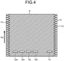
- FIG. 4 is a plan view of a schematic configuration of a ground conductor used in a radar module according to a second embodiment of the present invention.
- wedge shapes 15 are provided at the edges of the ground conductor 8, in place of the wedge shapes 14 according to the first embodiment.
- the wedge shapes 14 according to the first embodiment are angled to intersect with the antenna polarization plane Pa of 45-degree polarization at a right angle.
- the wedge shapes 15 according to the second embodiment are formed to be located vertically with respect to the edges of the ground conductor 8 to intersect with an antenna polarization plane Pa' of vertical polarization at a right angle.
- This configuration can reduce electric field components of the antenna polarization plane Pa' that are parallel to the outer periphery of the ground conductor 8, and thus reduce diffracted waves generated at the edges of the ground conductor 8, even when the vertical polarization is used in place of the 45-degree polarization.
- the present invention is not limited to the wedge shapes 14, but can use any shape as long as it has a tapered tip end, and can be a wave-curved shape, for example.
- the radar module according to the present invention can reduce diffracted waves generated at edges of a ground conductor while suppressing cost increase, and thus the radar module is suitable for a means for improving detection performances of an in-vehicle millimeter-wave radar, such as angle measurement accuracy.
Landscapes
- Engineering & Computer Science (AREA)
- Radar, Positioning & Navigation (AREA)
- Remote Sensing (AREA)
- Computer Networks & Wireless Communication (AREA)
- Physics & Mathematics (AREA)
- General Physics & Mathematics (AREA)
- Waveguide Aerials (AREA)
- Variable-Direction Aerials And Aerial Arrays (AREA)
- Radar Systems Or Details Thereof (AREA)
Description
- The present invention relates to a microstrip antenna and a radar module, and more particularly to a microstrip antenna and a radar module capable of reducing diffracted waves generated at edges of a ground conductor.
- A microstrip antenna is one of antennas used in in-vehicle millimeter-wave radars. The microstrip antenna can be manufactured by a process of etching a conductor film on an insulating substrate, and therefore downsizing and cost reduction thereof can be achieved.
- Generally, antennas used in in-vehicle millimeter-wave radars have a smaller vertical-plane beam width to only focus on target objects on the road, while having a larger horizontal-plane beam width so as to provide a wide detection range.
- As the horizontal-plane beam width increases, the antenna is likely to be affected by diffracted waves generated at edges of a ground conductor. When the diffracted waves interfere with an original received wave, a phase difference periodically varies with different horizontal angles of the beam. This variation causes ripples in an antenna gain and a phase radiation pattern, which degrades detection performances of the radar, such as angle measurement accuracy.
- As a method for solving these problems, there has been a method of reducing diffracted waves by applying or attaching a radio wave absorber on edges of an antenna substrate.
- In addition,
Patent Literature 1 discloses a technique in which a passive element is provided on edges of an antenna substrate in a microstrip antenna, and the passive element has an electrical width of one-half of a wavelength of transmitted or received electromagnetic waves, so that diffracted waves generated from a radiation element side and diffracted waves radiated from an antenna substrate edge-side portion cancel out their phases with each other. - Patent Literature 1: Japanese Patent Application Laid-open No.
H11-284429
HUFF G H ET AL: "Improvements in the Performance of Microstrip Antennas on Finite Ground Planes Through Ground Plane Edge Serrations", IEEE MICROWAVE AND WIRELESS COMPONENTS LETTERS, IEEE SERVICE CENTER, NEW YORK, NY, US, vol. 12, no. 8, 1 August 2002 (2002-08-01), XP011066886, ISSN: 1531-1309 investigated how edge serrations on a truncated ground plane affect the performance of a microstrip antenna. They found out that improvements in performance can be achieved through ground plane edge serration, which include lower cross-polarization levels, increased beamwidth, and slight impedance tuning of the fundamental and higher order modes compared to the microstrip antenna on a simple finite ground plane. - However, the above method of applying or attaching a radio wave absorber on edges of an antenna substrate not only requires preparation of extra materials, but also causes an increase in the number of processes, leading to a problem of cost increase.
- The method disclosed in
Patent Literature 1 also has problems in that a receiving antenna is designed for only a single channel, and its frequency band is limited because the width of the passive element is one-half of the wavelength. - The present invention has been achieved to solve the above problems, and an object of the present invention is to provide a microstrip antenna and a radar module capable of reducing diffracted waves generated at edges of a ground conductor, while suppressing cost increase.
- To solve the above problem and achieve an object, there is provided a radar module according to the present invention, as defined in
claim 1, which comprises an antenna substrate; a patch conductor formed on a first surface of the antenna substrate; a feeding terminal formed on the first surface of the antenna substrate; a feeding line formed on the first surface of the antenna substrate to connect the patch conductor and the feeding terminal; a ground conductor formed on a second surface of the antenna substrate to be opposed to the patch conductor; a coupling slot formed in the ground conductor and located to correspond to the position of the feeding terminal; and a circuit board located on the ground conductor opposite to the antenna substrate; wherein an edge of the ground conductor has a shape being provided in a repeated manner comprising a tapered tip end, which is angled to intersect with an antenna polarization plane, and a circuit component is mounted on the surface of the circuit board opposite to the ground conductor to supply electric power in a form of a transmission wave to the feeding terminal through the circuit board and the coupling slot. - According to the present invention, diffracted waves generated at edges of a ground conductor are reduced, while suppressing cost increase.
-
-
FIG. 1 is a plan view of a schematic configuration of a radar module according to a first embodiment of the present invention. -
FIG. 2 is a cross-sectional view taken along a line A-A' inFIG. 1 . -
FIG. 3 is a plan view of a schematic configuration of a ground conductor used in the radar module according to the first embodiment of the present invention. -
FIG. 4 is a plan view of a schematic configuration of a ground conductor used in a radar module according to a second embodiment of the present invention. - Exemplary embodiments of a microstrip antenna and a radar module according to the present invention will be explained below in detail with reference to the accompanying drawings. The present invention is not limited to the embodiments.
-
FIG. 1 is a plan view of a schematic configuration of a radar module according to a first embodiment of the present invention.FIG. 2 is a cross-sectional view taken along a line A-A' inFIG. 1 .FIG. 3 is a plan view of a schematic configuration of a ground conductor used in the radar module according to the first embodiment of the present invention. - In
FIGS. 1 to 3 ,patch conductors 2a to 2d and 3 are formed on anantenna substrate 1, while aground conductor 8 is provided on a back surface of theantenna substrate 1 to be opposed to thepatch conductors 2a to 2d and 3, thereby constituting a microstrip antenna. - In this case, the
patch conductors 2a to 2d and 3 are respectively arranged in a certain direction with a predetermined space therebetween. Thepatch conductors 2a to 2d are connected respectively to feedingterminals 4a to 4d throughfeeding lines 6a to 6d, thereby constituting a receiving antenna RN for four channels CH1 to CH4. Thepatch conductor 3 is connected to afeeding terminal 5 through afeeding line 7, thereby constituting a transmitting antenna TN. - The
ground conductor 8 is formed over the entire back surface of theantenna substrate 1. On theground conductor 8,wedge shapes 14, each having a tapered tip end, are provided along edges of theground conductor 8 in a repeated manner. In a case where an antenna polarization plane Pa forms an angle of 45 degrees, preferably thewedge shapes 14 are angled to intersect with the antenna polarization plane Pa. More preferably, thewedge shapes 14 are angled to intersect with the antenna polarization plane Pa at a right angle. -
Coupling slots 12a to 12d and 13 are formed on theground conductor 8. Thecoupling slots 12a to 12d and 13 are located to correspond to the respective positions of thefeeding terminals 4a to 4d and 5. Thecoupling slots 12a to 12d and 13 and thewedge shapes 14 are formed by patterning theground conductor 8. Particularly, thecoupling slots 12a to 12d and 13 and thewedge shapes 14 are formed all at once during a process of etching theground conductor 8. - As a material of the
antenna substrate 1, a resin substrate of glass epoxy resin, Teflon (registered trademark) resin or the like can be used, or an insulating substrate of ceramic or the like can be used. As a material of thepatch conductors 2a to 2d and 3, thefeeding lines 6a to 6d, thefeeding terminals 4a to 4d, and theground conductor 8, a thin film of metal, such as Al and Cu, can be used. Thepatch conductors 2a to 2d and 3 can be formed into a rectangular shape, a polygonal shape, a round shape, an elliptical shape or the like. -
Circuit components 11a to 11e are mounted on acircuit board 9, while a back surface of theantenna substrate 1 is bonded to theground conductor 8 via abonding layer 10. Thecircuit board 9 can be a double printed board, a multilayer printed board or a build-up board. Thecircuit components 11a to 11e can be an integrated circuit, such as an IC, or an electronic component, such as a transistor, a resistor, and a condenser. Thecircuit components 11a to 11e generate a transmission wave to be transmitted through the transmitting antenna TN and perform a receiving process for a reflected wave received through the receiving antenna RN. - The transmission wave generated on the
circuit board 9 is transmitted to thefeeding terminal 5 on theantenna substrate 1 through thecoupling slot 13. The transmission wave transmitted to thefeeding terminal 5 is then transmitted to thepatch conductor 3 through thefeeding line 7, so that electric power is supplied to the transmitting antenna TN to radiate the transmission wave into space. - When the transmission wave reaches a target, the receiving antenna RN receives a reflected wave from the target. When the reflected wave received by the receiving antenna RN reaches the
patch conductors 2a to 2d, electric power is supplied to thefeeding terminals 4a to 4d respectively through thefeeding lines 6a to 6d to transmit the reflected wave to thecircuit board 9 respectively through thecoupling slots 12a to 12d. - A receiving process based on a signal transmitted to the
circuit board 9 is performed to calculate information on an azimuth of the target, information on a relative distance to the target, information on a relative speed to the target, and the like. - In a case where a plurality of channels CH1 to CH4 are provided to the receiving antenna RN, horizontal plane scanning is performed electronically by signal processing, such as digital beamforming, thereby improving angle measurement accuracy on the horizontal plane.
- Diffracted waves are generated due to electric field components parallel to an outer periphery of the
ground conductor 8. Thewedge shapes 14 are thus provided along the each edge of theground conductor 8 in a repeated manner to reduce electric field components of the antenna polarization plane Pa that are parallel to the outer periphery of theground conductor 8, thereby reducing diffracted waves generated at the edges of theground conductor 8. As a result, it is possible to suppress interference of the diffracted waves with an original reflected wave, and thus it becomes possible to reduce ripples caused in an antenna gain and a phase radiation pattern. Therefore, detection performances of the radar, such as angle measurement accuracy, are improved even when a horizontal-plane beam width increases. - In addition, the wedge shapes 14 are formed by the process of etching the
ground conductor 8. Therefore, when the wedge shapes 14 are formed all at once simultaneously with forming thecoupling slots 12a to 12d and 13, an increase in the number of processes can be prevented while eliminating the need for extra materials such as a radio wave absorber, thereby suppressing cost increase. - In a case where a ground conductor is provided on the
circuit board 9 itself, by forming the ground conductor on thecircuit board 9 into the same shape as theground conductor 8 on theantenna substrate 1 or forming the ground conductor on thecircuit board 9 to a size small enough to prevent it from extending over the wedge shapes 14 of theground conductor 8 on theantenna substrate 1, diffracted waves can be reduced. -
FIG. 4 is a plan view of a schematic configuration of a ground conductor used in a radar module according to a second embodiment of the present invention. InFIG. 4 , in the radar module according to the second embodiment, wedge shapes 15 are provided at the edges of theground conductor 8, in place of the wedge shapes 14 according to the first embodiment. The wedge shapes 14 according to the first embodiment are angled to intersect with the antenna polarization plane Pa of 45-degree polarization at a right angle. On the other hand, the wedge shapes 15 according to the second embodiment are formed to be located vertically with respect to the edges of theground conductor 8 to intersect with an antenna polarization plane Pa' of vertical polarization at a right angle. - This configuration can reduce electric field components of the antenna polarization plane Pa' that are parallel to the outer periphery of the
ground conductor 8, and thus reduce diffracted waves generated at the edges of theground conductor 8, even when the vertical polarization is used in place of the 45-degree polarization. - The above embodiments have explained a method of providing the wedge shapes 14 along the edges of the
ground conductor 8 in a repeated manner so as to reduce diffracted waves generated at the edges of theground conductor 8. However, the present invention is not limited to the wedge shapes 14, but can use any shape as long as it has a tapered tip end, and can be a wave-curved shape, for example. - As described above, the radar module according to the present invention can reduce diffracted waves generated at edges of a ground conductor while suppressing cost increase, and thus the radar module is suitable for a means for improving detection performances of an in-vehicle millimeter-wave radar, such as angle measurement accuracy.
-
- RN
- RECEIVING ANTENNA
- TN
- TRANSMITTING ANTENNA
- 1
- ANTENNA SUBSTRATE
- 2a to 2d, 3
- PATCH CONDUCTOR
- 4a to 4d, 5
- FEEDING TERMINAL
- 6a to 6d, 7
- FEEDING LINE
- 9
- CIRCUIT BOARD
- 10
- BONDING LAYER
- 11a to 11e
- CIRCUIT COMPONENT
- 12a to 12d, 13
- COUPLING SLOT
- 14 and 15
- WEDGE SHAPE
Claims (3)
- A radar module comprising:an antenna substrate (1);a patch conductor (2a, 2b, 2c, 2d, 3) formed on a first surface of the antenna substrate (1);a feeding terminal (4a, 4b, 4c, 4d, 5) formed on the first surface of the antenna substrate (1);a feeding line (6a, 6b, 6c, 6d, 7) formed on the first surface of the antenna substrate (1) to connect the patch conductor (2a, 2b, 2c, 2d, 3) and the feeding terminal (4a, 4b, 4c, 4d, 5);a ground conductor (8) formed on a second surface of the antenna substrate (1) to be opposed to the patch conductor (2a, 2b, 2c, 2d, 3);a coupling slot (12a, 12b, 12c, 12d, 13) formed in the ground conductor (8) and located to correspond to the position of the feeding terminal (4a, 4b, 4c, 4d, 5); anda circuit board (9) located on the ground conductor (8) opposite to the antenna substrate (1);an edge of the ground conductor (8) has a shape being provided in a repeated manner, each shape comprising a tapered tip end, which is angled to intersect with an antenna polarization plane (Pa), anda circuit component (11a, 11b, 11c, 11d, 11e) is mounted on the surface of the circuit board (9) opposite to the ground conductor (8) to supply electric power in a form of a transmission wave to the feeding terminal (4a, 4b, 4c, 4d, 5) through the circuit board (9) and the coupling slot (12a, 12b, 12c, 12d, 13).
- The radar module according to claim 1, wherein the edge of the ground conductor (8) is a repeated wedge shape (14; 15).
- The radar module according to claim 2, wherein the repeated wedge shape (14; 15) is formed by patterning the ground conductor (8).
Applications Claiming Priority (2)
| Application Number | Priority Date | Filing Date | Title |
|---|---|---|---|
| JP2010024366 | 2010-02-05 | ||
| PCT/JP2011/051988 WO2011096381A1 (en) | 2010-02-05 | 2011-02-01 | Microstrip antenna and radar module |
Publications (3)
| Publication Number | Publication Date |
|---|---|
| EP2533362A1 EP2533362A1 (en) | 2012-12-12 |
| EP2533362A4 EP2533362A4 (en) | 2013-12-11 |
| EP2533362B1 true EP2533362B1 (en) | 2017-08-16 |
Family
ID=44355379
Family Applications (1)
| Application Number | Title | Priority Date | Filing Date |
|---|---|---|---|
| EP11739729.9A Not-in-force EP2533362B1 (en) | 2010-02-05 | 2011-02-01 | Microstrip antenna and radar module |
Country Status (4)
| Country | Link |
|---|---|
| US (2) | US8907848B2 (en) |
| EP (1) | EP2533362B1 (en) |
| JP (1) | JP5377671B2 (en) |
| WO (1) | WO2011096381A1 (en) |
Families Citing this family (15)
| Publication number | Priority date | Publication date | Assignee | Title |
|---|---|---|---|---|
| US9755311B2 (en) * | 2012-05-29 | 2017-09-05 | Samsung Electronics Co., Ltd. | Circularly polarized patch antennas, antenna arrays, and devices including such antennas and arrays |
| DE102014200690A1 (en) | 2014-01-16 | 2015-07-16 | Robert Bosch Gmbh | ANTENNA ARRANGEMENT, RADAR SYSTEM, VEHICLE AND METHOD |
| DE102014200692A1 (en) * | 2014-01-16 | 2015-07-16 | Robert Bosch Gmbh | PROCESS, ANTENNA ARRANGEMENT, RADAR SYSTEM AND VEHICLE |
| US10103447B2 (en) | 2014-06-13 | 2018-10-16 | Nxp Usa, Inc. | Integrated circuit package with radio frequency coupling structure |
| US9917372B2 (en) | 2014-06-13 | 2018-03-13 | Nxp Usa, Inc. | Integrated circuit package with radio frequency coupling arrangement |
| US10225925B2 (en) * | 2014-08-29 | 2019-03-05 | Nxp Usa, Inc. | Radio frequency coupling and transition structure |
| US9887449B2 (en) * | 2014-08-29 | 2018-02-06 | Nxp Usa, Inc. | Radio frequency coupling structure and a method of manufacturing thereof |
| DE102014219113A1 (en) | 2014-09-23 | 2016-03-24 | Robert Bosch Gmbh | A MIMO radar apparatus for decoupling an elevation angle and an azimuth angle of an object and a method for operating a MIMO radar apparatus |
| DE102015203454A1 (en) | 2014-10-07 | 2016-04-07 | Robert Bosch Gmbh | Method and MIMO radar apparatus for determining a positional angle of an object |
| JP6499103B2 (en) * | 2016-03-10 | 2019-04-10 | 株式会社豊田中央研究所 | Antenna device |
| US10109910B2 (en) * | 2016-05-26 | 2018-10-23 | Delphi Technologies, Inc. | Antenna device with accurate beam elevation control useable on an automated vehicle |
| CN109565304B (en) * | 2016-07-08 | 2023-04-07 | 马格纳电子系统公司 | 2D MIMO radar system for vehicle |
| JP6910830B2 (en) * | 2017-04-04 | 2021-07-28 | 株式会社デンソーテン | Planar antenna device |
| JP6896109B2 (en) | 2018-01-10 | 2021-06-30 | 三菱電機株式会社 | Waveguide microstrip line converters and antenna devices |
| KR102609138B1 (en) * | 2019-04-29 | 2023-12-05 | 삼성전기주식회사 | Printed circuit board assembly |
Family Cites Families (15)
| Publication number | Priority date | Publication date | Assignee | Title |
|---|---|---|---|---|
| US5043738A (en) | 1990-03-15 | 1991-08-27 | Hughes Aircraft Company | Plural frequency patch antenna assembly |
| US5245745A (en) * | 1990-07-11 | 1993-09-21 | Ball Corporation | Method of making a thick-film patch antenna structure |
| US5414434A (en) * | 1993-08-24 | 1995-05-09 | Raytheon Company | Patch coupled aperature array antenna |
| JPH08167812A (en) * | 1994-12-13 | 1996-06-25 | Toshiba Corp | Array antenna system |
| JPH11284429A (en) | 1998-03-27 | 1999-10-15 | Japan Radio Co Ltd | Diffraction wave suppression type microstrip antenna |
| GB2355114B (en) * | 1999-09-30 | 2004-03-24 | Harada Ind | Dual-band microstrip antenna |
| JP4135861B2 (en) * | 2001-10-03 | 2008-08-20 | 日本電波工業株式会社 | Multi-element planar antenna |
| JP2004112394A (en) | 2002-09-19 | 2004-04-08 | Hisamatsu Nakano | Microstrip antenna and radio communication apparatus using it |
| JP2005094440A (en) * | 2003-09-18 | 2005-04-07 | Tdk Corp | Antenna system and radar system |
| JP2006148688A (en) | 2004-11-22 | 2006-06-08 | Murata Mfg Co Ltd | Antenna structure and wireless radio providing the same |
| JP2007124201A (en) | 2005-10-27 | 2007-05-17 | Kyocera Corp | Antenna module |
| JP2007166115A (en) * | 2005-12-12 | 2007-06-28 | Matsushita Electric Ind Co Ltd | Antenna device |
| TWM314439U (en) * | 2006-12-08 | 2007-06-21 | Advanced Connectek Inc | Patch antenna |
| TW200835059A (en) * | 2007-02-15 | 2008-08-16 | Advanced Connectek Inc | Coupling antenna |
| US8081122B2 (en) * | 2009-06-10 | 2011-12-20 | Tdk Corporation | Folded slotted monopole antenna |
-
2011
- 2011-02-01 US US13/517,439 patent/US8907848B2/en not_active Ceased
- 2011-02-01 US US15/286,123 patent/USRE47068E1/en active Active
- 2011-02-01 JP JP2011552774A patent/JP5377671B2/en not_active Expired - Fee Related
- 2011-02-01 EP EP11739729.9A patent/EP2533362B1/en not_active Not-in-force
- 2011-02-01 WO PCT/JP2011/051988 patent/WO2011096381A1/en active Application Filing
Non-Patent Citations (1)
| Title |
|---|
| None * |
Also Published As
| Publication number | Publication date |
|---|---|
| EP2533362A1 (en) | 2012-12-12 |
| USRE47068E1 (en) | 2018-10-02 |
| US20120256795A1 (en) | 2012-10-11 |
| JP5377671B2 (en) | 2013-12-25 |
| JPWO2011096381A1 (en) | 2013-06-10 |
| WO2011096381A1 (en) | 2011-08-11 |
| US8907848B2 (en) | 2014-12-09 |
| EP2533362A4 (en) | 2013-12-11 |
Similar Documents
| Publication | Publication Date | Title |
|---|---|---|
| EP2533362B1 (en) | Microstrip antenna and radar module | |
| US10461420B2 (en) | Switchable transmit and receive phased array antenna | |
| Pal et al. | A twelve-beam steering low-profile patch antenna with shorting vias for vehicular applications | |
| US10756445B2 (en) | Switchable transmit and receive phased array antenna with high power and compact size | |
| KR100917847B1 (en) | Omni-directional planar antenna | |
| US6329950B1 (en) | Planar antenna comprising two joined conducting regions with coax | |
| US9543643B2 (en) | Antenna device and radar device | |
| US10205240B2 (en) | Shorted annular patch antenna with shunted stubs | |
| US8164535B2 (en) | Coplanar waveguide FED planar log-periodic antenna | |
| KR20180012855A (en) | The antenna element for three polarization signals | |
| US11223112B2 (en) | Inverted microstrip travelling wave patch array antenna system | |
| US20170093041A1 (en) | Coplanar waveguide transition for multi-band impedance matching | |
| JP6195080B2 (en) | Antenna device | |
| US10862212B2 (en) | Antenna device and wireless communication device | |
| CA3096346C (en) | Array antenna apparatus and communication device | |
| JP2022022348A (en) | Slot-equipped patch antenna | |
| US20190267703A1 (en) | Antenna device for a radar detector having at least two radiation directions, and motor vehicle having at least one radar detector | |
| JP2009088625A (en) | Antenna | |
| JP7060110B2 (en) | Antenna device, antenna module, communication device and radar device | |
| JP2010118778A (en) | Planar antenna and radar device | |
| EP3667821B1 (en) | Array antenna device | |
| JP2007124346A (en) | Antenna element and array type antenna | |
| JP3782278B2 (en) | Beam width control method of dual-polarized antenna | |
| KR20050075966A (en) | Omnidirectional antenna | |
| KR20190010991A (en) | Antenna |
Legal Events
| Date | Code | Title | Description |
|---|---|---|---|
| PUAI | Public reference made under article 153(3) epc to a published international application that has entered the european phase |
Free format text: ORIGINAL CODE: 0009012 |
|
| 17P | Request for examination filed |
Effective date: 20120801 |
|
| AK | Designated contracting states |
Kind code of ref document: A1 Designated state(s): AL AT BE BG CH CY CZ DE DK EE ES FI FR GB GR HR HU IE IS IT LI LT LU LV MC MK MT NL NO PL PT RO RS SE SI SK SM TR |
|
| DAX | Request for extension of the european patent (deleted) | ||
| REG | Reference to a national code |
Ref country code: HK Ref legal event code: DE Ref document number: 1175035 Country of ref document: HK |
|
| A4 | Supplementary search report drawn up and despatched |
Effective date: 20131112 |
|
| RIC1 | Information provided on ipc code assigned before grant |
Ipc: G01S 13/93 20060101ALI20131106BHEP Ipc: H01Q 1/38 20060101ALI20131106BHEP Ipc: H01Q 21/00 20060101ALI20131106BHEP Ipc: H01Q 15/14 20060101ALI20131106BHEP Ipc: G01S 7/03 20060101ALI20131106BHEP Ipc: H01Q 13/08 20060101AFI20131106BHEP Ipc: H01Q 9/04 20060101ALI20131106BHEP Ipc: H01Q 1/48 20060101ALI20131106BHEP Ipc: H01Q 1/24 20060101ALI20131106BHEP Ipc: G01S 7/02 20060101ALI20131106BHEP Ipc: H01Q 21/06 20060101ALI20131106BHEP |
|
| GRAP | Despatch of communication of intention to grant a patent |
Free format text: ORIGINAL CODE: EPIDOSNIGR1 |
|
| INTG | Intention to grant announced |
Effective date: 20170322 |
|
| GRAS | Grant fee paid |
Free format text: ORIGINAL CODE: EPIDOSNIGR3 |
|
| GRAA | (expected) grant |
Free format text: ORIGINAL CODE: 0009210 |
|
| AK | Designated contracting states |
Kind code of ref document: B1 Designated state(s): AL AT BE BG CH CY CZ DE DK EE ES FI FR GB GR HR HU IE IS IT LI LT LU LV MC MK MT NL NO PL PT RO RS SE SI SK SM TR |
|
| REG | Reference to a national code |
Ref country code: GB Ref legal event code: FG4D |
|
| REG | Reference to a national code |
Ref country code: CH Ref legal event code: EP |
|
| REG | Reference to a national code |
Ref country code: IE Ref legal event code: FG4D |
|
| REG | Reference to a national code |
Ref country code: AT Ref legal event code: REF Ref document number: 919917 Country of ref document: AT Kind code of ref document: T Effective date: 20170915 |
|
| REG | Reference to a national code |
Ref country code: DE Ref legal event code: R096 Ref document number: 602011040625 Country of ref document: DE |
|
| REG | Reference to a national code |
Ref country code: NL Ref legal event code: MP Effective date: 20170816 |
|
| REG | Reference to a national code |
Ref country code: LT Ref legal event code: MG4D |
|
| REG | Reference to a national code |
Ref country code: AT Ref legal event code: MK05 Ref document number: 919917 Country of ref document: AT Kind code of ref document: T Effective date: 20170816 |
|
| PG25 | Lapsed in a contracting state [announced via postgrant information from national office to epo] |
Ref country code: NL Free format text: LAPSE BECAUSE OF FAILURE TO SUBMIT A TRANSLATION OF THE DESCRIPTION OR TO PAY THE FEE WITHIN THE PRESCRIBED TIME-LIMIT Effective date: 20170816 Ref country code: LT Free format text: LAPSE BECAUSE OF FAILURE TO SUBMIT A TRANSLATION OF THE DESCRIPTION OR TO PAY THE FEE WITHIN THE PRESCRIBED TIME-LIMIT Effective date: 20170816 Ref country code: SE Free format text: LAPSE BECAUSE OF FAILURE TO SUBMIT A TRANSLATION OF THE DESCRIPTION OR TO PAY THE FEE WITHIN THE PRESCRIBED TIME-LIMIT Effective date: 20170816 Ref country code: FI Free format text: LAPSE BECAUSE OF FAILURE TO SUBMIT A TRANSLATION OF THE DESCRIPTION OR TO PAY THE FEE WITHIN THE PRESCRIBED TIME-LIMIT Effective date: 20170816 Ref country code: NO Free format text: LAPSE BECAUSE OF FAILURE TO SUBMIT A TRANSLATION OF THE DESCRIPTION OR TO PAY THE FEE WITHIN THE PRESCRIBED TIME-LIMIT Effective date: 20171116 Ref country code: AT Free format text: LAPSE BECAUSE OF FAILURE TO SUBMIT A TRANSLATION OF THE DESCRIPTION OR TO PAY THE FEE WITHIN THE PRESCRIBED TIME-LIMIT Effective date: 20170816 |
|
| PG25 | Lapsed in a contracting state [announced via postgrant information from national office to epo] |
Ref country code: IS Free format text: LAPSE BECAUSE OF FAILURE TO SUBMIT A TRANSLATION OF THE DESCRIPTION OR TO PAY THE FEE WITHIN THE PRESCRIBED TIME-LIMIT Effective date: 20171216 Ref country code: LV Free format text: LAPSE BECAUSE OF FAILURE TO SUBMIT A TRANSLATION OF THE DESCRIPTION OR TO PAY THE FEE WITHIN THE PRESCRIBED TIME-LIMIT Effective date: 20170816 Ref country code: GR Free format text: LAPSE BECAUSE OF FAILURE TO SUBMIT A TRANSLATION OF THE DESCRIPTION OR TO PAY THE FEE WITHIN THE PRESCRIBED TIME-LIMIT Effective date: 20171117 Ref country code: ES Free format text: LAPSE BECAUSE OF FAILURE TO SUBMIT A TRANSLATION OF THE DESCRIPTION OR TO PAY THE FEE WITHIN THE PRESCRIBED TIME-LIMIT Effective date: 20170816 Ref country code: BG Free format text: LAPSE BECAUSE OF FAILURE TO SUBMIT A TRANSLATION OF THE DESCRIPTION OR TO PAY THE FEE WITHIN THE PRESCRIBED TIME-LIMIT Effective date: 20171116 Ref country code: PL Free format text: LAPSE BECAUSE OF FAILURE TO SUBMIT A TRANSLATION OF THE DESCRIPTION OR TO PAY THE FEE WITHIN THE PRESCRIBED TIME-LIMIT Effective date: 20170816 Ref country code: RS Free format text: LAPSE BECAUSE OF FAILURE TO SUBMIT A TRANSLATION OF THE DESCRIPTION OR TO PAY THE FEE WITHIN THE PRESCRIBED TIME-LIMIT Effective date: 20170816 |
|
| PG25 | Lapsed in a contracting state [announced via postgrant information from national office to epo] |
Ref country code: DK Free format text: LAPSE BECAUSE OF FAILURE TO SUBMIT A TRANSLATION OF THE DESCRIPTION OR TO PAY THE FEE WITHIN THE PRESCRIBED TIME-LIMIT Effective date: 20170816 Ref country code: RO Free format text: LAPSE BECAUSE OF FAILURE TO SUBMIT A TRANSLATION OF THE DESCRIPTION OR TO PAY THE FEE WITHIN THE PRESCRIBED TIME-LIMIT Effective date: 20170816 Ref country code: CZ Free format text: LAPSE BECAUSE OF FAILURE TO SUBMIT A TRANSLATION OF THE DESCRIPTION OR TO PAY THE FEE WITHIN THE PRESCRIBED TIME-LIMIT Effective date: 20170816 |
|
| REG | Reference to a national code |
Ref country code: DE Ref legal event code: R097 Ref document number: 602011040625 Country of ref document: DE |
|
| PG25 | Lapsed in a contracting state [announced via postgrant information from national office to epo] |
Ref country code: IT Free format text: LAPSE BECAUSE OF FAILURE TO SUBMIT A TRANSLATION OF THE DESCRIPTION OR TO PAY THE FEE WITHIN THE PRESCRIBED TIME-LIMIT Effective date: 20170816 Ref country code: SK Free format text: LAPSE BECAUSE OF FAILURE TO SUBMIT A TRANSLATION OF THE DESCRIPTION OR TO PAY THE FEE WITHIN THE PRESCRIBED TIME-LIMIT Effective date: 20170816 Ref country code: SM Free format text: LAPSE BECAUSE OF FAILURE TO SUBMIT A TRANSLATION OF THE DESCRIPTION OR TO PAY THE FEE WITHIN THE PRESCRIBED TIME-LIMIT Effective date: 20170816 Ref country code: EE Free format text: LAPSE BECAUSE OF FAILURE TO SUBMIT A TRANSLATION OF THE DESCRIPTION OR TO PAY THE FEE WITHIN THE PRESCRIBED TIME-LIMIT Effective date: 20170816 |
|
| PLBE | No opposition filed within time limit |
Free format text: ORIGINAL CODE: 0009261 |
|
| STAA | Information on the status of an ep patent application or granted ep patent |
Free format text: STATUS: NO OPPOSITION FILED WITHIN TIME LIMIT |
|
| 26N | No opposition filed |
Effective date: 20180517 |
|
| PG25 | Lapsed in a contracting state [announced via postgrant information from national office to epo] |
Ref country code: SI Free format text: LAPSE BECAUSE OF FAILURE TO SUBMIT A TRANSLATION OF THE DESCRIPTION OR TO PAY THE FEE WITHIN THE PRESCRIBED TIME-LIMIT Effective date: 20170816 |
|
| REG | Reference to a national code |
Ref country code: CH Ref legal event code: PL |
|
| PG25 | Lapsed in a contracting state [announced via postgrant information from national office to epo] |
Ref country code: MC Free format text: LAPSE BECAUSE OF FAILURE TO SUBMIT A TRANSLATION OF THE DESCRIPTION OR TO PAY THE FEE WITHIN THE PRESCRIBED TIME-LIMIT Effective date: 20170816 |
|
| REG | Reference to a national code |
Ref country code: IE Ref legal event code: MM4A |
|
| REG | Reference to a national code |
Ref country code: BE Ref legal event code: MM Effective date: 20180228 |
|
| PG25 | Lapsed in a contracting state [announced via postgrant information from national office to epo] |
Ref country code: CH Free format text: LAPSE BECAUSE OF NON-PAYMENT OF DUE FEES Effective date: 20180228 Ref country code: LI Free format text: LAPSE BECAUSE OF NON-PAYMENT OF DUE FEES Effective date: 20180228 Ref country code: LU Free format text: LAPSE BECAUSE OF NON-PAYMENT OF DUE FEES Effective date: 20180201 |
|
| REG | Reference to a national code |
Ref country code: FR Ref legal event code: ST Effective date: 20181031 |
|
| PG25 | Lapsed in a contracting state [announced via postgrant information from national office to epo] |
Ref country code: IE Free format text: LAPSE BECAUSE OF NON-PAYMENT OF DUE FEES Effective date: 20180201 |
|
| PG25 | Lapsed in a contracting state [announced via postgrant information from national office to epo] |
Ref country code: BE Free format text: LAPSE BECAUSE OF NON-PAYMENT OF DUE FEES Effective date: 20180228 Ref country code: FR Free format text: LAPSE BECAUSE OF NON-PAYMENT OF DUE FEES Effective date: 20180228 |
|
| PGFP | Annual fee paid to national office [announced via postgrant information from national office to epo] |
Ref country code: DE Payment date: 20190122 Year of fee payment: 9 Ref country code: GB Payment date: 20190130 Year of fee payment: 9 |
|
| PG25 | Lapsed in a contracting state [announced via postgrant information from national office to epo] |
Ref country code: MT Free format text: LAPSE BECAUSE OF NON-PAYMENT OF DUE FEES Effective date: 20180201 |
|
| PG25 | Lapsed in a contracting state [announced via postgrant information from national office to epo] |
Ref country code: TR Free format text: LAPSE BECAUSE OF FAILURE TO SUBMIT A TRANSLATION OF THE DESCRIPTION OR TO PAY THE FEE WITHIN THE PRESCRIBED TIME-LIMIT Effective date: 20170816 |
|
| PG25 | Lapsed in a contracting state [announced via postgrant information from national office to epo] |
Ref country code: PT Free format text: LAPSE BECAUSE OF FAILURE TO SUBMIT A TRANSLATION OF THE DESCRIPTION OR TO PAY THE FEE WITHIN THE PRESCRIBED TIME-LIMIT Effective date: 20170816 Ref country code: HU Free format text: LAPSE BECAUSE OF FAILURE TO SUBMIT A TRANSLATION OF THE DESCRIPTION OR TO PAY THE FEE WITHIN THE PRESCRIBED TIME-LIMIT; INVALID AB INITIO Effective date: 20110201 |
|
| PG25 | Lapsed in a contracting state [announced via postgrant information from national office to epo] |
Ref country code: MK Free format text: LAPSE BECAUSE OF NON-PAYMENT OF DUE FEES Effective date: 20170816 Ref country code: CY Free format text: LAPSE BECAUSE OF FAILURE TO SUBMIT A TRANSLATION OF THE DESCRIPTION OR TO PAY THE FEE WITHIN THE PRESCRIBED TIME-LIMIT Effective date: 20170816 Ref country code: HR Free format text: LAPSE BECAUSE OF FAILURE TO SUBMIT A TRANSLATION OF THE DESCRIPTION OR TO PAY THE FEE WITHIN THE PRESCRIBED TIME-LIMIT Effective date: 20170816 |
|
| PG25 | Lapsed in a contracting state [announced via postgrant information from national office to epo] |
Ref country code: AL Free format text: LAPSE BECAUSE OF FAILURE TO SUBMIT A TRANSLATION OF THE DESCRIPTION OR TO PAY THE FEE WITHIN THE PRESCRIBED TIME-LIMIT Effective date: 20170816 |
|
| REG | Reference to a national code |
Ref country code: DE Ref legal event code: R119 Ref document number: 602011040625 Country of ref document: DE |
|
| GBPC | Gb: european patent ceased through non-payment of renewal fee |
Effective date: 20200201 |
|
| PG25 | Lapsed in a contracting state [announced via postgrant information from national office to epo] |
Ref country code: GB Free format text: LAPSE BECAUSE OF NON-PAYMENT OF DUE FEES Effective date: 20200201 Ref country code: DE Free format text: LAPSE BECAUSE OF NON-PAYMENT OF DUE FEES Effective date: 20200901 |