EP3985881A1 - Wideband radio-frequency transceiver front-end and operation method thereof - Google Patents
Wideband radio-frequency transceiver front-end and operation method thereof Download PDFInfo
- Publication number
- EP3985881A1 EP3985881A1 EP20201999.8A EP20201999A EP3985881A1 EP 3985881 A1 EP3985881 A1 EP 3985881A1 EP 20201999 A EP20201999 A EP 20201999A EP 3985881 A1 EP3985881 A1 EP 3985881A1
- Authority
- EP
- European Patent Office
- Prior art keywords
- power amplifier
- transceiver front
- controller
- matching network
- gate
- Prior art date
- Legal status (The legal status is an assumption and is not a legal conclusion. Google has not performed a legal analysis and makes no representation as to the accuracy of the status listed.)
- Granted
Links
Images


Classifications
-
- H—ELECTRICITY
- H04—ELECTRIC COMMUNICATION TECHNIQUE
- H04B—TRANSMISSION
- H04B1/00—Details of transmission systems, not covered by a single one of groups H04B3/00 - H04B13/00; Details of transmission systems not characterised by the medium used for transmission
- H04B1/02—Transmitters
- H04B1/04—Circuits
- H04B1/0458—Arrangements for matching and coupling between power amplifier and antenna or between amplifying stages
-
- H—ELECTRICITY
- H03—ELECTRONIC CIRCUITRY
- H03F—AMPLIFIERS
- H03F1/00—Details of amplifiers with only discharge tubes, only semiconductor devices or only unspecified devices as amplifying elements
- H03F1/42—Modifications of amplifiers to extend the bandwidth
-
- H—ELECTRICITY
- H03—ELECTRONIC CIRCUITRY
- H03F—AMPLIFIERS
- H03F3/00—Amplifiers with only discharge tubes or only semiconductor devices as amplifying elements
- H03F3/20—Power amplifiers, e.g. Class B amplifiers, Class C amplifiers
- H03F3/24—Power amplifiers, e.g. Class B amplifiers, Class C amplifiers of transmitter output stages
- H03F3/245—Power amplifiers, e.g. Class B amplifiers, Class C amplifiers of transmitter output stages with semiconductor devices only
-
- H—ELECTRICITY
- H04—ELECTRIC COMMUNICATION TECHNIQUE
- H04B—TRANSMISSION
- H04B1/00—Details of transmission systems, not covered by a single one of groups H04B3/00 - H04B13/00; Details of transmission systems not characterised by the medium used for transmission
- H04B1/06—Receivers
- H04B1/16—Circuits
- H04B1/18—Input circuits, e.g. for coupling to an antenna or a transmission line
-
- H—ELECTRICITY
- H04—ELECTRIC COMMUNICATION TECHNIQUE
- H04B—TRANSMISSION
- H04B1/00—Details of transmission systems, not covered by a single one of groups H04B3/00 - H04B13/00; Details of transmission systems not characterised by the medium used for transmission
- H04B1/38—Transceivers, i.e. devices in which transmitter and receiver form a structural unit and in which at least one part is used for functions of transmitting and receiving
- H04B1/40—Circuits
-
- H—ELECTRICITY
- H04—ELECTRIC COMMUNICATION TECHNIQUE
- H04B—TRANSMISSION
- H04B1/00—Details of transmission systems, not covered by a single one of groups H04B3/00 - H04B13/00; Details of transmission systems not characterised by the medium used for transmission
- H04B1/38—Transceivers, i.e. devices in which transmitter and receiver form a structural unit and in which at least one part is used for functions of transmitting and receiving
- H04B1/40—Circuits
- H04B1/44—Transmit/receive switching
-
- H—ELECTRICITY
- H03—ELECTRONIC CIRCUITRY
- H03F—AMPLIFIERS
- H03F2200/00—Indexing scheme relating to amplifiers
- H03F2200/36—Indexing scheme relating to amplifiers the amplifier comprising means for increasing the bandwidth
-
- H—ELECTRICITY
- H03—ELECTRONIC CIRCUITRY
- H03F—AMPLIFIERS
- H03F2200/00—Indexing scheme relating to amplifiers
- H03F2200/451—Indexing scheme relating to amplifiers the amplifier being a radio frequency amplifier
Definitions
- the invention relates to a radio-frequency (RF) transceiver operating at millimeter waves or Terahertz frequencies, especially to a wideband front-end circuit for wireless communication in time-division duplexing (TDD) systems.
- RF radio-frequency
- noise figure acts as the key specification, especially while the transceiver is in receiving mode, which affects the system performance significantly.
- wide operational bandwidth is available for wireless communication at millimeter waves and Terahertz frequencies.
- it is hard to keep a low NF for the entire wide operation bandwidth.
- a low NF of the front-end circuit is required within a wide operation bandwidth.
- the document US 2020/0083924 A1 shows a transmit receive switch system, where a symmetric ⁇ /4 transmission line switching topology is incorporated in order to perform impedance matching on both transmitter and receiver ends.
- a symmetric ⁇ /4 transmission line switching topology is incorporated in order to perform impedance matching on both transmitter and receiver ends.
- the presence of passive components at the transmission path disadvantageously leads to higher insertion loss, especially at higher frequencies (Terahertz), which results in lower output power from the power amplifier at the transmitter end.
- an object of the invention is to provide a wideband RF transceiver front-end and an operation method for the same, which can overcome the aforementioned limitations.
- the object is solved by the features of the first independent claim for the wideband RF transceiver front-end and by the features of the second independent claim for the method.
- the dependent claims contain further developments.
- a wideband radio-frequency transceiver front-end includes an antenna port and a transmission path coupled to the antenna port comprising a power amplifier and a first matching network.
- the transceiver front-end further includes a reception path coupled to the antenna port comprising a low noise amplifier and a second matching network.
- the transceiver front-end includes an impedance inverter coupled in-between the antenna port and the second matching network.
- the transceiver front-end includes a controller comprising switching arrangement for a gate and a drain of the power amplifier.
- the controller is configured to initiate a first reception mode by connecting the gate of the power amplifier to ground and by connecting the drain of the power amplifier to a supply voltage. Therefore, the inventive solution eliminates the necessity of having passive elements at the transmission path by introducing additional switching functionalities at the power amplifier. Especially, while receiving, the inventive solution facilitates a first mode of operation in which the transmitter power amplifier is not completely switched off, instead configures the LC resonance of the coil of the first matching network and the equivalent drain capacitance of transistors. Consequently, while receiving, the impedance looking into the transmission path from the receiving path changes according to the operation frequency, which advantageously reduces the NF.
- the controller is further configured to initiate a second reception mode by connecting the gate of the power amplifier to a bias voltage and by connecting the drain of the power amplifier to ground. Therefore, while receiving, the inventive solution facilitates a second mode of operation that further manipulates the impedance transformation at the transmission path.
- the combined operation of the first reception mode and the second reception mode advantageously facilitates a low NF for a wide operation bandwidth.
- the transceiver front-end further comprises a shunt switch coupled to the low noise amplifier.
- the controller is further configured to initiate a transmission mode by switching on the shunt switch, thereby creating a low impedance short across the low noise amplifier.
- the controller is further configured to connect the gate of the power amplifier to a bias voltage and the drain of the power amplifier to the supply voltage during the transmission mode.
- the shunt switch is placed across the input of the low noise amplifier, i.e., between the second matching network and the input terminals of the low noise amplifier.
- This provides an Electrostatic Discharge (ESD) protection topology, since any potential ESD-event current from the antenna port will be led to ground through the matching networks.
- ESD Electrostatic Discharge
- the controller is further configured to cause the shunt switch to be off during the first reception mode and/or the second reception mode.
- the controller may also be configured to control timing of the shunt switch when transferring from the transmission mode to the first and/or second reception mode.
- the controller further comprises a switching arrangement for a gate of the low noise amplifier.
- the controller is further configured to connect the gate of the low noise amplifier to ground during the transmission mode.
- the controller is further configured to connect the gate of the low noise amplifier to a bias voltage during the first reception mode and/or the second reception mode.
- the second matching network is further configured to not only transform impedance but also to compensate any parasitic associated with the shunt switch (both on and off states) as well as for the transistors of the low noise amplifier.
- the impedance inverter is preferably a quarter-wavelength ( ⁇ /4) transmission line, configured to perform a short-to-open impedance transformation.
- the impedance inverter can be implemented as a transmission line that has a length of less than ⁇ /4 in order to match the additional impedance contribution of the second matching network.
- the controller is further configured to initiate the first reception mode for a frequency band over an operating frequency band greater than or less than or equal to a center frequency. Additionally or alternately, the controller is further configured to initiate the second reception mode for a frequency band over the operating frequency band greater than or less than or equal to the center frequency.
- the matching network parameters essentially dictate the modes of operation with respect to the operating frequency, i.e. whether it is required to initiate the first or second reception mode above or below the center frequency of the whole operation bandwidth. However, operating at the center frequency is the optimum case.
- the operating frequency band is in the range of millimeter band, preferably up to Terahertz frequency band.
- the operating frequency band can be the whole D-band, where the center frequency can be at or around 150GHz.
- a wide operation bandwidth is incorporated and by means of the first and second reception modes, a low NF is maintained throughout the operation bandwidth.
- the first matching network and the second matching network are transformer based matching networks, preferably transformer-type baluns.
- the first impedance matching network and/or the second impedance matching network are not limited to transformer-type baluns.
- the second matching network can be implemented as a LC-based matching network, i.e. the low noise amplifier is configured as single-ended version.
- a method for operating a wideband radio-frequency transceiver front-end comprises the step of providing a transmission path, comprising a power amplifier and a first matching network, coupled to an antenna port.
- the method further comprises the step of providing a reception path, comprising a low noise amplifier and a second matching network, coupled to the antenna port.
- the method comprises the step of providing an impedance inverter coupled in-between the antenna port and the second matching network.
- the method comprises the step of initiating a first reception mode by connecting a gate of the power amplifier to ground and by connecting a drain of the power amplifier to a supply voltage.
- the method further comprises the step of initiating a second reception mode by connecting the gate of the power amplifier to a bias voltage and by connecting the drain of the power amplifier to ground. Therefore, the inventive solution provides a transceiver front-end that operates over a wide operation bandwidth, while facilitating higher output power and higher power efficiency for the transmitter power amplifier and further maintains a low NF for the entire operation bandwidth.
- the method further comprises the step of initiating a transmission mode by switching on a shunt switch coupled to the low noise amplifier and further by connecting the gate of the power amplifier to a bias voltage and the drain of the power amplifier to the supply voltage.
- a provision for ESD protection is also incorporated.
- the method further comprises the step of initiating the first reception mode for a frequency band greater than or less than or equal to a center frequency and initiating the second reception mode for a frequency band greater than or less than or equal to the center frequency over an operating frequency band. Therefore, a flexible operation for the first and second reception modes is incorporated with respect to the operating bandwidth.
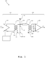
- the transceiver front-end 100 comprises an antenna port 101 and an antenna or antenna array 102 coupled at the antenna port 101, which is terminated to ground 104.
- the parasitic for termination is hereby illustrated as a pad capacitance 103 (e.g., a flip chip pad capacitance).
- the antenna or antenna array 102 preferably operates at millimeter wave as well as at sub-millimeter wave.
- the transceiver front-end 100 further comprises a transmission path 110 that is coupled to the antenna port 101.
- Said transmission path 110 comprises a transmitter amplifier or transmitter power amplifier or power amplifier 111 and a first transformer based impedance matching network 113.
- the power amplifier 111 receives baseband signal 112 from a baseband generator (not shown) and performs the final stage amplification to generate the transmission signal, which is transmitted through the antenna 102 during transmission. Specifically, the power amplifier 111 operates in differential mode, where the received baseband and the amplified output signals are differential type signals.
- the output of the power amplifier 111 is coupled to the first coil 114 of the first matching network 113.
- the second coil 116 of the first matching network 113 is coupled to the antenna port 101.
- the transceiver front-end 100 further comprises a reception path 120 that is coupled to the antenna port 101.
- Said reception path comprises a receiver amplifier or receiver low noise amplifier or low noise amplifier 121, a second transformer based impedance matching network 123 and an impedance inverter 125.
- the low noise amplifier 121 amplifies the received signal, which is received through the antenna 102 during reception and provides amplified received signal 122 at its output. Specifically, the low noise amplifier 121 operates in differential mode, where the received signal and the amplified received signal are differential type signals.
- the input terminals of the low noise amplifier i.e., the gates of the transistors, are coupled to a switch 127 in shunt, hereinafter referred as a shunt switch 127. Said terminals are further coupled to the first coil 124 of the second matching network 123.
- the second coil 126 of the second matching network 123 is coupled to an impedance inverter, preferably realized by a transmission line having a length shorter than one quarter-wavelength.
- the impedance inverter 125 is coupled in-between the antenna port 101 and the second coil 126 of the second matching network 123.
- the second matching network 123 is not limited to a transformer based matching network, since a LC based matching network can also be implemented, where the low noise amplifier 121 will perform single-ended operation.
- the transceiver front-end 100 further comprises a controller 105 that operates on the shunt switch 127, therefore is configured to cause the shunt switch 127 to be on and off as needed for transmission and reception operations, respectively.
- the controller 105 further includes provisions for different voltage levels, i.e., the supply voltage Vdd, the gate bias voltage Vg and its variances, and ground potential (0V).
- the controller 105 comprises supply switch or switches in order to perform the switching of potentials ranging from the ground potential (0V) to the supply voltage (Vdd).
- the switch control logic can be transmitted via control signals (depicted as dashed lines) from the controller 105 to the respective paths 110, 120.
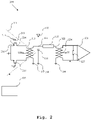
- FIG. 2 an exemplary embodiment of the transceiver front-end in transmission mode 200, hereinafter referred as TX-mode, according to the first aspect of the invention is illustrated.
- the power amplifier 111 illustrated in detail, showing the differential arrangement of two transistors 211, 213 with their respective gate 212, drain 214 and source 216 terminals.
- the topology shows only one transistor per path, it is conceivable that the topology can be extended to a larger number of stacked-transistor power amplifier topology.
- the power amplifier 111 can also be implemented as a cross-capacitive coupled common source power amplifier.
- the controller 105 In order to initiate the TX-mode 200, the controller 105 causes the shunt switch 127 to be on, thereby creating a low impedance short across the inputs of the low noise amplifier 121 (i.e. across the first coil 124 of the second matching network 123). In addition, the controller 105 connects the gates 224 of the low noise amplifier 121 (i.e., the transistor switches of the low noise amplifier 121) to ground 104 (0V). This results in the deactivation of the reception path 120 while keeping the transmission path 110 active.
- the second matching network 123 advantageously allows avoiding the termination of the inactive reception path directly to ground 104.
- the second matching network 123 also takes into account the parasitic associated with the shunt switch 127 when it is switched on.
- the low impedance short caused by the shunt switch 127 across the first coil 124 of the second matching network 123 is transformed into a high impedance by the impedance inverter 125, seen at the antenna node 101 from the perspective of the power amplifier 111.
- the impedance inverter 125 is, for instance, a transmission line that has a length of slightly less than ⁇ /4, which takes into account the additional impedance contribution of the second matching network 123.
- the combined operation of the impedance inverter 125 and the second matching network 123 provides a combined impedance transformation of ⁇ /4.
- the high impedance can be achieved based on resonance between cumulative capacitance of transmission line and pad capacitances and the transmission line impedance of the impedance inverter 125.
- the controller 105 connects the drain of the power amplifier 111, especially the drains 214 of the transistors 211, 213 to a supply voltage Vdd.
- the controller 105 further connects the gate of the power amplifier 111, especially the gates 212 of the transistors to a bias voltage Vg.
- the voltage switching is performed at a center tap of the first coil 114 of the first matching network 113 and at a center tap of the first coil 124 of the second matching network 123 for the power amplifier 111 and the low noise amplifier 121, respectively.
- a first exemplary embodiment of the transceiver front-end in reception mode 300 hereinafter referred as PA-SW-OFF, according to the first aspect of the invention is illustrated.
- the controller 105 connects the gate of the power amplifier 111, especially the gates 212 of the transistors to ground 104 (0V). Furthermore, the controller 105 connects the drain of the power amplifier 111, especially the drains 214 of the transistors to the supply voltage Vdd. This effectively disables the power amplifier 111 to a high impedance state, which provides adequate isolation from the antenna port 101, thereby deactivating the transmission path 110.
- the controller 105 causes the shunt switch 127 to be off, which presents an off switch capacitance across the low noise amplifier 121 (i.e., across the first coil 124 of the second matching network 123).
- the controller 105 connects the gate of the low noise amplifier 121, especially the gates 224 of the transistors to the bias voltage Vg, thereby activating the reception path 120.
- the second matching network 123 further takes into account the parasitic associated with the shunt switch 127 when it is switched off.
- a second exemplary embodiment of the transceiver front-end 400 in reception mode according to the first aspect of the invention is illustrated.
- the controller 105 connects the gate of the power amplifier 111, especially the gates 212 of the transistors to a bias voltage Vsw.
- Said bias voltage Vsw can be lower or higher than the nominal bias voltage Vg.
- the bias voltage Vsw can be within the range of the nominal bias voltage Vg and the supply voltage Vdd. Alternately, said bias voltage Vsw is as high as the supply voltage Vdd.
- the bias voltage Vsw is sufficiently high in order to enable the transistors of the power amplifier 111 to stay in the ohmic region.
- the controller 105 connects the drain of the power amplifier 111, especially the drains 214 of the transistors to the ground 104 (0V).
- the gate biasing voltages of the power amplifier 111 are set to a certain value to turn on the transistors while grounding the supply voltage of the power amplifier 111.
- the first matching network 113 performs a short to open impedance transform, i.e., transforming the low impedance of the power amplifier 111 operating as a low impedance shunt switch into a high impedance. This provides adequate isolation from the antenna port 101, thereby deactivating the transmission path 110.
- the controller 105 causes the shunt switch 127 to be off, which presents an off switch capacitance across the low noise amplifier 121 (i.e., across the first coil 124 of the second matching network 123).
- the controller 105 connects the gate of the low noise amplifier 121, especially the gates 224 of the transistors to the bias voltage Vg, thereby activating the reception path 120.
- the second matching network 123 further takes into account the parasitic associated with the shunt switch 127 when it is switched off.
- the power amplifier 111 operates as a large amplifying device, while the low impedance short across the low noise amplifier 121 is converted into a high impedance in order to achieve a high transmission efficiency.
- the power amplifier 111 is disabled to a high impedance state in order to provide good isolation and hence low NF in the receiver topology.
- the PA-SW-ON 400 the power amplifier 111 is disabled to a low impedance shunt while converting the low impedance into a high impedance at the antenna port 101. This further provides adequate isolation from the antenna port 101 and hence low NF in the receiver topology.
- the PA-SW-OFF 300 and the PA-SW-ON 400 modes are implemented at different frequencies and they do not coexist at one frequency.
- exemplary NF simulations for the PA-SW-OFF 300 and PA-SW-ON 400 are illustrated.
- the horizontal axis denotes the operating frequency range in Gigahertz and the vertical axis denotes the NF in decibels.
- the operation frequency range correspond to the whole D-band, as illustrated herein, where the center frequency is at or around 150GHz.
- the operation frequency band can be in the range of millimeter wave as well as sub-millimeter wave range.
- three observation frequencies are selected in order to demonstrate the NF fluctuation over the frequency range.
- a first observation frequency is selected at 135GHz
- a second observation frequency is selected around the center frequency at 149GHz
- a third observation frequency is selected at 165GHz.
- the solid line represents the PA-SW-OFF 300 mode and the dashed line represents the PA-SW-ON 400 mode.
- the receiver NF 501 for PA-SW-OFF is approximately 5.05dB and the receiver NF 502 for PA-SW-ON is approximately 6.35dB.
- the receiver NF 503 for PA-SW-OFF is approximately 5.81dB and the receiver NF 504 for PA-SW-ON is approximately 5.81dB.
- the receiver NF 505 for PA-SW-OFF is approximately 9.22dB and the receiver NF 506 for PA-SW-ON is approximately 5.93dB.
- the NF degrades drastically for PA-SW-OFF as the operating frequency increases, whereas the NF is somewhat constant for PA-SW-ON over the whole frequency range.
- the NF performance for PA-SW-OFF is superior to the NF performance for PA-SW-ON by approximately 1dB. Therefore, the inventive solution incorporates both PA-SW-OFF and PA-SW-ON modes over the whole operation bandwidth, where one mode is active for frequencies lower that the center frequency and the other mode is active for frequencies higher that the center frequency.
- the NF performance of PA-SW-OFF is superior to PA-SW-ON for frequencies lower than the center frequency, therefore the PA-SW-OFF is initiated for frequencies lower than the center frequency. Further, the PA-SW-ON is initiated for frequencies higher than the center frequency, since the NF performance of PA-SW-ON is superior to the PA-SW-OFF for frequencies higher than the center frequencies.
- the initiation of both PA-SW-OFF and PA-SW-OFF with respect to their operating frequency range largely depends on the matching network parameters.
- FIG. 6 shows an exemplary test bench environment simulating NF degradation due to transmission path loss.
- Fig. 6 shows an adopted test bench for simulating the NF degradation due to transmission path loss.
- the simulated impedance ZM looking into the transmission path and NF over frequencies are illustrated in Fig. 7 .
- the operation frequency range illustrated herein corresponds to the whole D-band, where the center frequency is at 150GHz. However, it is conceivable that the illustration is to exemplify the NF degradation and the inventive solution is not limited to the D-band only.
- the operation frequency band can be in the range of millimeter wave as well as sub-millimeter wave range.
- the horizontal axis denotes the operating frequency range in Gigahertz.
- the vertical axis for the simulation at top denotes the real ZM in ohm.
- the vertical axis for the simulation at middle denotes the imaginary ZM in ohm.
- the vertical axis for the simulation at bottom denotes the NF in decibels.
- three observation frequencies are selected over the frequency range. A first observation frequency is selected at 135GHz, a second observation frequency is selected at the center frequency at 150GHz and a third observation frequency is selected at 165GHz.
- the solid line represents the PA-SW-OFF 300 mode and the dashed line represents the PA-SW-ON 400 mode.
- the real value of ZM at 135GHz is around 65ohm and 98ohm for PA-SW-OFF and PA-SW-ON, respectively.
- the real value of ZM at 150GHz is around 58ohm and 60ohm for PA-SW-OFF and PA-SW-ON, respectively.
- the real value of ZM at 165GHz is around 113ohm and 46ohm for PA-SW-OFF and PA-SW-ON, respectively.
- the imaginary value of ZM at 135GHz is around -30ohm and -72ohm for PA-SW-OFF and PA-SW-ON, respectively.
- the imaginary value of ZM at 150GHz is around 2ohm and -49ohm for PA-SW-OFF and PA-SW-ON, respectively.
- the imaginary value of ZM at 165GHz is around 17ohm and -30ohm for PA-SW-OFF and PA-SW-ON, respectively.
- the combined ZM of PA-SW-OFF and PA-SW-ON modes over the whole operating frequency range has less variations that the individual ZM in PA-SW-OFF and PA-SW-ON mode, respectively.
- the matching networks, especially the second matching network 123, will be benefited significantly by the proposed technique.
- the NF at 135GHz is around 1.1dB and 1.6dB for PA-SW-OFF and PA-SW-ON, respectively.
- the NF at 150GHz is around 1.6dB and 1.5dB for PA-SW-OFF and PA-SW-ON, respectively.
- the NF at 165GHz is around 3.4dB and 1.4dB for PA-SW-OFF and PA-SW-ON, respectively.
- a transmission path is provided that comprises a power amplifier and a first matching network, where the transmission path is coupled to an antenna port.
- a reception path is provided that comprises a low noise amplifier and a second matching network, where the reception path is coupled to the antenna port.
- an impedance inverter is provided that is coupled in-between the antenna port and the second matching network.
- a first reception mode is initiated by connecting a gate of the power amplifier to ground and by connecting a drain of the power amplifier to a supply voltage.
- a second reception mode is initiated by connecting the gate of the power amplifier to a bias voltage and by connecting the drain of the power amplifier to ground.
- a transmission mode is initiated by switching on a shunt switch coupled to the low noise amplifier and further by connecting the gate of the power amplifier to a bias voltage and the drain of the power amplifier to the supply voltage.
- the embodiments of the present invention can be implemented by hardware, software, or any combination thereof.
- Various embodiments of the present invention may be implemented by one or more application specific integrated circuits (ASICs), digital signal processors (DSPs), digital signal processing devices (DSPDs), programmable logic devices (PLDs), field programmable gate arrays (FPGAs), processors, controllers, microcontrollers, microprocessors, or the like.
- ASICs application specific integrated circuits
- DSPs digital signal processors
- DSPDs digital signal processing devices
- PLDs programmable logic devices
- FPGAs field programmable gate arrays
- processors controllers, microcontrollers, microprocessors, or the like.
Landscapes
- Engineering & Computer Science (AREA)
- Computer Networks & Wireless Communication (AREA)
- Signal Processing (AREA)
- Power Engineering (AREA)
- Amplifiers (AREA)
- Transceivers (AREA)
Abstract
Description
- The invention relates to a radio-frequency (RF) transceiver operating at millimeter waves or Terahertz frequencies, especially to a wideband front-end circuit for wireless communication in time-division duplexing (TDD) systems.
- Generally, in a TDD RF transceiver front-end, noise figure (NF) acts as the key specification, especially while the transceiver is in receiving mode, which affects the system performance significantly. Presently, wide operational bandwidth is available for wireless communication at millimeter waves and Terahertz frequencies. However, it is hard to keep a low NF for the entire wide operation bandwidth. In order to maintain good RF performance for TDD RF transceiver front-end at millimeter waves, a low NF of the front-end circuit is required within a wide operation bandwidth.
- For example, the document
US 2020/0083924 A1 shows a transmit receive switch system, where a symmetric λ/4 transmission line switching topology is incorporated in order to perform impedance matching on both transmitter and receiver ends. However, the presence of passive components at the transmission path disadvantageously leads to higher insertion loss, especially at higher frequencies (Terahertz), which results in lower output power from the power amplifier at the transmitter end. - Accordingly, an object of the invention is to provide a wideband RF transceiver front-end and an operation method for the same, which can overcome the aforementioned limitations.
- The object is solved by the features of the first independent claim for the wideband RF transceiver front-end and by the features of the second independent claim for the method. The dependent claims contain further developments.
- According to a first aspect of the invention, a wideband radio-frequency transceiver front-end is provided. The transceiver front-end includes an antenna port and a transmission path coupled to the antenna port comprising a power amplifier and a first matching network. The transceiver front-end further includes a reception path coupled to the antenna port comprising a low noise amplifier and a second matching network. Furthermore, the transceiver front-end includes an impedance inverter coupled in-between the antenna port and the second matching network. Moreover, the transceiver front-end includes a controller comprising switching arrangement for a gate and a drain of the power amplifier.
- In this context, the controller is configured to initiate a first reception mode by connecting the gate of the power amplifier to ground and by connecting the drain of the power amplifier to a supply voltage. Therefore, the inventive solution eliminates the necessity of having passive elements at the transmission path by introducing additional switching functionalities at the power amplifier. Especially, while receiving, the inventive solution facilitates a first mode of operation in which the transmitter power amplifier is not completely switched off, instead configures the LC resonance of the coil of the first matching network and the equivalent drain capacitance of transistors. Consequently, while receiving, the impedance looking into the transmission path from the receiving path changes according to the operation frequency, which advantageously reduces the NF.
- According to a first preferred implementation form of said first aspect of the invention, the controller is further configured to initiate a second reception mode by connecting the gate of the power amplifier to a bias voltage and by connecting the drain of the power amplifier to ground. Therefore, while receiving, the inventive solution facilitates a second mode of operation that further manipulates the impedance transformation at the transmission path. Hence, the combined operation of the first reception mode and the second reception mode advantageously facilitates a low NF for a wide operation bandwidth.
- According to a second preferred implementation form of said first aspect of the invention, the transceiver front-end further comprises a shunt switch coupled to the low noise amplifier. In this regard, the controller is further configured to initiate a transmission mode by switching on the shunt switch, thereby creating a low impedance short across the low noise amplifier. In addition to this, the controller is further configured to connect the gate of the power amplifier to a bias voltage and the drain of the power amplifier to the supply voltage during the transmission mode.
- Advantageously, the shunt switch is placed across the input of the low noise amplifier, i.e., between the second matching network and the input terminals of the low noise amplifier. This provides an Electrostatic Discharge (ESD) protection topology, since any potential ESD-event current from the antenna port will be led to ground through the matching networks.
- According to a further preferred implementation form of said first aspect of the invention, the controller is further configured to cause the shunt switch to be off during the first reception mode and/or the second reception mode. In this context, the controller may also be configured to control timing of the shunt switch when transferring from the transmission mode to the first and/or second reception mode.
- According to a further preferred implementation form of said first aspect of the invention, the controller further comprises a switching arrangement for a gate of the low noise amplifier. In this regard, the controller is further configured to connect the gate of the low noise amplifier to ground during the transmission mode. Additionally or alternately, the controller is further configured to connect the gate of the low noise amplifier to a bias voltage during the first reception mode and/or the second reception mode. In addition, the second matching network is further configured to not only transform impedance but also to compensate any parasitic associated with the shunt switch (both on and off states) as well as for the transistors of the low noise amplifier.
- According to a further preferred implementation form of said first aspect of the invention, the impedance inverter is preferably a quarter-wavelength (λ/4) transmission line, configured to perform a short-to-open impedance transformation. Moreover, the impedance inverter can be implemented as a transmission line that has a length of less than λ/4 in order to match the additional impedance contribution of the second matching network.
- According to a further preferred implementation form of said first aspect of the invention, the controller is further configured to initiate the first reception mode for a frequency band over an operating frequency band greater than or less than or equal to a center frequency. Additionally or alternately, the controller is further configured to initiate the second reception mode for a frequency band over the operating frequency band greater than or less than or equal to the center frequency.
- The matching network parameters essentially dictate the modes of operation with respect to the operating frequency, i.e. whether it is required to initiate the first or second reception mode above or below the center frequency of the whole operation bandwidth. However, operating at the center frequency is the optimum case.
- According to a further preferred implementation form of said first aspect of the invention, the operating frequency band is in the range of millimeter band, preferably up to Terahertz frequency band. For instance, the operating frequency band can be the whole D-band, where the center frequency can be at or around 150GHz. Advantageously, a wide operation bandwidth is incorporated and by means of the first and second reception modes, a low NF is maintained throughout the operation bandwidth.
- According to a further preferred implementation form of said first aspect of the invention, the first matching network and the second matching network are transformer based matching networks, preferably transformer-type baluns.
- However, the first impedance matching network and/or the second impedance matching network are not limited to transformer-type baluns. For instance, the second matching network can be implemented as a LC-based matching network, i.e. the low noise amplifier is configured as single-ended version.
- According to a second aspect of the invention, a method for operating a wideband radio-frequency transceiver front-end is provided. The method comprises the step of providing a transmission path, comprising a power amplifier and a first matching network, coupled to an antenna port. The method further comprises the step of providing a reception path, comprising a low noise amplifier and a second matching network, coupled to the antenna port. Furthermore, the method comprises the step of providing an impedance inverter coupled in-between the antenna port and the second matching network. Moreover, the method comprises the step of initiating a first reception mode by connecting a gate of the power amplifier to ground and by connecting a drain of the power amplifier to a supply voltage.
- According to a first preferred implementation form of said second aspect of the invention, the method further comprises the step of initiating a second reception mode by connecting the gate of the power amplifier to a bias voltage and by connecting the drain of the power amplifier to ground. Therefore, the inventive solution provides a transceiver front-end that operates over a wide operation bandwidth, while facilitating higher output power and higher power efficiency for the transmitter power amplifier and further maintains a low NF for the entire operation bandwidth.
- According to a second preferred implementation form of said second aspect of the invention, the method further comprises the step of initiating a transmission mode by switching on a shunt switch coupled to the low noise amplifier and further by connecting the gate of the power amplifier to a bias voltage and the drain of the power amplifier to the supply voltage. Advantageously, in addition to switching the transmission and reception path only by switching a single switch, a provision for ESD protection is also incorporated.
- According to a further preferred implementation form of said second aspect of the invention, the method further comprises the step of initiating the first reception mode for a frequency band greater than or less than or equal to a center frequency and initiating the second reception mode for a frequency band greater than or less than or equal to the center frequency over an operating frequency band. Therefore, a flexible operation for the first and second reception modes is incorporated with respect to the operating bandwidth.
- Exemplary embodiments of the invention are now further explained with respect to the drawings by way of example only, and not for limitation. In the drawings:
- Fig. 1
- shows an exemplary embodiment of the transceiver front-end according to the first aspect of the invention;
- Fig. 2
- shows an exemplary embodiment of the transceiver front-end in transmission mode according to the first aspect of the invention;
- Fig. 3
- shows a first exemplary embodiment of the transceiver front-end in reception mode according to the first aspect of the invention;
- Fig. 4
- shows a second exemplary embodiment of the transceiver front-end in reception mode according to the first aspect of the invention;
- Fig. 5
- shows simulation results of noise figure for the first and second reception modes by way of an example;
- Fig. 6
- shows an exemplary test bench environment for simulating noise figure degradation due to transmission path loss;
- Fig. 7
- shows simulation results of matching impedance and noise figure for the setup of
Fig. 6 ; and - Fig. 8
- shows an exemplary embodiment of the method according to the second aspect of the invention.
- Reference will now be made in detail to the embodiments of the present invention, examples of which are illustrated in the accompanying drawings. However, the following embodiments of the present invention may be variously modified and the range of the present invention is not limited by the following embodiments.
- In
Fig. 1 , an exemplary embodiment of the transceiver front-end 100 according to the first aspect of the invention is illustrated. The transceiver front-end 100 comprises anantenna port 101 and an antenna orantenna array 102 coupled at theantenna port 101, which is terminated toground 104. - The parasitic for termination is hereby illustrated as a pad capacitance 103 (e.g., a flip chip pad capacitance). The antenna or
antenna array 102 preferably operates at millimeter wave as well as at sub-millimeter wave. - The transceiver front-
end 100 further comprises atransmission path 110 that is coupled to theantenna port 101. Saidtransmission path 110 comprises a transmitter amplifier or transmitter power amplifier orpower amplifier 111 and a first transformer basedimpedance matching network 113. Thepower amplifier 111 receives baseband signal 112 from a baseband generator (not shown) and performs the final stage amplification to generate the transmission signal, which is transmitted through theantenna 102 during transmission. Specifically, thepower amplifier 111 operates in differential mode, where the received baseband and the amplified output signals are differential type signals. The output of thepower amplifier 111 is coupled to thefirst coil 114 of thefirst matching network 113. Thesecond coil 116 of thefirst matching network 113 is coupled to theantenna port 101. - The transceiver front-
end 100 further comprises areception path 120 that is coupled to theantenna port 101. Said reception path comprises a receiver amplifier or receiver low noise amplifier orlow noise amplifier 121, a second transformer basedimpedance matching network 123 and animpedance inverter 125. Thelow noise amplifier 121 amplifies the received signal, which is received through theantenna 102 during reception and provides amplified receivedsignal 122 at its output. Specifically, thelow noise amplifier 121 operates in differential mode, where the received signal and the amplified received signal are differential type signals. - The input terminals of the low noise amplifier, i.e., the gates of the transistors, are coupled to a
switch 127 in shunt, hereinafter referred as ashunt switch 127. Said terminals are further coupled to thefirst coil 124 of thesecond matching network 123. Thesecond coil 126 of thesecond matching network 123 is coupled to an impedance inverter, preferably realized by a transmission line having a length shorter than one quarter-wavelength. In other words, theimpedance inverter 125 is coupled in-between theantenna port 101 and thesecond coil 126 of thesecond matching network 123. - It is to be noted that the
second matching network 123 is not limited to a transformer based matching network, since a LC based matching network can also be implemented, where thelow noise amplifier 121 will perform single-ended operation. - The transceiver front-
end 100 further comprises acontroller 105 that operates on theshunt switch 127, therefore is configured to cause theshunt switch 127 to be on and off as needed for transmission and reception operations, respectively. Thecontroller 105 further includes provisions for different voltage levels, i.e., the supply voltage Vdd, the gate bias voltage Vg and its variances, and ground potential (0V). Especially, thecontroller 105 comprises supply switch or switches in order to perform the switching of potentials ranging from the ground potential (0V) to the supply voltage (Vdd). The switch control logic can be transmitted via control signals (depicted as dashed lines) from thecontroller 105 to therespective paths - In
Fig. 2 , an exemplary embodiment of the transceiver front-end intransmission mode 200, hereinafter referred as TX-mode, according to the first aspect of the invention is illustrated. Thepower amplifier 111 illustrated in detail, showing the differential arrangement of twotransistors respective gate 212, drain 214 andsource 216 terminals. Although, the topology shows only one transistor per path, it is conceivable that the topology can be extended to a larger number of stacked-transistor power amplifier topology. Furthermore, thepower amplifier 111 can also be implemented as a cross-capacitive coupled common source power amplifier. - In order to initiate the TX-
mode 200, thecontroller 105 causes theshunt switch 127 to be on, thereby creating a low impedance short across the inputs of the low noise amplifier 121 (i.e. across thefirst coil 124 of the second matching network 123). In addition, thecontroller 105 connects thegates 224 of the low noise amplifier 121 (i.e., the transistor switches of the low noise amplifier 121) to ground 104 (0V). This results in the deactivation of thereception path 120 while keeping thetransmission path 110 active. - The
second matching network 123 advantageously allows avoiding the termination of the inactive reception path directly toground 104. Thesecond matching network 123 also takes into account the parasitic associated with theshunt switch 127 when it is switched on. - The low impedance short caused by the
shunt switch 127 across thefirst coil 124 of thesecond matching network 123 is transformed into a high impedance by theimpedance inverter 125, seen at theantenna node 101 from the perspective of thepower amplifier 111. Theimpedance inverter 125 is, for instance, a transmission line that has a length of slightly less than λ/4, which takes into account the additional impedance contribution of thesecond matching network 123. The combined operation of theimpedance inverter 125 and thesecond matching network 123 provides a combined impedance transformation of λ/4. The high impedance can be achieved based on resonance between cumulative capacitance of transmission line and pad capacitances and the transmission line impedance of theimpedance inverter 125. - Furthermore, during the TX-
mode 200, thecontroller 105 connects the drain of thepower amplifier 111, especially thedrains 214 of thetransistors controller 105 further connects the gate of thepower amplifier 111, especially thegates 212 of the transistors to a bias voltage Vg. The voltage switching is performed at a center tap of thefirst coil 114 of thefirst matching network 113 and at a center tap of thefirst coil 124 of thesecond matching network 123 for thepower amplifier 111 and thelow noise amplifier 121, respectively. - In
Fig. 3 , a first exemplary embodiment of the transceiver front-end inreception mode 300, hereinafter referred as PA-SW-OFF, according to the first aspect of the invention is illustrated. In order to initiate the PA-SW-OFF 300, thecontroller 105 connects the gate of thepower amplifier 111, especially thegates 212 of the transistors to ground 104 (0V). Furthermore, thecontroller 105 connects the drain of thepower amplifier 111, especially thedrains 214 of the transistors to the supply voltage Vdd. This effectively disables thepower amplifier 111 to a high impedance state, which provides adequate isolation from theantenna port 101, thereby deactivating thetransmission path 110. - Moreover, during the PA-SW-
OFF 300, thecontroller 105 causes theshunt switch 127 to be off, which presents an off switch capacitance across the low noise amplifier 121 (i.e., across thefirst coil 124 of the second matching network 123). In addition, thecontroller 105 connects the gate of thelow noise amplifier 121, especially thegates 224 of the transistors to the bias voltage Vg, thereby activating thereception path 120. Thesecond matching network 123 further takes into account the parasitic associated with theshunt switch 127 when it is switched off. - In
Fig. 4 , a second exemplary embodiment of the transceiver front-end 400, hereinafter referred as PA-SW-ON, in reception mode according to the first aspect of the invention is illustrated. In order to initiate the PA-SW-ON 400, thecontroller 105 connects the gate of thepower amplifier 111, especially thegates 212 of the transistors to a bias voltage Vsw. Said bias voltage Vsw can be lower or higher than the nominal bias voltage Vg. The bias voltage Vsw can be within the range of the nominal bias voltage Vg and the supply voltage Vdd. Alternately, said bias voltage Vsw is as high as the supply voltage Vdd. Preferably, the bias voltage Vsw is sufficiently high in order to enable the transistors of thepower amplifier 111 to stay in the ohmic region. - Furthermore, the
controller 105 connects the drain of thepower amplifier 111, especially thedrains 214 of the transistors to the ground 104 (0V). Hence, during PA-SW-ON 400, the gate biasing voltages of thepower amplifier 111 are set to a certain value to turn on the transistors while grounding the supply voltage of thepower amplifier 111. This effectively configures thepower amplifier 111 to a low impedance shunt switch. Thefirst matching network 113 performs a short to open impedance transform, i.e., transforming the low impedance of thepower amplifier 111 operating as a low impedance shunt switch into a high impedance. This provides adequate isolation from theantenna port 101, thereby deactivating thetransmission path 110. - Moreover, during the PA-SW-
ON 400, thecontroller 105 causes theshunt switch 127 to be off, which presents an off switch capacitance across the low noise amplifier 121 (i.e., across thefirst coil 124 of the second matching network 123). In addition, thecontroller 105 connects the gate of thelow noise amplifier 121, especially thegates 224 of the transistors to the bias voltage Vg, thereby activating thereception path 120. Thesecond matching network 123 further takes into account the parasitic associated with theshunt switch 127 when it is switched off. - Therefore, during the TX-
mode 200, thepower amplifier 111 operates as a large amplifying device, while the low impedance short across thelow noise amplifier 121 is converted into a high impedance in order to achieve a high transmission efficiency. On the other hand, during the PA-SW-OFF 300, thepower amplifier 111 is disabled to a high impedance state in order to provide good isolation and hence low NF in the receiver topology. Additionally, during the PA-SW-ON 400, thepower amplifier 111 is disabled to a low impedance shunt while converting the low impedance into a high impedance at theantenna port 101. This further provides adequate isolation from theantenna port 101 and hence low NF in the receiver topology. It is to be noted that the PA-SW-OFF 300 and the PA-SW-ON 400 modes are implemented at different frequencies and they do not coexist at one frequency. - In
Fig. 5 , exemplary NF simulations for the PA-SW-OFF 300 and PA-SW-ON 400 are illustrated. The horizontal axis denotes the operating frequency range in Gigahertz and the vertical axis denotes the NF in decibels. The operation frequency range correspond to the whole D-band, as illustrated herein, where the center frequency is at or around 150GHz. However, it is conceivable that the illustration is to exemplify the NF reduction technique and the inventive solution is not limited to the D-band only. The operation frequency band can be in the range of millimeter wave as well as sub-millimeter wave range. - In this example, three observation frequencies are selected in order to demonstrate the NF fluctuation over the frequency range. A first observation frequency is selected at 135GHz, a second observation frequency is selected around the center frequency at 149GHz and a third observation frequency is selected at 165GHz. The solid line represents the PA-SW-
OFF 300 mode and the dashed line represents the PA-SW-ON 400 mode. - At the first observation frequency, the
receiver NF 501 for PA-SW-OFF is approximately 5.05dB and thereceiver NF 502 for PA-SW-ON is approximately 6.35dB. At the second observation frequency, thereceiver NF 503 for PA-SW-OFF is approximately 5.81dB and thereceiver NF 504 for PA-SW-ON is approximately 5.81dB. At the third observation frequency, thereceiver NF 505 for PA-SW-OFF is approximately 9.22dB and thereceiver NF 506 for PA-SW-ON is approximately 5.93dB. - It can be seen that, the NF degrades drastically for PA-SW-OFF as the operating frequency increases, whereas the NF is somewhat constant for PA-SW-ON over the whole frequency range. However, at lower frequencies, especially below the center frequency, the NF performance for PA-SW-OFF is superior to the NF performance for PA-SW-ON by approximately 1dB. Therefore, the inventive solution incorporates both PA-SW-OFF and PA-SW-ON modes over the whole operation bandwidth, where one mode is active for frequencies lower that the center frequency and the other mode is active for frequencies higher that the center frequency.
- In this example, it can be seen that the NF performance of PA-SW-OFF is superior to PA-SW-ON for frequencies lower than the center frequency, therefore the PA-SW-OFF is initiated for frequencies lower than the center frequency. Further, the PA-SW-ON is initiated for frequencies higher than the center frequency, since the NF performance of PA-SW-ON is superior to the PA-SW-OFF for frequencies higher than the center frequencies. However, for other range of operating frequency bands, the initiation of both PA-SW-OFF and PA-SW-OFF with respect to their operating frequency range largely depends on the matching network parameters.
- Along
Fig. 6 andFig. 7 , an exemplary test bench environment simulating NF degradation due to transmission path loss is shown. In particular,Fig. 6 shows an adopted test bench for simulating the NF degradation due to transmission path loss. The simulated impedance ZM looking into the transmission path and NF over frequencies are illustrated inFig. 7 . - The operation frequency range illustrated herein corresponds to the whole D-band, where the center frequency is at 150GHz. However, it is conceivable that the illustration is to exemplify the NF degradation and the inventive solution is not limited to the D-band only. The operation frequency band can be in the range of millimeter wave as well as sub-millimeter wave range.
- The horizontal axis denotes the operating frequency range in Gigahertz. The vertical axis for the simulation at top denotes the real ZM in ohm. In addition, the vertical axis for the simulation at middle denotes the imaginary ZM in ohm. Further, the vertical axis for the simulation at bottom denotes the NF in decibels. For all three simulations, three observation frequencies are selected over the frequency range. A first observation frequency is selected at 135GHz, a second observation frequency is selected at the center frequency at 150GHz and a third observation frequency is selected at 165GHz. The solid line represents the PA-SW-
OFF 300 mode and the dashed line represents the PA-SW-ON 400 mode. - For the simulation at top, the real value of ZM at 135GHz, denoted by the
circle 701, is around 65ohm and 98ohm for PA-SW-OFF and PA-SW-ON, respectively. In addition, the real value of ZM at 150GHz, denoted by thecircle 702, is around 58ohm and 60ohm for PA-SW-OFF and PA-SW-ON, respectively. Furthermore, the real value of ZM at 165GHz, denoted by thecircle 703, is around 113ohm and 46ohm for PA-SW-OFF and PA-SW-ON, respectively. - For the simulation at middle, the imaginary value of ZM at 135GHz, as denoted by the
circle 704, is around -30ohm and -72ohm for PA-SW-OFF and PA-SW-ON, respectively. In addition, the imaginary value of ZM at 150GHz, denoted by thecircle 705, is around 2ohm and -49ohm for PA-SW-OFF and PA-SW-ON, respectively. Furthermore, the imaginary value of ZM at 165GHz, denoted by thecircle 706, is around 17ohm and -30ohm for PA-SW-OFF and PA-SW-ON, respectively. - It is to be noted that the combined ZM of PA-SW-OFF and PA-SW-ON modes over the whole operating frequency range has less variations that the individual ZM in PA-SW-OFF and PA-SW-ON mode, respectively. As a consequence, the matching networks, especially the
second matching network 123, will be benefited significantly by the proposed technique. - For the simulation at bottom, which illustrates NF degradation due to transmission path loss, the NF at 135GHz, as denoted by the
circle 707, is around 1.1dB and 1.6dB for PA-SW-OFF and PA-SW-ON, respectively. In addition, the NF at 150GHz, as denoted by thecircle 708, is around 1.6dB and 1.5dB for PA-SW-OFF and PA-SW-ON, respectively. Furthermore, the NF at 165GHz, as denoted by thecircle 709, is around 3.4dB and 1.4dB for PA-SW-OFF and PA-SW-ON, respectively. This further verifies the proposed NF reduction technique by using switching functionality in the power amplifier side, i.e., to switch the power amplifier operation between PA-SW-OFF and PA-SW-ON around the center frequency over the whole operation frequency range. - In
Fig. 8 , an exemplary embodiment of the method according to the second aspect of the invention is illustrated. In afirst step 800, a transmission path is provided that comprises a power amplifier and a first matching network, where the transmission path is coupled to an antenna port. In asecond step 801, a reception path is provided that comprises a low noise amplifier and a second matching network, where the reception path is coupled to the antenna port. In athird step 802, an impedance inverter is provided that is coupled in-between the antenna port and the second matching network. In afourth step 803, a first reception mode is initiated by connecting a gate of the power amplifier to ground and by connecting a drain of the power amplifier to a supply voltage. - In a
fifth step 804, a second reception mode is initiated by connecting the gate of the power amplifier to a bias voltage and by connecting the drain of the power amplifier to ground. - In a further step, a transmission mode is initiated by switching on a shunt switch coupled to the low noise amplifier and further by connecting the gate of the power amplifier to a bias voltage and the drain of the power amplifier to the supply voltage.
- The embodiments of the present invention can be implemented by hardware, software, or any combination thereof. Various embodiments of the present invention may be implemented by one or more application specific integrated circuits (ASICs), digital signal processors (DSPs), digital signal processing devices (DSPDs), programmable logic devices (PLDs), field programmable gate arrays (FPGAs), processors, controllers, microcontrollers, microprocessors, or the like.
- Although the invention has been illustrated and described with respect to one or more implementations, equivalent alterations and modifications will occur to others skilled in the art upon the reading and understanding of this specification and the annexed drawings. In addition, while a particular feature of the invention may have been disclosed with respect to only one of several implementations, such feature may be combined with one or more other features of the other implementations as may be desired and advantageous for any given or particular application.
Claims (15)
- A wideband radio-frequency transceiver front-end (100) comprising:an antenna port (101),a transmission path (110) coupled to the antenna port (101) comprising a power amplifier (111) and a first matching network (113),a reception path (120) coupled to the antenna port (101) comprising a low noise amplifier (121) and a second matching network (123),an impedance inverter (125) coupled in-between the antenna port (101) and the second matching network (123), anda controller (105) comprising switching arrangement for a gate (212) and a drain (214) of the power amplifier (111),wherein the controller (105) is configured to initiate a first reception mode by connecting the gate (212) of the power amplifier (111) to ground and by connecting the drain (214) of the power amplifier (111) to a supply voltage.
- The transceiver front-end according to claim 1,
wherein the controller (105) is further configured to initiate a second reception mode by connecting the gate (212) of the power amplifier (111) to a bias voltage and by connecting the drain (214) of the power amplifier (111) to ground. - The transceiver front-end according to claim 1 or 2,
wherein the transceiver front-end (100) further comprises a shunt switch (127) coupled to the low noise amplifier (121), and
wherein the controller (105) is further configured to initiate a transmission mode by switching on the shunt switch (127), thereby creating a low impedance short across the low noise amplifier (121). - The transceiver front-end according to claim 3,
wherein the controller (105) is further configured to connect the gate (212) of the power amplifier (111) to a bias voltage and the drain (214) of the power amplifier (111) to the supply voltage during the transmission mode. - The transceiver front-end according to any of claims 1 to 4,
wherein the controller (105) is further configured to cause the shunt switch (127) to be off during the first reception mode and/or the second reception mode. - The transceiver front-end according to any of claims 1 to 5,
wherein the controller (105) further comprises switching arrangement for a gate of the low noise amplifier (121), and
wherein the controller (105) is further configured to connect the gate of the low noise amplifier (121) to ground during the transmission mode. - The transceiver front-end according to claim 6,
wherein the controller (105) is further configured to connect the gate of the low noise amplifier (121) to a bias voltage during the first reception mode and/or the second reception mode. - The transceiver front-end according to any of claims 1 to 7,
wherein the impedance inverter (125) is preferably a quarter-wavelength (A/4) transmission line, configured to perform a short-to-open impedance transformation. - The transceiver front-end according to any of claims 1 to 8,
wherein the controller (105) is further configured to initiate the first reception mode for a frequency band over an operating frequency band greater than or less than or equal to a center frequency, and/or
wherein the controller (105) is further configured to initiate the second reception mode for a frequency band over the operating frequency band greater than or less than or equal to the center frequency. - The transceiver front-end according to claim 9, wherein the operating frequency band is in the range of millimeter band, preferably up to Terahertz frequency band.
- The transceiver front-end according to any of claims 1 to 10,
wherein the first matching network (113) and the second matching network (123) are transformer based matching networks, preferably transformer-type baluns. - A method for operating a wideband radio-frequency transceiver front-end (100) comprises the steps of:providing a transmission path (110), comprising a power amplifier (111) and a first matching network (113), coupled to an antenna port (101),providing a reception path (120), comprising a low noise amplifier (121) and a second matching network (123), coupled to the antenna port (101),providing an impedance inverter (125) coupled in-between the antenna port (101) and the second matching network (123), andinitiating a first reception mode by connecting a gate (212) of the power amplifier (111) to ground and by connecting a drain (214) of the power amplifier (111) to a supply voltage.
- The method according to claim 12,
wherein the method further comprises the step of initiating a second reception mode by connecting the gate (212) of the power amplifier (111) to a bias voltage and by connecting the drain (214) of the power amplifier (111) to ground. - The method according to claim 12 or 13,
wherein the method further comprises the step of initiating a transmission mode by switching on a shunt switch (127) coupled to the low noise amplifier (121) and further by connecting the gate (212) of the power amplifier (111) to a bias voltage and the drain (214) of the power amplifier (111) to the supply voltage. - The method according to any of claims 12 to 14,
wherein the method further comprises the step of initiating the first reception mode for a frequency band greater than or less than or equal to a center frequency and initiating the second reception mode for a frequency band greater than or less than or equal to the center frequency over an operating frequency band.
Priority Applications (2)
| Application Number | Priority Date | Filing Date | Title |
|---|---|---|---|
| EP20201999.8A EP3985881B1 (en) | 2020-10-15 | 2020-10-15 | Wideband radio-frequency transceiver front-end and operation method thereof |
| US17/464,631 US11522502B2 (en) | 2020-10-15 | 2021-09-01 | Wideband radio-frequency transceiver front-end and operation method thereof |
Applications Claiming Priority (1)
| Application Number | Priority Date | Filing Date | Title |
|---|---|---|---|
| EP20201999.8A EP3985881B1 (en) | 2020-10-15 | 2020-10-15 | Wideband radio-frequency transceiver front-end and operation method thereof |
Publications (2)
| Publication Number | Publication Date |
|---|---|
| EP3985881A1 true EP3985881A1 (en) | 2022-04-20 |
| EP3985881B1 EP3985881B1 (en) | 2023-06-07 |
Family
ID=72964433
Family Applications (1)
| Application Number | Title | Priority Date | Filing Date |
|---|---|---|---|
| EP20201999.8A Active EP3985881B1 (en) | 2020-10-15 | 2020-10-15 | Wideband radio-frequency transceiver front-end and operation method thereof |
Country Status (2)
| Country | Link |
|---|---|
| US (1) | US11522502B2 (en) |
| EP (1) | EP3985881B1 (en) |
Families Citing this family (3)
| Publication number | Priority date | Publication date | Assignee | Title |
|---|---|---|---|---|
| US11533075B1 (en) * | 2021-09-17 | 2022-12-20 | Qualcomm Incorporated | Interface for a transceiver |
| CN115776304B (en) * | 2023-02-07 | 2023-05-12 | 唯捷创芯(天津)电子技术股份有限公司 | Low-loss radio frequency receiving and transmitting front-end module and electronic equipment |
| US20250096754A1 (en) * | 2023-09-20 | 2025-03-20 | Qualcomm Incorporated | Transceiver interface with power detection |
Citations (3)
| Publication number | Priority date | Publication date | Assignee | Title |
|---|---|---|---|---|
| US20070232241A1 (en) * | 2006-02-28 | 2007-10-04 | Renaissance Wireless | RF transceiver switching system |
| US20080279262A1 (en) * | 2007-05-07 | 2008-11-13 | Broadcom Corporation | On chip transmit/receive selection |
| US20200083924A1 (en) | 2018-09-06 | 2020-03-12 | Intel Corporation | Low loss transmitter receiver switch with transformer matching network |
Family Cites Families (6)
| Publication number | Priority date | Publication date | Assignee | Title |
|---|---|---|---|---|
| WO2007073253A1 (en) | 2005-12-22 | 2007-06-28 | Telefonaktiebolaget Lm Ericsson (Publ) | Minimizing tx noise in rx for tdd systems |
| TWI533631B (en) | 2014-07-03 | 2016-05-11 | 國立臺灣大學 | Radio frequency transceiver front-end device |
| US10910714B2 (en) | 2017-09-11 | 2021-02-02 | Qualcomm Incorporated | Configurable power combiner and splitter |
| US10742253B2 (en) | 2018-06-22 | 2020-08-11 | Qorvo Us, Inc. | Radio frequency front-end apparatus |
| EP3609085B1 (en) | 2018-08-07 | 2021-02-24 | Nxp B.V. | Rf switching |
| US10498298B1 (en) * | 2018-08-10 | 2019-12-03 | Qualcomm Incorporated | Time-division duplexing using dynamic transceiver isolation |
-
2020
- 2020-10-15 EP EP20201999.8A patent/EP3985881B1/en active Active
-
2021
- 2021-09-01 US US17/464,631 patent/US11522502B2/en active Active
Patent Citations (3)
| Publication number | Priority date | Publication date | Assignee | Title |
|---|---|---|---|---|
| US20070232241A1 (en) * | 2006-02-28 | 2007-10-04 | Renaissance Wireless | RF transceiver switching system |
| US20080279262A1 (en) * | 2007-05-07 | 2008-11-13 | Broadcom Corporation | On chip transmit/receive selection |
| US20200083924A1 (en) | 2018-09-06 | 2020-03-12 | Intel Corporation | Low loss transmitter receiver switch with transformer matching network |
Also Published As
| Publication number | Publication date |
|---|---|
| US11522502B2 (en) | 2022-12-06 |
| US20220123695A1 (en) | 2022-04-21 |
| EP3985881B1 (en) | 2023-06-07 |
Similar Documents
| Publication | Publication Date | Title |
|---|---|---|
| KR100916472B1 (en) | High Power Complementary Metal Oxide Semiconductor Antenna Switch System, Method and Apparatus Using Body Switching and Substrate Junction Diode Control in Multi-Stack Structure | |
| KR101208175B1 (en) | High power complementary metal oxide semiconductor (cmos) antenna switches using body switchting and external component in multistacking structure | |
| US11522502B2 (en) | Wideband radio-frequency transceiver front-end and operation method thereof | |
| EP2599221B1 (en) | Rf isolation switch circuit | |
| US7928794B2 (en) | Method and apparatus for a dynamically self-bootstrapped switch | |
| US10911091B2 (en) | Multi-mode configurable transceiver with low voltage switches | |
| US6341216B1 (en) | Transmitter-receiver circuit for radio communication and semiconductor integrated circuit device | |
| US20170085257A1 (en) | System and Method for a Radio Frequency Switch | |
| US10778211B2 (en) | Switching circuit and semiconductor module | |
| US10505533B2 (en) | Systems and methods to switch radio frequency signals for greater isolation | |
| US20050107043A1 (en) | Integration of diversity switch in combination with a T/R switch for a radio transceiver on a single chip | |
| WO2022093787A1 (en) | Wideband vector modulator phase shifter | |
| KR20030017650A (en) | Transmit/receive switch for an rf transceiver | |
| KR20210014358A (en) | Power amplifier based on multi-mode | |
| JP2010010728A (en) | Semiconductor integrated circuit device and high-frequency power amplifier module | |
| CN1925326B (en) | Semiconductor integrated circuit devices and high frequency power amplifier modules | |
| KR20160109931A (en) | Low noise amplifier circuit | |
| JP2004201262A (en) | Antenna switching module having amplification function | |
| Cho et al. | CMOS-based bi-directional T/R chipsets for phased array antenna | |
| CN112491437A (en) | Radio frequency front-end circuit with multiple antenna modes and integrated circuit module | |
| CN115632645B (en) | Radio frequency switch assembly, operational amplification module and radio frequency communication equipment | |
| CN116800243A (en) | Millimeter wave switch circuit based on impedance matching and impedance adjusting method | |
| JP2024007344A (en) | radio frequency transmitting and receiving equipment | |
| US20110274017A1 (en) | Versatile system for transceiver noise reduction in a time-division duplexing wireless network | |
| US20030112102A1 (en) | Millimeter-wave passive FET switch using impedance transformation networks |
Legal Events
| Date | Code | Title | Description |
|---|---|---|---|
| PUAI | Public reference made under article 153(3) epc to a published international application that has entered the european phase |
Free format text: ORIGINAL CODE: 0009012 |
|
| STAA | Information on the status of an ep patent application or granted ep patent |
Free format text: STATUS: THE APPLICATION HAS BEEN PUBLISHED |
|
| AK | Designated contracting states |
Kind code of ref document: A1 Designated state(s): AL AT BE BG CH CY CZ DE DK EE ES FI FR GB GR HR HU IE IS IT LI LT LU LV MC MK MT NL NO PL PT RO RS SE SI SK SM TR |
|
| STAA | Information on the status of an ep patent application or granted ep patent |
Free format text: STATUS: REQUEST FOR EXAMINATION WAS MADE |
|
| 17P | Request for examination filed |
Effective date: 20220728 |
|
| RBV | Designated contracting states (corrected) |
Designated state(s): AL AT BE BG CH CY CZ DE DK EE ES FI FR GB GR HR HU IE IS IT LI LT LU LV MC MK MT NL NO PL PT RO RS SE SI SK SM TR |
|
| GRAP | Despatch of communication of intention to grant a patent |
Free format text: ORIGINAL CODE: EPIDOSNIGR1 |
|
| STAA | Information on the status of an ep patent application or granted ep patent |
Free format text: STATUS: GRANT OF PATENT IS INTENDED |
|
| INTG | Intention to grant announced |
Effective date: 20230112 |
|
| RAP3 | Party data changed (applicant data changed or rights of an application transferred) |
Owner name: VRIJE UNIVERSITEIT BRUSSEL Owner name: IMEC VZW |
|
| GRAS | Grant fee paid |
Free format text: ORIGINAL CODE: EPIDOSNIGR3 |
|
| GRAA | (expected) grant |
Free format text: ORIGINAL CODE: 0009210 |
|
| STAA | Information on the status of an ep patent application or granted ep patent |
Free format text: STATUS: THE PATENT HAS BEEN GRANTED |
|
| AK | Designated contracting states |
Kind code of ref document: B1 Designated state(s): AL AT BE BG CH CY CZ DE DK EE ES FI FR GB GR HR HU IE IS IT LI LT LU LV MC MK MT NL NO PL PT RO RS SE SI SK SM TR |
|
| REG | Reference to a national code |
Ref country code: GB Ref legal event code: FG4D |
|
| REG | Reference to a national code |
Ref country code: CH Ref legal event code: EP Ref country code: AT Ref legal event code: REF Ref document number: 1577904 Country of ref document: AT Kind code of ref document: T Effective date: 20230615 |
|
| P01 | Opt-out of the competence of the unified patent court (upc) registered |
Effective date: 20230513 |
|
| REG | Reference to a national code |
Ref country code: DE Ref legal event code: R096 Ref document number: 602020011736 Country of ref document: DE |
|
| REG | Reference to a national code |
Ref country code: LT Ref legal event code: MG9D |
|
| REG | Reference to a national code |
Ref country code: NL Ref legal event code: MP Effective date: 20230607 |
|
| PG25 | Lapsed in a contracting state [announced via postgrant information from national office to epo] |
Ref country code: SE Free format text: LAPSE BECAUSE OF FAILURE TO SUBMIT A TRANSLATION OF THE DESCRIPTION OR TO PAY THE FEE WITHIN THE PRESCRIBED TIME-LIMIT Effective date: 20230607 Ref country code: NO Free format text: LAPSE BECAUSE OF FAILURE TO SUBMIT A TRANSLATION OF THE DESCRIPTION OR TO PAY THE FEE WITHIN THE PRESCRIBED TIME-LIMIT Effective date: 20230907 Ref country code: ES Free format text: LAPSE BECAUSE OF FAILURE TO SUBMIT A TRANSLATION OF THE DESCRIPTION OR TO PAY THE FEE WITHIN THE PRESCRIBED TIME-LIMIT Effective date: 20230607 |
|
| REG | Reference to a national code |
Ref country code: AT Ref legal event code: MK05 Ref document number: 1577904 Country of ref document: AT Kind code of ref document: T Effective date: 20230607 |
|
| PG25 | Lapsed in a contracting state [announced via postgrant information from national office to epo] |
Ref country code: RS Free format text: LAPSE BECAUSE OF FAILURE TO SUBMIT A TRANSLATION OF THE DESCRIPTION OR TO PAY THE FEE WITHIN THE PRESCRIBED TIME-LIMIT Effective date: 20230607 Ref country code: NL Free format text: LAPSE BECAUSE OF FAILURE TO SUBMIT A TRANSLATION OF THE DESCRIPTION OR TO PAY THE FEE WITHIN THE PRESCRIBED TIME-LIMIT Effective date: 20230607 Ref country code: LV Free format text: LAPSE BECAUSE OF FAILURE TO SUBMIT A TRANSLATION OF THE DESCRIPTION OR TO PAY THE FEE WITHIN THE PRESCRIBED TIME-LIMIT Effective date: 20230607 Ref country code: LT Free format text: LAPSE BECAUSE OF FAILURE TO SUBMIT A TRANSLATION OF THE DESCRIPTION OR TO PAY THE FEE WITHIN THE PRESCRIBED TIME-LIMIT Effective date: 20230607 Ref country code: HR Free format text: LAPSE BECAUSE OF FAILURE TO SUBMIT A TRANSLATION OF THE DESCRIPTION OR TO PAY THE FEE WITHIN THE PRESCRIBED TIME-LIMIT Effective date: 20230607 Ref country code: GR Free format text: LAPSE BECAUSE OF FAILURE TO SUBMIT A TRANSLATION OF THE DESCRIPTION OR TO PAY THE FEE WITHIN THE PRESCRIBED TIME-LIMIT Effective date: 20230908 |
|
| PG25 | Lapsed in a contracting state [announced via postgrant information from national office to epo] |
Ref country code: FI Free format text: LAPSE BECAUSE OF FAILURE TO SUBMIT A TRANSLATION OF THE DESCRIPTION OR TO PAY THE FEE WITHIN THE PRESCRIBED TIME-LIMIT Effective date: 20230607 |
|
| PG25 | Lapsed in a contracting state [announced via postgrant information from national office to epo] |
Ref country code: SK Free format text: LAPSE BECAUSE OF FAILURE TO SUBMIT A TRANSLATION OF THE DESCRIPTION OR TO PAY THE FEE WITHIN THE PRESCRIBED TIME-LIMIT Effective date: 20230607 |
|
| PG25 | Lapsed in a contracting state [announced via postgrant information from national office to epo] |
Ref country code: IS Free format text: LAPSE BECAUSE OF FAILURE TO SUBMIT A TRANSLATION OF THE DESCRIPTION OR TO PAY THE FEE WITHIN THE PRESCRIBED TIME-LIMIT Effective date: 20231007 |
|
| PG25 | Lapsed in a contracting state [announced via postgrant information from national office to epo] |
Ref country code: SM Free format text: LAPSE BECAUSE OF FAILURE TO SUBMIT A TRANSLATION OF THE DESCRIPTION OR TO PAY THE FEE WITHIN THE PRESCRIBED TIME-LIMIT Effective date: 20230607 Ref country code: SK Free format text: LAPSE BECAUSE OF FAILURE TO SUBMIT A TRANSLATION OF THE DESCRIPTION OR TO PAY THE FEE WITHIN THE PRESCRIBED TIME-LIMIT Effective date: 20230607 Ref country code: RO Free format text: LAPSE BECAUSE OF FAILURE TO SUBMIT A TRANSLATION OF THE DESCRIPTION OR TO PAY THE FEE WITHIN THE PRESCRIBED TIME-LIMIT Effective date: 20230607 Ref country code: PT Free format text: LAPSE BECAUSE OF FAILURE TO SUBMIT A TRANSLATION OF THE DESCRIPTION OR TO PAY THE FEE WITHIN THE PRESCRIBED TIME-LIMIT Effective date: 20231009 Ref country code: IS Free format text: LAPSE BECAUSE OF FAILURE TO SUBMIT A TRANSLATION OF THE DESCRIPTION OR TO PAY THE FEE WITHIN THE PRESCRIBED TIME-LIMIT Effective date: 20231007 Ref country code: EE Free format text: LAPSE BECAUSE OF FAILURE TO SUBMIT A TRANSLATION OF THE DESCRIPTION OR TO PAY THE FEE WITHIN THE PRESCRIBED TIME-LIMIT Effective date: 20230607 Ref country code: CZ Free format text: LAPSE BECAUSE OF FAILURE TO SUBMIT A TRANSLATION OF THE DESCRIPTION OR TO PAY THE FEE WITHIN THE PRESCRIBED TIME-LIMIT Effective date: 20230607 Ref country code: AT Free format text: LAPSE BECAUSE OF FAILURE TO SUBMIT A TRANSLATION OF THE DESCRIPTION OR TO PAY THE FEE WITHIN THE PRESCRIBED TIME-LIMIT Effective date: 20230607 |
|
| PG25 | Lapsed in a contracting state [announced via postgrant information from national office to epo] |
Ref country code: PL Free format text: LAPSE BECAUSE OF FAILURE TO SUBMIT A TRANSLATION OF THE DESCRIPTION OR TO PAY THE FEE WITHIN THE PRESCRIBED TIME-LIMIT Effective date: 20230607 |
|
| REG | Reference to a national code |
Ref country code: DE Ref legal event code: R097 Ref document number: 602020011736 Country of ref document: DE |
|
| PLBE | No opposition filed within time limit |
Free format text: ORIGINAL CODE: 0009261 |
|
| STAA | Information on the status of an ep patent application or granted ep patent |
Free format text: STATUS: NO OPPOSITION FILED WITHIN TIME LIMIT |
|
| PG25 | Lapsed in a contracting state [announced via postgrant information from national office to epo] |
Ref country code: DK Free format text: LAPSE BECAUSE OF FAILURE TO SUBMIT A TRANSLATION OF THE DESCRIPTION OR TO PAY THE FEE WITHIN THE PRESCRIBED TIME-LIMIT Effective date: 20230607 |
|
| PG25 | Lapsed in a contracting state [announced via postgrant information from national office to epo] |
Ref country code: SI Free format text: LAPSE BECAUSE OF FAILURE TO SUBMIT A TRANSLATION OF THE DESCRIPTION OR TO PAY THE FEE WITHIN THE PRESCRIBED TIME-LIMIT Effective date: 20230607 |
|
| 26N | No opposition filed |
Effective date: 20240308 |
|
| PG25 | Lapsed in a contracting state [announced via postgrant information from national office to epo] |
Ref country code: SI Free format text: LAPSE BECAUSE OF FAILURE TO SUBMIT A TRANSLATION OF THE DESCRIPTION OR TO PAY THE FEE WITHIN THE PRESCRIBED TIME-LIMIT Effective date: 20230607 Ref country code: IT Free format text: LAPSE BECAUSE OF FAILURE TO SUBMIT A TRANSLATION OF THE DESCRIPTION OR TO PAY THE FEE WITHIN THE PRESCRIBED TIME-LIMIT Effective date: 20230607 Ref country code: MC Free format text: LAPSE BECAUSE OF FAILURE TO SUBMIT A TRANSLATION OF THE DESCRIPTION OR TO PAY THE FEE WITHIN THE PRESCRIBED TIME-LIMIT Effective date: 20230607 |
|
| REG | Reference to a national code |
Ref country code: CH Ref legal event code: PL |
|
| REG | Reference to a national code |
Ref country code: BE Ref legal event code: MM Effective date: 20231031 |
|
| PG25 | Lapsed in a contracting state [announced via postgrant information from national office to epo] |
Ref country code: LU Free format text: LAPSE BECAUSE OF NON-PAYMENT OF DUE FEES Effective date: 20231015 |
|
| PG25 | Lapsed in a contracting state [announced via postgrant information from national office to epo] |
Ref country code: LU Free format text: LAPSE BECAUSE OF NON-PAYMENT OF DUE FEES Effective date: 20231015 |
|
| PG25 | Lapsed in a contracting state [announced via postgrant information from national office to epo] |
Ref country code: CH Free format text: LAPSE BECAUSE OF NON-PAYMENT OF DUE FEES Effective date: 20231031 |
|
| PG25 | Lapsed in a contracting state [announced via postgrant information from national office to epo] |
Ref country code: FR Free format text: LAPSE BECAUSE OF NON-PAYMENT OF DUE FEES Effective date: 20231031 Ref country code: CH Free format text: LAPSE BECAUSE OF NON-PAYMENT OF DUE FEES Effective date: 20231031 |
|
| PG25 | Lapsed in a contracting state [announced via postgrant information from national office to epo] |
Ref country code: BE Free format text: LAPSE BECAUSE OF NON-PAYMENT OF DUE FEES Effective date: 20231031 |
|
| PG25 | Lapsed in a contracting state [announced via postgrant information from national office to epo] |
Ref country code: IE Free format text: LAPSE BECAUSE OF NON-PAYMENT OF DUE FEES Effective date: 20231015 |
|
| PG25 | Lapsed in a contracting state [announced via postgrant information from national office to epo] |
Ref country code: IE Free format text: LAPSE BECAUSE OF NON-PAYMENT OF DUE FEES Effective date: 20231015 |
|
| PG25 | Lapsed in a contracting state [announced via postgrant information from national office to epo] |
Ref country code: BG Free format text: LAPSE BECAUSE OF FAILURE TO SUBMIT A TRANSLATION OF THE DESCRIPTION OR TO PAY THE FEE WITHIN THE PRESCRIBED TIME-LIMIT Effective date: 20230607 |
|
| PG25 | Lapsed in a contracting state [announced via postgrant information from national office to epo] |
Ref country code: BG Free format text: LAPSE BECAUSE OF FAILURE TO SUBMIT A TRANSLATION OF THE DESCRIPTION OR TO PAY THE FEE WITHIN THE PRESCRIBED TIME-LIMIT Effective date: 20230607 |
|
| GBPC | Gb: european patent ceased through non-payment of renewal fee |
Effective date: 20241015 |
|
| PG25 | Lapsed in a contracting state [announced via postgrant information from national office to epo] |
Ref country code: GB Free format text: LAPSE BECAUSE OF NON-PAYMENT OF DUE FEES Effective date: 20241015 |
|
| PG25 | Lapsed in a contracting state [announced via postgrant information from national office to epo] |
Ref country code: CY Free format text: LAPSE BECAUSE OF FAILURE TO SUBMIT A TRANSLATION OF THE DESCRIPTION OR TO PAY THE FEE WITHIN THE PRESCRIBED TIME-LIMIT; INVALID AB INITIO Effective date: 20201015 |
|
| PG25 | Lapsed in a contracting state [announced via postgrant information from national office to epo] |
Ref country code: HU Free format text: LAPSE BECAUSE OF FAILURE TO SUBMIT A TRANSLATION OF THE DESCRIPTION OR TO PAY THE FEE WITHIN THE PRESCRIBED TIME-LIMIT; INVALID AB INITIO Effective date: 20201015 |
|
| PG25 | Lapsed in a contracting state [announced via postgrant information from national office to epo] |
Ref country code: TR Free format text: LAPSE BECAUSE OF FAILURE TO SUBMIT A TRANSLATION OF THE DESCRIPTION OR TO PAY THE FEE WITHIN THE PRESCRIBED TIME-LIMIT Effective date: 20230607 |
|
| PGFP | Annual fee paid to national office [announced via postgrant information from national office to epo] |
Ref country code: DE Payment date: 20250923 Year of fee payment: 6 |