EP3985852A1 - Step-up conversion module with protection circuit - Google Patents
Step-up conversion module with protection circuit Download PDFInfo
- Publication number
- EP3985852A1 EP3985852A1 EP21183917.0A EP21183917A EP3985852A1 EP 3985852 A1 EP3985852 A1 EP 3985852A1 EP 21183917 A EP21183917 A EP 21183917A EP 3985852 A1 EP3985852 A1 EP 3985852A1
- Authority
- EP
- European Patent Office
- Prior art keywords
- inductor
- coupled
- power
- conduction element
- unidirectional conduction
- Prior art date
- Legal status (The legal status is an assumption and is not a legal conclusion. Google has not performed a legal analysis and makes no representation as to the accuracy of the status listed.)
- Pending
Links
- 238000006243 chemical reaction Methods 0.000 title claims abstract description 64
- 230000008878 coupling Effects 0.000 claims abstract description 35
- 238000010168 coupling process Methods 0.000 claims abstract description 35
- 238000005859 coupling reaction Methods 0.000 claims abstract description 35
- 239000003990 capacitor Substances 0.000 claims description 17
- 230000001131 transforming effect Effects 0.000 claims description 12
- 238000010586 diagram Methods 0.000 description 12
- 230000001808 coupling effect Effects 0.000 description 4
- XEEYBQQBJWHFJM-UHFFFAOYSA-N Iron Chemical group [Fe] XEEYBQQBJWHFJM-UHFFFAOYSA-N 0.000 description 2
- XUIMIQQOPSSXEZ-UHFFFAOYSA-N Silicon Chemical compound [Si] XUIMIQQOPSSXEZ-UHFFFAOYSA-N 0.000 description 2
- 229910052710 silicon Inorganic materials 0.000 description 2
- 239000010703 silicon Substances 0.000 description 2
- 230000001360 synchronised effect Effects 0.000 description 2
- 230000000694 effects Effects 0.000 description 1
- 238000009434 installation Methods 0.000 description 1
- 230000010363 phase shift Effects 0.000 description 1
- 238000004804 winding Methods 0.000 description 1
Images




Classifications
-
- H—ELECTRICITY
- H02—GENERATION; CONVERSION OR DISTRIBUTION OF ELECTRIC POWER
- H02M—APPARATUS FOR CONVERSION BETWEEN AC AND AC, BETWEEN AC AND DC, OR BETWEEN DC AND DC, AND FOR USE WITH MAINS OR SIMILAR POWER SUPPLY SYSTEMS; CONVERSION OF DC OR AC INPUT POWER INTO SURGE OUTPUT POWER; CONTROL OR REGULATION THEREOF
- H02M1/00—Details of apparatus for conversion
- H02M1/32—Means for protecting converters other than automatic disconnection
-
- H—ELECTRICITY
- H02—GENERATION; CONVERSION OR DISTRIBUTION OF ELECTRIC POWER
- H02M—APPARATUS FOR CONVERSION BETWEEN AC AND AC, BETWEEN AC AND DC, OR BETWEEN DC AND DC, AND FOR USE WITH MAINS OR SIMILAR POWER SUPPLY SYSTEMS; CONVERSION OF DC OR AC INPUT POWER INTO SURGE OUTPUT POWER; CONTROL OR REGULATION THEREOF
- H02M1/00—Details of apparatus for conversion
- H02M1/0095—Hybrid converter topologies, e.g. NPC mixed with flying capacitor, thyristor converter mixed with MMC or charge pump mixed with buck
-
- H—ELECTRICITY
- H02—GENERATION; CONVERSION OR DISTRIBUTION OF ELECTRIC POWER
- H02M—APPARATUS FOR CONVERSION BETWEEN AC AND AC, BETWEEN AC AND DC, OR BETWEEN DC AND DC, AND FOR USE WITH MAINS OR SIMILAR POWER SUPPLY SYSTEMS; CONVERSION OF DC OR AC INPUT POWER INTO SURGE OUTPUT POWER; CONTROL OR REGULATION THEREOF
- H02M1/00—Details of apparatus for conversion
- H02M1/0064—Magnetic structures combining different functions, e.g. storage, filtering or transformation
-
- H—ELECTRICITY
- H02—GENERATION; CONVERSION OR DISTRIBUTION OF ELECTRIC POWER
- H02M—APPARATUS FOR CONVERSION BETWEEN AC AND AC, BETWEEN AC AND DC, OR BETWEEN DC AND DC, AND FOR USE WITH MAINS OR SIMILAR POWER SUPPLY SYSTEMS; CONVERSION OF DC OR AC INPUT POWER INTO SURGE OUTPUT POWER; CONTROL OR REGULATION THEREOF
- H02M3/00—Conversion of DC power input into DC power output
- H02M3/02—Conversion of DC power input into DC power output without intermediate conversion into AC
- H02M3/04—Conversion of DC power input into DC power output without intermediate conversion into AC by static converters
- H02M3/10—Conversion of DC power input into DC power output without intermediate conversion into AC by static converters using discharge tubes with control electrode or semiconductor devices with control electrode
- H02M3/145—Conversion of DC power input into DC power output without intermediate conversion into AC by static converters using discharge tubes with control electrode or semiconductor devices with control electrode using devices of a triode or transistor type requiring continuous application of a control signal
- H02M3/155—Conversion of DC power input into DC power output without intermediate conversion into AC by static converters using discharge tubes with control electrode or semiconductor devices with control electrode using devices of a triode or transistor type requiring continuous application of a control signal using semiconductor devices only
- H02M3/156—Conversion of DC power input into DC power output without intermediate conversion into AC by static converters using discharge tubes with control electrode or semiconductor devices with control electrode using devices of a triode or transistor type requiring continuous application of a control signal using semiconductor devices only with automatic control of output voltage or current, e.g. switching regulators
- H02M3/158—Conversion of DC power input into DC power output without intermediate conversion into AC by static converters using discharge tubes with control electrode or semiconductor devices with control electrode using devices of a triode or transistor type requiring continuous application of a control signal using semiconductor devices only with automatic control of output voltage or current, e.g. switching regulators including plural semiconductor devices as final control devices for a single load
-
- H—ELECTRICITY
- H02—GENERATION; CONVERSION OR DISTRIBUTION OF ELECTRIC POWER
- H02M—APPARATUS FOR CONVERSION BETWEEN AC AND AC, BETWEEN AC AND DC, OR BETWEEN DC AND DC, AND FOR USE WITH MAINS OR SIMILAR POWER SUPPLY SYSTEMS; CONVERSION OF DC OR AC INPUT POWER INTO SURGE OUTPUT POWER; CONTROL OR REGULATION THEREOF
- H02M3/00—Conversion of DC power input into DC power output
- H02M3/02—Conversion of DC power input into DC power output without intermediate conversion into AC
- H02M3/04—Conversion of DC power input into DC power output without intermediate conversion into AC by static converters
- H02M3/10—Conversion of DC power input into DC power output without intermediate conversion into AC by static converters using discharge tubes with control electrode or semiconductor devices with control electrode
- H02M3/145—Conversion of DC power input into DC power output without intermediate conversion into AC by static converters using discharge tubes with control electrode or semiconductor devices with control electrode using devices of a triode or transistor type requiring continuous application of a control signal
- H02M3/155—Conversion of DC power input into DC power output without intermediate conversion into AC by static converters using discharge tubes with control electrode or semiconductor devices with control electrode using devices of a triode or transistor type requiring continuous application of a control signal using semiconductor devices only
- H02M3/156—Conversion of DC power input into DC power output without intermediate conversion into AC by static converters using discharge tubes with control electrode or semiconductor devices with control electrode using devices of a triode or transistor type requiring continuous application of a control signal using semiconductor devices only with automatic control of output voltage or current, e.g. switching regulators
- H02M3/158—Conversion of DC power input into DC power output without intermediate conversion into AC by static converters using discharge tubes with control electrode or semiconductor devices with control electrode using devices of a triode or transistor type requiring continuous application of a control signal using semiconductor devices only with automatic control of output voltage or current, e.g. switching regulators including plural semiconductor devices as final control devices for a single load
- H02M3/1584—Conversion of DC power input into DC power output without intermediate conversion into AC by static converters using discharge tubes with control electrode or semiconductor devices with control electrode using devices of a triode or transistor type requiring continuous application of a control signal using semiconductor devices only with automatic control of output voltage or current, e.g. switching regulators including plural semiconductor devices as final control devices for a single load with a plurality of power processing stages connected in parallel
-
- H—ELECTRICITY
- H02—GENERATION; CONVERSION OR DISTRIBUTION OF ELECTRIC POWER
- H02M—APPARATUS FOR CONVERSION BETWEEN AC AND AC, BETWEEN AC AND DC, OR BETWEEN DC AND DC, AND FOR USE WITH MAINS OR SIMILAR POWER SUPPLY SYSTEMS; CONVERSION OF DC OR AC INPUT POWER INTO SURGE OUTPUT POWER; CONTROL OR REGULATION THEREOF
- H02M3/00—Conversion of DC power input into DC power output
- H02M3/02—Conversion of DC power input into DC power output without intermediate conversion into AC
- H02M3/04—Conversion of DC power input into DC power output without intermediate conversion into AC by static converters
- H02M3/10—Conversion of DC power input into DC power output without intermediate conversion into AC by static converters using discharge tubes with control electrode or semiconductor devices with control electrode
- H02M3/145—Conversion of DC power input into DC power output without intermediate conversion into AC by static converters using discharge tubes with control electrode or semiconductor devices with control electrode using devices of a triode or transistor type requiring continuous application of a control signal
- H02M3/155—Conversion of DC power input into DC power output without intermediate conversion into AC by static converters using discharge tubes with control electrode or semiconductor devices with control electrode using devices of a triode or transistor type requiring continuous application of a control signal using semiconductor devices only
- H02M3/156—Conversion of DC power input into DC power output without intermediate conversion into AC by static converters using discharge tubes with control electrode or semiconductor devices with control electrode using devices of a triode or transistor type requiring continuous application of a control signal using semiconductor devices only with automatic control of output voltage or current, e.g. switching regulators
- H02M3/158—Conversion of DC power input into DC power output without intermediate conversion into AC by static converters using discharge tubes with control electrode or semiconductor devices with control electrode using devices of a triode or transistor type requiring continuous application of a control signal using semiconductor devices only with automatic control of output voltage or current, e.g. switching regulators including plural semiconductor devices as final control devices for a single load
- H02M3/1584—Conversion of DC power input into DC power output without intermediate conversion into AC by static converters using discharge tubes with control electrode or semiconductor devices with control electrode using devices of a triode or transistor type requiring continuous application of a control signal using semiconductor devices only with automatic control of output voltage or current, e.g. switching regulators including plural semiconductor devices as final control devices for a single load with a plurality of power processing stages connected in parallel
- H02M3/1586—Conversion of DC power input into DC power output without intermediate conversion into AC by static converters using discharge tubes with control electrode or semiconductor devices with control electrode using devices of a triode or transistor type requiring continuous application of a control signal using semiconductor devices only with automatic control of output voltage or current, e.g. switching regulators including plural semiconductor devices as final control devices for a single load with a plurality of power processing stages connected in parallel switched with a phase shift, i.e. interleaved
-
- H—ELECTRICITY
- H02—GENERATION; CONVERSION OR DISTRIBUTION OF ELECTRIC POWER
- H02M—APPARATUS FOR CONVERSION BETWEEN AC AND AC, BETWEEN AC AND DC, OR BETWEEN DC AND DC, AND FOR USE WITH MAINS OR SIMILAR POWER SUPPLY SYSTEMS; CONVERSION OF DC OR AC INPUT POWER INTO SURGE OUTPUT POWER; CONTROL OR REGULATION THEREOF
- H02M7/00—Conversion of AC power input into DC power output; Conversion of DC power input into AC power output
- H02M7/42—Conversion of DC power input into AC power output without possibility of reversal
- H02M7/44—Conversion of DC power input into AC power output without possibility of reversal by static converters
- H02M7/48—Conversion of DC power input into AC power output without possibility of reversal by static converters using discharge tubes with control electrode or semiconductor devices with control electrode
- H02M7/483—Converters with outputs that each can have more than two voltages levels
- H02M7/4837—Flying capacitor converters
-
- H—ELECTRICITY
- H02—GENERATION; CONVERSION OR DISTRIBUTION OF ELECTRIC POWER
- H02M—APPARATUS FOR CONVERSION BETWEEN AC AND AC, BETWEEN AC AND DC, OR BETWEEN DC AND DC, AND FOR USE WITH MAINS OR SIMILAR POWER SUPPLY SYSTEMS; CONVERSION OF DC OR AC INPUT POWER INTO SURGE OUTPUT POWER; CONTROL OR REGULATION THEREOF
- H02M1/00—Details of apparatus for conversion
- H02M1/0003—Details of control, feedback or regulation circuits
- H02M1/0009—Devices or circuits for detecting current in a converter
-
- H—ELECTRICITY
- H02—GENERATION; CONVERSION OR DISTRIBUTION OF ELECTRIC POWER
- H02M—APPARATUS FOR CONVERSION BETWEEN AC AND AC, BETWEEN AC AND DC, OR BETWEEN DC AND DC, AND FOR USE WITH MAINS OR SIMILAR POWER SUPPLY SYSTEMS; CONVERSION OF DC OR AC INPUT POWER INTO SURGE OUTPUT POWER; CONTROL OR REGULATION THEREOF
- H02M3/00—Conversion of DC power input into DC power output
- H02M3/02—Conversion of DC power input into DC power output without intermediate conversion into AC
- H02M3/04—Conversion of DC power input into DC power output without intermediate conversion into AC by static converters
- H02M3/06—Conversion of DC power input into DC power output without intermediate conversion into AC by static converters using resistors or capacitors, e.g. potential divider
- H02M3/07—Conversion of DC power input into DC power output without intermediate conversion into AC by static converters using resistors or capacitors, e.g. potential divider using capacitors charged and discharged alternately by semiconductor devices with control electrode, e.g. charge pumps
-
- Y—GENERAL TAGGING OF NEW TECHNOLOGICAL DEVELOPMENTS; GENERAL TAGGING OF CROSS-SECTIONAL TECHNOLOGIES SPANNING OVER SEVERAL SECTIONS OF THE IPC; TECHNICAL SUBJECTS COVERED BY FORMER USPC CROSS-REFERENCE ART COLLECTIONS [XRACs] AND DIGESTS
- Y02—TECHNOLOGIES OR APPLICATIONS FOR MITIGATION OR ADAPTATION AGAINST CLIMATE CHANGE
- Y02E—REDUCTION OF GREENHOUSE GAS [GHG] EMISSIONS, RELATED TO ENERGY GENERATION, TRANSMISSION OR DISTRIBUTION
- Y02E10/00—Energy generation through renewable energy sources
- Y02E10/50—Photovoltaic [PV] energy
Definitions
- the present disclosure relates to a step-up conversion module with a protection circuit, and more particularly to a step-up conversion module with a protection circuit having a common-core structure.
- FIG. 1 shows a circuit diagram of a conventional step-up conversion module applied to a solar cell module.
- the two step-up circuits 10-2,10-3 convert a first power V1 and a second power V2 into an output power Vo, respectively.
- the solar cell module 20 includes multiple sets of solar cells, each set of solar cells must use a step-up circuit to convert its electrical energy into the output power Vo. Therefore, when the solar cell module 20 is installed in a large area, the step-up conversion module 10-1 must include multiple sets of step-up circuits, which cause the circuit area of the step-up conversion module 10-1 to be too large and to be conducive to the installation of the step-up conversion module 10-1.
- the bulky component in the step-up circuit is usually the internal inductor L with an iron core and coils, and the size of the iron core is the main cause of the excessive volume of the internal inductor L, and therefore the size of the step-up conversion module 10-1 is difficult to be reduced.
- step-up conversion module 10-1 is composed of multiple sets of step-up circuits in parallel, when the solar cell module 20 has a problem, for example but not limited to reversely connected or no output due to damage, it often not only affects the corresponding coupled step-up circuit but also affects step-up circuits of other step-up conversion modules through the parallel structure to cause problems of the operations of the step-up circuits, thereby reducing the efficiency of the step-up conversion module 10-1.
- the present disclosure provides a step-up conversion module with a protection circuit.
- the step-up conversion module includes a first step-up circuit, a second step-up circuit, a first unidirectional conduction element, and a second unidirectional conduction element.
- the first step-up circuit is coupled to a first power, and has a first input loop composed of a first inductor and a first switch unit.
- the second step-up circuit is coupled to a second power, and has a second input loop composed of a second inductor and a second switch unit.
- the first inductor and the second inductor form a coupling inductor with a common core.
- the first unidirectional conduction element is coupled to the first input loop, and blocks a first reverse current induced by the coupling inductor to the first input loop.
- the second unidirectional conduction element is coupled to the second input loop, and blocks a second reverse current induced by the coupling inductor to the second input loop.
- the main purpose and effect of the present disclosure is to use the coupling inductor with a common-core structure to reduce the volume of the step-up conversion module, and use the protection circuit to avoid that when the voltage of one of the solar cells is very low, it corresponding step-up circuit does not generate reverse current, thereby increasing the operation efficiency of the step-up conversion module.
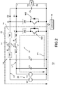
- FIG. 2 shows a block circuit diagram of a step-up conversion module with a protection circuit according to a first embodiment of the present disclosure.
- a step-up conversion module 10 is coupled between a solar cell module 20 and a load 30, and the step-up conversion module 10 converts the energy generated from the solar cell module 20 into an output power Vo for supplying power to the load 30.
- the step-up conversion module 10 includes a first step-up circuit 12, a second step-up circuit 14, a control unit 16, an output capacitor Co, and a protection circuit 18.
- Each of the first step-up circuit 12 and the second step-up circuit 14 forms a step-up converter respectively.
- the first step-up circuit 12 includes a first inductor L1, a first power diode D1, and a first switch unit 122
- the second step-up circuit 14 includes a second inductor L2, a second power diode D2, and a second switch unit 142.
- a first end of the first inductor L1 is coupled to one of solar cells in the solar cell module 20 to receive a first power VI
- a second end of the first inductor L1 is coupled to a first end of the first power diode D1 through a first node A.
- a first end of the first switch unit 122 is coupled to the first node A, and a second end of the first switch unit 122 is coupled to a negative end.
- a first end of the second inductor L2 is coupled to a second power V2, and a second end of the second inductor L2 is coupled to a first end of the second power diode D2 through a second node B.
- a first end of the second switch unit 142 is coupled to the second node B, and a second end of the second switch unit 142 is coupled to the negative end.
- the control unit 16 is coupled to the first switch unit 122, and controls the first step-up circuit 12 to convert the first power V1 into the output power Vo by switching the first switch unit 122. Also, the operation of the second step-up circuit 14 is similar.
- the output capacitor Co is coupled to a second end of the first power diode D1 and a second end of the second power diode D2, and stabilizes the output power Vo.
- the first inductor L1 and the second inductor L2 form a common-core coupling inductor Lc.
- two homonymous ends of the coupling inductor Lc are coupled to a positive end of the first power V1 and a positive end of the second power V2, respectively.
- Two sets or multiple sets of step-up circuits commonly use an inductor by the manner of coupling inductor Lc.
- the control unit 16 synchronously switches the first switch unit 122 and the second switch unit 142, that is, the first switch unit 122 and the second switch unit 142 are controlled to be turned on and turned off at the same time through a control signal with approximately the same duty cycle.
- the approximately the same duty cycle means an error of the duty cycle is within an error range, such as 10%, and therefore the error range allows that the control signals of controlling the first switch unit 122 and the second switch unit 142 have a slight phase shift or duty cycles of the two control signals are slightly different. Therefore, a voltage difference between the first power V1 and the second power V2 is within a first predetermined range so that a first current 11 flowing through the first inductor L1 is substantially equal to a second current 12 flowing through the second inductor L2.
- the inductance of the step-up circuit having the smaller input voltage induces a reverse current in the other direction due to the coupling effect.
- the reverse current will cause circulating current loss to reduce the efficiency of the step-up conversion module 10.
- the first step-up circuit 12 includes a first input loop Li1 composed of the first power VI, the first inductor L1, and the first switch unit 122.
- the first inductor L1 induces a first reverse current If1 (i.e., the reverse current is induced by the dotted end) due to the coupling effect. Since the step-up conversion module 10 does not have the protection circuit 18, there is no unidirectional conduction element on the first input loop Li1 to prevent the first reverse current If1.
- the first reverse current If1 flows through the first inductor L1, the first power V1 (or a first input capacitor CI), the first switch unit 122 to reduce the efficiency of the step-up conversion module 10.
- a second reverse current If2 generated by a second input loop Li2 of the second step-up circuit 14 is similar, which will not be repeated here.
- the protection circuit 18 includes a first unidirectional conduction element 182 and a second unidirectional conduction element 184.
- the first unidirectional conduction element 182 is coupled to the first input loop Li1 to block a first reverse current If1 induced by the coupling inductor Lc to the first inductor L1.
- the second unidirectional conduction element 184 is coupled to the second input loop Li2 to block a second reverse current If2 induced by the coupling inductor Lc to the second inductor L2.
- the first unidirectional conduction element 182 can be arranged in at least three positions in the first input loop Li1.
- the first position is that the first unidirectional conduction element 182 is coupled between the first inductor L1 and the first node A.
- the second position is that the first unidirectional conduction element 182 is coupled between the first node A and the first switch unit 122.
- the above-mentioned two coupling positions can be reversely biased to block the first reverse current If1 coupled to the first inductor L1 from the coupling inductor Lc.
- the third position is that the first unidirectional conduction element 182 is coupled between the first power V1 and the first inductor L1.
- the best coupling position of the first unidirectional conduction element 182 is the second position above. Since the first current I1 alternately operates between the first switch unit 122 and the output capacitor Co, the average current is smaller and this loss is also lower compared with the other two positions when the first unidirectional conduction element 182 is coupled between the first node A and the first switch unit 122.
- the coupling position of the second unidirectional conduction element 184 is similar, which will not be repeated here.
- the first unidirectional conduction element 182 and the second unidirectional conduction element 184 may be diodes, thyristors, or silicon-controlled rectifiers, or formed by unidirectional conduction circuits, such as but not limited to logic switch circuits. Since the diode does not need to be controlled and the circuit is simple, it is best to use diodes for the first unidirectional conduction element 182 and the second unidirectional conduction element 184.
- FIG. 3 shows a block circuit diagram of the step-up conversion module with the protection circuit according to a second embodiment of the present disclosure, and also refer to FIG. 2 .
- the major difference between the step-up conversion module 10' shown in FIG. 3 and the step-up conversion module 10 shown in FIG. 2 is that the first step-up circuit 12' and the second step-up circuit 14' of the former are flying-capacitor step-up converters.
- the first step-up circuit 12' includes a first inductor L1, a first switch unit 122', a first diode assembly 124, and a first flying capacitor 126, and the second step-up circuit 14' incudes a second inductor L2, a second switch unit 142', a second diode assembly 144, and a second flying capacitor 146.
- a first end of the first inductor L1 is coupled to the first power VI, and a second end of the first inductor L1 is coupled to a first end of the first diode assembly 124 through a first node A.
- a first end of the first switch unit 122' is coupled to the first node A, and a second end of the first switch unit 122' is coupled to a negative end.
- the first diode assembly 124 includes a first power diode D1 and a second power diode D2 connected in series, and the first power diode D1 is coupled to the first node A.
- the first switch unit 122' includes a first power switch Q1 and a second power switch Q2 connected in series, and the first power switch Q1 is coupled to the first node A and the second power switch Q2 is coupled to the negative end.
- a first end of the first flying capacitor 126 is coupled to the first power switch Q1 and the second power switch Q2, and a second end of the first flying capacitor 126 is coupled to the first power diode D1 and the second power diode D2.
- a first end of the second inductor L2 is coupled to the second power V2, and a second end of the second inductor L2 is coupled to a first end of the second diode assembly 144 through a second node B.
- a first end of the second switch unit 142' is coupled to the second node B, and a second end of the second switch unit 142' is coupled to the negative end.
- the second diode assembly 144 includes a third power diode D3 and a fourth power diode D4 connected in series, and the third power diode D3 is coupled to the second node B.
- the second switch unit 142' includes a third power switch Q3 and a fourth power switch Q4 connected in series, and the third power switch Q3 is coupled to the second node B and the fourth power switch Q4 is coupled to the negative end.
- a first end of the second flying capacitor 146 is coupled to the third power switch Q3 and the fourth power switch Q4, and a second end of the second flying capacitor 146 is coupled to the third power diode D3 and the fourth power diode D4.
- the control unit 16 is coupled to the first power switch Q1 and the second power switch Q2, and controls the first step-up circuit 12' to convert the first power V1 into the output power Vo by switching the first power switch Q1 and the second power switch Q2. Also, the operation of the second step-up circuit 14' is similar.
- the output capacitor Co is coupled to a second end of the second power diode D2 and a second end of the fourth power diode D4, and stabilizes the output power Vo.
- the manner of controlling the coupling inductor Lc with a common-core structure composed of the first inductor L1 and the second inductor L2 is similar to the FIG. 2 .
- the control unit 16 substantially synchronously switches the first switch unit 122' and the second switch unit 142', that is, the first power switch Q1 and the third power switch Q3 are substantially synchronous, and the second power switch Q2 and the fourth power switch Q4 are substantially synchronous.
- the first step-up circuit 12 includes a first input loop Li1 composed of a first power VI, a first inductor L1, and a first switch unit 122'.
- the first inductor L1 induces a first reverse current If1.
- a second reverse current If2 generated by the second input loop Li2 of the second step-up circuit 14' is similar, which will not be repeated here. Therefore, the protection circuit 18 blocks the first reverse current If1 through the first unidirectional conduction element 182 coupled to the first input loop Li1 and blocks the second reverse current If2 through the second unidirectional conduction element 184 coupled to the second input loop Li2.
- the first unidirectional conduction element 182 can be arranged in at least three positions in the first input loop Li1.
- the first position is that the first unidirectional conduction element 182 is coupled between the first inductor L1 and the first node A.
- the second position is that the first unidirectional conduction element 182 is coupled between the first node A and the first switch unit 122' (i.e., the first power switch Q1 of the first switch unit 122').
- the third position is that the first unidirectional conduction element 182 is coupled between the first power V1 and the first inductor L1.
- the three coupling positions can be reversely biased to block the first reverse current If1 coupled to the first inductor L1 from the coupling inductor Lc.
- step-up conversion module 10 shown in FIG. 2 and FIG. 3 has only two step-up circuits, it is not limited to this. In other words, the step-up conversion module 10 may have more than two step-up circuits, and the coupling inductor Lc is composed of common-core inductors of the step-up circuits.
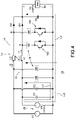
- FIG. 4 shows a block circuit diagram of the step-up conversion module with the protection circuit according to a third embodiment of the present disclosure, and also refer to FIG. 2 and FIG. 3 .
- the protection circuit 18 further includes a third unidirectional conduction element 186 and a fourth unidirectional conduction element 188.
- the third unidirectional conduction element 186 is connected to an input end of the first step-up circuit 12, i.e., connected to the first power V1 in parallel to provide a first reverse clamping path Lr1.
- the fourth unidirectional conduction element 188 is connected to an input end of the second step-up circuit 14, i.e., connected to the second power V2 in parallel to provide a second reverse clamping path Lr2.
- the protection circuit 18 When the protection circuit 18 has no the third unidirectional conduction element 186 and the fourth unidirectional conduction element 188, and one of the first step-up circuit 12 and the second step-up circuit 14 is reversely connected to the input power, the output power Vo is provided on the output capacitor Co since the step-up circuit correctly connected to the input power normally operates.
- the power diode of the step-up circuit reversely connected to the input power withstands a voltage of the input power plus the output power Vo, i.e., a voltage superimposed path Lv. If the power diode does not specifically select a high withstand voltage for this situation, the power diode will be damaged due to the overvoltage.
- the third unidirectional conduction element 186 and the fourth unidirectional conduction element 188 may be diodes, thyristors, or silicon-controlled rectifiers, or formed by unidirectional conduction circuits, such as but not limited to logic switch circuits. Since the diode does not need to be controlled and the circuit is simple, it is best to use diodes for the third unidirectional conduction element 186 and the fourth unidirectional conduction element 188.
- the second step-up circuit 14 outputs the second power V2 with 1000 volts to the output capacitor Co so that the voltage across the output capacitor Co is 1000 volts.
- the voltage on voltage superimposed path Lv is up to 2000 volts, and therefore the first power diode D1 must withstand 2000-volt voltage.
- the first power diode D1 withstands half the voltage of the output capacitor Co and the reversely-connected input power, but it will still be damaged.
- the third unidirectional conduction element 186 of the protection circuit 18 provides a first reverse clamping path Lr1. Once the first power V1 is reversely connected, the reversed first power V1 can be clamped to a low voltage through the first reverse clamping path Lr1 without superimposing its voltage on the first power diode D1. Therefore, the step-up conversion module 10 can continuously operate under the undamaged first power diode D1, and the first unidirectional conduction element 182 is used to block the first reverse current If1. The unidirectional conduction element 188 also provides this function, which will not be repeated here. In addition, the step-up conversion module 10' shown in FIG. 3 also applies the third unidirectional conduction element 186 and the fourth unidirectional conduction element 188 to protect the first power diode D1 and the third power diode D3, which will not be repeated here.
- FIG. 5 shows a block circuit diagram of the step-up conversion module with the protection circuit according to a fourth embodiment of the present disclosure, and also refer to FIG. 2 to FIG. 4 .
- the protection circuit 18 further includes a current measuring unit 190, and the current measuring unit 190 is coupled to a common-negative path Lg of the first input loop Li1 and the second input loop Li2 to sense a total current It flowing through the first step-up circuit 12 and the second step-up circuit 14.
- the current measuring unit 190 is coupled to a common-negative path Lg of the first input loop Li1 and the second input loop Li2 to sense a total current It flowing through the first step-up circuit 12 and the second step-up circuit 14.
- the first step-up circuit 12 and the second step-up circuit 14 are integrated into a single step-up conversion module 10.
- the second end of the first switch unit 122 and the second end of the second switch unit 142 are commonly coupled so that first input loop Li1 and the second input loop Li2 form a common-negative path Lg so that the total current It of the first step-up circuit 12 and the second step-up circuit 14 can be measured by using only one current measuring unit 190.
- the control unit 16 controls a first current I1 flowing through the first inductor L1 is substantially equal to a second current 12 flowing through the second inductor L2, and therefore the total current It measured by the current measuring unit 190 is substantially equal to an average current of the first current I1 and the second current 12.
- FIG. 6 shows a block circuit diagram of the step-up conversion module with the protection circuit according to a fifth embodiment of the present disclosure, and also refer to FIG. 2 to FIG. 5 .
- the step-up conversion module 10 further includes a current transforming unit 192.
- the current transforming unit 192 is coupled to the coupling inductor Lc.
- the current transforming unit 192 may be coupled between the coupling inductor Lc and the first power V1 and the second power V2.
- the current transforming unit 192 may be coupled between the coupling inductor Lc and the first node A and the second node B.
- the current transforming unit 192 is similar to the coupling inductor Lc, which is wound by coils, the connection relationship between the dotted end and the first power V1 and the second power V2 is different from that of the coupling inductor Lc, and the number of coils is also small. As shown in FIG. 6 , two heteronymous ends of the current transforming unit 192 are coupled to two homonymous ends of the coupling inductor Lc. When a voltage difference between the first power V1 and the second power V2 is within a second predetermined range, the current transforming unit 192 maintains the first current I1 flowing through the first inductor L1 to be equal to the second current 12 flowing through the second inductor L2.
- the current transforming unit 192 induces to the second step-up circuit 14 through the coupling effect to reduce the current difference between the first current I1 and the second current 12 so as to maintain the first current I1 to be equal to the second current 12, and vice versa. Therefore, the second predetermined range is greater than the first predetermined range, that is, when the voltage difference between the first power V1 and the second power V2 is greater, the step-up conversion module 10 using the current transforming unit 192 can still maintain the first current I1 to be equal to the second current 12.
Landscapes
- Engineering & Computer Science (AREA)
- Power Engineering (AREA)
- Dc-Dc Converters (AREA)
Abstract
Description
- The present disclosure relates to a step-up conversion module with a protection circuit, and more particularly to a step-up conversion module with a protection circuit having a common-core structure.
- The statements in this section merely provide background information related to the present disclosure and do not necessarily constitute prior art.
- Please refer to
FIG. 1 , which shows a circuit diagram of a conventional step-up conversion module applied to a solar cell module. In this structure, there are two independent step-up circuits 10-2,10-3. The two step-up circuits 10-2,10-3 convert a first power V1 and a second power V2 into an output power Vo, respectively. Since thesolar cell module 20 includes multiple sets of solar cells, each set of solar cells must use a step-up circuit to convert its electrical energy into the output power Vo. Therefore, when thesolar cell module 20 is installed in a large area, the step-up conversion module 10-1 must include multiple sets of step-up circuits, which cause the circuit area of the step-up conversion module 10-1 to be too large and to be conducive to the installation of the step-up conversion module 10-1. The bulky component in the step-up circuit is usually the internal inductor L with an iron core and coils, and the size of the iron core is the main cause of the excessive volume of the internal inductor L, and therefore the size of the step-up conversion module 10-1 is difficult to be reduced. - Further, since the step-up conversion module 10-1 is composed of multiple sets of step-up circuits in parallel, when the
solar cell module 20 has a problem, for example but not limited to reversely connected or no output due to damage, it often not only affects the corresponding coupled step-up circuit but also affects step-up circuits of other step-up conversion modules through the parallel structure to cause problems of the operations of the step-up circuits, thereby reducing the efficiency of the step-up conversion module 10-1. - Accordingly, how to design a step-up conversion module with a protection circuit to use a common-core circuit component to reduce the volume of the step-up conversion module and to provide the protection circuit to avoid that the step-up circuits in the step-up conversion module do not affect to each other when the solar cell module is in trouble is a major subject for the inventors of the present disclosure.
- In order to solve the above-mentioned problems, the present disclosure provides a step-up conversion module with a protection circuit. The step-up conversion module includes a first step-up circuit, a second step-up circuit, a first unidirectional conduction element, and a second unidirectional conduction element. The first step-up circuit is coupled to a first power, and has a first input loop composed of a first inductor and a first switch unit. The second step-up circuit is coupled to a second power, and has a second input loop composed of a second inductor and a second switch unit. The first inductor and the second inductor form a coupling inductor with a common core. The first unidirectional conduction element is coupled to the first input loop, and blocks a first reverse current induced by the coupling inductor to the first input loop. The second unidirectional conduction element is coupled to the second input loop, and blocks a second reverse current induced by the coupling inductor to the second input loop.
- The main purpose and effect of the present disclosure is to use the coupling inductor with a common-core structure to reduce the volume of the step-up conversion module, and use the protection circuit to avoid that when the voltage of one of the solar cells is very low, it corresponding step-up circuit does not generate reverse current, thereby increasing the operation efficiency of the step-up conversion module.
- It is to be understood that both the foregoing general description and the following detailed description are exemplary, and are intended to provide further explanation of the present disclosure as claimed. Other advantages and features of the present disclosure will be apparent from the following description, drawings, and claims.
- The present disclosure can be more fully understood by reading the following detailed description of the embodiment, with reference made to the accompanying drawings as follows:
-
FIG. 1 is a circuit diagram of a conventional step-up conversion module applied to a solar cell module. -
FIG. 2 is a block circuit diagram of a step-up conversion module with a protection circuit according to a first embodiment of the present disclosure. -
FIG. 3 is a block circuit diagram of the step-up conversion module with the protection circuit according to a second embodiment of the present disclosure. -
FIG. 4 is a block circuit diagram of the step-up conversion module with the protection circuit according to a third embodiment of the present disclosure. -
FIG. 5 is a block circuit diagram of the step-up conversion module with the protection circuit according to a fourth embodiment of the present disclosure. -
FIG. 6 is a block circuit diagram of the step-up conversion module with the protection circuit according to a fifth embodiment of the present disclosure. - Reference will now be made to the drawing figures to describe the present disclosure in detail. It will be understood that the drawing figures and exemplified embodiments of present disclosure are not limited to the details thereof.
- Please refer to
FIG. 2 , which shows a block circuit diagram of a step-up conversion module with a protection circuit according to a first embodiment of the present disclosure. A step-up conversion module 10 is coupled between asolar cell module 20 and aload 30, and the step-up conversion module 10 converts the energy generated from thesolar cell module 20 into an output power Vo for supplying power to theload 30. The step-up conversion module 10 includes a first step-up circuit 12, a second step-up circuit 14, acontrol unit 16, an output capacitor Co, and aprotection circuit 18. Each of the first step-upcircuit 12 and the second step-upcircuit 14 forms a step-up converter respectively. The first step-up circuit 12 includes a first inductor L1, a first power diode D1, and afirst switch unit 122, and the second step-up circuit 14 includes a second inductor L2, a second power diode D2, and asecond switch unit 142. A first end of the first inductor L1 is coupled to one of solar cells in thesolar cell module 20 to receive a first power VI, and a second end of the first inductor L1 is coupled to a first end of the first power diode D1 through a first node A. A first end of thefirst switch unit 122 is coupled to the first node A, and a second end of thefirst switch unit 122 is coupled to a negative end. A first end of the second inductor L2 is coupled to a second power V2, and a second end of the second inductor L2 is coupled to a first end of the second power diode D2 through a second node B. A first end of thesecond switch unit 142 is coupled to the second node B, and a second end of thesecond switch unit 142 is coupled to the negative end. Thecontrol unit 16 is coupled to thefirst switch unit 122, and controls the first step-up circuit 12 to convert the first power V1 into the output power Vo by switching thefirst switch unit 122. Also, the operation of the second step-upcircuit 14 is similar. The output capacitor Co is coupled to a second end of the first power diode D1 and a second end of the second power diode D2, and stabilizes the output power Vo. - In order to integrate the first inductor L1 and the second inductor L2 into one to reduce the volume of the step-
up conversion module 10 and decrease the circuit cost, the first inductor L1 and the second inductor L2 form a common-core coupling inductor Lc. As shown inFIG. 2 , two homonymous ends of the coupling inductor Lc are coupled to a positive end of the first power V1 and a positive end of the second power V2, respectively. Two sets or multiple sets of step-up circuits commonly use an inductor by the manner of coupling inductor Lc. Thecontrol unit 16 synchronously switches thefirst switch unit 122 and thesecond switch unit 142, that is, thefirst switch unit 122 and thesecond switch unit 142 are controlled to be turned on and turned off at the same time through a control signal with approximately the same duty cycle. The approximately the same duty cycle means an error of the duty cycle is within an error range, such as 10%, and therefore the error range allows that the control signals of controlling thefirst switch unit 122 and thesecond switch unit 142 have a slight phase shift or duty cycles of the two control signals are slightly different. Therefore, a voltage difference between the first power V1 and the second power V2 is within a first predetermined range so that afirst current 11 flowing through the first inductor L1 is substantially equal to asecond current 12 flowing through the second inductor L2. Once the voltage difference between the first power V1 and the second power V2 is excessive, however, the inductance of the step-up circuit having the smaller input voltage induces a reverse current in the other direction due to the coupling effect. The reverse current will cause circulating current loss to reduce the efficiency of the step-upconversion module 10. - Specifically, the first step-
up circuit 12 includes a first input loop Li1 composed of the first power VI, the first inductor L1, and thefirst switch unit 122. When the voltage of the first power V1 is much smaller than the voltage of the second power V2 to cause thesecond current 12 flowing through the second inductor L2, the first inductor L1 induces a first reverse current If1 (i.e., the reverse current is induced by the dotted end) due to the coupling effect. Since the step-upconversion module 10 does not have theprotection circuit 18, there is no unidirectional conduction element on the first input loop Li1 to prevent the first reverse current If1. At this condition, the first reverse current If1 flows through the first inductor L1, the first power V1 (or a first input capacitor CI), thefirst switch unit 122 to reduce the efficiency of the step-up conversion module 10. In addition, a second reverse current If2 generated by a second input loop Li2 of the second step-upcircuit 14 is similar, which will not be repeated here. - For example, under the absence of the
protection circuit 18, it is assumed that the first power V1 is 200 volts and the second power V2 is close to 0 volt, that is, the second step-upcircuit 14 may not be coupled to the solar cell or the corresponding solar cell may be shaded. At this condition, since the voltage of the second power V2 is much smaller than the voltage of the first power VI, the second inductor L2 generates an induced voltage due to the coupling effect of the coupling inductor Lc, thereby generating the second reverse current If2. In order to avoid this situation, theprotection circuit 18 includes a firstunidirectional conduction element 182 and a secondunidirectional conduction element 184. The firstunidirectional conduction element 182 is coupled to the first input loop Li1 to block a first reverse current If1 induced by the coupling inductor Lc to the first inductor L1. The secondunidirectional conduction element 184 is coupled to the second input loop Li2 to block a second reverse current If2 induced by the coupling inductor Lc to the second inductor L2. - The first
unidirectional conduction element 182 can be arranged in at least three positions in the first input loop Li1. The first position is that the firstunidirectional conduction element 182 is coupled between the first inductor L1 and the first node A. The second position is that the firstunidirectional conduction element 182 is coupled between the first node A and thefirst switch unit 122. The above-mentioned two coupling positions can be reversely biased to block the first reverse current If1 coupled to the first inductor L1 from the coupling inductor Lc. The third position is that the firstunidirectional conduction element 182 is coupled between the first power V1 and the first inductor L1. However, it is not limited to only the above-mentioned three positions, as long as it is positioned in the first input loop Li1 to block the first reverse current If1. The specific coupling positions of the secondunidirectional conduction element 184 is also similar, and will not be repeated here. - The best coupling position of the first
unidirectional conduction element 182 is the second position above. Since the first current I1 alternately operates between thefirst switch unit 122 and the output capacitor Co, the average current is smaller and this loss is also lower compared with the other two positions when the firstunidirectional conduction element 182 is coupled between the first node A and thefirst switch unit 122. The coupling position of the secondunidirectional conduction element 184 is similar, which will not be repeated here. In particular, the firstunidirectional conduction element 182 and the secondunidirectional conduction element 184 may be diodes, thyristors, or silicon-controlled rectifiers, or formed by unidirectional conduction circuits, such as but not limited to logic switch circuits. Since the diode does not need to be controlled and the circuit is simple, it is best to use diodes for the firstunidirectional conduction element 182 and the secondunidirectional conduction element 184. - Please refer to
FIG. 3 , which shows a block circuit diagram of the step-up conversion module with the protection circuit according to a second embodiment of the present disclosure, and also refer toFIG. 2 . The major difference between the step-up conversion module 10' shown inFIG. 3 and the step-upconversion module 10 shown inFIG. 2 is that the first step-up circuit 12' and the second step-up circuit 14' of the former are flying-capacitor step-up converters. The first step-up circuit 12' includes a first inductor L1, a first switch unit 122', afirst diode assembly 124, and afirst flying capacitor 126, and the second step-up circuit 14' incudes a second inductor L2, a second switch unit 142', asecond diode assembly 144, and asecond flying capacitor 146. A first end of the first inductor L1 is coupled to the first power VI, and a second end of the first inductor L1 is coupled to a first end of thefirst diode assembly 124 through a first node A. A first end of the first switch unit 122' is coupled to the first node A, and a second end of the first switch unit 122' is coupled to a negative end. Thefirst diode assembly 124 includes a first power diode D1 and a second power diode D2 connected in series, and the first power diode D1 is coupled to the first node A. The first switch unit 122' includes a first power switch Q1 and a second power switch Q2 connected in series, and the first power switch Q1 is coupled to the first node A and the second power switch Q2 is coupled to the negative end. A first end of the first flyingcapacitor 126 is coupled to the first power switch Q1 and the second power switch Q2, and a second end of the first flyingcapacitor 126 is coupled to the first power diode D1 and the second power diode D2. - A first end of the second inductor L2 is coupled to the second power V2, and a second end of the second inductor L2 is coupled to a first end of the
second diode assembly 144 through a second node B. A first end of the second switch unit 142' is coupled to the second node B, and a second end of the second switch unit 142' is coupled to the negative end. Thesecond diode assembly 144 includes a third power diode D3 and a fourth power diode D4 connected in series, and the third power diode D3 is coupled to the second node B. The second switch unit 142' includes a third power switch Q3 and a fourth power switch Q4 connected in series, and the third power switch Q3 is coupled to the second node B and the fourth power switch Q4 is coupled to the negative end. A first end of thesecond flying capacitor 146 is coupled to the third power switch Q3 and the fourth power switch Q4, and a second end of thesecond flying capacitor 146 is coupled to the third power diode D3 and the fourth power diode D4. - The
control unit 16 is coupled to the first power switch Q1 and the second power switch Q2, and controls the first step-up circuit 12' to convert the first power V1 into the output power Vo by switching the first power switch Q1 and the second power switch Q2. Also, the operation of the second step-up circuit 14' is similar. The output capacitor Co is coupled to a second end of the second power diode D2 and a second end of the fourth power diode D4, and stabilizes the output power Vo. The manner of controlling the coupling inductor Lc with a common-core structure composed of the first inductor L1 and the second inductor L2 is similar to theFIG. 2 . Thecontrol unit 16 substantially synchronously switches the first switch unit 122' and the second switch unit 142', that is, the first power switch Q1 and the third power switch Q3 are substantially synchronous, and the second power switch Q2 and the fourth power switch Q4 are substantially synchronous. - The first step-up
circuit 12 includes a first input loop Li1 composed of a first power VI, a first inductor L1, and a first switch unit 122'. When the voltage of the first power V1 is much smaller than the voltage of the second power V2 to cause the second current 12 flowing through the second inductor L2, the first inductor L1 induces a first reverse current If1. In addition, a second reverse current If2 generated by the second input loop Li2 of the second step-up circuit 14' is similar, which will not be repeated here. Therefore, theprotection circuit 18 blocks the first reverse current If1 through the firstunidirectional conduction element 182 coupled to the first input loop Li1 and blocks the second reverse current If2 through the secondunidirectional conduction element 184 coupled to the second input loop Li2. - It is similar to
FIG. 2 , the firstunidirectional conduction element 182 can be arranged in at least three positions in the first input loop Li1. The first position is that the firstunidirectional conduction element 182 is coupled between the first inductor L1 and the first node A. The second position is that the firstunidirectional conduction element 182 is coupled between the first node A and the first switch unit 122' (i.e., the first power switch Q1 of the first switch unit 122'). The third position is that the firstunidirectional conduction element 182 is coupled between the first power V1 and the first inductor L1. The three coupling positions can be reversely biased to block the first reverse current If1 coupled to the first inductor L1 from the coupling inductor Lc. The specific coupling positions of the secondunidirectional conduction element 184 is also similar, and will not be repeated here. Although the step-upconversion module 10 shown inFIG. 2 andFIG. 3 has only two step-up circuits, it is not limited to this. In other words, the step-upconversion module 10 may have more than two step-up circuits, and the coupling inductor Lc is composed of common-core inductors of the step-up circuits. - Please refer to
FIG. 4 , which shows a block circuit diagram of the step-up conversion module with the protection circuit according to a third embodiment of the present disclosure, and also refer toFIG. 2 andFIG. 3 . Take the step-upconversion module 10 shown inFIG. 2 as an example, theprotection circuit 18 further includes a thirdunidirectional conduction element 186 and a fourthunidirectional conduction element 188. The thirdunidirectional conduction element 186 is connected to an input end of the first step-upcircuit 12, i.e., connected to the first power V1 in parallel to provide a first reverse clamping path Lr1. The fourthunidirectional conduction element 188 is connected to an input end of the second step-upcircuit 14, i.e., connected to the second power V2 in parallel to provide a second reverse clamping path Lr2. - When the
protection circuit 18 has no the thirdunidirectional conduction element 186 and the fourthunidirectional conduction element 188, and one of the first step-upcircuit 12 and the second step-upcircuit 14 is reversely connected to the input power, the output power Vo is provided on the output capacitor Co since the step-up circuit correctly connected to the input power normally operates. At this condition, the power diode of the step-up circuit reversely connected to the input power withstands a voltage of the input power plus the output power Vo, i.e., a voltage superimposed path Lv. If the power diode does not specifically select a high withstand voltage for this situation, the power diode will be damaged due to the overvoltage. In particular, the thirdunidirectional conduction element 186 and the fourthunidirectional conduction element 188 may be diodes, thyristors, or silicon-controlled rectifiers, or formed by unidirectional conduction circuits, such as but not limited to logic switch circuits. Since the diode does not need to be controlled and the circuit is simple, it is best to use diodes for the thirdunidirectional conduction element 186 and the fourthunidirectional conduction element 188. - Take the
FIG. 4 as an example, it is assumed that the first power V1 is 1000 volts and reversely connected, the second step-upcircuit 14 outputs the second power V2 with 1000 volts to the output capacitor Co so that the voltage across the output capacitor Co is 1000 volts. At this condition, the voltage on voltage superimposed path Lv is up to 2000 volts, and therefore the first power diode D1 must withstand 2000-volt voltage. The same situation also occurs to the first power diode D1 shown inFIG. 3 . However, the first power diode D1 withstands half the voltage of the output capacitor Co and the reversely-connected input power, but it will still be damaged. In order to avoid this situation, the thirdunidirectional conduction element 186 of theprotection circuit 18 provides a first reverse clamping path Lr1. Once the first power V1 is reversely connected, the reversed first power V1 can be clamped to a low voltage through the first reverse clamping path Lr1 without superimposing its voltage on the first power diode D1. Therefore, the step-upconversion module 10 can continuously operate under the undamaged first power diode D1, and the firstunidirectional conduction element 182 is used to block the first reverse current If1. Theunidirectional conduction element 188 also provides this function, which will not be repeated here. In addition, the step-up conversion module 10' shown inFIG. 3 also applies the thirdunidirectional conduction element 186 and the fourthunidirectional conduction element 188 to protect the first power diode D1 and the third power diode D3, which will not be repeated here. - Please refer to
FIG. 5 , which shows a block circuit diagram of the step-up conversion module with the protection circuit according to a fourth embodiment of the present disclosure, and also refer toFIG. 2 to FIG. 4 . Take the step-upconversion module 10 shown inFIG. 2 as an example, theprotection circuit 18 further includes acurrent measuring unit 190, and thecurrent measuring unit 190 is coupled to a common-negative path Lg of the first input loop Li1 and the second input loop Li2 to sense a total current It flowing through the first step-upcircuit 12 and the second step-upcircuit 14. In the prior art, when two step-up converters measure currents, each of the two step-up converter measure currents needs to use a current measuring unit to respectively measure the currents. Even if the two step-up converters are controlled in a current-shared condition, they still need to use a current measuring unit to measure their respective currents. In the present disclosure, the first step-upcircuit 12 and the second step-upcircuit 14 are integrated into a single step-upconversion module 10. The second end of thefirst switch unit 122 and the second end of thesecond switch unit 142 are commonly coupled so that first input loop Li1 and the second input loop Li2 form a common-negative path Lg so that the total current It of the first step-upcircuit 12 and the second step-upcircuit 14 can be measured by using only onecurrent measuring unit 190. When a voltage difference between the first power V1 and the second power V2 is within a first predetermined range, thecontrol unit 16 controls a first current I1 flowing through the first inductor L1 is substantially equal to a second current 12 flowing through the second inductor L2, and therefore the total current It measured by thecurrent measuring unit 190 is substantially equal to an average current of the first current I1 and the second current 12. - Please refer to
FIG. 6 , which shows a block circuit diagram of the step-up conversion module with the protection circuit according to a fifth embodiment of the present disclosure, and also refer toFIG. 2 to FIG. 5 . Take the step-upconversion module 10 shown inFIG. 2 as an example, the step-upconversion module 10 further includes a current transformingunit 192. The current transformingunit 192 is coupled to the coupling inductor Lc. Specifically, the current transformingunit 192 may be coupled between the coupling inductor Lc and the first power V1 and the second power V2. Alternatively, the current transformingunit 192 may be coupled between the coupling inductor Lc and the first node A and the second node B. Although the current transformingunit 192 is similar to the coupling inductor Lc, which is wound by coils, the connection relationship between the dotted end and the first power V1 and the second power V2 is different from that of the coupling inductor Lc, and the number of coils is also small. As shown inFIG. 6 , two heteronymous ends of the current transformingunit 192 are coupled to two homonymous ends of the coupling inductor Lc. When a voltage difference between the first power V1 and the second power V2 is within a second predetermined range, the current transformingunit 192 maintains the first current I1 flowing through the first inductor L1 to be equal to the second current 12 flowing through the second inductor L2. - The reason is that two dotted ends of the two windings of the current transforming
unit 192 are opposite. Therefore, when the first current I1 is larger, the current transformingunit 192 induces to the second step-upcircuit 14 through the coupling effect to reduce the current difference between the first current I1 and the second current 12 so as to maintain the first current I1 to be equal to the second current 12, and vice versa. Therefore, the second predetermined range is greater than the first predetermined range, that is, when the voltage difference between the first power V1 and the second power V2 is greater, the step-upconversion module 10 using the current transformingunit 192 can still maintain the first current I1 to be equal to the second current 12.
Claims (14)
- A step-up conversion module with a protection circuit (18), characterized in that the step-up conversion module (10,10') comprising:a first step-up circuit (12,12') coupled to a first power (V1), and having a first input loop (Li1) composed of a first inductor (LI) and a first switch unit (122,122'),a second step-up circuit (14,14') coupled to a second power (V2), and having a second input loop (Li2) composed of a second inductor (L2) and a second switch unit (142,142'), wherein the first inductor (LI) and the second inductor (L2) form a coupling inductor (Lc) with a common core,a first unidirectional conduction element (182) coupled to the first input loop (Li1), and configured to block a first reverse current (If1) induced by the coupling inductor (Lc) to the first input loop (Li1), anda second unidirectional conduction element (184) coupled to the second input loop (Li2), and configured to block a second reverse current (If2) induced by the coupling inductor (Lc) to the second input loop (Li2).
- The step-up conversion module (10,10') as claimed in claim 1, further comprising:a third unidirectional conduction element (186) connected to an input end of the first step-up circuit (12,12'), and configured to provide a first reverse clamping path (Lr1) when the first power (VI) is reversely connected, anda fourth unidirectional conduction element (188) connected to an input end of the second step-up circuit (14,14'), and configured to provide a second reverse clamping path (Lr2) when the second power (V2) is reversely connected.
- The step-up conversion module (10,10') as claimed in claim 2, wherein the first unidirectional conduction element (182), the second unidirectional conduction element (184), the third unidirectional conduction element (186), and the fourth unidirectional conduction element (188) are diodes.
- The step-up conversion module (10,10') as claimed in claim 1, wherein a first end of the first switch unit (122,122') is coupled to the first inductor (LI), a first end of the second switch unit (142,142') is coupled to the second inductor (L2), and a second end of the first switch unit (122,122') and a second end of the second switch unit (142,142') are commonly connected so that the first input loop (Li1) and the second input loop (Li2) form a common-negative path (Lg).
- The step-up conversion module (10,10') as claimed in claim 4, further comprising:a current measuring unit (190) coupled to the common-negative path (Lg), and configured to sense a total current (It) flowing through the first step-up circuit (12,12') and the second step-up circuit (14,14').
- The step-up conversion module (10,10') as claimed in claim 1, wherein two homonymous ends of the coupling inductor (Lc) are coupled to a positive end of the first power (VI) and a positive end of the second power (V2), respectively.
- The step-up conversion module (10,10') as claimed in claim 6, further comprising:a current transforming unit (192) coupled to the coupling inductor (Lc),wherein two heteronymous ends of the current transforming unit (192) are coupled to the two homonymous ends of the coupling inductor (Lc).
- The step-up conversion module (10,10') as claimed in claim 1, wherein each of the first step-up circuit (12,12') and the second step-up circuit (14,14') forms a step-up converter respectively; a first node (A) coupled to a first power diode (D1) is provided between the first inductor (LI) and the first switch unit (122,122'), and a second node (B) coupled to a second power diode (D2) is provided between the second inductor (L2) and the second switch unit (142,142').
- The step-up conversion module (10,10') as claimed in claim 8, wherein the first unidirectional conduction element (182) is coupled between the first inductor (LI) and the first node (A), or the first unidirectional conduction element (182) is coupled between the first node (A) and the first switch unit (122,122'), or the first unidirectional conduction element (182) is coupled between the first power (VI) and the first inductor (LI).
- The step-up conversion module (10,10') as claimed in claim 8, wherein the second unidirectional conduction element (184) is coupled between the second inductor (L2) and the second node (B), or the second unidirectional conduction element (184) is coupled between the second node (B) and the second switch unit (142,142'), or the second unidirectional conduction element (184) is coupled between the second power (V2) and the second inductor (L2).
- The step-up conversion module (10,10') as claimed in claim 1, wherein each of the first step-up circuit (12,12') and the second step-up circuit (14,14') forms a flying-capacitor step-up converter respectively; a first node (A) coupled to a first power diode assembly is provided between the first inductor (LI) and the first switch unit (122,122'), and a second node (B) coupled to a second power diode assembly is provided between the second inductor (L2) and the second switch unit (142,142').
- The step-up conversion module (10,10') as claimed in claim 11, wherein the first unidirectional conduction element (182) is coupled between the first inductor (LI) and the first node (A), or the first unidirectional conduction element (182) is coupled between the first node (A) and the first switch unit (122,122'), or the first unidirectional conduction element (182) is coupled between the first power (VI) and the first inductor (LI).
- The step-up conversion module (10,10') as claimed in claim 11, wherein the second unidirectional conduction element (184) is coupled between the second inductor (L2) and the second node (B), or the second unidirectional conduction element (184) is coupled between the second node (B) and the second switch unit (142,142'), or the second unidirectional conduction element (184) is coupled between the second power (V2) and the second inductor (L2).
- The step-up conversion module (10,10') as claimed in claim 1, wherein the first switch unit (122,122') and the second switch unit (142,142') are controlled to synchronously switch within an error range.
Applications Claiming Priority (1)
| Application Number | Priority Date | Filing Date | Title |
|---|---|---|---|
| CN202011090585.2A CN114362525A (en) | 2020-10-13 | 2020-10-13 | Boost conversion module with protection circuit |
Publications (1)
| Publication Number | Publication Date |
|---|---|
| EP3985852A1 true EP3985852A1 (en) | 2022-04-20 |
Family
ID=76829295
Family Applications (1)
| Application Number | Title | Priority Date | Filing Date |
|---|---|---|---|
| EP21183917.0A Pending EP3985852A1 (en) | 2020-10-13 | 2021-07-06 | Step-up conversion module with protection circuit |
Country Status (4)
| Country | Link |
|---|---|
| US (1) | US20220115983A1 (en) |
| EP (1) | EP3985852A1 (en) |
| JP (1) | JP7203911B2 (en) |
| CN (1) | CN114362525A (en) |
Families Citing this family (2)
| Publication number | Priority date | Publication date | Assignee | Title |
|---|---|---|---|---|
| CN115940637A (en) * | 2022-11-02 | 2023-04-07 | Oppo广东移动通信有限公司 | Power supply device, system, method, electronic device and readable storage medium |
| CN117595649B (en) * | 2023-11-27 | 2024-07-30 | 深圳市迪威电气有限公司 | Multiport input non-isolated direct current converter and control method thereof |
Citations (1)
| Publication number | Priority date | Publication date | Assignee | Title |
|---|---|---|---|---|
| US20120043923A1 (en) * | 2010-08-18 | 2012-02-23 | Alexandr Ikriannikov | System, Method, Module, And Energy Exchanger For Optimizing Output Of Series-Connected Photovoltaic And Electrochemical Devices |
Family Cites Families (17)
| Publication number | Priority date | Publication date | Assignee | Title |
|---|---|---|---|---|
| JP3405674B2 (en) * | 1998-01-28 | 2003-05-12 | デンセイ・ラムダ株式会社 | Forward converter for selecting and supplying different types of power |
| DE19803554A1 (en) * | 1998-01-30 | 1999-08-05 | Grohe Armaturen Friedrich | Water outlet fitting |
| US6084790A (en) * | 1999-01-07 | 2000-07-04 | Astec International Limited | Circuit to ensure equal current sharing and switching losses between parallel power devices |
| JP2001008440A (en) | 1999-06-17 | 2001-01-12 | Sony Corp | Power source circuit |
| JP4274485B2 (en) | 2006-03-16 | 2009-06-10 | 元智大学 | Self-efficiency single-stage multi-input bidirectional converter |
| JP4714250B2 (en) | 2008-09-10 | 2011-06-29 | 株式会社日立製作所 | DC-DC converter |
| JP4764499B2 (en) | 2009-08-05 | 2011-09-07 | 本田技研工業株式会社 | DC / DC converter and power supply system including the DC / DC converter |
| JP2013034279A (en) | 2011-08-01 | 2013-02-14 | Toyota Central R&D Labs Inc | Multi-phase converter circuit |
| CN103312153B (en) * | 2012-03-12 | 2016-04-27 | 南京航空航天大学 | A kind of parallel multi input coupling inductance buck-boost converter |
| WO2014192084A1 (en) * | 2013-05-28 | 2014-12-04 | 三菱電機株式会社 | Power convertor, motor drive control device equipped with power convertor, compressor and blower equipped with motor drive control device, and air conditioner equipped with compressor or blower |
| EP3736956A1 (en) * | 2014-04-16 | 2020-11-11 | Apple Inc. | Drive scheme for weakly coupled coils |
| TWI520472B (en) * | 2014-04-29 | 2016-02-01 | Univ Hungkuang | High efficiency wide range of output voltage of the DC power boost circuit |
| JP6064968B2 (en) * | 2014-10-10 | 2017-01-25 | トヨタ自動車株式会社 | Power system |
| JP6613951B2 (en) | 2016-02-22 | 2019-12-04 | 富士電機株式会社 | Power converter |
| JP6518604B2 (en) | 2016-02-24 | 2019-05-22 | 本田技研工業株式会社 | POWER SUPPLY DEVICE, DEVICE, AND CONTROL METHOD |
| WO2019145016A1 (en) * | 2018-01-23 | 2019-08-01 | Huawei Technologies Co., Ltd. | Power converter |
| EP3806309A4 (en) * | 2018-05-29 | 2021-06-02 | Mitsubishi Electric Corporation | Power conversion device |
-
2020
- 2020-10-13 CN CN202011090585.2A patent/CN114362525A/en active Pending
-
2021
- 2021-07-05 JP JP2021111510A patent/JP7203911B2/en active Active
- 2021-07-06 EP EP21183917.0A patent/EP3985852A1/en active Pending
- 2021-07-14 US US17/375,240 patent/US20220115983A1/en not_active Abandoned
Patent Citations (1)
| Publication number | Priority date | Publication date | Assignee | Title |
|---|---|---|---|---|
| US20120043923A1 (en) * | 2010-08-18 | 2012-02-23 | Alexandr Ikriannikov | System, Method, Module, And Energy Exchanger For Optimizing Output Of Series-Connected Photovoltaic And Electrochemical Devices |
Non-Patent Citations (6)
| Title |
|---|
| H. MATSUO ET AL: "Characteristics of the Multiple-Input DC-DC Converter", IEEE TRANSACTIONS ON INDUSTRIAL ELECTRONICS, vol. 51, no. 3, 14 January 2004 (2004-01-14), pages 625 - 631, XP055020225, ISSN: 0278-0046, DOI: 10.1109/TIE.2004.825362 * |
| HAMIDREZA KEYHANI ET AL: "Flying-capacitor boost converter", APPLIED POWER ELECTRONICS CONFERENCE AND EXPOSITION (APEC), 2012 TWENTY-SEVENTH ANNUAL IEEE, IEEE, 5 February 2012 (2012-02-05), pages 2311 - 2318, XP032127989, ISBN: 978-1-4577-1215-9, DOI: 10.1109/APEC.2012.6166145 * |
| KASPARS KROICS ET AL: "Multiphase interleaved DC-DC converter with directly and inversely coupled inductors", 2016 57TH INTERNATIONAL SCIENTIFIC CONFERENCE ON POWER AND ELECTRICAL ENGINEERING OF RIGA TECHNICAL UNIVERSITY (RTUCON), 1 October 2016 (2016-10-01), pages 1 - 6, XP055573219, ISBN: 978-1-5090-3731-5, DOI: 10.1109/RTUCON.2016.7763102 * |
| MOHANA KISHORE PINJALA ET AL: "Dual-input and triple-output boost hybrid converter suitable for grid-connected renewable energy sources", IET POWER ELECTRONICS, IET, UK, vol. 13, no. 4, 18 March 2020 (2020-03-18), pages 808 - 820, XP006089300, ISSN: 1755-4535, DOI: 10.1049/IET-PEL.2018.6398 * |
| SHEPARD PAUL: "Digitally-Controlled Three-Channel Interleaved PFC Reference Design", 12 October 2017 (2017-10-12), pages 1 - 2, XP055868610, Retrieved from the Internet <URL:https://eepower.com/news/three-channel-digitally-controlled-interleaved-pfc-reference-design/#> [retrieved on 20211202] * |
| YAOW-MING CHEN ET AL: "Multi-Input DC/DC Converter Based on the Multiwinding Transformer for Renewable Energy Applications", IEEE TRANSACTIONS ON INDUSTRY APPLICATIONS, IEEE SERVICE CENTER, PISCATAWAY, NJ, US, vol. 38, no. 4, 1 July 2002 (2002-07-01), XP011073486, ISSN: 0093-9994 * |
Also Published As
| Publication number | Publication date |
|---|---|
| US20220115983A1 (en) | 2022-04-14 |
| JP7203911B2 (en) | 2023-01-13 |
| JP2022064281A (en) | 2022-04-25 |
| CN114362525A (en) | 2022-04-15 |
Similar Documents
| Publication | Publication Date | Title |
|---|---|---|
| JP6302095B2 (en) | Switching power supply and method for controlling the switching power supply | |
| EP3934083B1 (en) | Isolated multi-phase dc/dc converter with reduced quantity of blocking capacitors | |
| EP0284172A2 (en) | Source volt-ampere/load volt-ampere differential converter | |
| US9787201B2 (en) | Bidirectional isolated multi-level DC-DC converter and method thereof | |
| US20220115983A1 (en) | Step-up conversion module with protection circuit | |
| US8885366B2 (en) | DC-to-DC voltage regulator and its operating method thereof | |
| CN103887974A (en) | Power supply | |
| Zhu et al. | Integrated Magnetic Buck–Boost Converter With “Zero” Output Current Ripple | |
| Ohta et al. | Bidirectional isolated ripple cancel triple active bridge DC-DC converter | |
| KR101034263B1 (en) | DC-DC Converters for Solar Power Generation | |
| Adarsh et al. | Multiport converters to integrate multiple sources and loads-A review of topologies | |
| Alluhaybi et al. | Design and implementation of dual-input microinverter for PV-battery applications | |
| TWI737514B (en) | Boost conversion module with protection circuit | |
| US20250125735A1 (en) | Dc-dc converter of power conversion system | |
| KR102896803B1 (en) | A Novel LLC Resonant Converter With High Reliability | |
| Vinnikov et al. | Voltage gain extension techniques for high step-up galvanically isolated DC-DC converters | |
| CN110011280B (en) | A series converter module and power electronic transformer with fault isolation function | |
| Bakeer et al. | Comparison of (N+ 1) Redundancy and Fault Tolerance Approaches in Single-Stage Series-Connected Isolated MVAC to LVDC Converters | |
| Gruner et al. | High step-up DC-DC converter with input current sharing based on the forward converter | |
| US12614986B2 (en) | Resonant converter and resonant conversion circuitry | |
| US20210367524A1 (en) | Power conversion device and power supply system | |
| KR102916982B1 (en) | Push-pull converter with clamping circuit and method for operating the same | |
| US11705823B2 (en) | Double-ended dual magnetic DC-DC switching power converter with stacked secondary windings and an AC coupled output | |
| CN116979790B (en) | Power factor correction circuit and switching converter | |
| Lim et al. | A differential power processing converter adopting active clamp structure and integrated planar transformer |
Legal Events
| Date | Code | Title | Description |
|---|---|---|---|
| PUAI | Public reference made under article 153(3) epc to a published international application that has entered the european phase |
Free format text: ORIGINAL CODE: 0009012 |
|
| STAA | Information on the status of an ep patent application or granted ep patent |
Free format text: STATUS: THE APPLICATION HAS BEEN PUBLISHED |
|
| AK | Designated contracting states |
Kind code of ref document: A1 Designated state(s): AL AT BE BG CH CY CZ DE DK EE ES FI FR GB GR HR HU IE IS IT LI LT LU LV MC MK MT NL NO PL PT RO RS SE SI SK SM TR |
|
| STAA | Information on the status of an ep patent application or granted ep patent |
Free format text: STATUS: REQUEST FOR EXAMINATION WAS MADE |
|
| 17P | Request for examination filed |
Effective date: 20221019 |
|
| RBV | Designated contracting states (corrected) |
Designated state(s): AL AT BE BG CH CY CZ DE DK EE ES FI FR GB GR HR HU IE IS IT LI LT LU LV MC MK MT NL NO PL PT RO RS SE SI SK SM TR |
|
| STAA | Information on the status of an ep patent application or granted ep patent |
Free format text: STATUS: EXAMINATION IS IN PROGRESS |
|
| 17Q | First examination report despatched |
Effective date: 20240723 |