EP3982484A1 - Breitbandige gruppenantenne - Google Patents
Breitbandige gruppenantenne Download PDFInfo
- Publication number
- EP3982484A1 EP3982484A1 EP20200544.3A EP20200544A EP3982484A1 EP 3982484 A1 EP3982484 A1 EP 3982484A1 EP 20200544 A EP20200544 A EP 20200544A EP 3982484 A1 EP3982484 A1 EP 3982484A1
- Authority
- EP
- European Patent Office
- Prior art keywords
- antenna
- antenna elements
- elements
- loops
- antenna array
- Prior art date
- Legal status (The legal status is an assumption and is not a legal conclusion. Google has not performed a legal analysis and makes no representation as to the accuracy of the status listed.)
- Granted
Links
Images


Classifications
-
- H—ELECTRICITY
- H01—ELECTRIC ELEMENTS
- H01Q—ANTENNAS, i.e. RADIO AERIALS
- H01Q21/00—Antenna arrays or systems
- H01Q21/06—Arrays of individually energised antenna units similarly polarised and spaced apart
- H01Q21/20—Arrays of individually energised antenna units similarly polarised and spaced apart the units being spaced along or adjacent to a curvilinear path
- H01Q21/205—Arrays of individually energised antenna units similarly polarised and spaced apart the units being spaced along or adjacent to a curvilinear path providing an omnidirectional coverage
-
- H—ELECTRICITY
- H01—ELECTRIC ELEMENTS
- H01Q—ANTENNAS, i.e. RADIO AERIALS
- H01Q21/00—Antenna arrays or systems
- H01Q21/06—Arrays of individually energised antenna units similarly polarised and spaced apart
- H01Q21/061—Two dimensional planar arrays
- H01Q21/062—Two dimensional planar arrays using dipole aerials
-
- H—ELECTRICITY
- H01—ELECTRIC ELEMENTS
- H01Q—ANTENNAS, i.e. RADIO AERIALS
- H01Q7/00—Loop antennas with a substantially uniform current distribution around the loop and having a directional radiation pattern in a plane perpendicular to the plane of the loop
-
- H—ELECTRICITY
- H01—ELECTRIC ELEMENTS
- H01Q—ANTENNAS, i.e. RADIO AERIALS
- H01Q9/00—Electrically-short antennas having dimensions not more than twice the operating wavelength and consisting of conductive active radiating elements
- H01Q9/04—Resonant antennas
- H01Q9/16—Resonant antennas with feed intermediate between the extremities of the antenna, e.g. centre-fed dipole
-
- H—ELECTRICITY
- H01—ELECTRIC ELEMENTS
- H01Q—ANTENNAS, i.e. RADIO AERIALS
- H01Q9/00—Electrically-short antennas having dimensions not more than twice the operating wavelength and consisting of conductive active radiating elements
- H01Q9/04—Resonant antennas
- H01Q9/16—Resonant antennas with feed intermediate between the extremities of the antenna, e.g. centre-fed dipole
- H01Q9/18—Vertical disposition of the antenna
Definitions
- the invention relates to an antenna array.
- broadband antennas used for receiving and/or direction-finding purposes are generally known.
- the usage of wider frequency bands requires compact and lightweight antennas, especially for mobile direction finding of signal sources and interference sources.
- the dimensions of these antennas are small with respect to the operating wavelength for low frequencies, whereas the dimensions are in the order of the operating wavelength for higher frequency bands.
- the respective ratios depend on the required sensitivity and the maximum permissible dimensions of the antenna.
- these antennas offer the possibility of accommodating additional antenna elements by vertically stacking, wherein neither the additional antennas nor the connecting cables impair the main antenna elements of the antenna.
- the solutions known relate to antennas having an antenna center established as an electrically conductive cylinder.
- the electrically conductive cylinder acts as a reflector for a circular group of dipole antenna elements, namely a circular array of antenna elements, in the upper frequency range, thereby producing useful directional characteristics provided that the distance between the dipole antenna elements and the reflector does not exceed a quarter of the wavelength used during operation.
- the reduced electrical distance reduces gain and sensitivity of the antenna at higher wavelengths. Therefore, it is necessary to use other antenna designs in case of a distance below the minimum electrical distance between the dipole antenna elements and the reflector.
- the invention provides an antenna array with several loops as well as several antenna elements, wherein the several antenna elements are arranged in a circular array.
- the several loops are located within the circular array established by the several antenna elements.
- the several loops are established by a common base part, a common cover part and joint elements.
- the number of joint elements is an integer multiple or an integer fraction of the number of antenna elements.
- Each of the antenna elements is capacitively coupled with a respective loop of the several loops.
- the invention is based on the finding that a compact antenna can be established by means of the antenna array (also called group antenna) since the several loops are located within the circular array established by the antenna elements.
- the antenna elements are located on a lateral surface of a cylinder that encompasses the several loops.
- the joint elements at least partly forming the loops may also be located on a lateral surface of a cylindrical, wherein the respective cylinder has a smaller radius compared to the one associated with the antenna elements. Accordingly, the antenna elements are located on the outer side of the antenna array, which faces radially outwards.
- the circular array of antenna elements corresponds to a circular group of antenna elements, as the individual antenna elements, in a top view on the antenna array, are located on a circle.
- the antenna elements may extend along an axis that is parallel to a center axis of the antenna array, namely along the lateral surface of the cylinder, also called shell surface.
- the respective antenna elements extend along an axial dimension of the antenna array.
- the circular array of antenna elements ensures a symmetrical structure of the antenna array.
- the antenna array is rotationally symmetric about its center axis.
- the antenna array provides broadband/wideband characteristics due to the fact that the antenna elements and the respective loops are capacitively coupled with each other, thereby improving the directional pattern.
- the common cover part as well as the common base part, which are part of the loops, provide the necessary capacity/potential that is used when capacitively coupling the respective loop with the dedicated antenna element(s).
- each loop is capacitvely coupled with two antenna elements, namely the opposing antenna elements.
- each antenna element has an opposed antenna element.
- the antenna elements coupled with one loop namely the opposing antenna elements, as well as the respective loop are located in a common antenna plane.
- This common antenna plane has the center axis in its middle. Furthermore, the common antenna plane is perpendicular to the common base part and/or the common cover part.
- each pair of opposing antenna elements is located in its respective common antenna plane, wherein all common antenna planes intersect each other in the center axis of the antenna array.
- the capacitive coupling is provided via at least one end of the antenna elements, particularly via both ends of the antenna elements provided that the antenna elements have two ends.
- the antenna elements are capacitively coupled with the respective loop via at least one end.
- the antenna array provides directional antenna patterns that are achieved by superimposing electric and magnetic wave modes of the signals processed.
- the capacitive coupling of the antenna element to the respective loop via the capacitance supports the directional antenna patterns accordingly.
- the sum of an electric field proportional part and a magnetic field proportional part is applied to the terminal(s) or rather end(s) of the antenna elements, namely the at least one end.
- the directivity can be maintained frequency-independent over wide ranges. In particular, this allows realizing an improved omnidirectional characteristics at low frequencies for higher gain and/or sensitivity values as well as a continuous transition to directional antenna patterns with increasing frequency.
- an aspect provides that the capacitive coupling is established via a discrete component that is located between the respective antenna element and the dedicated loop. Accordingly, a separately formed capacitor may be interconnected between the loop and the dedicated antenna element, wherein the discrete or rather separately formed capacitor is electrically connected with the antenna element and the dedicated loop, particularly the common base part and/or the common cover part.
- the capacitive coupling between the respective antenna element and the dedicated loop may be established by means of a space provided between the respective antenna element and the dedicated loop. Accordingly, it is not necessary that a discrete component is interconnected between the antenna element and the dedicated loop, as both components of the antenna array are spaced apart from each other by a certain gap, thereby ensuring the capacitive coupling.
- the antenna elements are (capacitively) coupled with the loops such that a superimposition of a (signal) portion proportional to the electrical field (E-field) and a (signal) portion proportional to the magnetic field (H-field) is provided at the respective ports of the antenna elements, resulting in a substantially cardioid directional pattern.
- the ports of the antenna elements correspond to the ends via which the antenna elements are capacitively coupled with the loops.
- the radiation characteristics pass over into directed antenna patterns with increasing frequency. Particularly, the pass over takes place in a continuous manner. Accordingly, the antenna array is enabled to provide directed antenna patterns in contrast to the antennas known in the state of the art, which use massive cylindrical reflectors.
- the antenna elements as well as the loops may act as radiators.
- the antenna elements cover the higher frequency ranges, whereas the loops cover the lower frequency ranges.
- the loops produce or rather support the directional pattern of the antenna elements.
- the loops may act as Huygens radiators.
- the loops may have a substantially cardioid directional pattern.
- the joint elements comprise terminal ports for coupling signal voltages.
- the terminal ports particularly coupling portions at the terminal ports, are dimensioned such that the effectual impedance at the respective terminal port supports the directivity of the antenna elements as well as the directivity of the loops.
- the signal voltages are coupled into the loops via the terminal ports.
- the signal voltages are coupled from the loops via the terminal ports. This generally depends on the respective operation mode of the antenna array, particularly the loops, namely whether a transmission mode or rather a receiving mode is activated.
- the joint elements are provided between the base part and the cover part.
- the effectively terminating impedance ensures that electrical and magnetic field components are decoupled from the loops in substantially equal portions, which results in the substantially cardioid directional pattern.
- the terminal ports may be connected with coupling elements that have an influence on the radiation pattern.
- the coupling elements provided are equal, thereby having the same influence on the respective antenna elements.
- the coupling elements have an effective impedance between the terminal ports associated with a single antenna element, which influences the directivity of the loops and the antenna elements as well.
- the impedance or rather the coupling elements are chosen such that the loops act as Huygens radiators, resulting in the (substantially) cardioid directional patterns.
- the terminal ports are connected with an amplifier.
- the amplifier may be established as a low-noise amplifier. Accordingly, the antenna array, when operated in its receiving mode, ensures that the signals received via the loops are amplified by means of the (low-noise) amplifier.
- the signals provided by the loops are preferably decoupled via the low-noise amplifiers, which can be operated approximately at noise matching, namely with the lowest possible noise figure.
- the terminal ports of the joint elements which are located opposite of each other, are connected with a subtraction circuit.
- the joint elements are associated with antenna elements located at opposite locations with respect to the circular array.
- the antenna elements facing towards opposite ends are connected with each other via the subtraction circuit, for instance a differential transformer.
- This ensures that a sinusoidal directional pattern can be achieved.
- this specific directional pattern can be used for direction finding, particularly direction finding techniques according to the Watson-Watt method.
- the magnetic field component of the incident wave can be decoupled and all components that originate from currents in the center of the antenna array, e.g. from lines, may be suppressed effectively.
- the antenna elements may be loaded with additional impedance elements.
- the additional impedance elements may be used for reducing parasitic influences of the antenna elements among each other, which may have an influence on the radiation characteristics.
- the additional impedance elements may have an influence on the current distribution on the antenna elements at frequencies above the first resonance.
- the additional impedance elements control the coupling of the antenna elements among each other, thereby reducing parasitic effects.
- a common printed circuit board is provided to which the antenna elements and the loops are connected.
- the antenna elements and the loops may be located on the common printed circuit board.
- the common printed circuit board may be located in a symmetric plane of the circular array such that its influence on the directional pattern is minimized appropriately. Moreover, the manufacturing costs are reduced, as the coupling capacities provided between the antenna elements and the loops are established in a reproducible manner.
- loops and the corresponding antenna elements are connected with a separator filter, thereby ensuring that (extremely) wide frequency bands can be covered. Accordingly, an internal antenna section established by the loops is provided, which is used for the lower frequency ranges. Further, an outer antenna section established by the antenna elements is provided, which is used for the higher frequency ranges. In case that only a single antenna output is intended, the respective parts can be connected together via the separator filter.
- outputs of the antenna elements may be split into two parts, wherein one part of the outputs of the antenna elements is connected with a summing network, also called summing circuit.
- a summing network also called summing circuit.
- the antenna elements connected with each other by the summing network provide a direction-independent radiation pattern such that they together can act as the reference antenna for direction finding purposes.
- additional antenna elements are located on the cover part.
- the additional antenna elements are particularly located on a side of the cover part that faces away from the common base part. Therefore, the antenna array may provide additional antenna elements in order to increase the operational frequency range of the entire antenna array.
- a cable guide may be located in the center of the antenna array.
- the cable guide can be used for guiding signals of the additional elements that are located on the cover part.
- At least one ferrite component may be associated with the cable guide. This ensures that the cable guide does not have an influence on the signals received by the antenna elements establishing the circular array.
- the joint elements may connect the common base part with the common cover part.
- the joint elements are electrically connected with the common base part and the common cover part.
- the joint elements may have terminal ports that ensure to operate the loops as antennas. Put differently, the loops contribute to the overall radiation pattern of the antenna array.
- the several antenna elements are established by dipole antenna elements or by monopole antenna elements.
- an antenna array 10 that comprises several antenna elements 12 that are arranged in a circular array, thereby establishing an omnidirectional antenna.
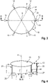
- FIG 2 an equivalent circuit of the antenna array 10 along the lines A-B of Figure 1 is shown, whereas Figure 3 shows a top view on the antenna array 10, thereby revealing that the several antenna elements 12 are arranged in a circumferential manner, namely on a circle.
- the antenna array 10 comprises several loops 14 that are capacitively coupled with the antenna elements 12 via the end(s) of the antenna elements 12.
- the loops 14 are illustrated in Figure 1 by the dashed lines.
- the loops 14 are established by a common base part 16, a common cover part 18 located opposite to the common base part 16 as well as joint elements 20 that interconnect the base part 16 and the cover part 18 with each other.
- the several loops 14 are located within the circular array established by the several antenna elements 12.
- the antenna elements 12 are located along a shell surface of a cylinder that encompasses a space in which the loops 14 are located, thereby ensuring a compact antenna array 10.
- the joint elements 20 of the loops 14 are also located on a shell surface of a cylinder that, however, has a smaller radius compared to the one associated with the antenna elements 12.
- the respective cylinders associated with the antenna elements 12 and the joint elements 20 respectively have a common symmetry axis A as shown in Figures 1 to 3 .
- the symmetry axis A corresponds to the center axis of the antenna array 10.
- Figure 3 further reveals that the common cover part 18 covers the loops 14 in a top view on the antenna array 10, whereas the antenna elements 12 are distanced from the loops 14 in a radial manner. Accordingly, the antenna elements 12 are not covered by the common cover part 18 in the top view on the antenna array 10.
- the capacitive coupling between the antenna elements 12 and the loops 14 may be established by a discrete component 22, for instance a separately formed capacitor as shown in Figure 1 , which is connected with the ends of the antenna elements 12 and the loops 14, particularly the common base part 16 and/or the common cover part 18.
- the capacitive coupling between the antenna elements 12 and the loops 14 may be established by a certain distance or rather gap provided between the antenna elements 12 and the respective loop 14, particularly the common base part 16 and/or the common cover part 18, such that the space provided ensures the capacitive coupling.
- joint elements 20 associated with each of the antenna elements 12 may have at least one terminal port 24 labeled with "a” and "b” in the embodiment shown in Figure 1 .
- the terminal ports 24 may also be called coupling ends or rather coupling points, as they are used for coupling signal voltages processed by the loops 14.
- the signal voltages may be coupled into the loops 14 via the terminal ports 24 for transmission purposes.
- the signal voltages are coupled from the loops 14 via the terminal ports 24 for receiving purposes. Accordingly, this depends on the respective operation mode of the antenna array 10, particularly the loops 14.
- the terminal ports 24 are connected with coupling elements 26, for instance transformers and/or amplifiers.
- the terminal ports 24 (together with the coupling elements 26) are dimensioned such that an equivalent impedance effective at the respective terminal port(s) 24 supports the directivity of the antenna elements 12 as well as the directivity of the loops 14.
- the equivalent impedance labeled with Z s in Figure 2 ensures that electrical and magnetic field components are decoupled in substantially equal portions, resulting in the substantially cardioid directional pattern.
- the coupling elements 26 of the loops 14 are made in a similar manner, wherein they are dimensioned such that the impedance effective at the terminal ports 24 of the joint elements 20 influence the directional pattern of the loops 24 and the antenna elements 12 as mentioned above.
- the antenna elements 12 also comprise coupling members 27 used for coupling antenna voltages.
- the antenna voltages may be coupled into the antenna elements 12 via the coupling members 27 for transmission purposes.
- the antenna voltages are coupled from the antenna elements 12 via the coupling members 27 for receiving purposes. Accordingly, this depends on the respective operation mode of the antenna array 10.
- the antenna elements 12 are capacitively coupled with the loops 14 such that a superimposition of a portion proportional to the electrical field (E-field) and a portion proportional to the magnetic field (H-field) is provided at the respective ports of the antenna elements 12.
- the antenna elements 12 also comprise additional impedance elements 28 that reduce parasitic influences of the antenna elements 12 with respect to each other. Accordingly, the additional impedance elements 28 prevent disturbing resonances that may effect the directional pattern.
- the number of joint elements 20 is an integer multiple or an integer fraction of the number of antenna elements 12, wherein an even number of antenna elements 12 is provided.
- the number of joint elements 20 is twice the number of the antenna elements 12, as a single joint element 20 extends from the common base part 16 towards the coupling member 26 or rather from the common cover part 18 towards the coupling member 26.
- each antenna element 12 has an opposing antenna element 12 which are interconnected via the dedicated loop 14.
- the antenna elements 12 coupled with one loop 14, namely the opposing antenna elements 12, as well as the respective loop 14 are located in a common antenna plane P, wherein the antenna planes P for the respective pairs are illustrated by the dashed lines in Figure 3 .
- the antenna elements 12 are established as dipole antenna elements such that they are coupled with the respective loops 14 via their opposite ends 30.
- the antenna array 10 comprises monopole antenna elements instead of the dipole antenna elements shown in Figure 1 .
- the antenna elements 12 are capacitively connected only via their single end with the respective loops 14.
- the other ends of the monopole antenna elements are grounded on a common ground that is established by the base part 16.
- Figure 5 the overview of Figure 2 is shown for a different embodiment, as a subtraction circuit 32 is provided that interconnects terminal ports 24 of joint elements 20 that are located opposite to each other with respect to the symmetry axis A.
- the subtraction circuit 32 may be established by a transformer, for instance a differential transformer.
- the subtraction circuit 32 interconnected between the opposite orientated terminal ports 24 ensures that a sinusoidal directional pattern of the antenna array 10, particularly the loops 14, is provided that can be used for direction finding purposes, particularly according to the Watson-Watt approach.
- a common printed circuit board 34 is provided to which the antenna elements 12 and the loops 14 are connected. In fact, the antenna elements 12 as well as the loops 14 are located on the common printed circuit board 34.
- the common printed circuit board 34 is provided in a symmetry plane S such that its influence on the radiation pattern is minimized.
- FIG. 7 another embodiment is shown in which the loops 14 and the corresponding antenna elements 12 are connected with a separator filter 36, thereby ensuring that the antenna array 10 is enabled to cover extremely wide frequency bands.
- FIG 8 another embodiment is shown that comprises the common printed circuit board 34 as well as additional antenna elements 38 located on top of the common cover part 18, namely the side of the common cover part 18 that faces away from the common base part 16.
- an internal cable guide 40 for instance established by a tube, is provided that extends along the symmetry axis A of the antenna array 10.
- a ferrite component 42 is provided that encircles the cable guide 40, thereby protecting the antenna elements 12 and the loops 14 effectively against any influences of the cables or rather lines guided along the cable guide 40.
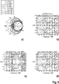
- Figures 9a and 9b illustrate the frequency and azimuth dependency of the antenna array 10 when interconnecting the antenna elements 12 and the loops 14 via the separator filter 38 such that a single output is provided. Particularly, Figure 9a illustrates the horizontal directional pattern for the respective frequencies labelled in the legend, whereas Figure 9b provides an overview of the directional pattern of the entire antenna array 10 in dependency of the frequency.
- Figure 9c shows the directional pattern in dependency of the frequency for the loops 14 separately, whereas Figure 9d shows the directional pattern in dependency of the frequency for the antenna elements 12 separately.
- Figure 9 reveals that improved omnidirectional characteristics at low frequencies are realized for higher gain and/or sensitivity values as well as a continuous transition to directional antenna patterns with increasing frequency.
- the antenna array 10 has broadband/wideband characteristics while ensuring constant directional characteristics and acceptable sensitivity.
Landscapes
- Variable-Direction Aerials And Aerial Arrays (AREA)
Priority Applications (1)
| Application Number | Priority Date | Filing Date | Title |
|---|---|---|---|
| EP20200544.3A EP3982484B1 (de) | 2020-10-07 | 2020-10-07 | Breitbandige gruppenantenne |
Applications Claiming Priority (1)
| Application Number | Priority Date | Filing Date | Title |
|---|---|---|---|
| EP20200544.3A EP3982484B1 (de) | 2020-10-07 | 2020-10-07 | Breitbandige gruppenantenne |
Publications (2)
| Publication Number | Publication Date |
|---|---|
| EP3982484A1 true EP3982484A1 (de) | 2022-04-13 |
| EP3982484B1 EP3982484B1 (de) | 2025-06-04 |
Family
ID=72801376
Family Applications (1)
| Application Number | Title | Priority Date | Filing Date |
|---|---|---|---|
| EP20200544.3A Active EP3982484B1 (de) | 2020-10-07 | 2020-10-07 | Breitbandige gruppenantenne |
Country Status (1)
| Country | Link |
|---|---|
| EP (1) | EP3982484B1 (de) |
Cited By (1)
| Publication number | Priority date | Publication date | Assignee | Title |
|---|---|---|---|---|
| EP4462597A1 (de) * | 2023-05-08 | 2024-11-13 | Alaris Antennas (Pty) Ltd | Richtungsfindungssystem und gruppenantenne |
Citations (4)
| Publication number | Priority date | Publication date | Assignee | Title |
|---|---|---|---|---|
| US2657312A (en) * | 1951-09-28 | 1953-10-27 | Saranga Cesare | Radio and television antenna |
| GB2261997A (en) * | 1992-02-14 | 1993-06-02 | Kandiah Ganeshmoorthy | Antennas |
| US6211846B1 (en) * | 1998-05-26 | 2001-04-03 | Societe Technique D'application Et De Recherche Electronique | Antenna system for radio direction-finding |
| US9874615B2 (en) * | 2012-04-19 | 2018-01-23 | New York University | Dipole array arrangement |
-
2020
- 2020-10-07 EP EP20200544.3A patent/EP3982484B1/de active Active
Patent Citations (4)
| Publication number | Priority date | Publication date | Assignee | Title |
|---|---|---|---|---|
| US2657312A (en) * | 1951-09-28 | 1953-10-27 | Saranga Cesare | Radio and television antenna |
| GB2261997A (en) * | 1992-02-14 | 1993-06-02 | Kandiah Ganeshmoorthy | Antennas |
| US6211846B1 (en) * | 1998-05-26 | 2001-04-03 | Societe Technique D'application Et De Recherche Electronique | Antenna system for radio direction-finding |
| US9874615B2 (en) * | 2012-04-19 | 2018-01-23 | New York University | Dipole array arrangement |
Non-Patent Citations (1)
| Title |
|---|
| LIN WEI ET AL: "Electrically Small, Low-Profile, Huygens Circularly Polarized Antenna", IEEE TRANSACTIONS ON ANTENNAS AND PROPAGATION, IEEE SERVICE CENTER, PISCATAWAY, NJ, US, vol. 66, no. 2, 1 February 2018 (2018-02-01), pages 636 - 643, XP011676781, ISSN: 0018-926X, [retrieved on 20180201], DOI: 10.1109/TAP.2017.2784432 * |
Cited By (2)
| Publication number | Priority date | Publication date | Assignee | Title |
|---|---|---|---|---|
| EP4462597A1 (de) * | 2023-05-08 | 2024-11-13 | Alaris Antennas (Pty) Ltd | Richtungsfindungssystem und gruppenantenne |
| NL2034779B1 (en) * | 2023-05-08 | 2024-11-25 | Alaris Antennas Pty Ltd | Direction finding system and antenna array |
Also Published As
| Publication number | Publication date |
|---|---|
| EP3982484B1 (de) | 2025-06-04 |
Similar Documents
| Publication | Publication Date | Title |
|---|---|---|
| US5038151A (en) | Simultaneous transmit and receive antenna | |
| US12381325B2 (en) | Antenna radiator with pre-configured cloaking to enable dense placement of radiators of multiple bands | |
| US7969372B2 (en) | Antenna apparatus utilizing small loop antenna element having minute length and two feeding points | |
| JP3464277B2 (ja) | 円偏波パッチアンテナ | |
| US11677139B2 (en) | Base station antennas having arrays of radiating elements with 4 ports without usage of diplexers | |
| US6639558B2 (en) | Multi frequency stacked patch antenna with improved frequency band isolation | |
| US6653982B2 (en) | Flat antenna for mobile satellite communication | |
| US6140972A (en) | Multiport antenna | |
| US6812902B2 (en) | Low profile two-antenna assembly having a ring antenna and a concentrically-located monopole antenna | |
| US4649391A (en) | Monopulse cavity-backed multipole antenna system | |
| US20060270368A1 (en) | Integrated Front End Antenna | |
| US8416141B2 (en) | Dual polarised radiating element for cellular base station antennas | |
| US9847582B2 (en) | Wideband simultaneous transmit and receive (STAR) antenna with miniaturized TEM horn elements | |
| US20180145400A1 (en) | Antenna | |
| US20220209387A1 (en) | Differential fed dual polarized tightly coupled dielectric cavity radiator for electronically scanned array applications | |
| CN113708051A (zh) | 辐射单元、天线及基站 | |
| JP3489985B2 (ja) | アンテナ装置 | |
| US4633265A (en) | Low frequency/high frequency omnidirectional antenna formed of plural dipoles extending from a common center | |
| EP3982484B1 (de) | Breitbandige gruppenantenne | |
| US4584582A (en) | Multi-mode direction finding antenna | |
| US6947006B2 (en) | Colinear antenna of the alternating coaxial type | |
| US10673148B1 (en) | Circularly symmetric tightly coupled dipole array with non-coincident phase center | |
| JP2024547120A (ja) | 2つの双極子アレイを有するアンテナデバイス及び関連する通信システム | |
| JP2648453B2 (ja) | 円偏波セルフダイプレクシングアンテナ | |
| CN116169472A (zh) | 叠置微带天线组件及组合天线盒子 |
Legal Events
| Date | Code | Title | Description |
|---|---|---|---|
| PUAI | Public reference made under article 153(3) epc to a published international application that has entered the european phase |
Free format text: ORIGINAL CODE: 0009012 |
|
| STAA | Information on the status of an ep patent application or granted ep patent |
Free format text: STATUS: THE APPLICATION HAS BEEN PUBLISHED |
|
| AK | Designated contracting states |
Kind code of ref document: A1 Designated state(s): AL AT BE BG CH CY CZ DE DK EE ES FI FR GB GR HR HU IE IS IT LI LT LU LV MC MK MT NL NO PL PT RO RS SE SI SK SM TR |
|
| STAA | Information on the status of an ep patent application or granted ep patent |
Free format text: STATUS: REQUEST FOR EXAMINATION WAS MADE |
|
| 17P | Request for examination filed |
Effective date: 20220908 |
|
| RBV | Designated contracting states (corrected) |
Designated state(s): AL AT BE BG CH CY CZ DE DK EE ES FI FR GB GR HR HU IE IS IT LI LT LU LV MC MK MT NL NO PL PT RO RS SE SI SK SM TR |
|
| P01 | Opt-out of the competence of the unified patent court (upc) registered |
Effective date: 20230525 |
|
| GRAP | Despatch of communication of intention to grant a patent |
Free format text: ORIGINAL CODE: EPIDOSNIGR1 |
|
| STAA | Information on the status of an ep patent application or granted ep patent |
Free format text: STATUS: GRANT OF PATENT IS INTENDED |
|
| INTG | Intention to grant announced |
Effective date: 20250321 |
|
| GRAS | Grant fee paid |
Free format text: ORIGINAL CODE: EPIDOSNIGR3 |
|
| GRAA | (expected) grant |
Free format text: ORIGINAL CODE: 0009210 |
|
| STAA | Information on the status of an ep patent application or granted ep patent |
Free format text: STATUS: THE PATENT HAS BEEN GRANTED |
|
| RBV | Designated contracting states (corrected) |
Designated state(s): AL AT BE BG CY CZ DE DK EE ES FI FR GB GR HR HU IS IT LT LU LV MC MK MT NL NO PL PT RO RS SE SI SK SM TR |
|
| AK | Designated contracting states |
Kind code of ref document: B1 Designated state(s): AL AT BE BG CY CZ DE DK EE ES FI FR GB GR HR HU IS IT LT LU LV MC MK MT NL NO PL PT RO RS SE SI SK SM TR |
|
| REG | Reference to a national code |
Ref country code: GB Ref legal event code: FG4D |
|
| REG | Reference to a national code |
Ref country code: DE Ref legal event code: R096 Ref document number: 602020052212 Country of ref document: DE |
|
| REG | Reference to a national code |
Ref country code: NL Ref legal event code: MP Effective date: 20250604 |
|
| PG25 | Lapsed in a contracting state [announced via postgrant information from national office to epo] |
Ref country code: ES Free format text: LAPSE BECAUSE OF FAILURE TO SUBMIT A TRANSLATION OF THE DESCRIPTION OR TO PAY THE FEE WITHIN THE PRESCRIBED TIME-LIMIT Effective date: 20250604 Ref country code: FI Free format text: LAPSE BECAUSE OF FAILURE TO SUBMIT A TRANSLATION OF THE DESCRIPTION OR TO PAY THE FEE WITHIN THE PRESCRIBED TIME-LIMIT Effective date: 20250604 |
|
| REG | Reference to a national code |
Ref country code: LT Ref legal event code: MG9D |
|
| PG25 | Lapsed in a contracting state [announced via postgrant information from national office to epo] |
Ref country code: NO Free format text: LAPSE BECAUSE OF FAILURE TO SUBMIT A TRANSLATION OF THE DESCRIPTION OR TO PAY THE FEE WITHIN THE PRESCRIBED TIME-LIMIT Effective date: 20250904 Ref country code: GR Free format text: LAPSE BECAUSE OF FAILURE TO SUBMIT A TRANSLATION OF THE DESCRIPTION OR TO PAY THE FEE WITHIN THE PRESCRIBED TIME-LIMIT Effective date: 20250905 |
|
| PG25 | Lapsed in a contracting state [announced via postgrant information from national office to epo] |
Ref country code: PL Free format text: LAPSE BECAUSE OF FAILURE TO SUBMIT A TRANSLATION OF THE DESCRIPTION OR TO PAY THE FEE WITHIN THE PRESCRIBED TIME-LIMIT Effective date: 20250604 |
|
| PG25 | Lapsed in a contracting state [announced via postgrant information from national office to epo] |
Ref country code: BG Free format text: LAPSE BECAUSE OF FAILURE TO SUBMIT A TRANSLATION OF THE DESCRIPTION OR TO PAY THE FEE WITHIN THE PRESCRIBED TIME-LIMIT Effective date: 20250604 |
|
| PG25 | Lapsed in a contracting state [announced via postgrant information from national office to epo] |
Ref country code: HR Free format text: LAPSE BECAUSE OF FAILURE TO SUBMIT A TRANSLATION OF THE DESCRIPTION OR TO PAY THE FEE WITHIN THE PRESCRIBED TIME-LIMIT Effective date: 20250604 |
|
| PG25 | Lapsed in a contracting state [announced via postgrant information from national office to epo] |
Ref country code: RS Free format text: LAPSE BECAUSE OF FAILURE TO SUBMIT A TRANSLATION OF THE DESCRIPTION OR TO PAY THE FEE WITHIN THE PRESCRIBED TIME-LIMIT Effective date: 20250904 |
|
| PG25 | Lapsed in a contracting state [announced via postgrant information from national office to epo] |
Ref country code: LV Free format text: LAPSE BECAUSE OF FAILURE TO SUBMIT A TRANSLATION OF THE DESCRIPTION OR TO PAY THE FEE WITHIN THE PRESCRIBED TIME-LIMIT Effective date: 20250604 |
|
| PG25 | Lapsed in a contracting state [announced via postgrant information from national office to epo] |
Ref country code: NL Free format text: LAPSE BECAUSE OF FAILURE TO SUBMIT A TRANSLATION OF THE DESCRIPTION OR TO PAY THE FEE WITHIN THE PRESCRIBED TIME-LIMIT Effective date: 20250604 |
|
| PG25 | Lapsed in a contracting state [announced via postgrant information from national office to epo] |
Ref country code: PT Free format text: LAPSE BECAUSE OF FAILURE TO SUBMIT A TRANSLATION OF THE DESCRIPTION OR TO PAY THE FEE WITHIN THE PRESCRIBED TIME-LIMIT Effective date: 20251006 |
|
| REG | Reference to a national code |
Ref country code: AT Ref legal event code: MK05 Ref document number: 1801305 Country of ref document: AT Kind code of ref document: T Effective date: 20250604 |
|
| PG25 | Lapsed in a contracting state [announced via postgrant information from national office to epo] |
Ref country code: IS Free format text: LAPSE BECAUSE OF FAILURE TO SUBMIT A TRANSLATION OF THE DESCRIPTION OR TO PAY THE FEE WITHIN THE PRESCRIBED TIME-LIMIT Effective date: 20251004 |
|
| PGFP | Annual fee paid to national office [announced via postgrant information from national office to epo] |
Ref country code: DE Payment date: 20251020 Year of fee payment: 6 |
|
| PGFP | Annual fee paid to national office [announced via postgrant information from national office to epo] |
Ref country code: GB Payment date: 20251024 Year of fee payment: 6 |
|
| PG25 | Lapsed in a contracting state [announced via postgrant information from national office to epo] |
Ref country code: AT Free format text: LAPSE BECAUSE OF FAILURE TO SUBMIT A TRANSLATION OF THE DESCRIPTION OR TO PAY THE FEE WITHIN THE PRESCRIBED TIME-LIMIT Effective date: 20250604 Ref country code: SM Free format text: LAPSE BECAUSE OF FAILURE TO SUBMIT A TRANSLATION OF THE DESCRIPTION OR TO PAY THE FEE WITHIN THE PRESCRIBED TIME-LIMIT Effective date: 20250604 |
|
| PGFP | Annual fee paid to national office [announced via postgrant information from national office to epo] |
Ref country code: FR Payment date: 20251027 Year of fee payment: 6 |
|
| PG25 | Lapsed in a contracting state [announced via postgrant information from national office to epo] |
Ref country code: CZ Free format text: LAPSE BECAUSE OF FAILURE TO SUBMIT A TRANSLATION OF THE DESCRIPTION OR TO PAY THE FEE WITHIN THE PRESCRIBED TIME-LIMIT Effective date: 20250604 |
|
| PG25 | Lapsed in a contracting state [announced via postgrant information from national office to epo] |
Ref country code: EE Free format text: LAPSE BECAUSE OF FAILURE TO SUBMIT A TRANSLATION OF THE DESCRIPTION OR TO PAY THE FEE WITHIN THE PRESCRIBED TIME-LIMIT Effective date: 20250604 |
|
| PG25 | Lapsed in a contracting state [announced via postgrant information from national office to epo] |
Ref country code: RO Free format text: LAPSE BECAUSE OF FAILURE TO SUBMIT A TRANSLATION OF THE DESCRIPTION OR TO PAY THE FEE WITHIN THE PRESCRIBED TIME-LIMIT Effective date: 20250604 Ref country code: SK Free format text: LAPSE BECAUSE OF FAILURE TO SUBMIT A TRANSLATION OF THE DESCRIPTION OR TO PAY THE FEE WITHIN THE PRESCRIBED TIME-LIMIT Effective date: 20250604 |
|
| PG25 | Lapsed in a contracting state [announced via postgrant information from national office to epo] |
Ref country code: IT Free format text: LAPSE BECAUSE OF FAILURE TO SUBMIT A TRANSLATION OF THE DESCRIPTION OR TO PAY THE FEE WITHIN THE PRESCRIBED TIME-LIMIT Effective date: 20250604 |
|
| REG | Reference to a national code |
Ref country code: DE Ref legal event code: R097 Ref document number: 602020052212 Country of ref document: DE |
|
| PLBE | No opposition filed within time limit |
Free format text: ORIGINAL CODE: 0009261 |
|
| STAA | Information on the status of an ep patent application or granted ep patent |
Free format text: STATUS: NO OPPOSITION FILED WITHIN TIME LIMIT |
|
| PG25 | Lapsed in a contracting state [announced via postgrant information from national office to epo] |
Ref country code: DK Free format text: LAPSE BECAUSE OF FAILURE TO SUBMIT A TRANSLATION OF THE DESCRIPTION OR TO PAY THE FEE WITHIN THE PRESCRIBED TIME-LIMIT Effective date: 20250604 |