EP3982380A1 - Electronic device and power converter - Google Patents
Electronic device and power converter Download PDFInfo
- Publication number
- EP3982380A1 EP3982380A1 EP21193373.4A EP21193373A EP3982380A1 EP 3982380 A1 EP3982380 A1 EP 3982380A1 EP 21193373 A EP21193373 A EP 21193373A EP 3982380 A1 EP3982380 A1 EP 3982380A1
- Authority
- EP
- European Patent Office
- Prior art keywords
- loop circuit
- layer
- circuit
- electronic device
- disposed
- Prior art date
- Legal status (The legal status is an assumption and is not a legal conclusion. Google has not performed a legal analysis and makes no representation as to the accuracy of the status listed.)
- Pending
Links
Images











Classifications
-
- H—ELECTRICITY
- H01—ELECTRIC ELEMENTS
- H01F—MAGNETS; INDUCTANCES; TRANSFORMERS; SELECTION OF MATERIALS FOR THEIR MAGNETIC PROPERTIES
- H01F19/00—Fixed transformers or mutual inductances of the signal type
- H01F19/04—Transformers or mutual inductances suitable for handling frequencies considerably beyond the audio range
-
- H—ELECTRICITY
- H02—GENERATION; CONVERSION OR DISTRIBUTION OF ELECTRIC POWER
- H02M—APPARATUS FOR CONVERSION BETWEEN AC AND AC, BETWEEN AC AND DC, OR BETWEEN DC AND DC, AND FOR USE WITH MAINS OR SIMILAR POWER SUPPLY SYSTEMS; CONVERSION OF DC OR AC INPUT POWER INTO SURGE OUTPUT POWER; CONTROL OR REGULATION THEREOF
- H02M7/00—Conversion of AC power input into DC power output; Conversion of DC power input into AC power output
- H02M7/42—Conversion of DC power input into AC power output without possibility of reversal
- H02M7/44—Conversion of DC power input into AC power output without possibility of reversal by static converters
- H02M7/48—Conversion of DC power input into AC power output without possibility of reversal by static converters using discharge tubes with control electrode or semiconductor devices with control electrode
- H02M7/53—Conversion of DC power input into AC power output without possibility of reversal by static converters using discharge tubes with control electrode or semiconductor devices with control electrode using devices of a triode or transistor type requiring continuous application of a control signal
- H02M7/537—Conversion of DC power input into AC power output without possibility of reversal by static converters using discharge tubes with control electrode or semiconductor devices with control electrode using devices of a triode or transistor type requiring continuous application of a control signal using semiconductor devices only, e.g. single switched pulse inverters
-
- H—ELECTRICITY
- H01—ELECTRIC ELEMENTS
- H01F—MAGNETS; INDUCTANCES; TRANSFORMERS; SELECTION OF MATERIALS FOR THEIR MAGNETIC PROPERTIES
- H01F27/00—Details of transformers or inductances, in general
- H01F27/28—Coils; Windings; Conductive connections
- H01F27/2804—Printed windings
-
- H—ELECTRICITY
- H01—ELECTRIC ELEMENTS
- H01F—MAGNETS; INDUCTANCES; TRANSFORMERS; SELECTION OF MATERIALS FOR THEIR MAGNETIC PROPERTIES
- H01F27/00—Details of transformers or inductances, in general
- H01F27/34—Special means for preventing or reducing unwanted electric or magnetic effects, e.g. no-load losses, reactive currents, harmonics, oscillations, leakage fields
- H01F27/343—Preventing or reducing surge voltages; oscillations
-
- H—ELECTRICITY
- H02—GENERATION; CONVERSION OR DISTRIBUTION OF ELECTRIC POWER
- H02M—APPARATUS FOR CONVERSION BETWEEN AC AND AC, BETWEEN AC AND DC, OR BETWEEN DC AND DC, AND FOR USE WITH MAINS OR SIMILAR POWER SUPPLY SYSTEMS; CONVERSION OF DC OR AC INPUT POWER INTO SURGE OUTPUT POWER; CONTROL OR REGULATION THEREOF
- H02M7/00—Conversion of AC power input into DC power output; Conversion of DC power input into AC power output
- H02M7/003—Constructional details, e.g. physical layout, assembly, wiring or busbar connections
-
- H—ELECTRICITY
- H01—ELECTRIC ELEMENTS
- H01F—MAGNETS; INDUCTANCES; TRANSFORMERS; SELECTION OF MATERIALS FOR THEIR MAGNETIC PROPERTIES
- H01F27/00—Details of transformers or inductances, in general
- H01F27/28—Coils; Windings; Conductive connections
- H01F27/2804—Printed windings
- H01F2027/2809—Printed windings on stacked layers
-
- H—ELECTRICITY
- H02—GENERATION; CONVERSION OR DISTRIBUTION OF ELECTRIC POWER
- H02M—APPARATUS FOR CONVERSION BETWEEN AC AND AC, BETWEEN AC AND DC, OR BETWEEN DC AND DC, AND FOR USE WITH MAINS OR SIMILAR POWER SUPPLY SYSTEMS; CONVERSION OF DC OR AC INPUT POWER INTO SURGE OUTPUT POWER; CONTROL OR REGULATION THEREOF
- H02M1/00—Details of apparatus for conversion
- H02M1/0083—Converters characterised by their input or output configuration
- H02M1/0085—Partially controlled bridges
Definitions
- One aspect of the present invention relates to an electronic device and a power converter.
- a power converter In a power converter, operations of a high-side semiconductor element and a low-side semiconductor element are periodically switched to periodically change a direction of a current flowing in the power converter.
- the operations of the high-side semiconductor element and the low-side semiconductor element are switched, there is a possibility that a surge or ringing occurs in the power converter.
- the surge or the ringing occurs in the power converter, devices around the power converter are affected by electromagnetic noise due to the surge or the ringing.
- an electronic device has a primary loop circuit that includes a main circuit causing a current to flow in a loop shape; and a secondary loop circuit that is disposed to face the primary loop circuit at a predetermined distance, and causes an induced current generated by a magnetic field generated in the primary loop circuit to flow in a loop shape.
- FIG. 1 shows a schematic perspective view and a cross-sectional view of an electronic device 2 including a power converter 1 according to an example.
- the power converter 1 is a device (including a switch) that converts power.
- the electronic device 2 includes the power converter 1.
- the electronic device 2 of FIG. 1 is configured by disposing the power converter 1 on a base substrate 3.
- the base substrate 3 is, for example, an insulating substrate, and a printed wiring board or the like may be the base substrate 3.
- the electronic device 2 of FIG. 1 includes a primary loop circuit 4 and a secondary loop circuit 5.
- the primary loop circuit 4 includes a main circuit that causes a current to flow in a loop shape.
- the main circuit is a circuit configuring the power converter 1.
- the main circuit has a current path through which a current flows in a loop shape.
- a specific shape of the current path is arbitrary, and may be a meandering shape.
- a specific circuit configuration of the main circuit will be described later.
- the primary loop circuit 4 is not necessarily a circuit configuring the power converter 1.
- the primary loop circuit 4 may be any circuit having a current path through which a current flows in a loop shape.
- the secondary loop circuit 5 is disposed to face the primary loop circuit 4 at a predetermined distance, and causes an induced current to flow in a loop shape.
- the secondary loop circuit 5 does not include an active element such as a transistor and a diode, but includes a passive element.
- the secondary loop circuit 5 causes an induced current generated by an influence of a magnetic field caused by the current flowing in the primary loop circuit 4 to flow.
- the secondary loop circuit 5 desirably has a shape and size corresponding to the shape and the size of the primary loop circuit 4. More desirably, the primary loop circuit 4 has substantially the same shape and size as those of the secondary loop circuit 5.
- the secondary loop circuit 5 configures a loop antenna receiving power from the primary loop circuit 4.
- the predetermined distance is a distance within a range in which the induced current generated by a magnetic field generated in the main circuit flows in the secondary loop circuit 5. That is, the predetermined distance is a distance within a range in which the secondary loop circuit 5 is magnetically coupled to the primary loop circuit 4.
- a first layer 6 in which the primary loop circuit 4 is disposed and a second layer 7 in which the secondary loop circuit 5 is disposed are provided on the base substrate 3.
- the second layer 7 is disposed above or below the first layer 6 at a predetermined distance.
- the first layer 6 and the second layer 7 are disposed on a front surface, a back surface, or an inner layer surface of the base substrate 3.
- the primary loop circuit 4 and at least a part of the secondary loop circuit 5 are disposed so as to vertically overlap each other.
- the first layer 6 in which the primary loop circuit 4 is disposed is disposed on a first insulation layer 8
- the second layer 7 in which the secondary loop circuit 5 is disposed is disposed on a second insulation layer 9 below the first insulation layer 8
- the second insulation layer 9 is disposed on the base substrate 3.
- a stacked structure of the electronic device 2 of FIG. 1 is an example, and various modified examples can be considered.
- a stacking order of the first layer 6 and the second layer 7 may be reversed.
- the first layer 6 may be disposed on a first main surface of the base substrate 3
- the second layer 7 may be disposed on a second main surface on an opposite side to the first main surface of the base substrate 3.
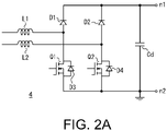
- FIG. 2A is a circuit diagram illustrating an example of the primary loop circuit 4 disposed in the first layer 6.
- FIG. 2A is a circuit diagram of the power converter 1.
- the power converter 1 of FIG. 2A includes a high-side semiconductor element D1 and a low-side semiconductor element Q1 which are connected in series between a first node n1 and a second node n2, a high-side semiconductor element D2 and a low-side semiconductor element Q2 which are also connected in series between the first node n1 and the second node n2, a capacitor Cd connected between the first node n1 and the second node n2, a first inductor L1, and a second inductor L2.
- Each of the high-side semiconductor elements D1 and D2, and the low-side semiconductor elements Q1 and Q2 is a transistor or a diode.
- FIG. 2A illustrates an example in which the high-side semiconductor elements D1 and D2 are diodes, and the low-side semiconductor elements Q1 and Q2 are transistors.
- FIG. 2B is a diagram illustrating directions of currents flowing in the power converter 1 by arrow lines in a case where the low-side semiconductor element Q1 is turned on and in a case where the low-side semiconductor element Q1 is turned off.
- a circuit CT1 of FIG. 2B illustrates a current path in a case where the low-side semiconductor element Q1 in the power converter 1 of FIG. 2A is turned on. In this case, the current flows in the first inductor L1, the low-side semiconductor element Q1, a diode D4 connected in parallel with a low-side transistor Q2, and the second inductor L2 in this order.
- a circuit CT2 of FIG. 2B illustrates a current path in a case where the low-side semiconductor element Q1 is turned off. In this case, the current flows in the first inductor L1, the high-side semiconductor element D1, the capacitor Cd, the diode D4 connected in parallel with the low-side semiconductor element Q2, and the second inductor L2 in this order.
- the circuit CT1 of FIG. 2B is substantially equivalent to a circuit CT3 of FIG. 2C .
- the circuit CT3 is a circuit diagram in which a part of the circuit CT1 is changed without changing a circuit operation, and a connection position of the low-side semiconductor element Q2 and the second inductor L2 is changed.
- circuit CT2 of FIG. 2B is substantially equivalent to a circuit CT4 of FIG. 2C .
- the circuit CT4 is a circuit diagram in which a part of the circuit CT2 is changed without changing a circuit operation, and a connection position of the low-side semiconductor element Q2 and the second inductor L2 is changed.
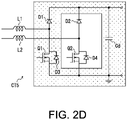
- a loop-shaped current path indicated by a shaded portion of FIG. 2D is formed in a transient state in which the low-side semiconductor element Q1 is switched from on to off or from off to on.
- the current path may be referred to as a first current path.
- a circuit having a loop-shaped current path is referred to as a primary loop circuit 4.
- 2E is a diagram illustrating a waveform of each of a voltage VD1 between opposite ends of the high-side semiconductor element (diode) D1, a drain-source voltage VQ1 of the low-side semiconductor element Q1, and a drain current IQ1 of the low-side semiconductor element Q1 in an off-period, an on-period, and a transient state period between the off-period and the on-period of the low-side semiconductor element Q1 in the power converter 1 of FIG. 2A .
- the current flows along the loop-shaped current path of FIG. 2D , and a surge and ringing occur.
- FIG. 2F is a circuit diagram illustrating a circuit CT6 equivalent to a circuit CT5 of FIG. 2D .
- the circuit CT6 of FIG. 2F is obtained by changing a connection position of the capacitor Cd in the circuit CT5 of FIG. 2D .
- the low-side semiconductor elements Q1 and Q2 in the circuit CT6 of FIG. 2F are alternately turned on and off, and the current path similar to the current path of FIG. 2D is formed. As described above, even when the low-side semiconductor elements Q1 and Q2 are alternately turned on and off, the current path similar to that of FIG. 2D is formed. Therefore, in the example, analysis by simulation is performed assuming that the power converter 1 includes the primary loop circuit 4 having the current path of FIG. 2D .
- FIG. 3 is a diagram illustrating a feature of the primary loop circuit 4.
- the circuit CT5 having the current path of FIG. 2D is equivalent to a circuit CT7 illustrated in FIG. 3 .
- the circuit CT7 is a circuit in which the high-side semiconductor element D1, an inductor Ls1, the capacitor Cd, an inductor Ls2, the low-side semiconductor element Q1, an inductor Ls3, and an inductor Ls4 are connected in series.
- the inductors Ls1 to Ls4 are parasitic inductances formed by terminals of circuit components such as the high-side semiconductor element D1, the low-side semiconductor element Q1, and the capacitor Cd.
- the mounting example IM1 illustrates an example in which individual discrete components 11 are mounted as the high-side semiconductor element D1, the low-side semiconductor element Q1, and the capacitor Cd.
- parasitic inductances Ls1 to Ls4 are generated in terminal portions of the mounted discrete components 11.
- the current path is simply represented by a loop-shaped conductive pattern 12. A part of the loop-shaped conductive pattern 12 is cut out, and the capacitor Cd is connected between opposite ends of the cut portion.
- opposite ends of the loop-shaped conductive pattern 12 are referred to as the first node n1 and the second node n2.
- the current path is formed on the conductive pattern 12 extending in a plane direction, whereas the discrete components 11 are disposed in the normal direction from an arrangement surface of the conductive pattern 12.
- a magnetic field corresponding to a direction of the current flowing through the conductive pattern 12 is generated.
- the magnetic field generated in the primary loop circuit 4 is disturbed by the discrete components 11, and the direction of the magnetic field becomes complicated.
- a chip component 13 and a surface mounting component 14 are often adopted as the high-side semiconductor element D1, the low-side semiconductor element Q1, and the capacitor Cd. Since the chip component 13 and the surface mounting component 14 have a low height in the normal direction of the mounting surface, a degree in which the direction of the magnetic field generated by the current flowing through the conductive pattern 12 is disturbed by these components is reduced. Therefore, the direction of the magnetic field generated from the primary loop circuit 4 can be regarded as the normal direction of the mounting surface of the primary loop circuit 4 in defiance of an influence of the mounting component.
- the secondary loop circuit 5 when focusing on the fact that the primary loop circuit 4 configuring the power converter 1 generates a magnetic field in the normal direction of the mounting surface, the secondary loop circuit 5 is disposed in the vicinity of the primary loop circuit 4, and the inductance caused by combining the primary loop circuit 4 and the secondary loop circuit 5 is reduced by magnetically coupling the primary loop circuit 4 to the secondary loop circuit 5. As a result, a surge and ringing generated in the primary loop circuit 4 can be suppressed.
- FIG. 4 shows a schematic external view in which the secondary loop circuit 5 is disposed in the vicinity of the primary loop circuit 4 and an equivalent circuit diagram.
- the secondary loop circuit 5 is disposed above the primary loop circuit 4, but an arrangement order of the primary loop circuit 4 and the secondary loop circuit 5 is arbitrary.
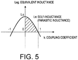
- self-inductances (parasitic inductances) of the primary loop circuit 4 and the secondary loop circuit 5 are both denoted by Ls
- the coupling coefficients of the primary loop circuit 4 and the secondary loop circuit 5 are denoted by k
- a conductor resistance obtained by combining the primary loop circuit 4 and the secondary loop circuit 5 is denoted by r.
- the equivalent circuit of the primary loop circuit 4 and the secondary loop circuit 5 is represented by two inductances (1-k)Ls, one inductance kLs, and a conductor resistance r.
- a coupling coefficient k is a value larger than 0 and smaller than 1.
- the coupling coefficient k changes according to the distance between the primary loop circuit 4 and the secondary loop circuit 5, the closer the distance is, the larger the coupling coefficient k becomes, and the equivalent inductance becomes closer to 0. As the equivalent inductance is smaller, a surge and ringing generated in the primary loop circuit 4 can be suppressed.
- the present inventor verifies how the equivalent inductance changes when the distance between the primary loop circuit 4 and the secondary loop circuit 5 changes, and verifies how the resistance value obtained by combining the primary loop circuit 4 and the secondary loop circuit 5 changes depending on a frequency. These verifications are performed by simulation.
- the resistance value obtained by combining the primary loop circuit 4 and the secondary loop circuit 5 is a resistance value obtained by adding up the conductor resistance of the primary loop circuit 4, the conductor resistance of the secondary loop circuit 5, and the resistance value of an external resistance element Rex connected to the secondary loop circuit 5.
- FIG. 6A is an external view of the electronic device 2 used for simulation.
- the primary loop circuit 4 and the secondary loop circuit 5 have the same size and shape, and are disposed so as to completely and vertically overlap each other at a predetermined distance.
- the primary loop circuit 4 is disposed on the secondary loop circuit 5.
- Dimensions of electrode portions at opposite ends of the primary loop circuit 4 and the secondary loop circuit 5 are 2.5 mm ⁇ 5 mm, and external sizes of the primary loop circuit 4 and the secondary loop circuit 5 are 20 mm ⁇ 20 mm.
- a distance d between the primary loop circuit 4 and the secondary loop circuit 5 is changed in a plurality of ways within a range of 0.1 mm to 1 mm.
- the resistance value of the external resistance element Rex connected between opposite ends of the secondary loop circuit 5 is changed in a plurality of ways.
- FIG. 6B is a graph illustrating a result of the simulation performed by using the electronic device 2 of FIG. 6A .
- FIG. 6B illustrates curves w1 to w4 indicating a relationship between the frequency and an equivalent inductance L when the distance between the primary loop circuit 4 and the secondary loop circuit 5 is changed in a plurality of ways, and curves w5 to w8 indicating a relationship between the frequency and a resistance value R obtained by combining the primary loop circuit 4 and the secondary loop circuit 5.
- the frequency in FIG. 6B is a frequency at which operations of the high-side semiconductor element D1 and D2 and the low-side semiconductor element Q1 and Q2 are switched.
- 6B illustrates a curve obtained in a case where the distance between the primary loop circuit 4 and the secondary loop circuit 5 is 100 ⁇ m, 500 ⁇ m, or 1000 ⁇ m, and a curve obtained in a case where the secondary loop circuit 5 is not provided (denoted by wo coil).
- FIG. 7 is a circuit diagram of the power converter 1, which is input to the circuit simulator.
- the power converter 1 of FIG. 7 includes the primary loop circuit 4 and the secondary loop circuit 5.
- the primary loop circuit 4 includes the diode D1 that is the high-side semiconductor element, the transistor Q1 that is the low-side semiconductor element, the capacitor Cd (DC voltage source), voltmeters 15 and 16, an ammeter 17, an AC voltage source 19, a resistance element R1, a load inductor L12, and a plurality of inductors L11 and L13.
- a plurality of the inductors L11 and L13 are self-inductances of the primary loop circuit 4, which appears at terminals of the circuit components. More specifically, the inductor L13 is an inductance used for magnetic coupling with the secondary loop circuit 5, and the inductor L11 is a parasitic inductance not used for coupling.
- the secondary loop circuit 5 includes a plurality of inductors L14 and L15 and the external resistance element Rex connected between the opposite ends of the secondary loop circuit 5. More specifically, the inductor L14 is an inductance used for magnetic coupling with the primary loop circuit 4, and the inductor L15 is a parasitic inductance not used for coupling.
- FIG. 8A is a graph of a voltage waveform between opposite ends of the diode D1 when the operation of the diode D1, which is the high-side semiconductor element of FIG. 7 , is switched and the current does not flow in the diode D1.
- the voltage waveform is measured by the voltmeter 15 of FIG. 7 .
- FIG. 8A it can be seen that a surge voltage can be further suppressed and ringing can be further suppressed as the resistance value of the external resistance element Rex is larger.
- FIG. 8B is a graph of a drain current waveform of the transistor Q1 when the current does not flow in the diode D1 which is the high-side semiconductor element, that is, when the transistor Q1 which is the low-side semiconductor element is turned on.
- the current waveform is measured by the ammeter 17 of FIG. 7 .
- the larger the resistance value of the external resistance element Rex the smaller the surge and ringing of the drain current.
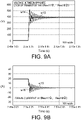
- FIG. 9A is a graph of a voltage waveform of the drain-source voltage when the transistor Q1 which is the low-side semiconductor element of FIG. 7 is turned off.
- the surge voltage hardly changes even when the external resistance element Rex is changed, but the ringing is smaller as the resistance value of the external resistance element Rex is larger.
- FIG. 9B is a graph of the drain current waveform of the transistor Q1 when the transistor Q1, which is the low-side semiconductor element of FIG. 7 , is turned off.
- a surge current hardly changes even when the external resistance element Rex is changed, but the ringing is smaller as the resistance value of the external resistance element Rex is larger.
- the resistance value is a value obtained by adding up the conductor resistance of the primary loop circuit 4, the conductor resistance of the secondary loop circuit 5, and the resistance value of the external resistance element Rex connected to the secondary loop circuit 5.
- FIG. 10 is an equivalent circuit diagram used for verification, and includes two inductances (1-k)Ls, one inductance kLs, the resistance value R, the capacitor Cd (DC voltage source), the diode D1 which is the high-side semiconductor element, a capacitor C1 connected in parallel to the diode D1, and the transistor Q1 which is the low-side semiconductor element, in the similar manner to the equivalent circuit illustrated in FIG. 7 or 4 .
- a switching frequency at which the transistor Q1 is turned on or off is changed in a plurality of ways to examine the frequency at which the impedance becomes minimum.
- Ls is a self-inductance.
- FIG. 11 is a graph illustrating frequency characteristics of an impedance calculated based on Equation (1). More specifically, FIG. 11 is a graph illustrating a waveform indicating the relationship between the switching frequency of the transistor Q1 and the entire impedance in terms of the primary loop circuit 4 in a case where the resistance value obtained by combining the primary loop circuit 4 and the secondary loop circuit 5 is changed in a plurality of ways. A surge voltage and ringing occur at a frequency at which the impedance becomes minimum.
- the minimum value of the impedance tends to decrease as the resistance value decreases, but a result is obtained that a magnitude relationship of the minimum value of the impedance is reversed depending on the resistance value, for example, the minimum value of the impedance is smaller at the resistance value of 20 ohms than at the resistance value R of 50 ohms.
- FIG. 12A is a graph illustrating voltage waveforms w21 to w23 between opposite ends of the diode D1, which is the high-side semiconductor element, when the resistance value R is 1 ohm, 20 ohm, and 50 ohm.
- FIG. 12B is a graph illustrating drain current waveforms w24 to w26 of the transistor Q1, which is the low-side semiconductor element, when the resistance value R is 1 ohm, 20 ohm, and 50 ohm.
- the surge and ringing of the voltage between opposite ends of the diode and the surge and ringing of the drain current of the transistor Q1 are maximized. Furthermore, the surge and ringing of the voltage between opposite ends of the diode and the surge and ringing of the drain current of the transistor Q1 are smaller at the resistance value R of 20 that at the resistance value R of 50. As described above, it is found that the surge and ringing are not necessarily smaller as the resistance value increases.
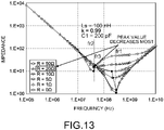
- FIG. 13 is a graph illustrating the waveform indicating the relationship between the switching frequency of the transistor Q1 and the entire impedance in terms of the primary loop circuit 4 in a case where the resistance value obtained by combining the primary loop circuit 4 and the secondary loop circuit 5 is changed in a plurality of ways.
- the minimum value of the impedance exists for any resistance value. As the resistance value R is smaller, the minimum value of the impedance tends to be smaller, but at some resistance values R, the magnitude relationship of the minimum value of the impedance is reversed.
- FIG. 14A is a graph illustrating voltage waveforms w27 to w29 between opposite ends of the diode D1, which is the high-side semiconductor element, when the resistance value R is 1 ohm, 20 ohm, and 50 ohm.
- FIG. 14B is a graph illustrating drain current waveforms w30 to w32 of the transistor Q1, which is the low-side semiconductor element, when the resistance value R is 1 ohm, 20 ohm, and 50 ohm.
- FIGS. 14A and 14B when the resistance value R is 1 ohm, the surge of the voltage between opposite ends of the diode and the surge of the drain current of the transistor Q1 are maximized. However, when the resistance value R is 1 ohm, since a frequency fr1 at which the impedance becomes minimum is higher than a frequency fr2 and a frequency fr3, the ringing occurs in the shortest time. When the resistance value R is 20 ohms, the surge and ringing are smaller than those when resistance value R is 50 ohms.
- the resistance value obtained by combining the primary loop circuit 4 and the secondary loop circuit 5 is a resistance value obtained by adding up the conductor resistance of the primary loop circuit 4, the conductor resistance of the secondary loop circuit 5, and the resistance value of the external resistance element Rex connected to the secondary loop circuit 5.
- a resistance value that can be easily adjusted is a resistance value of the external resistance element Rex. Therefore, the external resistance element Rex is desirably disposed at a position in which the resistance value can be easily adjusted.
- FIG. 15 is a cross-sectional view illustrating an example in which the external resistance element Rex is disposed on the outermost surface layer (first layer 6) in which the primary loop circuit 4 is formed.
- the second layer 7 having the secondary loop circuit 5 is formed on the second insulation layer 9 disposed on the base substrate 3
- the first layer 6 having the primary loop circuit 4 is formed on the first insulation layer 8 disposed on the second layer 7.
- Contacts 21 (first contacts) extending upward from opposite ends of the secondary loop circuit 5 are disposed, and the contacts 21 are connected to the external resistance element Rex disposed on the first insulation layer 8.
- the secondary loop circuit 5, in which a part of the current path is cut out, is disposed so as to surround a part of a region on the second layer 7 from a first end portion to a second end portion of the current path, and opposite ends of the resistance element are connected to the first end portion and the second end portion via separate contacts 21.
- the secondary loop circuit 5 functions as a loop antenna.
- the loop antenna is easily affected by a surrounding magnetic field other than the primary loop circuit 4. Therefore, the shield layer may be disposed on a surface of the secondary loop circuit 5, the surface being opposite to the surface facing the primary loop circuit 4.
- FIG. 16 is a cross-sectional view in which the shield layer 22 (third layer) is added to the configuration of FIG. 15 .
- the shield layer 22 is disposed on a surface of the base substrate 3, the surface being opposite to a contact surface with the first insulation layer 8.
- the shield layer 22 has a solid conductive pattern.
- Contacts 23 extend upward from the shield layer 22, and the contacts 23 are connected to the secondary loop circuit 5 and the primary loop circuit 4.
- the contacts 23 extending upward from the shield layer 22 are connected to a grounding portion of the secondary loop circuit 5 and a grounding portion of the primary loop circuit 4. According to this, it is possible to suppress a potential fluctuation of a ground level of the primary loop circuit 4 and the secondary loop circuit 5.
- the shield layer 22 is disposed on a surface of the base substrate 3, the surface being opposite to a contact surface with the first insulation layer 8, but the shield layer 22 may be disposed between the base substrate 3 and the first insulation layer 8.
- the shield layer 22 may be used as the shield layer 22.
- the shield layer 22 may be brought into contact with a heat sink (not illustrated) or the like. Accordingly, it is possible to dissipate heat from the electronic device 2 and to suppress fluctuation of a ground potential.
- the equivalent inductance caused by combining the primary loop circuit 4 and the secondary loop circuit 5 can be reduced by magnetically coupling the primary loop circuit 4 to the secondary loop circuit 5, and the surge and ringing that occur in the primary loop circuit 4 can be suppressed.
Landscapes
- Engineering & Computer Science (AREA)
- Power Engineering (AREA)
- Multimedia (AREA)
- Dc-Dc Converters (AREA)
- Semiconductor Integrated Circuits (AREA)
Abstract
An electronic device has a primary loop circuit that includes a main circuit causing a current to flow in a loop shape; and a secondary loop circuit that is disposed to face the primary loop circuit at a predetermined distance, and causes an induced current generated by a magnetic field generated in the primary loop circuit to flow in a loop shape.
Description
- One aspect of the present invention relates to an electronic device and a power converter.
- In a power converter, operations of a high-side semiconductor element and a low-side semiconductor element are periodically switched to periodically change a direction of a current flowing in the power converter. When the operations of the high-side semiconductor element and the low-side semiconductor element are switched, there is a possibility that a surge or ringing occurs in the power converter. When the surge or the ringing occurs in the power converter, devices around the power converter are affected by electromagnetic noise due to the surge or the ringing.
- As a quick measure to prevent the electromagnetic noise, it is conceivable to provide a shield plate around the power converter. However, when a place in which the shield plate is disposed is not appropriate, the electromagnetic noise cannot be effectively suppressed. Furthermore, it is conceivable to cover the entire power converter with the shield plate, but cost is increased, and miniaturization becomes difficult.
-
-
FIG. 1 is a schematic perspective view and a cross-sectional view of an electronic device including a power converter according to an example; -
FIG. 2A is a circuit diagram illustrating an example of a primary loop circuit disposed in a first layer; -
FIG. 2B is a diagram illustrating directions of currents flowing in a power converter in a case where a low-side semiconductor element is turned on and in a case where the low-side semiconductor element is turned off by arrow lines; -
FIG. 2C is a circuit diagram in which the circuit ofFIG. 2B is partially changed; -
FIG. 2D is a diagram illustrating a current path when an operation of a semiconductor element of a power converter ofFIG. 2A is switched; -
FIG. 2E is a waveform diagram of a transient state period during which a low-side semiconductor element is switched to be turned on and off; -
FIG. 2F is a circuit diagram illustrating a circuit equivalent to a circuit ofFIG. 2D ; -
FIG. 3 is a diagram illustrating a feature of a primary loop circuit; -
FIG. 4 is a schematic external view in which a secondary loop circuit is disposed in a vicinity of a primary loop circuit and an equivalent circuit diagram; -
FIG. 5 is a diagram illustrating a correspondence relationship between a coupling coefficient and an equivalent inductance; -
FIG. 6A is an external view of an electronic device used for simulation; -
FIG. 6B is a graph illustrating a result of the simulation performed by using the electronic device ofFIG. 6A ; -
FIG. 7 is a circuit diagram of a power converter, which is input to a circuit simulator; -
FIG. 8A is a graph of a voltage waveform between opposite ends of a diode when a current does not flow in the diode; -
FIG. 8B is a graph of a drain current waveform of a low-side semiconductor element when the low-side semiconductor element is turned on; -
FIG. 9A is a graph of a voltage waveform of a drain-source voltage when a low-side semiconductor element ofFIG. 7 is turned off; -
FIG. 9B is a graph of a drain current waveform of a transistor when a low-side semiconductor element ofFIG. 7 is turned off; -
FIG. 10 is an equivalent circuit diagram used for verification; -
FIG. 11 is a graph illustrating frequency characteristics of an impedance; -
FIG. 12A is a graph illustrating a voltage waveform between opposite ends of a diode that is a high-side semiconductor element; -
FIG. 12B is a graph illustrating a drain current waveform of a low-side semiconductor element; -
FIG. 13 is a waveform graph illustrating a relationship between a switching frequency of a transistor and an entire impedance in terms of a primary loop circuit; -
FIG. 14A is a graph illustrating a voltage waveform between opposite ends of a high-side semiconductor element; -
FIG. 14B is a graph illustrating a drain current waveform of a low-side semiconductor element; -
FIG. 15 is a cross-sectional view illustrating an example in which an external resistance element is disposed on an outermost surface layer in which a primary loop circuit is formed; and -
FIG. 16 is a cross-sectional view in which a shield layer is added to a configuration ofFIG. 15 . - According to one example, an electronic device has a primary loop circuit that includes a main circuit causing a current to flow in a loop shape; and a secondary loop circuit that is disposed to face the primary loop circuit at a predetermined distance, and causes an induced current generated by a magnetic field generated in the primary loop circuit to flow in a loop shape.
- Hereinafter, examples of an electronic device and a power converter will be described with reference to the drawings. Main constituent parts of the electronic device and the power converter will be mainly described below, but the electronic device and the power converter may have constituent parts and functions not illustrated or described. The following description does not exclude the constituent parts and the functions not illustrated or described.
-
FIG. 1 shows a schematic perspective view and a cross-sectional view of anelectronic device 2 including apower converter 1 according to an example. Thepower converter 1 is a device (including a switch) that converts power. For example, theelectronic device 2 includes thepower converter 1. Theelectronic device 2 ofFIG. 1 is configured by disposing thepower converter 1 on abase substrate 3. Thebase substrate 3 is, for example, an insulating substrate, and a printed wiring board or the like may be thebase substrate 3. Theelectronic device 2 ofFIG. 1 includes aprimary loop circuit 4 and asecondary loop circuit 5. - The
primary loop circuit 4 includes a main circuit that causes a current to flow in a loop shape. The main circuit is a circuit configuring thepower converter 1. The main circuit has a current path through which a current flows in a loop shape. A specific shape of the current path is arbitrary, and may be a meandering shape. A specific circuit configuration of the main circuit will be described later. Theprimary loop circuit 4 is not necessarily a circuit configuring thepower converter 1. Theprimary loop circuit 4 may be any circuit having a current path through which a current flows in a loop shape. - The
secondary loop circuit 5 is disposed to face theprimary loop circuit 4 at a predetermined distance, and causes an induced current to flow in a loop shape. Thesecondary loop circuit 5 does not include an active element such as a transistor and a diode, but includes a passive element. Thesecondary loop circuit 5 causes an induced current generated by an influence of a magnetic field caused by the current flowing in theprimary loop circuit 4 to flow. Thesecondary loop circuit 5 desirably has a shape and size corresponding to the shape and the size of theprimary loop circuit 4. More desirably, theprimary loop circuit 4 has substantially the same shape and size as those of thesecondary loop circuit 5. Thesecondary loop circuit 5 configures a loop antenna receiving power from theprimary loop circuit 4. - The predetermined distance is a distance within a range in which the induced current generated by a magnetic field generated in the main circuit flows in the
secondary loop circuit 5. That is, the predetermined distance is a distance within a range in which thesecondary loop circuit 5 is magnetically coupled to theprimary loop circuit 4. - As illustrated in
FIG. 1 , afirst layer 6 in which theprimary loop circuit 4 is disposed and asecond layer 7 in which thesecondary loop circuit 5 is disposed are provided on thebase substrate 3. Thesecond layer 7 is disposed above or below thefirst layer 6 at a predetermined distance. Thefirst layer 6 and thesecond layer 7 are disposed on a front surface, a back surface, or an inner layer surface of thebase substrate 3. When thefirst layer 6 and thesecond layer 7 are viewed in a plan view in a normal direction of thefirst layer 6 and thesecond layer 7, theprimary loop circuit 4 and at least a part of thesecondary loop circuit 5 are disposed so as to vertically overlap each other. - In the example of
FIG. 1 , thefirst layer 6 in which theprimary loop circuit 4 is disposed is disposed on afirst insulation layer 8, thesecond layer 7 in which thesecondary loop circuit 5 is disposed is disposed on asecond insulation layer 9 below thefirst insulation layer 8, and thesecond insulation layer 9 is disposed on thebase substrate 3. A stacked structure of theelectronic device 2 ofFIG. 1 is an example, and various modified examples can be considered. For example, a stacking order of thefirst layer 6 and thesecond layer 7 may be reversed. Alternatively, thefirst layer 6 may be disposed on a first main surface of thebase substrate 3, and thesecond layer 7 may be disposed on a second main surface on an opposite side to the first main surface of thebase substrate 3. -
FIG. 2A is a circuit diagram illustrating an example of theprimary loop circuit 4 disposed in thefirst layer 6.FIG. 2A is a circuit diagram of thepower converter 1. Thepower converter 1 ofFIG. 2A includes a high-side semiconductor element D1 and a low-side semiconductor element Q1 which are connected in series between a first node n1 and a second node n2, a high-side semiconductor element D2 and a low-side semiconductor element Q2 which are also connected in series between the first node n1 and the second node n2, a capacitor Cd connected between the first node n1 and the second node n2, a first inductor L1, and a second inductor L2. Each of the high-side semiconductor elements D1 and D2, and the low-side semiconductor elements Q1 and Q2 is a transistor or a diode.FIG. 2A illustrates an example in which the high-side semiconductor elements D1 and D2 are diodes, and the low-side semiconductor elements Q1 and Q2 are transistors. -
FIG. 2B is a diagram illustrating directions of currents flowing in thepower converter 1 by arrow lines in a case where the low-side semiconductor element Q1 is turned on and in a case where the low-side semiconductor element Q1 is turned off. A circuit CT1 ofFIG. 2B illustrates a current path in a case where the low-side semiconductor element Q1 in thepower converter 1 ofFIG. 2A is turned on. In this case, the current flows in the first inductor L1, the low-side semiconductor element Q1, a diode D4 connected in parallel with a low-side transistor Q2, and the second inductor L2 in this order. A circuit CT2 ofFIG. 2B illustrates a current path in a case where the low-side semiconductor element Q1 is turned off. In this case, the current flows in the first inductor L1, the high-side semiconductor element D1, the capacitor Cd, the diode D4 connected in parallel with the low-side semiconductor element Q2, and the second inductor L2 in this order. - The circuit CT1 of
FIG. 2B is substantially equivalent to a circuit CT3 ofFIG. 2C . The circuit CT3 is a circuit diagram in which a part of the circuit CT1 is changed without changing a circuit operation, and a connection position of the low-side semiconductor element Q2 and the second inductor L2 is changed. - Similarly, the circuit CT2 of
FIG. 2B is substantially equivalent to a circuit CT4 ofFIG. 2C . The circuit CT4 is a circuit diagram in which a part of the circuit CT2 is changed without changing a circuit operation, and a connection position of the low-side semiconductor element Q2 and the second inductor L2 is changed. - When focusing on the current flow paths of the circuit CT3 and the circuit CT4 in
FIG. 2C , in thepower converter 1 ofFIG. 2A , a loop-shaped current path indicated by a shaded portion ofFIG. 2D is formed in a transient state in which the low-side semiconductor element Q1 is switched from on to off or from off to on. In the example, the current path may be referred to as a first current path. In the present specification, a circuit having a loop-shaped current path is referred to as aprimary loop circuit 4.FIG. 2E is a diagram illustrating a waveform of each of a voltage VD1 between opposite ends of the high-side semiconductor element (diode) D1, a drain-source voltage VQ1 of the low-side semiconductor element Q1, and a drain current IQ1 of the low-side semiconductor element Q1 in an off-period, an on-period, and a transient state period between the off-period and the on-period of the low-side semiconductor element Q1 in thepower converter 1 ofFIG. 2A . During the transient state period ofFIG. 2E , the current flows along the loop-shaped current path ofFIG. 2D , and a surge and ringing occur. -
FIG. 2F is a circuit diagram illustrating a circuit CT6 equivalent to a circuit CT5 ofFIG. 2D . The circuit CT6 ofFIG. 2F is obtained by changing a connection position of the capacitor Cd in the circuit CT5 ofFIG. 2D . The low-side semiconductor elements Q1 and Q2 in the circuit CT6 ofFIG. 2F are alternately turned on and off, and the current path similar to the current path ofFIG. 2D is formed. As described above, even when the low-side semiconductor elements Q1 and Q2 are alternately turned on and off, the current path similar to that ofFIG. 2D is formed. Therefore, in the example, analysis by simulation is performed assuming that thepower converter 1 includes theprimary loop circuit 4 having the current path ofFIG. 2D . -
FIG. 3 is a diagram illustrating a feature of theprimary loop circuit 4. The circuit CT5 having the current path ofFIG. 2D is equivalent to a circuit CT7 illustrated inFIG. 3 . The circuit CT7 is a circuit in which the high-side semiconductor element D1, an inductor Ls1, the capacitor Cd, an inductor Ls2, the low-side semiconductor element Q1, an inductor Ls3, and an inductor Ls4 are connected in series. The inductors Ls1 to Ls4 are parasitic inductances formed by terminals of circuit components such as the high-side semiconductor element D1, the low-side semiconductor element Q1, and the capacitor Cd. - When the
power converter 1 ofFIG. 2A is mounted as a discrete component, for example, a mounting example IM1 ofFIG. 3 is obtained. The mounting example IM1 illustrates an example in which individualdiscrete components 11 are mounted as the high-side semiconductor element D1, the low-side semiconductor element Q1, and the capacitor Cd. In this case, parasitic inductances Ls1 to Ls4 are generated in terminal portions of the mounteddiscrete components 11. In the mounting example IM1, the current path is simply represented by a loop-shapedconductive pattern 12. A part of the loop-shapedconductive pattern 12 is cut out, and the capacitor Cd is connected between opposite ends of the cut portion. Hereinafter, opposite ends of the loop-shapedconductive pattern 12 are referred to as the first node n1 and the second node n2. - The current path is formed on the
conductive pattern 12 extending in a plane direction, whereas thediscrete components 11 are disposed in the normal direction from an arrangement surface of theconductive pattern 12. In the normal direction of the loop-shapedconductive pattern 12, a magnetic field corresponding to a direction of the current flowing through theconductive pattern 12 is generated. However, in a case where thediscrete components 11 are disposed on theconductive pattern 12, since thediscrete components 11 are disposed in the normal direction of theconductive pattern 12, the magnetic field generated in theprimary loop circuit 4 is disturbed by thediscrete components 11, and the direction of the magnetic field becomes complicated. - Recently, as illustrated in a mounting example IM2 of
FIG. 3 , achip component 13 and asurface mounting component 14 are often adopted as the high-side semiconductor element D1, the low-side semiconductor element Q1, and the capacitor Cd. Since thechip component 13 and thesurface mounting component 14 have a low height in the normal direction of the mounting surface, a degree in which the direction of the magnetic field generated by the current flowing through theconductive pattern 12 is disturbed by these components is reduced. Therefore, the direction of the magnetic field generated from theprimary loop circuit 4 can be regarded as the normal direction of the mounting surface of theprimary loop circuit 4 in defiance of an influence of the mounting component. - In the example, when focusing on the fact that the
primary loop circuit 4 configuring thepower converter 1 generates a magnetic field in the normal direction of the mounting surface, thesecondary loop circuit 5 is disposed in the vicinity of theprimary loop circuit 4, and the inductance caused by combining theprimary loop circuit 4 and thesecondary loop circuit 5 is reduced by magnetically coupling theprimary loop circuit 4 to thesecondary loop circuit 5. As a result, a surge and ringing generated in theprimary loop circuit 4 can be suppressed. -
FIG. 4 shows a schematic external view in which thesecondary loop circuit 5 is disposed in the vicinity of theprimary loop circuit 4 and an equivalent circuit diagram. In the external view ofFIG. 4 , thesecondary loop circuit 5 is disposed above theprimary loop circuit 4, but an arrangement order of theprimary loop circuit 4 and thesecondary loop circuit 5 is arbitrary. In the equivalent circuit ofFIG. 4 , self-inductances (parasitic inductances) of theprimary loop circuit 4 and thesecondary loop circuit 5 are both denoted by Ls, the coupling coefficients of theprimary loop circuit 4 and thesecondary loop circuit 5 are denoted by k, and a conductor resistance obtained by combining theprimary loop circuit 4 and thesecondary loop circuit 5 is denoted by r. - As illustrated in
FIG. 4 , the equivalent circuit of theprimary loop circuit 4 and thesecondary loop circuit 5 is represented by two inductances (1-k)Ls, one inductance kLs, and a conductor resistance r. An equivalent inductance Leq obtained by combining the self-inductance of theprimary loop circuit 4 and the self-inductance of thesecondary loop circuit 5 is Leq = (1-k)(1+k)Ls. - A coupling coefficient k is a value larger than 0 and smaller than 1. The coupling coefficient k changes according to the distance between the
primary loop circuit 4 and thesecondary loop circuit 5, the closer the distance is, the larger the coupling coefficient k becomes, and the equivalent inductance becomes closer to 0. As the equivalent inductance is smaller, a surge and ringing generated in theprimary loop circuit 4 can be suppressed. -
FIG. 5 is a diagram illustrating a correspondence relationship between the coupling coefficient k and the equivalent inductance Leq. As illustrated inFIG. 5 , the larger the coupling coefficient k, the smaller the equivalent inductance Leq. When k = 0, the equivalent inductance is its own inductance. Since the coupling coefficient k can be increased by disposing thesecondary loop circuit 5 in the vicinity of theprimary loop circuit 4, the equivalent inductance is reduced. - The present inventor verifies how the equivalent inductance changes when the distance between the
primary loop circuit 4 and thesecondary loop circuit 5 changes, and verifies how the resistance value obtained by combining theprimary loop circuit 4 and thesecondary loop circuit 5 changes depending on a frequency. These verifications are performed by simulation. The resistance value obtained by combining theprimary loop circuit 4 and thesecondary loop circuit 5 is a resistance value obtained by adding up the conductor resistance of theprimary loop circuit 4, the conductor resistance of thesecondary loop circuit 5, and the resistance value of an external resistance element Rex connected to thesecondary loop circuit 5. -
FIG. 6A is an external view of theelectronic device 2 used for simulation. Theprimary loop circuit 4 and thesecondary loop circuit 5 have the same size and shape, and are disposed so as to completely and vertically overlap each other at a predetermined distance. As illustrated inFIG. 6A , theprimary loop circuit 4 is disposed on thesecondary loop circuit 5. Dimensions of electrode portions at opposite ends of theprimary loop circuit 4 and thesecondary loop circuit 5 are 2.5 mm × 5 mm, and external sizes of theprimary loop circuit 4 and thesecondary loop circuit 5 are 20 mm × 20 mm. In the simulation, a distance d between theprimary loop circuit 4 and thesecondary loop circuit 5 is changed in a plurality of ways within a range of 0.1 mm to 1 mm. In the simulation, the resistance value of the external resistance element Rex connected between opposite ends of thesecondary loop circuit 5 is changed in a plurality of ways. -
FIG. 6B is a graph illustrating a result of the simulation performed by using theelectronic device 2 ofFIG. 6A .FIG. 6B illustrates curves w1 to w4 indicating a relationship between the frequency and an equivalent inductance L when the distance between theprimary loop circuit 4 and thesecondary loop circuit 5 is changed in a plurality of ways, and curves w5 to w8 indicating a relationship between the frequency and a resistance value R obtained by combining theprimary loop circuit 4 and thesecondary loop circuit 5. Here, the frequency inFIG. 6B is a frequency at which operations of the high-side semiconductor element D1 and D2 and the low-side semiconductor element Q1 and Q2 are switched.FIG. 6B illustrates a curve obtained in a case where the distance between theprimary loop circuit 4 and thesecondary loop circuit 5 is 100 µm, 500 µm, or 1000 µm, and a curve obtained in a case where thesecondary loop circuit 5 is not provided (denoted by wo coil). - As illustrated in
FIG. 6B , the smaller the distance between theprimary loop circuit 4 and thesecondary loop circuit 5, the smaller the equivalent inductance L. Furthermore, due to a skin effect, as the frequency increases, the resistance value R obtained by combining theprimary loop circuit 4 and thesecondary loop circuit 5 increases. As can be seen from the curves w1 to w4 inFIG. 6B , as the distance between theprimary loop circuit 4 and thesecondary loop circuit 5 is reduced, the equivalent inductance L can be reduced. Therefore, the surge and ringing can be further suppressed. As indicated by the curves w5 to w8 inFIG. 6B , since the current flows only on a conductor surface due to the skin effect, the resistance value R increases as the frequency increases. - Next, the present inventor verifies a surge and ringing caused in a case where an external resistance element Rex of 1 ohm or 9 ohm is connected between opposite ends of the
secondary loop circuit 5 with a coupling coefficient k of 0.75 by a circuit simulator (PSIM).FIG. 7 is a circuit diagram of thepower converter 1, which is input to the circuit simulator. - The
power converter 1 ofFIG. 7 includes theprimary loop circuit 4 and thesecondary loop circuit 5. Theprimary loop circuit 4 includes the diode D1 that is the high-side semiconductor element, the transistor Q1 that is the low-side semiconductor element, the capacitor Cd (DC voltage source),voltmeters ammeter 17, anAC voltage source 19, a resistance element R1, a load inductor L12, and a plurality of inductors L11 and L13. A plurality of the inductors L11 and L13 are self-inductances of theprimary loop circuit 4, which appears at terminals of the circuit components. More specifically, the inductor L13 is an inductance used for magnetic coupling with thesecondary loop circuit 5, and the inductor L11 is a parasitic inductance not used for coupling. Thesecondary loop circuit 5 includes a plurality of inductors L14 and L15 and the external resistance element Rex connected between the opposite ends of thesecondary loop circuit 5. More specifically, the inductor L14 is an inductance used for magnetic coupling with theprimary loop circuit 4, and the inductor L15 is a parasitic inductance not used for coupling. -
FIG. 8A is a graph of a voltage waveform between opposite ends of the diode D1 when the operation of the diode D1, which is the high-side semiconductor element ofFIG. 7 , is switched and the current does not flow in the diode D1. The voltage waveform is measured by thevoltmeter 15 ofFIG. 7 . A thin line waveform w9 ofFIG. 8A indicates a voltage waveform when the external resistance element Rex = 1 ohm, and a thick line waveform w10 indicates a voltage waveform when the external resistance element Rex = 9 ohm. As illustrated inFIG. 8A , it can be seen that a surge voltage can be further suppressed and ringing can be further suppressed as the resistance value of the external resistance element Rex is larger. -
FIG. 8B is a graph of a drain current waveform of the transistor Q1 when the current does not flow in the diode D1 which is the high-side semiconductor element, that is, when the transistor Q1 which is the low-side semiconductor element is turned on. The current waveform is measured by theammeter 17 ofFIG. 7 . A thin line waveform w11 ofFIG. 8B indicates a current waveform when the external resistance element Rex = 1 ohm, and a thick line waveform w12 indicates a current waveform when the external resistance element Rex = 9 ohm. The larger the resistance value of the external resistance element Rex, the smaller the surge and ringing of the drain current. -
FIG. 9A is a graph of a voltage waveform of the drain-source voltage when the transistor Q1 which is the low-side semiconductor element ofFIG. 7 is turned off. A thin line waveform w13 ofFIG. 9A indicates a voltage waveform when the external resistance element Rex = 1 ohm, and a thick line waveform w14 indicates a voltage waveform when the external resistance element Rex = 9 ohm. The surge voltage hardly changes even when the external resistance element Rex is changed, but the ringing is smaller as the resistance value of the external resistance element Rex is larger. -
FIG. 9B is a graph of the drain current waveform of the transistor Q1 when the transistor Q1, which is the low-side semiconductor element ofFIG. 7 , is turned off. A thin line waveform w15 ofFIG. 9B indicates a current waveform when the external resistance element Rex = 1 ohm, and a thick line waveform w16 indicates a current waveform when the external resistance element Rex = 9 ohm. A surge current hardly changes even when the external resistance element Rex is changed, but the ringing is smaller as the resistance value of the external resistance element Rex is larger. - As can be seen from each of the waveforms of
FIGS. 8A, 8B ,9A, and 9B , by adjusting the resistance value of the external resistance element Rex, the surges and ringings of the voltage between opposite ends of the diode D1, which is the high-side semiconductor element, and the drain current of the transistor Q1, which is the low-side semiconductor element, can be suppressed. - Next, the present inventor verifies, by simulation, how the entire impedance in terms of the
primary loop circuit 4 changes when the resistance value obtained by combining theprimary loop circuit 4 and thesecondary loop circuit 5 is changed in a plurality of ways. The resistance value is a value obtained by adding up the conductor resistance of theprimary loop circuit 4, the conductor resistance of thesecondary loop circuit 5, and the resistance value of the external resistance element Rex connected to thesecondary loop circuit 5. -
FIG. 10 is an equivalent circuit diagram used for verification, and includes two inductances (1-k)Ls, one inductance kLs, the resistance value R, the capacitor Cd (DC voltage source), the diode D1 which is the high-side semiconductor element, a capacitor C1 connected in parallel to the diode D1, and the transistor Q1 which is the low-side semiconductor element, in the similar manner to the equivalent circuit illustrated inFIG. 7 or4 . A switching frequency at which the transistor Q1 is turned on or off is changed in a plurality of ways to examine the frequency at which the impedance becomes minimum. Ls is a self-inductance. - By solving the equivalent circuit of
FIG. 10 , frequency characteristics of the entire impedance Z in terms of theprimary loop circuit 4 can be predicted. The entire impedance Z in terms of theprimary loop circuit 4 can be represented by Equation (1) below.
- In Equation (1), Lx = (1-k)Ls and LM = kLs.
-
FIGS. 11 ,12A, and 12B are graphs illustrating a waveform as a result of simulation performed, in the circuit ofFIG. 10 , with the self-inductance Ls = 100 nH, the coupling coefficient k = 0.75, and the capacitor C1 = 200 pF. -
FIG. 11 is a graph illustrating frequency characteristics of an impedance calculated based on Equation (1). More specifically,FIG. 11 is a graph illustrating a waveform indicating the relationship between the switching frequency of the transistor Q1 and the entire impedance in terms of theprimary loop circuit 4 in a case where the resistance value obtained by combining theprimary loop circuit 4 and thesecondary loop circuit 5 is changed in a plurality of ways. A surge voltage and ringing occur at a frequency at which the impedance becomes minimum. The minimum value of the impedance tends to decrease as the resistance value decreases, but a result is obtained that a magnitude relationship of the minimum value of the impedance is reversed depending on the resistance value, for example, the minimum value of the impedance is smaller at the resistance value of 20 ohms than at the resistance value R of 50 ohms. -
FIG. 12A is a graph illustrating voltage waveforms w21 to w23 between opposite ends of the diode D1, which is the high-side semiconductor element, when the resistance value R is 1 ohm, 20 ohm, and 50 ohm.FIG. 12B is a graph illustrating drain current waveforms w24 to w26 of the transistor Q1, which is the low-side semiconductor element, when the resistance value R is 1 ohm, 20 ohm, and 50 ohm. - As can be seen from
FIGS. 12A and 12B , when the resistance value R is 1 ohm, the surge and ringing of the voltage between opposite ends of the diode and the surge and ringing of the drain current of the transistor Q1 are maximized. Furthermore, the surge and ringing of the voltage between opposite ends of the diode and the surge and ringing of the drain current of the transistor Q1 are smaller at the resistance value R of 20 that at the resistance value R of 50. As described above, it is found that the surge and ringing are not necessarily smaller as the resistance value increases. -
FIGS. 13 ,14A, and 14B are graphs illustrating a waveform as a result of simulation performed, in the circuit ofFIG. 10 , with the self-inductance Ls = 100 nH, the coupling coefficient k = 0.99, and the capacitor C1 = 200 pF. -
FIG. 13 is a graph illustrating the waveform indicating the relationship between the switching frequency of the transistor Q1 and the entire impedance in terms of theprimary loop circuit 4 in a case where the resistance value obtained by combining theprimary loop circuit 4 and thesecondary loop circuit 5 is changed in a plurality of ways. Similarly toFIG. 11 , the minimum value of the impedance exists for any resistance value. As the resistance value R is smaller, the minimum value of the impedance tends to be smaller, but at some resistance values R, the magnitude relationship of the minimum value of the impedance is reversed. -
FIG. 14A is a graph illustrating voltage waveforms w27 to w29 between opposite ends of the diode D1, which is the high-side semiconductor element, when the resistance value R is 1 ohm, 20 ohm, and 50 ohm.FIG. 14B is a graph illustrating drain current waveforms w30 to w32 of the transistor Q1, which is the low-side semiconductor element, when the resistance value R is 1 ohm, 20 ohm, and 50 ohm. - Similarly to
FIGS. 12A and 12B , inFIGS 14A and 14B , when the resistance value R is 1 ohm, the surge of the voltage between opposite ends of the diode and the surge of the drain current of the transistor Q1 are maximized. However, when the resistance value R is 1 ohm, since a frequency fr1 at which the impedance becomes minimum is higher than a frequency fr2 and a frequency fr3, the ringing occurs in the shortest time. When the resistance value R is 20 ohms, the surge and ringing are smaller than those when resistance value R is 50 ohms. - As illustrated in
FIGS. 11 ,12A ,12B ,13 ,14A, and 14B described above, by adjusting the resistance value obtained by combining theprimary loop circuit 4 and thesecondary loop circuit 5, it is possible to control the entire impedance in terms of theprimary loop circuit 4, the magnitude of the surge and ringing of the voltage between opposite ends of the high-side semiconductor element or the low-side semiconductor element, and the magnitude of the surge and ringing of the drain current of the high-side semiconductor element or the low-side semiconductor element. The resistance value obtained by combining theprimary loop circuit 4 and thesecondary loop circuit 5 is a resistance value obtained by adding up the conductor resistance of theprimary loop circuit 4, the conductor resistance of thesecondary loop circuit 5, and the resistance value of the external resistance element Rex connected to thesecondary loop circuit 5. Among these resistance values, a resistance value that can be easily adjusted is a resistance value of the external resistance element Rex. Therefore, the external resistance element Rex is desirably disposed at a position in which the resistance value can be easily adjusted. -
FIG. 15 is a cross-sectional view illustrating an example in which the external resistance element Rex is disposed on the outermost surface layer (first layer 6) in which theprimary loop circuit 4 is formed. InFIG. 15 , thesecond layer 7 having thesecondary loop circuit 5 is formed on thesecond insulation layer 9 disposed on thebase substrate 3, and thefirst layer 6 having theprimary loop circuit 4 is formed on thefirst insulation layer 8 disposed on thesecond layer 7. Contacts 21 (first contacts) extending upward from opposite ends of thesecondary loop circuit 5 are disposed, and thecontacts 21 are connected to the external resistance element Rex disposed on thefirst insulation layer 8. More specifically, thesecondary loop circuit 5, in which a part of the current path is cut out, is disposed so as to surround a part of a region on thesecond layer 7 from a first end portion to a second end portion of the current path, and opposite ends of the resistance element are connected to the first end portion and the second end portion viaseparate contacts 21. - In the case of
FIG. 15 , since the external resistance element Rex is disposed on the outermostfirst layer 6, replacement is easily performed. Therefore, it is possible to perform, by trial and error, an operation of examining the optimum resistance value at which the surge voltage, the surge current, and the ringing, which are caused when the entire impedance in terms of theprimary loop circuit 4 is minimized, are minimized by changing the resistance value of the external resistance element Rex in a plurality of ways. - The
secondary loop circuit 5 according to the example functions as a loop antenna. The loop antenna is easily affected by a surrounding magnetic field other than theprimary loop circuit 4. Therefore, the shield layer may be disposed on a surface of thesecondary loop circuit 5, the surface being opposite to the surface facing theprimary loop circuit 4. -
FIG. 16 is a cross-sectional view in which the shield layer 22 (third layer) is added to the configuration ofFIG. 15 . InFIG. 16 , theshield layer 22 is disposed on a surface of thebase substrate 3, the surface being opposite to a contact surface with thefirst insulation layer 8. Theshield layer 22 has a solid conductive pattern. Contacts 23 (second contact, and third contact) extend upward from theshield layer 22, and thecontacts 23 are connected to thesecondary loop circuit 5 and theprimary loop circuit 4. In a more specific example, thecontacts 23 extending upward from theshield layer 22 are connected to a grounding portion of thesecondary loop circuit 5 and a grounding portion of theprimary loop circuit 4. According to this, it is possible to suppress a potential fluctuation of a ground level of theprimary loop circuit 4 and thesecondary loop circuit 5. - In
FIG. 16 , theshield layer 22 is disposed on a surface of thebase substrate 3, the surface being opposite to a contact surface with thefirst insulation layer 8, but theshield layer 22 may be disposed between thebase substrate 3 and thefirst insulation layer 8. For example, in a case where thebase substrate 3 is a multilayer substrate having a plurality of inner layers, any of the inner layers may be used as theshield layer 22. - The
shield layer 22 may be brought into contact with a heat sink (not illustrated) or the like. Accordingly, it is possible to dissipate heat from theelectronic device 2 and to suppress fluctuation of a ground potential. - As described above, in the example, since the
secondary loop circuit 5 is disposed close to theprimary loop circuit 4, the equivalent inductance caused by combining theprimary loop circuit 4 and thesecondary loop circuit 5 can be reduced by magnetically coupling theprimary loop circuit 4 to thesecondary loop circuit 5, and the surge and ringing that occur in theprimary loop circuit 4 can be suppressed. - Furthermore, by adjusting the resistance value obtained by combining the
primary loop circuit 4 and thesecondary loop circuit 5, it is possible to select an optimum resistance value that minimizes surge and ringing that occur in theprimary loop circuit 4. - While certain examples have been described, these examples have been presented by way of example only, and are not intended to limit the scope of the disclosures. Indeed, the novel methods and systems described herein may be embodied in a variety of other forms; furthermore, various omissions, substitutions and changes in the form of the methods and systems described herein may be made without departing from the spirit of the disclosures. The accompanying claims and their equivalents are intended to cover such forms or modifications as would fall within the scope and spirit of the disclosures.
Claims (15)
- An electronic device comprising:a primary loop circuit that comprises a main circuit causing a current to flow in a loop shape; anda secondary loop circuit that is disposed to face the primary loop circuit at a predetermined distance, and causes an induced current generated by a magnetic field generated in the primary loop circuit to flow in a loop shape.
- The electronic device according to claim 1, wherein
the secondary loop circuit does not comprise an active element but comprises a passive element. - The electronic device according to claim 1 or 2, wherein
the secondary loop circuit has a shape and a size which correspond to a shape and a size of the primary loop circuit. - The electronic device according to any one of claims 1-3, wherein
the predetermined distance is a distance within a range in which the primary loop circuit and the secondary loop circuit are magnetically coupled. - The electronic device according to any one of claims 1-4, further comprising:a first layer in which the primary loop circuit is disposed; anda second layer that is stacked above or below the first layer at the predetermined distance, and in which the secondary loop circuit is disposed.
- The electronic device according to claim 5, wherein
each of the first layer and the second layer is disposed on a front surface, a back surface, or an inner layer surface of a base substrate. - The electronic device according to claim 5 or 6, wherein
the primary loop circuit and at least a part of the secondary loop circuit are disposed so as to vertically overlap each other when the first layer and the second layer are viewed in a plan view. - The electronic device according to any one of claims 5-7, further comprising:first contacts that electrically connect at least a part of the first layer with at least a part of the second layer; anda resistance element that is disposed on the first layer and electrically connected to the secondary loop circuit via the first contacts.
- The electronic device according to claim 8, wherein the secondary loop circuit is disposed so as to surround a part of a region on the second layer from a first end portion to a second end portion on the second layer, and
the first end portion and the second end portion are connected to opposite ends of the resistance element via the separate first contacts, respectively. - The electronic device according to any one of claims 5-9, further comprising
a third layer having a solid pattern, the third layer being electrically connected to a part of the second layer. - The electronic device according to claim 10, further comprising
a second contact that electrically connects a part of the second layer with the third layer. - The electronic device according to claim 10 or 11, further comprising
a third contact that electrically connects a part of the first layer with the third layer. - The electronic device according to any one of claims 10-12, wherein
the third layer is disposed on a front surface, a back surface, or an inner layer surface of a base substrate. - The electronic device according to any one of claims 1-13, wherein
the main circuit comprises a high-side semiconductor element and a low-side semiconductor element that periodically switch a direction of a current flowing in the main circuit. - A power converter comprising:the electronic device according to any one of claims 1-14,wherein the main circuit comprises a high-side semiconductor element and a low-side semiconductor element that periodically switch a direction of the current flowing in the main circuit.
Applications Claiming Priority (1)
| Application Number | Priority Date | Filing Date | Title |
|---|---|---|---|
| JP2020170677A JP7542390B2 (en) | 2020-10-08 | 2020-10-08 | Electrical equipment and power conversion devices |
Publications (1)
| Publication Number | Publication Date |
|---|---|
| EP3982380A1 true EP3982380A1 (en) | 2022-04-13 |
Family
ID=77519075
Family Applications (1)
| Application Number | Title | Priority Date | Filing Date |
|---|---|---|---|
| EP21193373.4A Pending EP3982380A1 (en) | 2020-10-08 | 2021-08-26 | Electronic device and power converter |
Country Status (4)
| Country | Link |
|---|---|
| US (1) | US11848622B2 (en) |
| EP (1) | EP3982380A1 (en) |
| JP (1) | JP7542390B2 (en) |
| CN (1) | CN114301289B (en) |
Citations (6)
| Publication number | Priority date | Publication date | Assignee | Title |
|---|---|---|---|---|
| JPH09135565A (en) * | 1995-09-08 | 1997-05-20 | Hitachi Ltd | Wiring board and power converter using the same |
| EP1887839A2 (en) * | 2006-08-09 | 2008-02-13 | Samsung Electronics Co., Ltd. | Current sensing transformer, method of manufacturing current sensing transformer, lamp power supply having the current sensing transformer, and liquid crystal display having the lamp power supply |
| WO2010129850A2 (en) * | 2009-05-07 | 2010-11-11 | The Curators Of The University Of Missouri | Circuit and method to suppress the parasitic resonance from a dc/dc converter |
| EP2323245A1 (en) * | 2008-09-09 | 2011-05-18 | Toyota Jidosha Kabushiki Kaisha | Voltage conversion device and electrical load drive device |
| US20120081202A1 (en) * | 2010-09-30 | 2012-04-05 | Rockwell Automation Technologies, Inc. | High speed transformer |
| EP3267566A1 (en) * | 2016-06-30 | 2018-01-10 | Toyota Jidosha Kabushiki Kaisha | Electric power conversion device |
Family Cites Families (21)
| Publication number | Priority date | Publication date | Assignee | Title |
|---|---|---|---|---|
| JP3397778B2 (en) | 1993-03-15 | 2003-04-21 | 株式会社東芝 | DC-DC converter |
| US5583424A (en) | 1993-03-15 | 1996-12-10 | Kabushiki Kaisha Toshiba | Magnetic element for power supply and dc-to-dc converter |
| JPH09326318A (en) * | 1996-06-05 | 1997-12-16 | Tokin Corp | Stacked impedance element |
| US7864549B1 (en) * | 2006-01-26 | 2011-01-04 | Wittenbreder Jr Ernest Henry | Zero voltage switching coupled inductor boost power converters |
| US8153473B2 (en) * | 2008-10-02 | 2012-04-10 | Empirion, Inc. | Module having a stacked passive element and method of forming the same |
| US8076696B2 (en) | 2009-10-30 | 2011-12-13 | General Electric Company | Power module assembly with reduced inductance |
| JP5618595B2 (en) | 2010-04-01 | 2014-11-05 | 日立オートモティブシステムズ株式会社 | Power module and power conversion device including power module |
| JP5437943B2 (en) | 2010-07-26 | 2014-03-12 | 日立オートモティブシステムズ株式会社 | Power semiconductor unit, power module and manufacturing method thereof |
| JP5447453B2 (en) * | 2010-11-03 | 2014-03-19 | 株式会社デンソー | Switching module |
| FR2974969B1 (en) | 2011-05-03 | 2014-03-14 | Alstom Transport Sa | DEVICE FOR ELECTRICALLY INTERCONNECTING AT LEAST ONE ELECTRONIC COMPONENT WITH AN ELECTRIC POWER SUPPLY COMPRISING MEANS FOR REDUCING AN LOOP INDUCTANCE BETWEEN THE FIRST AND SECOND TERMINALS |
| US8773204B2 (en) | 2012-02-14 | 2014-07-08 | Qualcomm Incorporated | Amplifier with reduced source degeneration inductance |
| JP5784846B2 (en) | 2013-02-13 | 2015-09-24 | クゥアルコム・インコーポレイテッドQualcomm Incorporated | Amplifier with reduced source degeneration inductance |
| JP6206338B2 (en) | 2014-06-23 | 2017-10-04 | 株式会社デンソー | Switching module |
| JP6574636B2 (en) * | 2015-08-07 | 2019-09-11 | 新電元工業株式会社 | Planar transformer and DC-DC converter |
| KR102295096B1 (en) * | 2015-12-29 | 2021-08-31 | 한국전자기술연구원 | Power converter for high density power |
| DE102017119527B4 (en) | 2016-08-26 | 2022-07-07 | Denso Corporation | In-vehicle device comprising an electric drive circuit for suppressing interference radiation |
| JP7003449B2 (en) | 2016-08-26 | 2022-01-20 | 株式会社デンソー | In-vehicle device |
| US10283475B2 (en) * | 2016-12-14 | 2019-05-07 | GM Global Technology Operations LLC | Power module assembly with dual substrates and reduced inductance |
| CN108364768B (en) * | 2017-11-10 | 2019-11-19 | 华为技术有限公司 | Planar transformers, power conversion circuits, and adapters |
| KR102687173B1 (en) * | 2018-12-12 | 2024-07-22 | 현대자동차주식회사 | Planar transformer |
| US11165347B2 (en) * | 2019-10-17 | 2021-11-02 | Infineon Technologies Austria Ag | Inductive coupled power supply and slope control |
-
2020
- 2020-10-08 JP JP2020170677A patent/JP7542390B2/en active Active
-
2021
- 2021-08-26 EP EP21193373.4A patent/EP3982380A1/en active Pending
- 2021-08-30 CN CN202111001159.1A patent/CN114301289B/en active Active
- 2021-09-07 US US17/468,378 patent/US11848622B2/en active Active
Patent Citations (6)
| Publication number | Priority date | Publication date | Assignee | Title |
|---|---|---|---|---|
| JPH09135565A (en) * | 1995-09-08 | 1997-05-20 | Hitachi Ltd | Wiring board and power converter using the same |
| EP1887839A2 (en) * | 2006-08-09 | 2008-02-13 | Samsung Electronics Co., Ltd. | Current sensing transformer, method of manufacturing current sensing transformer, lamp power supply having the current sensing transformer, and liquid crystal display having the lamp power supply |
| EP2323245A1 (en) * | 2008-09-09 | 2011-05-18 | Toyota Jidosha Kabushiki Kaisha | Voltage conversion device and electrical load drive device |
| WO2010129850A2 (en) * | 2009-05-07 | 2010-11-11 | The Curators Of The University Of Missouri | Circuit and method to suppress the parasitic resonance from a dc/dc converter |
| US20120081202A1 (en) * | 2010-09-30 | 2012-04-05 | Rockwell Automation Technologies, Inc. | High speed transformer |
| EP3267566A1 (en) * | 2016-06-30 | 2018-01-10 | Toyota Jidosha Kabushiki Kaisha | Electric power conversion device |
Also Published As
| Publication number | Publication date |
|---|---|
| JP7542390B2 (en) | 2024-08-30 |
| CN114301289A (en) | 2022-04-08 |
| US11848622B2 (en) | 2023-12-19 |
| JP2022062571A (en) | 2022-04-20 |
| CN114301289B (en) | 2024-07-02 |
| US20220115961A1 (en) | 2022-04-14 |
Similar Documents
| Publication | Publication Date | Title |
|---|---|---|
| US11153966B2 (en) | Electronic circuit device | |
| EP1160866B1 (en) | Semiconductor device with power wiring structure | |
| EP2722987B1 (en) | Magnetic field cancellation in switching regulators | |
| US8362540B2 (en) | Integrated circuit package with reduced parasitic loop inductance | |
| JP2011187809A (en) | Semiconductor device and multilayer wiring board | |
| WO2014105887A1 (en) | Parasitic inductance reduction circuit board layout designs for multilayered semiconductor devices | |
| JP2003151367A (en) | Wiring structure for power | |
| JP7237475B2 (en) | Power modules and switching power supplies | |
| CN107431469A (en) | Noise filter | |
| JPH09135565A (en) | Wiring board and power converter using the same | |
| JP3094739U (en) | Apparatus for reducing noise in integrated circuit chips | |
| US10855172B2 (en) | Shield, electronic circuit, and DC-DC converter | |
| JP5951163B1 (en) | Noise filter | |
| JP7509078B2 (en) | Semiconductor Module | |
| JP2009273272A (en) | Inverter module | |
| US11848622B2 (en) | Electronic device and power converter | |
| KR100457030B1 (en) | Wiring board and power conversion device using the same | |
| US10892748B1 (en) | Power module | |
| WO2001071775A9 (en) | A low-inductance capacitor and a method for minimizing inductance in a snubber circuit | |
| US20260047461A1 (en) | Semiconductor module | |
| US12308743B2 (en) | Single inductor converter with current loops in opposite directions | |
| US20250314678A1 (en) | Planar current sensor for power conversion applications | |
| JP2016005302A (en) | Power conversion apparatus | |
| EP4432563A1 (en) | Switching assembly with a first transistor and a second transistor receiving a common gate signal | |
| US20250079272A1 (en) | Semiconductor device and manufacturing method |
Legal Events
| Date | Code | Title | Description |
|---|---|---|---|
| PUAI | Public reference made under article 153(3) epc to a published international application that has entered the european phase |
Free format text: ORIGINAL CODE: 0009012 |
|
| STAA | Information on the status of an ep patent application or granted ep patent |
Free format text: STATUS: REQUEST FOR EXAMINATION WAS MADE |
|
| 17P | Request for examination filed |
Effective date: 20210826 |
|
| AK | Designated contracting states |
Kind code of ref document: A1 Designated state(s): AL AT BE BG CH CY CZ DE DK EE ES FI FR GB GR HR HU IE IS IT LI LT LU LV MC MK MT NL NO PL PT RO RS SE SI SK SM TR |
|
| STAA | Information on the status of an ep patent application or granted ep patent |
Free format text: STATUS: EXAMINATION IS IN PROGRESS |
|
| 17Q | First examination report despatched |
Effective date: 20240306 |