EP3980740B1 - Verbundstruktur für einen drucksensor und drucksensor - Google Patents
Verbundstruktur für einen drucksensor und drucksensor Download PDFInfo
- Publication number
- EP3980740B1 EP3980740B1 EP20822209.1A EP20822209A EP3980740B1 EP 3980740 B1 EP3980740 B1 EP 3980740B1 EP 20822209 A EP20822209 A EP 20822209A EP 3980740 B1 EP3980740 B1 EP 3980740B1
- Authority
- EP
- European Patent Office
- Prior art keywords
- microstructures
- array
- sensor
- pressure
- pressure sensor
- Prior art date
- Legal status (The legal status is an assumption and is not a legal conclusion. Google has not performed a legal analysis and makes no representation as to the accuracy of the status listed.)
- Active
Links
Images


Classifications
-
- G—PHYSICS
- G01—MEASURING; TESTING
- G01L—MEASURING FORCE, STRESS, TORQUE, WORK, MECHANICAL POWER, MECHANICAL EFFICIENCY, OR FLUID PRESSURE
- G01L1/00—Measuring force or stress, in general
- G01L1/20—Measuring force or stress, in general by measuring variations in ohmic resistance of solid materials or of electrically-conductive fluids; by making use of electrokinetic cells, i.e. liquid-containing cells wherein an electrical potential is produced or varied upon the application of stress
- G01L1/205—Measuring force or stress, in general by measuring variations in ohmic resistance of solid materials or of electrically-conductive fluids; by making use of electrokinetic cells, i.e. liquid-containing cells wherein an electrical potential is produced or varied upon the application of stress using distributed sensing elements
-
- G—PHYSICS
- G01—MEASURING; TESTING
- G01L—MEASURING FORCE, STRESS, TORQUE, WORK, MECHANICAL POWER, MECHANICAL EFFICIENCY, OR FLUID PRESSURE
- G01L1/00—Measuring force or stress, in general
- G01L1/14—Measuring force or stress, in general by measuring variations in capacitance or inductance of electrical elements, e.g. by measuring variations of frequency of electrical oscillators
- G01L1/142—Measuring force or stress, in general by measuring variations in capacitance or inductance of electrical elements, e.g. by measuring variations of frequency of electrical oscillators using capacitors
- G01L1/146—Measuring force or stress, in general by measuring variations in capacitance or inductance of electrical elements, e.g. by measuring variations of frequency of electrical oscillators using capacitors for measuring force distributions, e.g. using force arrays
-
- G—PHYSICS
- G01—MEASURING; TESTING
- G01L—MEASURING FORCE, STRESS, TORQUE, WORK, MECHANICAL POWER, MECHANICAL EFFICIENCY, OR FLUID PRESSURE
- G01L1/00—Measuring force or stress, in general
- G01L1/18—Measuring force or stress, in general using properties of piezo-resistive materials, i.e. materials of which the ohmic resistance varies according to changes in magnitude or direction of force applied to the material
-
- G—PHYSICS
- G01—MEASURING; TESTING
- G01L—MEASURING FORCE, STRESS, TORQUE, WORK, MECHANICAL POWER, MECHANICAL EFFICIENCY, OR FLUID PRESSURE
- G01L5/00—Apparatus for, or methods of, measuring force, work, mechanical power, or torque, specially adapted for specific purposes
- G01L5/22—Apparatus for, or methods of, measuring force, work, mechanical power, or torque, specially adapted for specific purposes for measuring the force applied to control members, e.g. control members of vehicles, triggers
- G01L5/226—Apparatus for, or methods of, measuring force, work, mechanical power, or torque, specially adapted for specific purposes for measuring the force applied to control members, e.g. control members of vehicles, triggers to manipulators, e.g. the force due to gripping
- G01L5/228—Apparatus for, or methods of, measuring force, work, mechanical power, or torque, specially adapted for specific purposes for measuring the force applied to control members, e.g. control members of vehicles, triggers to manipulators, e.g. the force due to gripping using tactile array force sensors
Definitions
- the present invention relates broadly to a composite structure for a pressure sensor, to a pressure sensor, to a method of pressure sensing using the pressure sensor, and to a method of fabricating a composite structure for a pressure sensor.
- Sun et al. utilized graphene and Polydimethylsiloxane (PDMS) to make a hierarchically structured sensor 1 .
- Graphite was mixed with PDMS and cubic sodium chloride (NaCl) first. After washing out the NaCl, a porous composite film was attained. By using sandpaper as a mold, the surface morphology of this composite can also be microstructured.
- the developed sensor can be used to detect pressure based on a piezoresistive working principle, which is common to many tactile sensors and generally measures change in resistance when pressure is applied.
- porous microstructures attained were irregular in the fabrication method in 1 , and therefore the sensor is not adjustable to a desired performance for specific applications.
- WO 2018/144772 A1 describes a pressure sensor including a first electrode layer; a second electrode layer including multiple conductive microstructures extending toward the first electrode layer; and a dielectric layer between the first electrode layer and the second electrode layer.
- Yu Pang et ak. "Epidermis Microstructure inspired Graphene Pressure Sensor with Random Distributed Spinosum for High Sensitivity and Large Linearity", ACS Nano 2018, 12, 2346-2354 , describes a force sensor with a surface morphology with spinosum microstructure of random distribution via the combination of an abrasive paper template and reduced graphene oxide.
- CN 109186817 A describes a condenser type pliable pressure sensor in which the upper and lower corresponding surface of substrate is spacedly distributed and has the micro-structure of array radial protrusion composition, the upper and lower corresponding surface of substrate is respectively equipped with the conductive layer for fitting closely with it and having same microstructure, and setting has the dielectric layer of pore structure between upper and lower conductive layers.
- KR 2018-0047432 A describes a laminate comprising a polymer layer including a plurality of protrusions on one surface thereof and a conductive layer formed on one side of the polymer layer, wherein the surface of the protrusions is in the form of fine irregularities and the conductive layer is located on the surface of the protrusions.
- the surface of the protrusion of the laminate is in the form of irregularities.
- CN 108871629 A describes a flexible resistive array of pressure sensors and preparation method thereof, wherein flexible resistive array of pressure sensors includes surface encapsulation layer, electrode layer and functional layer, electrode layer includes the film metal line of several equidistant arrangements on substrate film and substrate film, and film metal line is connected with multi-channel gating device.
- the functional layer is the flexible resilient film that surface has raised micro-structure, and flexible resilient film is covered with the conductive metal wire of several equidistant arrangements, and conductive metal wire is connected with operational amplifier.
- the film metal line of electrode layer and the conductive metal wire of functional layer overlap assembly in a manner of square crossing.
- Embodiments of the present seeks to address at least one of the above problems.
- a pressure sensor comprising the composite structure as defined in claim 1.
- Embodiments of the present invention provide a microstructured composite as a highly sensitive tactile sensor with attenuated viscosity in sensor performance.
- Embodiments of the present invention exploit the excellent deformability of a microstructured soft elastomer to attain high sensitivity and a wide sensitivity range.
- a stiff but flexible coating layer with both high Young's modulus (e.g. more than 10 times greater than that of the elastomeric microstructures) and flexibility, e.g. graphene, with a high Young's modulus up to 1 TPa, but also still flexible and stretchable, is designed on the surface of an elastomer according to example embodiments to reduce issues caused by viscoelastic effect.
- sensors according to example embodiments can achieve a high sensitivity of up to at least 10 6 ⁇ •kPa -1 , with a wide detection range of 140 kPa in one example embodiment. Low hysteresis, temperature and strain rate independence are also observed.
- the sensors according to example embodiments are highly reliable and can maintain a consistent performance after a myriad of cycles, as well as after a long time.
- An analytical model is proposed to analyze the sensing mechanism of sensors according to example embodiments based on the change of contact resistance and quantum tunneling effect.
- the sensors according to example embodiments can be applied to detect small pressure (e.g. 8 Pa) and high-frequency signals (at least 1500 Hz).
- Embodiments of the present invention use a more regular geometry of microstructures compared to a random geometry, with adjustable parameters, e.g. the size and density of micropyramids. Also, embodiments of the present invention use a structure based on the change of contact resistance, and utilize the high modulus (e.g. of at least 1 order of magnitude higher than the microstructures), and good flexibility of graphene (about 1 Tera Pascals) to achieve the viscosity reduced sensor performance.
- the high modulus e.g. of at least 1 order of magnitude higher than the microstructures
- good flexibility of graphene about 1 Tera Pascals
- Silicone elastomer and crosslinker were mixed at the weight ratio of 10:1, followed by rigorous mixing at the speed of 2500 rpms for 2 minutes.
- the mixture was spin-coated onto a non-stick layer treated (e,g, "Tosyl") silicon mold, which is patterned with micropyramid arrays with custom-designable sizes and spacing of each pyramid structure.
- a non-stick layer treated e,g, "Tosyl”
- the sample was then degassed in a desiccator for 30 minutes to remove air bubbles generated during mixing.
- PET Polyethylene terephthalate
- the plasma treated substrate was pressed on top of the PDMS mixture on the mold, and cured at 80°C for at least 4 hours. Finally, the mold was peeled off and the microstructured PDMS films remained on the substrate for further testing.
- Fig. 1a shows a schematic illustration of the process to prepare Graphene/Graphene oxide layers on nanostructured PDMS film, according to an example embodiment.
- Fig. 1a provides a schematic depiction for sample preparation according to an example embodiment.
- Graphene oxide (GO) can be easily dispersed in water (e.g. 10mg/ml) by ultrasonication for 1 hour, indicated at numeral 100, and the quality of the dispersion can be well-maintained for a long time without aggregation and precipitation.
- the GO was then transferred, indicated at numeral 102, onto the O 2 plasma treated elastomer, here PET, substrate 104 with microstructured PDMS 106, followed by blading, indicated at numeral 108, for more even deposition and to remove excess GO, which contributed to a uniform GO layer 110.
- the nanographene (Gr) powders were firstly dispersed in N-Methyl-2-pyrrolidone (NMP) solution (10 mg/ml), followed by ultrasonication of 2 hours, indicated at numeral 112.
- NMP N-Methyl-2-pyrrolidone
- Figure 10 shows an atomic force microscopy (AFM) image of the edge of the Gr coating 115 and the intermediate GO layer 110, indicating a total height of about 600 nm according to an example embodiment.
- AFM atomic force microscopy
- the substrate of the sensor preferably does not react with NMP, e.g. PET film was used in the embodiments described herein.
- NMP can be replaced in other embodiments to extend the range of substrates.
- Fig. 2 shows SEM images of as-prepared Gr-GO on polymer sample (a) - (c) using the blading method described above for GO and supernatant Gr, (d) using bottom Gr, (e) without the presence of GO layer, (f) a thin layer of GO was coated by the blading method described above, (g) a thick layer of GO and buckles were formed by drop casting of GO.
- Figs. 2a to 2c show the SEM images of the microstructured composite.
- the coating was found to be uneven and so dense that it covers all the microstructures that are responsible for sensitivity, and can be easily delaminated when pressure is applied, as can be seen from the SEM image in Fig. 2d .
- the Gr nanoflakes tend to aggregate and the deposition will be non-uniform, as can be seen in the SEM image in Fig. 2e .
- the thin GO layer serving as an interface layer between the polymer and Gr, provides better affinity to Gr mainly due to ⁇ - ⁇ interaction and contributes to the formation of a Gr layer with better uniformity, according to preferred embodiments.
- the thickness of the GO layer is preferably controlled.
- Figs. 2f and 2g show a GO on PDMS sample prepared by blading and drop-casting, respectively. As can be seen from the SEM images in Figs.
- the GO layer coated by blading according to preferred embodiments was sufficiently thin to maintain the surface morphology of microstructured PDMS, while the drop-casted GO significantly changed the original microstructure, leaving air gaps at the side edges of the micropyramids and also buckles. Therefore, in order to form high-quality Gr-GO layers on PDMS microstructures, it is preferred to use supernatant Gr and blading coated GO.
- the film may be detached if strong shear, bending or adhesive forces are presented.
- Several methods can be implemented according to preferred embodiments to improve the adhesion between GO and PDMS.
- One method can be sputtering of thin-layer copper on PDMS, followed by GO deposition and annealing at 120°C for 2 hours, which contributed to the formation of chemical bonds between copper and GO to enhance the adhesion strength.
- Another method focuses on the electrostatic interaction. As GO is negatively charged, a surface treatment can be conducted on the PDMS surface to render it positively charged. This strategy can generate a strong electrostatic force between GO and PDMS to greatly enhance the adhesion.
- the present invention is not limited to the materials used in the example embodiments described above.
- the present invention can, for example, be also applied to other low-dimensional electronically active material systems for the flexible conductive coating such as, but not limited to, coatings made from other carbon allotropes such as graphyne and other added 2D materials such as borophene, tungsten selenide, silicene, etc.
- These active 2D materials can be dispersed in suitable dispersants and coated on the surface of elastomeric microstructures using the same method described above with reference to Fig. 1a .
- the conductive path formed on the elastomer surface can lead to the change of resistance when the pressure is applied.
- elastomeric materials can include, but are not limited to, other polymers e.g. (styrene-ethylene-butylene-styrene) (SBS), silicones and polyurethanes, which provide a wide range of selective mechanical performances for various requirements.
- SBS styrene-ethylene-butylene-styrene
- silicones silicones
- polyurethanes which provide a wide range of selective mechanical performances for various requirements.
- Elastomers usually exhibit good deformability because of their low elastic moduli, which benefits in designing pressure sensitive elements.
- their performances are strongly affected by viscoelastic effects, e.g. hysteresis.
- the sensor according to example embodiments can advantageously utilize the properties of an outer graphene layer to reduce prohibitive viscoelastic effects and instead exhibit low hysteresis, weak temperature dependence, and weak strain-rate dependence without sacrificing sensing performances (e.g. high sensitivity, wide sensitive range).
- the electrical performances of the sensors according to example embodiments highly depend on the pressure response of the outer layer.
- the issues associated with viscosity can be compensated by the graphene coating according to example embodiments, which exhibit more elastic properties.
- the characterization of sensors according to example embodiments demonstrated the reduced viscoelastic effects, and are described below.
- each micropyramid has a basal size of 50 ⁇ m and a height of 35.3 ⁇ m.
- the spacing of two pyramids is 50 ⁇ m. It is noted that the present invention is not limited to those sizes.
- the thickness of graphene layer is 450nm and the thickness of graphene oxide layer is 150nm. It is noted that the present invention is not limited to those thicknesses and materials.
- the composite according to example embodiments was assembled with designed interdigital electrodes 116, 118 formed on a substrate (not shown) surface opposing the coated microstructures 115 as the graphene sensor 120 according to an example embodiment, see Figs. 1a to 1c .
- microstructure/sensor arrays 115 were center-aligned on the interdigital electrodes 116, 118 (see Fig. 1b and Fig. 1c ) with the coated pyramid tips 115 (compare Fig. 1a ), in this embodiment, facing down to contact with the electrodes 116, 118.
- a commercial biocompatible tape can be used to seal the sensor arrays on the electrodes 116, 118.
- the interdigital electrodes 116, 118 were fabricated using a standard lithography process. A photoresist was coated on the substrate and exposed to the UV light under a photomask. The photomask has the interdigital electrodes patterns, which were transferred to the photoresist after developing it. Then titanium (Ti) and gold (Au) were sputtered onto the photoresist. After the lift-off, the excess photoresist and metals were washed out with the interdigital-patterned metals left on the substrate as the electrodes.
- Ti titanium
- Au gold
- the designed interdigital electrodes 116, 118 cover a slightly larger area than the sensor itself for a more robust performance according to an example embodiment, which will be discussed in the theoretical analysis section below, as schematically shown in Figure 1b .
- the compressive pressure 140 kPa
- the resistance changed from the order of 10 6 ⁇ to the order of 10 1 ⁇ .
- Fig. 3 Shows a graph of resistance versus pressure of graphene sensors according to example embodiments: Fig. 3a Forward and backward response. The inset graph shows the relationship of sensitivity versus pressure. Fig. 3b Pressure responses of graphene sensors according to various embodiments. Fig. 3c The effect of Gr concentrations on tunable pressure responses according to example embodiments.
- Fig. 3a shows the resistance change corresponding to the applied pressure according to an example embodiment. Both loading and unloading results are indicated. Only a small electrical hysteresis was observed compared to previously reported piezoresistive sensors, showing great potential for accurate sensing applications. This reduced hysteresis is attributed to the high modulus of the graphene coating according to example embodiments, which advantageously imparts more elastic properties on the sensors.
- the inset graph in fig. 3a shows the relationship between pressure and sensitivity.
- the sensitivity of the graphene sensor according to example embodiments can go up to at least 10 6 ⁇ •kPa -1 when the applied pressure is small, indicating a good ability to detect the minute force. When the pressure increases, the sensitivity will decrease as expected.
- Fig. 3b shows the electrical pressure responses of multiple graphene sensors according to example embodiments, indicated as samples 1 to 7.
- the comparable results indicate the reliability of the fabrication methods and resulting sensors according to example embodiments.
- the Gr concentration used for coating was found to be a key factor that affects the pressure response of the sensor. According to example embodiments, sensor performance can be adjusted by tuning the concentration of Gr. As shown in Fig.
- C10T1 meaning 10 mg/ml in concentration and one single coating
- C5T1 meaning 5 mg/ml and 2 mg/ml respectively, in concentration and single coating
- Fig 4a shows a graph illustrating the strain rate independence of graphene sensors according to example embodiments.
- the pressure responses are identical at different strain rates.
- Fig. (b shows a graph illustrating the temperature independence of graphene sensors according to example embodiments.
- the pressure response shows an insignificant change when the temperature increases from the room temperature to 60°C.
- the relationship between the load and response is a function of frequency because its viscous effect obeys Newton's law.
- the corresponding response of PDMS is expected to be different.
- the graphene layer coated at the outside can make itself easily deform with the inner PDMS while mainly exhibiting elastic properties, which refers to the obedience of Hooke's law.
- the contact area between the electrodes and graphene layer is not visibly affected by the frequency, leading to a strain-rate independent resistance change of the sensor upon applied loads.
- FIG. 4a illustrates that the electrical responses of the graphene sensors according to example embodiments are almost identical at different strain rates. The result shows that sensors according to example embodiments can work reliably with loads applied at various frequencies, which also indicates the sensors according to example embodiments have great potential to detect vibrations. This will be described below in more detail.
- graphene has a much smaller thermal expansion coefficient compared with PDMS when the temperature increases, which can advantageously reduce the shift of sensor response induced by the geometric expansion of the sensor structure during temperature change.
- the temperature coefficient of resistivity (TCR) of graphene is extremely small, which indicates the resistivity of graphene is dominated by impurities and changes slowly with temperature.
- Fig. 5 Shows graphs illustrating the reliability of graphene sensors according to example embodiments when subjected to cyclic compressions and long period of time:
- Fig. 5a The pressure response from the 1 st cycle to the 1,000,000 th cycle.
- Fig. 5b The loading and unloading responses after 1,000,000 cycles, showing that the hysteresis still remains at only a low extent.
- Fig. 5c Continuous measurement of sensor performance over 1000 cycles.
- Fig. 5d The loading and unloading responses of a graphene sensor according to an example embodiment after 8 weeks from fabrication, showing the good reliability of the sensors according to example embodiments over days.
- Fig. 5a presents the corresponding sensor performances from the 1st cycle to the 1,000,000th cycle. Both sensitivity and sensitive range remained stable and consistent after 1,000,000 cycles. The mostly comparable sensor responses before and after 1,000,000 times of compression indicate the good reliability and compressibility of the graphene sensor.
- the slight shift of resistance observed especially during the first 100 cycles may be induced by a more compact contact between various graphene flakes of the coating layer. This circumstance also appears in Fig. 5c and the quantum tunneling phenomenon arisen by these uncompact graphene flakes will be discussed below.
- Fig. 5b displays the continuous measurement results of sensor responses over the first 1000 cycles of compression. During the loading with constant amplitude (140 kPa), the maximum conductance of the sensor slightly increased first, due to a more compact stack of graphene flakes. Later, it remained unvaried and stable over cycles. A good sensor reliability is illustrated from the characterization results.
- Fig. 5d illustrates the pressure responses (both loading and unloading) of a graphene sensor according to an example embodiment after 8 weeks from fabrication. Good sensitivity, wide sensitive range and low hysteresis are still exhibited without degradation. This property is significant for the use of sensors according to example embodiment in applications like wearable devices and health monitoring system.
- Fig. 6 shows schematic drawings illustrating simulation of the equivalent surface resistance of graphene sensors according to example embodiments, with Fig. 6a "electrodes in sensor” design, and Fig. 6b "sensor in electrodes” design.
- Fig 7a shows a schematic of the equivalent circuits of graphene sensor according to example embodiments.
- each structure with Gr-GO coating can be regarded as one resistor.
- the equivalent circuit of an array of micropyramids is lots of resistors in series and in parallel connection.
- the software TINA was utilized for modeling and analyzing the resistance of this circuit (including the design of electrodes) to attain its equivalent resistance.
- several parameters were taken into account e.g. the size, length, displacement, and position of the electrodes. The size of the electrodes was found to be important. Different designs of sizes can lead to different characterization results of sensor performance, according to various example embodiments.
- Electrodes in sensor which refers to the case that the sensor has a larger surface area than the electrodes
- other factors like the position of the electrodes, and dimension of the sensor will also effect the resistance of the sensor (see Fig. 6a ).
- the lager surface area of the sensor is illustrated by the length of electrodes e.g. 600 within the sensor resistance network 602 being shorter than the corresponding length 604 of the sensor resistance network 602.
- Figs. 7b-d shows I-V curves of a graphene sensor according to an example embodiment under different applied loads (0 kPa, 13.6 kPa, and 26.6 kPa, respectively).
- the non-linear relationship indicates the quantum tunneling effect in the sensor according to the example embodiment.
- interdigital electrodes 116, 118 when the Gr-GO/PDMS composite is assembled with electrodes to form the sensor 120 according to an example embodiment, one pair of interdigital electrodes 116, 118 is used for the testing.
- the interdigital electrodes 116, 118 consist of two interlocking comb-shaped arrays of metal, whereby the electrodes 116, 118 are co-located adjacent to each other on the same surface of the substrate.
- the current will flow from one electrode 116, passing through the Gr-GO coating on the surface of the microstructures, e.g. micropyramids, and then into the other electrode 118.
- the total resistance of the sensor according to example embodiments is contributed by three parts: electrodes resistance (R e ), contact resistance (R c ), and surface resistance of Gr layer (R s ).
- R e does not change with pressure.
- R c significantly changes with pressure mainly due to the change of contact area and also due to some quantum tunneling effects from stacked graphene flakes.
- R s slightly changes with pressure due to the change of surface area during compression, but this change is minuscule compared with the change of R c .
- R s is regarded as the aggregation of the resistor network with approximated constant resistance.
- R c is the aggregation of microstructures, here micropyramids which are contacted with electrodes and having a pressure-induced resistance change. Each micropyramid is regarded to have the same resistance, as well as the same resistance change during loading.
- the number k is related to the area of electrodes, and also the density of micropyramids.
- Figs. 7b to 7d illustrate the I-V curves of a graphene sensor according to an example embodiment under different applied loads (0 kPa, 13.6 kPa, and 26.6 kPa, respectively).
- the resistance decreases with the increase of the applied voltage, indicating the quantum tunneling effect existing in the graphene sensors according to example embodiments.
- the tunneling effect comes from the nano-scale gaps between graphene flakes. Because the distance of each gap will be reduced with creased pressure the tunneling effect will get attenuated during the compression at higher pressure. This is revealed in Figs. 7b to 7d , through the reduced nonlinearity of I-V relationships observed when the pressure increases.
- Figs. 8a and 8b illustrate the continuous detection of small weights by sensors according to example embodiments.
- the sensor with a dimension of 6 mm ⁇ 6 mm according to an example embodiment was fabricated to detect small weights of 100 mg, 50 mg and 30 mg.
- the minimum pressure corresponded to around 8 Pa.
- the sensor according to an example embodiment can continuously detect these small weights with good stability for a duration of around 3 s.
- Fig. 8a illustrates the continuous detection of small weights by sensors according to example embodiments.
- the sensor according to an example embodiment is able to output a consistent resistance change for the same small, indicating its good ability to sustainably sense ultra-small tactile signals.
- the touch receptors on human fingertips can sense pressure with a rough range of 100 Pa to 100 kPa.
- the sensors according to example embodiments have good potential to be utilized in electronic skin, exhibiting a sensing range from 8 Pa to 140 kPa in one example embodiment.
- a high time resolution is also desired for a tactile sensor, which refers to the ability to distinguish signals with high frequencies, e.g. vibration.
- the protein fiber spun by spiders exhibits a unique combination of high tensile strength and good extensibility.
- the network structure using these spider silks contributes to the excellent vibration detection function of a spider web.
- graphene also has a very high modulus and owns certain flexibility simultaneously, similar with the spider web in terms of both structure and properties. Owing to these similarities, a fast time response is advantageously exhibited by graphene sensors according to example embodiments, providing for the ability to detect high frequencies.
- the sensors according to example embodiments are capable of recognizing a great time resolution to the tactile pressure, which can be applied to detect the vibration.
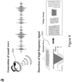
- Fig. 9a shows a schematic representation of a setup for the detection of vibration using a graphene sensor according to an example embodiment. Acoustic wave was utilized to generate dynamic forces with high frequencies.
- Fig. 9b shows a graph illustrating the detection results of dynamic forces with frequencies of 500 Hz, 1000 Hz and 1500 Hz.
- Figs. 9c to 9e shows the Fast Fourier Transform (FFT) of the respective detection results in Fig. 9b , showing the corresponding frequencies 901-903 that the sensor detected.
- FFT Fast Fourier Transform
- the sensor 912 according to an example embodiment was shown to be able to detect the vibration with a high frequency of at least 1500 Hz.
- Fig. 9b gives the detection results of the vibration with frequencies of 500 Hz, 1000 Hz and 1500 Hz.
- FFT fast Fourier transform
- Figs. 9c to 9e illustrate the FFT analysis results of these signals (500 Hz, 1000 Hz and 1500 Hz, respectively).
- a composite structure for a pressure sensor comprising an array of microstructures made from an elastomeric material; and a flexible conductive coating formed on the array of microstructures with a sufficiently thin thickness such that a surface morphology of the array of microstructures is substantially maintained for the coated array of the microstructures; wherein the conductive coating exhibits a Young's modulus that is higher than that of the elastomeric material.
- the Young's modulus may be about one order of magnitude higher than that of the elastomeric material, or more.
- the flexible conductive coating comprises a low dimensional electronically active material system.
- the low dimensional electronically active material system exhibits electron tunneling properties.
- the low dimensional electronically active material system comprises a uniform layer.
- the composite structure may further comprise a substrate for the array of microstructures.
- the composite structure may further comprise an intermediate layer between the array of microstructures and the flexible conductive coating for improved uniformity of the flexible conductive coating.
- a pressure sensor comprising the composite structure of the above embodiment.
- the pressure sensor may exhibit a reduced hysteresis based on elastic properties of the composite structure compared to viscoelastic properties of the elastomeric material of the array of microstructures.
- the pressure sensor may exhibit a substantially frequency independent pressure response.
- the pressure sensor may exhibit a substantially temperature independent pressure response.
- the pressure sensor may exhibit a substantially humidity independent pressure response.
- the pressure sensor may further comprise electrodes disposed on the coated array of microstructures for measuring a resistance of an electric path comprising a portion of a surface of the coated array of microstructures.
- the electrodes may comprise two interdigital electrodes. The resistance may change as a result of compression of the coated array of microstructures under a pressure. The resistance may decrease with increasing pressure.
- Figure 11 shows a flowchart 1100 illustrating a method of fabricating a composite structure for a pressure sensor, according to an example embodiment.
- an array of microstructures made from an elastomeric material is formed.
- a flexible conductive coating is formed on the array of microstructures such that a surface morphology of microstructures is substantially maintained for the coated array of the microstructures, wherein the conductive coating exhibits a Young's modulus that is higher than that of the elastomeric material.
- Forming the flexible coating comprises drop casting a first material onto the array of microstructures.
- the method may comprise blading a second material onto the array of microstructures prior to drop casting the first material.
- the first material comprises a low dimensional electronically active material system.
- the low dimensional electronically active material system exhibits electron tunneling properties.
- the low dimensional electronically active material system may comprise a uniform layer.
- the electronically active material system may comprise 2D material structures.
- the 2D material structures may comprise nanoflakes.
- the method may further comprise disposing electrodes on the coated array of microstructures for measuring a resistance of an electric path comprising a portion of a surface of the coated array of microstructures.
- a method of pressure sensing using the pressor sensor of the above embodiment is provided.
- Embodiments of the present invention can have one or more of the following features and associated benefits/advantages: Feature Benefit/Advantage 1.
- Fast and easy fabrication The fabrication method is fast and easy. Large-scale fabrication of sensor array can be achieved.
- Wide pressure detection range The sensor is able to demonstrate a wide sensitive range of at least 140 kPa. This wide range can satisfy the pressure sensing ability required by fingers.
- Low hysteresis The sensor can identically detect the pressure regardless the loading and unloading process, which improves the accuracy of sensing ability. 4. High reliability and durability The sensor is highly reliable and tested at least 1,000,000 cycles, without inducing a significant change in pressure response and hysteresis. 5.
- the sensor performance is independent of temperature, humidity and strain rate, providing a reliable sensing ability at different ambient conditions.
- the pressure response of the sensor can be tunable by changing the times of coating, as well as the concentration of graphene.
- Detection of small pressure The sensor is capable of detecting small pressures of less than 10 Pa, which is comparable with the sensing ability of fingers.
- Fast response The sensor can detect pressure with a high time resolution. The fast response of sensor can make it detect signals with high frequencies of at least 1500 Hz.
- Embodiments of the present invention can have the following applications, by way of example, not limitation:
- aspects of the systems and methods described herein may be implemented as functionality programmed into any of a variety of circuitry, including programmable logic devices (PLDs), such as field programmable gate arrays (FPGAs), programmable array logic (PAL) devices, electrically programmable logic and memory devices and standard cell-based devices, as well as application specific integrated circuits (ASICs).
- PLDs programmable logic devices
- FPGAs field programmable gate arrays
- PAL programmable array logic
- ASICs application specific integrated circuits
- microcontrollers with memory such as electronically erasable programmable read only memory (EEPROM)
- embedded microprocessors firmware, software, etc.
- aspects of the system may be embodied in microprocessors having software-based circuit emulation, discrete logic (sequential and combinatorial), custom devices, fuzzy (neural) logic, quantum devices, and hybrids of any of the above device types.
- the underlying device technologies may be provided in a variety of component types, e.g., metal-oxide semiconductor field-effect transistor (MOSFET) technologies like complementary metal-oxide semiconductor (CMOS), bipolar technologies like emitter-coupled logic (ECL), polymer technologies (e.g., silicon-conjugated polymer and metal-conjugated polymer-metal structures), mixed analog and digital, etc.
- MOSFET metal-oxide semiconductor field-effect transistor
- CMOS complementary metal-oxide semiconductor
- bipolar technologies like emitter-coupled logic (ECL)
- polymer technologies e.g., silicon-conjugated polymer and metal-conjugated polymer-metal structures
- mixed analog and digital etc.
Landscapes
- Physics & Mathematics (AREA)
- General Physics & Mathematics (AREA)
- Chemical & Material Sciences (AREA)
- Analytical Chemistry (AREA)
- Engineering & Computer Science (AREA)
- Power Engineering (AREA)
- Pressure Sensors (AREA)
Claims (15)
- Eine Verbundstruktur (120) für einen Drucksensor, wobei die Verbundstruktur aufweist:eine Anordnung von Mikrostrukturen (115) aus einem Elastomermaterial;
undeine flexible leitfähige Beschichtung, die auf der Anordnung von Mikrostrukturen mit einer ausreichend geringen Dicke ausgebildet ist, so dass eine Oberflächenmorphologie der Anordnung von Mikrostrukturen für die beschichtete Anordnung der Mikrostrukturen im Wesentlichen erhalten bleibt;wobei die leitfähige Beschichtung ein Elastizitätsmodul aufweist, der höher ist als der des Elastomermaterials; unddadurch gekennzeichnet, dass die flexible leitfähige Beschichtung ein niedrigdimensionales elektronisch aktives Materialsystem aufweist, wobei das niedrigdimensionale elektronisch aktive Materialsystem Elektronentunneleigenschaften aufweist. - Die Verbundstruktur gemäß Anspruch 1, wobei der Elastizitätsmodul etwa eine Größenordnung oder mehr höher ist als der des Elastomermaterials.
- Die Verbundstruktur gemäß Anspruch 1, wobei das niedrigdimensionale elektronisch aktive Materialsystem eine gleichmäßige Schicht aufweist und/oder wobei das niedrigdimensionale elektronisch aktive Materialsystem 2D-Materialstrukturen aufweist, die Nanoflocken aufweisen können.
- Die Verbundstruktur gemäß einem der vorhergehenden Ansprüche, die außerdem ein Substrat für die Anordnung von Mikrostrukturen oder eine Zwischenschicht zwischen der Anordnung von Mikrostrukturen und der flexiblen leitfähigen Beschichtung zur Verbesserung der Gleichmäßigkeit der flexiblen leitfähigen Beschichtung aufweist.
- Ein Drucksensor, der die Verbundstruktur gemäß Anspruch 1 aufweist.
- Der Drucksensor gemäß Anspruch 5, der aufgrund der elastischen Eigenschaften der Verbundstruktur eine geringere Hysterese aufweist im Vergleich zu den viskoelastischen Eigenschaften des Elastomermaterials der Anordnung von Mikrostrukturen.
- Der Drucksensor gemäß Anspruch 5 oder 6, der eine im Wesentlichen frequenzunabhängige Druckreaktion aufweist.
- Der Drucksensor gemäß einem der Ansprüche 5 bis 7, der eine im Wesentlichen temperaturunabhängige Druckreaktion und/oder eine im Wesentlichen feuchtigkeitsunabhängige Druckreaktion aufweist.
- Der Drucksensor gemäß einem der Ansprüche 5 bis 8, der außerdem Elektroden (116, 118) aufweist, die auf der beschichteten Anordnung von Mikrostrukturen angeordnet sind, um einen Widerstand eines elektrischen Pfads zu messen, der einen Teil einer Oberfläche der beschichteten Anordnung von Mikrostrukturen aufweist, und wobei die Elektroden optional zwei Interdigitalelektroden aufweisen, die zwei Interdigitalelektroden aufweisen können.
- Der Drucksensor gemäß Anspruch 9, wobei sich der Widerstand infolge der Kompression der beschichteten Anordnung von Mikrostrukturen unter Druck ändert und wobei der Widerstand optional mit zunehmendem Druck abnimmt.
- Ein Verfahren zur Herstellung einer Verbundstruktur (120) für einen Drucksensor, wobei das Verfahren die Schritte aufweist:Bilden einer Anordnung von Mikrostrukturen (115) aus einem Elastomermaterial; undBilden einer flexiblen leitfähigen Beschichtung auf der Anordnung von Mikrostrukturen, so dass eine Oberflächenmorphologie der Mikrostrukturen für die beschichtete Anordnung der Mikrostrukturen im Wesentlichen erhalten bleibt;wobei die leitfähige Beschichtung ein Elastizitätsmodul aufweist, der höher ist als der des Elastomermaterials;dadurch gekennzeichnet, dass das Verfahren den Schritt des Bildens der flexiblen Beschichtung aufweist, bei dem ein erstes Material durch Tropfengießen auf die Anordnung von Mikrostrukturen aufgebracht wird; undwobei das erste Material ein niedrigdimensionales elektronisch aktives Materialsystem aufweist, wobei das niedrigdimensionale elektronisch aktive Materialsystem Elektronentunneleigenschaften aufweist.
- Das Verfahren gemäß Anspruch 11, aufweisend das Aufbringen eines zweiten Materials auf die Anordnung von Mikrostrukturen vor dem Tropfengießen des ersten Materials.
- Das Verfahren gemäß den Ansprüchen 11 oder 12, wobei das niedrigdimensionale elektronisch aktive Materialsystem eine gleichmäßige Schicht aufweist und/oder wobei das elektronisch aktive Materialsystem optional 2D-Materialstrukturen aufweist, die Nanoflocken aufweisen können.
- Das Verfahren gemäß einem der Ansprüche 11 bis 13, das außerdem das Anordnen von Elektroden auf der beschichteten Anordnung von Mikrostrukturen zum Messen eines Widerstands eines elektrischen Pfads aufweist, der einen Teil einer Oberfläche der beschichteten Anordnung von Mikrostrukturen aufweist.
- Ein Verfahren zur Druckmessung unter Verwendung des Drucksensors gemäß einem der Ansprüche 5 bis 10.
Applications Claiming Priority (2)
| Application Number | Priority Date | Filing Date | Title |
|---|---|---|---|
| SG10201905267P | 2019-06-10 | ||
| PCT/SG2020/050325 WO2020251473A1 (en) | 2019-06-10 | 2020-06-10 | Composite structure for a pressure sensor and pressure sensor |
Publications (3)
| Publication Number | Publication Date |
|---|---|
| EP3980740A1 EP3980740A1 (de) | 2022-04-13 |
| EP3980740A4 EP3980740A4 (de) | 2022-08-10 |
| EP3980740B1 true EP3980740B1 (de) | 2025-04-23 |
Family
ID=73782270
Family Applications (1)
| Application Number | Title | Priority Date | Filing Date |
|---|---|---|---|
| EP20822209.1A Active EP3980740B1 (de) | 2019-06-10 | 2020-06-10 | Verbundstruktur für einen drucksensor und drucksensor |
Country Status (4)
| Country | Link |
|---|---|
| US (1) | US12392673B2 (de) |
| EP (1) | EP3980740B1 (de) |
| JP (1) | JP7663516B2 (de) |
| WO (1) | WO2020251473A1 (de) |
Families Citing this family (14)
| Publication number | Priority date | Publication date | Assignee | Title |
|---|---|---|---|---|
| CN210864624U (zh) * | 2020-01-22 | 2020-06-26 | 湃瑞电子科技(苏州)有限公司 | 压力传感器及电子设备 |
| EP4019926A1 (de) * | 2020-12-22 | 2022-06-29 | Max-Planck-Gesellschaft zur Förderung der Wissenschaften e.V. | System und verfahren zur gleichzeitigen erfassung von kontaktkraft und seitlicher belastung |
| WO2022250939A1 (en) * | 2021-05-27 | 2022-12-01 | The University Of Chicago | Strain-insensitive soft pressure sensor and method of measuring pressure |
| CN114046913A (zh) * | 2021-11-17 | 2022-02-15 | 燕山大学 | 一种柔性石墨烯压力传感器及其制备方法 |
| WO2023159498A1 (zh) * | 2022-02-25 | 2023-08-31 | 京东方科技集团股份有限公司 | 显示面板及其制备方法、显示装置 |
| CN115290229B (zh) * | 2022-08-02 | 2025-02-07 | 杭州电子科技大学 | 一种石墨烯基高灵敏柔性多功能传感器及其制备方法 |
| CN115655528B (zh) * | 2022-10-18 | 2025-09-02 | 中国科学院重庆绿色智能技术研究院 | 基于二维量子隧穿力敏机制的柔性压力传感器及制备方法 |
| CN115805375B (zh) * | 2022-11-22 | 2024-07-30 | 厦门大学 | 一种互锁一体化微结构的压力传感器及其制造方法 |
| CN115901034A (zh) * | 2022-12-14 | 2023-04-04 | 中国科学院苏州纳米技术与纳米仿生研究所 | 一种可识别物体软硬的柔性压阻传感器及其制备方法和应用 |
| CN115855324B (zh) * | 2022-12-26 | 2024-04-30 | 厦门大学 | 一种检测锂电池电芯膨胀的薄膜压力传感器及其制备方法 |
| CN116223852A (zh) * | 2023-03-18 | 2023-06-06 | 北京理工大学 | 一种相结构调控二维铁磁材料弹性性能的方法 |
| CN116945793A (zh) * | 2023-07-11 | 2023-10-27 | 中央民族大学 | 石墨烯-铜复合柔性电子皮肤及其制备方法和电子纹身的应用 |
| CN118945987B (zh) * | 2024-07-24 | 2025-09-19 | 中国海洋大学 | 基于丝网印刷的最小端口叉指传感器阵列及其制备方法 |
| CN119666072B (zh) * | 2024-12-12 | 2025-09-26 | 郑州大学 | 一种柔性压力-温度双模态传感器 |
Family Cites Families (26)
| Publication number | Priority date | Publication date | Assignee | Title |
|---|---|---|---|---|
| WO2008143012A1 (ja) * | 2007-05-11 | 2008-11-27 | Bridgestone Corporation | 導電性ローラ及び導電性ローラの製造方法 |
| CN104039695B (zh) | 2011-09-19 | 2018-06-05 | 卧龙岗大学 | 还原氧化石墨烯及其生产方法 |
| US20140370246A1 (en) * | 2012-01-20 | 2014-12-18 | Brown University | Substrate with Graphene-based Layer |
| US11850052B2 (en) * | 2014-01-28 | 2023-12-26 | Medibotics Llc | Dry EEG electrode for use on a hair-covered portion of a person's head |
| KR102081892B1 (ko) * | 2013-09-05 | 2020-02-26 | 삼성전자주식회사 | 압저항(piezo-resistive) 전극을 구비한 저항성 압력 센서 |
| CN104257367B (zh) | 2014-09-16 | 2016-04-06 | 苏州能斯达电子科技有限公司 | 一种可贴附柔性压力传感器及其制备方法 |
| CN104949779B (zh) * | 2015-07-21 | 2017-09-08 | 中国科学技术大学 | 一种压力传感器及其制备方法 |
| CN105067160B (zh) | 2015-07-23 | 2017-10-03 | 东南大学 | 基于氧化石墨烯海绵的柔性压力传感器 |
| CN109104877A (zh) | 2016-02-03 | 2018-12-28 | 畅想智能材料有限公司 | 具有导电性能的土工织品 |
| CN106017751B (zh) * | 2016-05-25 | 2018-08-10 | 东南大学 | 一种高灵敏度压阻式压力传感器及其制备方法 |
| KR101987363B1 (ko) | 2016-09-30 | 2019-06-11 | 한국과학기술연구원 | 비연속적 전도성 패턴을 포함하는 압력 센서, 이를 포함하는 디바이스, 및 압력을 감지하는 장치 및 방법 |
| KR101902790B1 (ko) | 2016-10-31 | 2018-10-01 | 재단법인 나노기반소프트일렉트로닉스연구단 | 고분자층/전도층을 포함하는 적층체, 그를 포함하는 고민감성 및 선형 민감성을 갖는 압력 센서, 및 그의 제조 방법 |
| CN106595916A (zh) | 2016-12-02 | 2017-04-26 | 华东师范大学 | 一种碳基电阻式柔性压力传感器 |
| WO2018144772A1 (en) | 2017-02-03 | 2018-08-09 | The Regents Of The University Of California | Enhanced pressure sensing performance for pressure sensors |
| GB201702724D0 (en) * | 2017-02-20 | 2017-04-05 | Univ Court Univ Of Glasgow | Sensor and devices incorporating sensors |
| KR101982177B1 (ko) * | 2017-07-25 | 2019-05-24 | 포항공과대학교 산학협력단 | 압력센서, 그를 포함하는 압력센서 매트릭스 어레이 및 그의 제조방법 |
| US10825586B2 (en) * | 2017-08-30 | 2020-11-03 | Ultra Conductive Copper Company, Inc. | Method and system for forming a multilayer composite structure |
| CN108007617A (zh) * | 2017-12-05 | 2018-05-08 | 浙江大学 | 具有微圆锥台基底的压阻式柔性触觉传感器及其制造方法 |
| CN108332887B (zh) | 2018-04-28 | 2024-08-23 | 河北工业大学 | 一种柔性应力传感器 |
| CN108896215B (zh) * | 2018-05-21 | 2020-11-06 | 福建师范大学 | 压力传感器制备方法及其制备的压力传感器 |
| CN108975266B (zh) * | 2018-07-17 | 2020-11-10 | 中北大学 | 基于针尖阵列结构的石墨烯-pdms柔性衬底心电干电极及其制备方法 |
| CN108871629A (zh) | 2018-07-20 | 2018-11-23 | 浙江大学 | 一种柔性电阻式压力传感器阵列及其制备方法 |
| CN109186817B (zh) | 2018-09-13 | 2022-10-11 | 深圳光韵达机电设备有限公司 | 一种电容式柔性压力传感器及其制造方法 |
| CA3051372A1 (en) * | 2018-11-14 | 2020-05-14 | University Of Windsor | Method of fabricating flexible pressure sensor |
| WO2020162836A1 (en) * | 2019-02-08 | 2020-08-13 | National University Of Singapore | Low hysteresis and flexible pressure sensitive composite |
| WO2020214808A1 (en) * | 2019-04-17 | 2020-10-22 | The Regents Of The University Of California | Scalable and high-performance pressure sensors for wearable electronics |
-
2020
- 2020-06-10 EP EP20822209.1A patent/EP3980740B1/de active Active
- 2020-06-10 JP JP2021573505A patent/JP7663516B2/ja active Active
- 2020-06-10 US US17/618,258 patent/US12392673B2/en active Active
- 2020-06-10 WO PCT/SG2020/050325 patent/WO2020251473A1/en not_active Ceased
Also Published As
| Publication number | Publication date |
|---|---|
| US12392673B2 (en) | 2025-08-19 |
| JP2022536357A (ja) | 2022-08-15 |
| EP3980740A4 (de) | 2022-08-10 |
| US20220299385A1 (en) | 2022-09-22 |
| JP7663516B2 (ja) | 2025-04-16 |
| EP3980740A1 (de) | 2022-04-13 |
| WO2020251473A1 (en) | 2020-12-17 |
Similar Documents
| Publication | Publication Date | Title |
|---|---|---|
| EP3980740B1 (de) | Verbundstruktur für einen drucksensor und drucksensor | |
| Zhang et al. | Simple and efficient pressure sensor based on PDMS wrapped CNT arrays | |
| JP6049898B2 (ja) | 圧力感知装置及びその組立方法 | |
| Gong et al. | Local crack‐programmed gold nanowire electronic skin tattoos for in‐plane multisensor integration | |
| Ma et al. | A highly sensitive and flexible capacitive pressure sensor based on a micro-arrayed polydimethylsiloxane dielectric layer | |
| Gong et al. | A location-and sharpness-specific tactile electronic skin based on staircase-like nanowire patches | |
| EP3921616B1 (de) | Hysteresearmer und flexibler druckempfindlicher verbundstoff | |
| Chen et al. | Flexible capacitive pressure sensor based on multi-walled carbon nanotubes microstructure electrodes | |
| US20140037909A1 (en) | Actuation and Control of Stamp Deformation in Microcontact Printing | |
| US10138542B2 (en) | Mechanically gated electrical switches by creasing of patterned metal/elastomer bilayer films | |
| Gu et al. | Flexible electronic eardrum | |
| CN108291797A (zh) | 含直线诱导的裂纹的高灵敏度传感器及其制造方法 | |
| Zhang et al. | Continuous graphene and carbon nanotube based high flexible and transparent pressure sensor arrays | |
| KR20180097969A (ko) | 크랙 치유 고분자를 포함하는 크랙 센서 및 이를 포함하는 전자 소자 | |
| Guo et al. | Pre-fatigue enhancing both long-term stability and sensitivity of direct-ink-writing printed sensors | |
| Chen et al. | Improving the sensitivity of elastic capacitive pressure sensors using silver nanowire mesh electrodes | |
| CN107748024A (zh) | 一种微图案化的柔性触觉传感器及其制备方法 | |
| Su et al. | Tunable flexible pressure sensor based on bioinspired capillary-driven method | |
| van Dommelen et al. | Fully 3d printed mechanical pressure sensors: a comparison of sensing mechanisms | |
| Ventrelli et al. | Development of a stretchable skin-like tactile sensor based on polymeric composites | |
| Choi et al. | Spatially digitized tactile pressure sensors with tunable sensitivity and sensing range | |
| US11119064B2 (en) | Cell-on-chip stretchable platform for mammalian cells with integrated impedance spectroscpy technique | |
| Lu et al. | Fabrication technology of piezoresistive conductive PDMS for micro fingerprint sensors | |
| US20220291060A1 (en) | Elastomeric Sensor | |
| Tuinea-Bobe et al. | Photolithographic structuring of stretchable conductors and sub-kPa pressure sensors |
Legal Events
| Date | Code | Title | Description |
|---|---|---|---|
| STAA | Information on the status of an ep patent application or granted ep patent |
Free format text: STATUS: THE INTERNATIONAL PUBLICATION HAS BEEN MADE |
|
| PUAI | Public reference made under article 153(3) epc to a published international application that has entered the european phase |
Free format text: ORIGINAL CODE: 0009012 |
|
| STAA | Information on the status of an ep patent application or granted ep patent |
Free format text: STATUS: REQUEST FOR EXAMINATION WAS MADE |
|
| 17P | Request for examination filed |
Effective date: 20211220 |
|
| AK | Designated contracting states |
Kind code of ref document: A1 Designated state(s): AL AT BE BG CH CY CZ DE DK EE ES FI FR GB GR HR HU IE IS IT LI LT LU LV MC MK MT NL NO PL PT RO RS SE SI SK SM TR |
|
| A4 | Supplementary search report drawn up and despatched |
Effective date: 20220712 |
|
| RIC1 | Information provided on ipc code assigned before grant |
Ipc: B32B 3/30 20060101ALI20220706BHEP Ipc: G01L 1/20 20060101AFI20220706BHEP |
|
| DAV | Request for validation of the european patent (deleted) | ||
| DAX | Request for extension of the european patent (deleted) | ||
| GRAP | Despatch of communication of intention to grant a patent |
Free format text: ORIGINAL CODE: EPIDOSNIGR1 |
|
| STAA | Information on the status of an ep patent application or granted ep patent |
Free format text: STATUS: GRANT OF PATENT IS INTENDED |
|
| INTG | Intention to grant announced |
Effective date: 20241114 |
|
| GRAS | Grant fee paid |
Free format text: ORIGINAL CODE: EPIDOSNIGR3 |
|
| GRAA | (expected) grant |
Free format text: ORIGINAL CODE: 0009210 |
|
| STAA | Information on the status of an ep patent application or granted ep patent |
Free format text: STATUS: THE PATENT HAS BEEN GRANTED |
|
| AK | Designated contracting states |
Kind code of ref document: B1 Designated state(s): AL AT BE BG CH CY CZ DE DK EE ES FI FR GB GR HR HU IE IS IT LI LT LU LV MC MK MT NL NO PL PT RO RS SE SI SK SM TR |
|
| REG | Reference to a national code |
Ref country code: GB Ref legal event code: FG4D |
|
| REG | Reference to a national code |
Ref country code: CH Ref legal event code: EP |
|
| P01 | Opt-out of the competence of the unified patent court (upc) registered |
Free format text: CASE NUMBER: APP_15374/2025 Effective date: 20250328 |
|
| REG | Reference to a national code |
Ref country code: DE Ref legal event code: R096 Ref document number: 602020050077 Country of ref document: DE |
|
| REG | Reference to a national code |
Ref country code: IE Ref legal event code: FG4D |
|
| PGFP | Annual fee paid to national office [announced via postgrant information from national office to epo] |
Ref country code: DE Payment date: 20250617 Year of fee payment: 6 |
|
| PGFP | Annual fee paid to national office [announced via postgrant information from national office to epo] |
Ref country code: GB Payment date: 20250625 Year of fee payment: 6 |
|
| REG | Reference to a national code |
Ref country code: NL Ref legal event code: MP Effective date: 20250423 |
|
| PG25 | Lapsed in a contracting state [announced via postgrant information from national office to epo] |
Ref country code: NL Free format text: LAPSE BECAUSE OF FAILURE TO SUBMIT A TRANSLATION OF THE DESCRIPTION OR TO PAY THE FEE WITHIN THE PRESCRIBED TIME-LIMIT Effective date: 20250423 |
|
| REG | Reference to a national code |
Ref country code: AT Ref legal event code: MK05 Ref document number: 1788157 Country of ref document: AT Kind code of ref document: T Effective date: 20250423 |
|
| PG25 | Lapsed in a contracting state [announced via postgrant information from national office to epo] |
Ref country code: FI Free format text: LAPSE BECAUSE OF FAILURE TO SUBMIT A TRANSLATION OF THE DESCRIPTION OR TO PAY THE FEE WITHIN THE PRESCRIBED TIME-LIMIT Effective date: 20250423 Ref country code: ES Free format text: LAPSE BECAUSE OF FAILURE TO SUBMIT A TRANSLATION OF THE DESCRIPTION OR TO PAY THE FEE WITHIN THE PRESCRIBED TIME-LIMIT Effective date: 20250423 Ref country code: PT Free format text: LAPSE BECAUSE OF FAILURE TO SUBMIT A TRANSLATION OF THE DESCRIPTION OR TO PAY THE FEE WITHIN THE PRESCRIBED TIME-LIMIT Effective date: 20250825 |
|
| REG | Reference to a national code |
Ref country code: LT Ref legal event code: MG9D |
|
| PG25 | Lapsed in a contracting state [announced via postgrant information from national office to epo] |
Ref country code: GR Free format text: LAPSE BECAUSE OF FAILURE TO SUBMIT A TRANSLATION OF THE DESCRIPTION OR TO PAY THE FEE WITHIN THE PRESCRIBED TIME-LIMIT Effective date: 20250724 Ref country code: NO Free format text: LAPSE BECAUSE OF FAILURE TO SUBMIT A TRANSLATION OF THE DESCRIPTION OR TO PAY THE FEE WITHIN THE PRESCRIBED TIME-LIMIT Effective date: 20250723 |
|
| PG25 | Lapsed in a contracting state [announced via postgrant information from national office to epo] |
Ref country code: PL Free format text: LAPSE BECAUSE OF FAILURE TO SUBMIT A TRANSLATION OF THE DESCRIPTION OR TO PAY THE FEE WITHIN THE PRESCRIBED TIME-LIMIT Effective date: 20250423 |
|
| PG25 | Lapsed in a contracting state [announced via postgrant information from national office to epo] |
Ref country code: BG Free format text: LAPSE BECAUSE OF FAILURE TO SUBMIT A TRANSLATION OF THE DESCRIPTION OR TO PAY THE FEE WITHIN THE PRESCRIBED TIME-LIMIT Effective date: 20250423 |
|
| PG25 | Lapsed in a contracting state [announced via postgrant information from national office to epo] |
Ref country code: HR Free format text: LAPSE BECAUSE OF FAILURE TO SUBMIT A TRANSLATION OF THE DESCRIPTION OR TO PAY THE FEE WITHIN THE PRESCRIBED TIME-LIMIT Effective date: 20250423 |
|
| PG25 | Lapsed in a contracting state [announced via postgrant information from national office to epo] |
Ref country code: AT Free format text: LAPSE BECAUSE OF FAILURE TO SUBMIT A TRANSLATION OF THE DESCRIPTION OR TO PAY THE FEE WITHIN THE PRESCRIBED TIME-LIMIT Effective date: 20250423 |
|
| PG25 | Lapsed in a contracting state [announced via postgrant information from national office to epo] |
Ref country code: RS Free format text: LAPSE BECAUSE OF FAILURE TO SUBMIT A TRANSLATION OF THE DESCRIPTION OR TO PAY THE FEE WITHIN THE PRESCRIBED TIME-LIMIT Effective date: 20250723 |
|
| PG25 | Lapsed in a contracting state [announced via postgrant information from national office to epo] |
Ref country code: IS Free format text: LAPSE BECAUSE OF FAILURE TO SUBMIT A TRANSLATION OF THE DESCRIPTION OR TO PAY THE FEE WITHIN THE PRESCRIBED TIME-LIMIT Effective date: 20250823 |
|
| PG25 | Lapsed in a contracting state [announced via postgrant information from national office to epo] |
Ref country code: LV Free format text: LAPSE BECAUSE OF FAILURE TO SUBMIT A TRANSLATION OF THE DESCRIPTION OR TO PAY THE FEE WITHIN THE PRESCRIBED TIME-LIMIT Effective date: 20250423 |
|
| PG25 | Lapsed in a contracting state [announced via postgrant information from national office to epo] |
Ref country code: SM Free format text: LAPSE BECAUSE OF FAILURE TO SUBMIT A TRANSLATION OF THE DESCRIPTION OR TO PAY THE FEE WITHIN THE PRESCRIBED TIME-LIMIT Effective date: 20250423 Ref country code: DK Free format text: LAPSE BECAUSE OF FAILURE TO SUBMIT A TRANSLATION OF THE DESCRIPTION OR TO PAY THE FEE WITHIN THE PRESCRIBED TIME-LIMIT Effective date: 20250423 |
|
| PG25 | Lapsed in a contracting state [announced via postgrant information from national office to epo] |
Ref country code: CZ Free format text: LAPSE BECAUSE OF FAILURE TO SUBMIT A TRANSLATION OF THE DESCRIPTION OR TO PAY THE FEE WITHIN THE PRESCRIBED TIME-LIMIT Effective date: 20250423 |
|
| PG25 | Lapsed in a contracting state [announced via postgrant information from national office to epo] |
Ref country code: EE Free format text: LAPSE BECAUSE OF FAILURE TO SUBMIT A TRANSLATION OF THE DESCRIPTION OR TO PAY THE FEE WITHIN THE PRESCRIBED TIME-LIMIT Effective date: 20250423 |
|
| REG | Reference to a national code |
Ref country code: DE Ref legal event code: R097 Ref document number: 602020050077 Country of ref document: DE |
|
| PG25 | Lapsed in a contracting state [announced via postgrant information from national office to epo] |
Ref country code: SK Free format text: LAPSE BECAUSE OF FAILURE TO SUBMIT A TRANSLATION OF THE DESCRIPTION OR TO PAY THE FEE WITHIN THE PRESCRIBED TIME-LIMIT Effective date: 20250423 Ref country code: RO Free format text: LAPSE BECAUSE OF FAILURE TO SUBMIT A TRANSLATION OF THE DESCRIPTION OR TO PAY THE FEE WITHIN THE PRESCRIBED TIME-LIMIT Effective date: 20250423 |
|
| REG | Reference to a national code |
Ref country code: CH Ref legal event code: H13 Free format text: ST27 STATUS EVENT CODE: U-0-0-H10-H13 (AS PROVIDED BY THE NATIONAL OFFICE) Effective date: 20260127 |
|
| PG25 | Lapsed in a contracting state [announced via postgrant information from national office to epo] |
Ref country code: IT Free format text: LAPSE BECAUSE OF FAILURE TO SUBMIT A TRANSLATION OF THE DESCRIPTION OR TO PAY THE FEE WITHIN THE PRESCRIBED TIME-LIMIT Effective date: 20250423 |
|
| PG25 | Lapsed in a contracting state [announced via postgrant information from national office to epo] |
Ref country code: MC Free format text: LAPSE BECAUSE OF FAILURE TO SUBMIT A TRANSLATION OF THE DESCRIPTION OR TO PAY THE FEE WITHIN THE PRESCRIBED TIME-LIMIT Effective date: 20250423 |
|
| PG25 | Lapsed in a contracting state [announced via postgrant information from national office to epo] |
Ref country code: LU Free format text: LAPSE BECAUSE OF NON-PAYMENT OF DUE FEES Effective date: 20250610 |
|
| REG | Reference to a national code |
Ref country code: BE Ref legal event code: MM Effective date: 20250630 |
|
| PLBE | No opposition filed within time limit |
Free format text: ORIGINAL CODE: 0009261 |
|
| STAA | Information on the status of an ep patent application or granted ep patent |
Free format text: STATUS: NO OPPOSITION FILED WITHIN TIME LIMIT |
|
| REG | Reference to a national code |
Ref country code: CH Ref legal event code: L10 Free format text: ST27 STATUS EVENT CODE: U-0-0-L10-L00 (AS PROVIDED BY THE NATIONAL OFFICE) Effective date: 20260304 |