EP3979485A1 - Power conversion device - Google Patents
Power conversion device Download PDFInfo
- Publication number
- EP3979485A1 EP3979485A1 EP20818334.3A EP20818334A EP3979485A1 EP 3979485 A1 EP3979485 A1 EP 3979485A1 EP 20818334 A EP20818334 A EP 20818334A EP 3979485 A1 EP3979485 A1 EP 3979485A1
- Authority
- EP
- European Patent Office
- Prior art keywords
- period
- phase
- switching element
- carrier cycle
- voltage command
- Prior art date
- Legal status (The legal status is an assumption and is not a legal conclusion. Google has not performed a legal analysis and makes no representation as to the accuracy of the status listed.)
- Pending
Links
- 238000006243 chemical reaction Methods 0.000 title claims abstract description 45
- 238000005192 partition Methods 0.000 description 18
- 230000006835 compression Effects 0.000 description 15
- 238000007906 compression Methods 0.000 description 15
- 239000003507 refrigerant Substances 0.000 description 9
- 239000000758 substrate Substances 0.000 description 8
- 238000010586 diagram Methods 0.000 description 7
- 238000000034 method Methods 0.000 description 6
- 238000001514 detection method Methods 0.000 description 4
- 239000003990 capacitor Substances 0.000 description 3
- 230000007423 decrease Effects 0.000 description 3
- 238000009499 grossing Methods 0.000 description 3
- 230000020169 heat generation Effects 0.000 description 3
- 230000006866 deterioration Effects 0.000 description 2
- 238000010606 normalization Methods 0.000 description 2
- 238000004378 air conditioning Methods 0.000 description 1
- 239000004020 conductor Substances 0.000 description 1
- 230000003247 decreasing effect Effects 0.000 description 1
- 230000000694 effects Effects 0.000 description 1
- 239000012530 fluid Substances 0.000 description 1
- WABPQHHGFIMREM-UHFFFAOYSA-N lead(0) Chemical compound [Pb] WABPQHHGFIMREM-UHFFFAOYSA-N 0.000 description 1
- 230000007935 neutral effect Effects 0.000 description 1
- 230000000149 penetrating effect Effects 0.000 description 1
- 238000007789 sealing Methods 0.000 description 1
- 230000001360 synchronised effect Effects 0.000 description 1
Images



Classifications
-
- H—ELECTRICITY
- H02—GENERATION; CONVERSION OR DISTRIBUTION OF ELECTRIC POWER
- H02M—APPARATUS FOR CONVERSION BETWEEN AC AND AC, BETWEEN AC AND DC, OR BETWEEN DC AND DC, AND FOR USE WITH MAINS OR SIMILAR POWER SUPPLY SYSTEMS; CONVERSION OF DC OR AC INPUT POWER INTO SURGE OUTPUT POWER; CONTROL OR REGULATION THEREOF
- H02M7/00—Conversion of AC power input into DC power output; Conversion of DC power input into AC power output
- H02M7/42—Conversion of DC power input into AC power output without possibility of reversal
- H02M7/44—Conversion of DC power input into AC power output without possibility of reversal by static converters
- H02M7/48—Conversion of DC power input into AC power output without possibility of reversal by static converters using discharge tubes with control electrode or semiconductor devices with control electrode
- H02M7/53—Conversion of DC power input into AC power output without possibility of reversal by static converters using discharge tubes with control electrode or semiconductor devices with control electrode using devices of a triode or transistor type requiring continuous application of a control signal
- H02M7/537—Conversion of DC power input into AC power output without possibility of reversal by static converters using discharge tubes with control electrode or semiconductor devices with control electrode using devices of a triode or transistor type requiring continuous application of a control signal using semiconductor devices only, e.g. single switched pulse inverters
- H02M7/539—Conversion of DC power input into AC power output without possibility of reversal by static converters using discharge tubes with control electrode or semiconductor devices with control electrode using devices of a triode or transistor type requiring continuous application of a control signal using semiconductor devices only, e.g. single switched pulse inverters with automatic control of output wave form or frequency
- H02M7/5395—Conversion of DC power input into AC power output without possibility of reversal by static converters using discharge tubes with control electrode or semiconductor devices with control electrode using devices of a triode or transistor type requiring continuous application of a control signal using semiconductor devices only, e.g. single switched pulse inverters with automatic control of output wave form or frequency by pulse-width modulation
-
- H—ELECTRICITY
- H02—GENERATION; CONVERSION OR DISTRIBUTION OF ELECTRIC POWER
- H02P—CONTROL OR REGULATION OF ELECTRIC MOTORS, ELECTRIC GENERATORS OR DYNAMO-ELECTRIC CONVERTERS; CONTROLLING TRANSFORMERS, REACTORS OR CHOKE COILS
- H02P27/00—Arrangements or methods for the control of AC motors characterised by the kind of supply voltage
- H02P27/04—Arrangements or methods for the control of AC motors characterised by the kind of supply voltage using variable-frequency supply voltage, e.g. inverter or converter supply voltage
- H02P27/06—Arrangements or methods for the control of AC motors characterised by the kind of supply voltage using variable-frequency supply voltage, e.g. inverter or converter supply voltage using DC to AC converters or inverters
- H02P27/08—Arrangements or methods for the control of AC motors characterised by the kind of supply voltage using variable-frequency supply voltage, e.g. inverter or converter supply voltage using DC to AC converters or inverters with pulse width modulation
-
- H—ELECTRICITY
- H02—GENERATION; CONVERSION OR DISTRIBUTION OF ELECTRIC POWER
- H02M—APPARATUS FOR CONVERSION BETWEEN AC AND AC, BETWEEN AC AND DC, OR BETWEEN DC AND DC, AND FOR USE WITH MAINS OR SIMILAR POWER SUPPLY SYSTEMS; CONVERSION OF DC OR AC INPUT POWER INTO SURGE OUTPUT POWER; CONTROL OR REGULATION THEREOF
- H02M1/00—Details of apparatus for conversion
- H02M1/0003—Details of control, feedback or regulation circuits
- H02M1/0009—Devices or circuits for detecting current in a converter
-
- H—ELECTRICITY
- H02—GENERATION; CONVERSION OR DISTRIBUTION OF ELECTRIC POWER
- H02M—APPARATUS FOR CONVERSION BETWEEN AC AND AC, BETWEEN AC AND DC, OR BETWEEN DC AND DC, AND FOR USE WITH MAINS OR SIMILAR POWER SUPPLY SYSTEMS; CONVERSION OF DC OR AC INPUT POWER INTO SURGE OUTPUT POWER; CONTROL OR REGULATION THEREOF
- H02M1/00—Details of apparatus for conversion
- H02M1/0048—Circuits or arrangements for reducing losses
- H02M1/0054—Transistor switching losses
-
- H—ELECTRICITY
- H02—GENERATION; CONVERSION OR DISTRIBUTION OF ELECTRIC POWER
- H02M—APPARATUS FOR CONVERSION BETWEEN AC AND AC, BETWEEN AC AND DC, OR BETWEEN DC AND DC, AND FOR USE WITH MAINS OR SIMILAR POWER SUPPLY SYSTEMS; CONVERSION OF DC OR AC INPUT POWER INTO SURGE OUTPUT POWER; CONTROL OR REGULATION THEREOF
- H02M1/00—Details of apparatus for conversion
- H02M1/08—Circuits specially adapted for the generation of control voltages for semiconductor devices incorporated in static converters
- H02M1/088—Circuits specially adapted for the generation of control voltages for semiconductor devices incorporated in static converters for the simultaneous control of series or parallel connected semiconductor devices
-
- H—ELECTRICITY
- H02—GENERATION; CONVERSION OR DISTRIBUTION OF ELECTRIC POWER
- H02M—APPARATUS FOR CONVERSION BETWEEN AC AND AC, BETWEEN AC AND DC, OR BETWEEN DC AND DC, AND FOR USE WITH MAINS OR SIMILAR POWER SUPPLY SYSTEMS; CONVERSION OF DC OR AC INPUT POWER INTO SURGE OUTPUT POWER; CONTROL OR REGULATION THEREOF
- H02M7/00—Conversion of AC power input into DC power output; Conversion of DC power input into AC power output
- H02M7/003—Constructional details, e.g. physical layout, assembly, wiring or busbar connections
-
- H—ELECTRICITY
- H02—GENERATION; CONVERSION OR DISTRIBUTION OF ELECTRIC POWER
- H02M—APPARATUS FOR CONVERSION BETWEEN AC AND AC, BETWEEN AC AND DC, OR BETWEEN DC AND DC, AND FOR USE WITH MAINS OR SIMILAR POWER SUPPLY SYSTEMS; CONVERSION OF DC OR AC INPUT POWER INTO SURGE OUTPUT POWER; CONTROL OR REGULATION THEREOF
- H02M7/00—Conversion of AC power input into DC power output; Conversion of DC power input into AC power output
- H02M7/42—Conversion of DC power input into AC power output without possibility of reversal
- H02M7/44—Conversion of DC power input into AC power output without possibility of reversal by static converters
- H02M7/48—Conversion of DC power input into AC power output without possibility of reversal by static converters using discharge tubes with control electrode or semiconductor devices with control electrode
- H02M7/53—Conversion of DC power input into AC power output without possibility of reversal by static converters using discharge tubes with control electrode or semiconductor devices with control electrode using devices of a triode or transistor type requiring continuous application of a control signal
- H02M7/537—Conversion of DC power input into AC power output without possibility of reversal by static converters using discharge tubes with control electrode or semiconductor devices with control electrode using devices of a triode or transistor type requiring continuous application of a control signal using semiconductor devices only, e.g. single switched pulse inverters
- H02M7/5387—Conversion of DC power input into AC power output without possibility of reversal by static converters using discharge tubes with control electrode or semiconductor devices with control electrode using devices of a triode or transistor type requiring continuous application of a control signal using semiconductor devices only, e.g. single switched pulse inverters in a bridge configuration
- H02M7/53871—Conversion of DC power input into AC power output without possibility of reversal by static converters using discharge tubes with control electrode or semiconductor devices with control electrode using devices of a triode or transistor type requiring continuous application of a control signal using semiconductor devices only, e.g. single switched pulse inverters in a bridge configuration with automatic control of output voltage or current
-
- H—ELECTRICITY
- H02—GENERATION; CONVERSION OR DISTRIBUTION OF ELECTRIC POWER
- H02P—CONTROL OR REGULATION OF ELECTRIC MOTORS, ELECTRIC GENERATORS OR DYNAMO-ELECTRIC CONVERTERS; CONTROLLING TRANSFORMERS, REACTORS OR CHOKE COILS
- H02P27/00—Arrangements or methods for the control of AC motors characterised by the kind of supply voltage
- H02P27/04—Arrangements or methods for the control of AC motors characterised by the kind of supply voltage using variable-frequency supply voltage, e.g. inverter or converter supply voltage
- H02P27/06—Arrangements or methods for the control of AC motors characterised by the kind of supply voltage using variable-frequency supply voltage, e.g. inverter or converter supply voltage using DC to AC converters or inverters
- H02P27/08—Arrangements or methods for the control of AC motors characterised by the kind of supply voltage using variable-frequency supply voltage, e.g. inverter or converter supply voltage using DC to AC converters or inverters with pulse width modulation
- H02P27/085—Arrangements or methods for the control of AC motors characterised by the kind of supply voltage using variable-frequency supply voltage, e.g. inverter or converter supply voltage using DC to AC converters or inverters with pulse width modulation wherein the PWM mode is adapted on the running conditions of the motor, e.g. the switching frequency
-
- H—ELECTRICITY
- H02—GENERATION; CONVERSION OR DISTRIBUTION OF ELECTRIC POWER
- H02P—CONTROL OR REGULATION OF ELECTRIC MOTORS, ELECTRIC GENERATORS OR DYNAMO-ELECTRIC CONVERTERS; CONTROLLING TRANSFORMERS, REACTORS OR CHOKE COILS
- H02P6/00—Arrangements for controlling synchronous motors or other dynamo-electric motors using electronic commutation dependent on the rotor position; Electronic commutators therefor
- H02P6/28—Arrangements for controlling current
-
- Y—GENERAL TAGGING OF NEW TECHNOLOGICAL DEVELOPMENTS; GENERAL TAGGING OF CROSS-SECTIONAL TECHNOLOGIES SPANNING OVER SEVERAL SECTIONS OF THE IPC; TECHNICAL SUBJECTS COVERED BY FORMER USPC CROSS-REFERENCE ART COLLECTIONS [XRACs] AND DIGESTS
- Y02—TECHNOLOGIES OR APPLICATIONS FOR MITIGATION OR ADAPTATION AGAINST CLIMATE CHANGE
- Y02B—CLIMATE CHANGE MITIGATION TECHNOLOGIES RELATED TO BUILDINGS, e.g. HOUSING, HOUSE APPLIANCES OR RELATED END-USER APPLICATIONS
- Y02B70/00—Technologies for an efficient end-user side electric power management and consumption
- Y02B70/10—Technologies improving the efficiency by using switched-mode power supplies [SMPS], i.e. efficient power electronics conversion e.g. power factor correction or reduction of losses in power supplies or efficient standby modes
Definitions
- the present invention relates to a power conversion device which supplies power to a motor to drive the same.
- a power conversion device for driving a motor performs PWM (Pulse Width Modulation) control of switching elements of UVW respective phases of a three-phase inverter circuit, but one current detector (shunt resistor or Hall element) detecting a DC current between a DC power supply and the inverter circuit is provided to detect a phase current that becomes information to estimate the position of a rotor (rotating member) with a permanent magnet built therein, and the phase currents of two phases of UVW are detected from the DC current detected by the current detector and the switching timing of the switching element, finally resulting in obtaining the phase current of each phase (refer to, for example, Patent Document 1).
- PWM Pulse Width Modulation
- a power conversion device inverter device in which a method called discontinuous modulation is applied to a PWM control unit has also been proposed for the purpose of reducing loss and heat generation of switching elements.
- This power conversion device of discontinuous modulation method fixes an ON/OFF state of any one of UVW respective phases and controls only other two phases while modulating the ON/OFF state, thereby performing PWM control while reducing the number of switching times of the switching element as compared with a sinusoidal modulation method and decreasing a switching loss and a heat generation amount (refer to, for example, Patent Document 2).
- Patent Document 1 when the switching element on the upper arm side of the W phase is turned ON for substantially the entire period within a carrier cycle, and the switching element on the upper arm side of the V phase is turned OFF, the period during which the switching element on the upper arm side of the U phase is turned ON becomes shorter and is made shorter than the minimum time required for detecting the current by the current detector.
- the phase currents for two phases cannot be detected, there has been performed a correction in which the ON periods of the switching element on the upper arm side of the U phase in the two carrier cycles are collected in one carrier cycle, and no energization is done for the remaining carrier cycle (for example, FIG. 10 (b) of Patent Document 1).
- the carrier frequency is halved because the U-phase switching element is switched at every other carrier cycle.
- the carrier frequency is usually set to a value out of an audible region, noise is generated at the half carrier frequency.
- the present invention has been made to solve such conventional technical problems.
- the present invention provides a power conversion device capable of detecting a phase current without generating noise and without any trouble even in situations in which a motor is rotated at a low speed and thereby it becomes difficult to detect a DC current flowing through an inverter circuit.
- a power conversion device of the present invention includes an inverter circuit which drives a motor, a current detector which detects a DC current flowing through the inverter circuit, a command value calculating unit which calculates a voltage command value to be applied to the motor, based on the current value detected by the current detector, a PWM signal generating unit which generates a PWM signal to PWM-control the inverter circuit, based on the voltage command value calculated by the command value calculating unit, and a duty correcting unit which corrects a duty of the PWM signal generated by the PWM signal generating unit.
- the power conversion device is characterized in that the duty correcting unit moves and adds a part of an ON period of one of switching elements of the inverter circuit in the other carrier cycle to an ON period of the switching element in a specific carrier cycle or moves and adds a part of an OFF period of the switching element in the other carrier cycle to an OFF period of the switching element in the specific carrier cycle to correct the ON period or OFF period of the switching element in the specific carrier cycle to be greater than or equal to a minimum time required for detecting the current by the current detector.
- the power conversion device of the invention of claim 2 is characterized in that in the above invention, the duty correcting unit causes the sums of duties in the specific carrier cycle and the other carrier cycle to match with each other before and after the correction.
- the power conversion device of the invention of claim 3 is characterized in that in the above respective inventions, the duty correcting unit corrects the corrected ON period or OFF period of the switching element in the other carrier cycle to be an outputtable minimum value.
- the power conversion device of the invention of claim 4 is characterized in that in the above respective inventions, the duty correcting unit provides the corrected ON period or OFF period of the switching element in the first half of the specific carrier cycle.
- the power conversion device of the invention of claim 5 is characterized in that in the above invention, the duty correcting unit provides the corrected ON period or OFF period of the switching element in the latter half of the other carrier cycle.
- the power conversion device of the invention of claim 6 is characterized in that in the above respective inventions, when a voltage utilization rate of the motor which is a square average of normalized voltage command values drops to a predetermined voltage utilization rate or less, the duty correcting unit corrects the ON period or OFF period of the switching element in the specific carrier cycle and the other carrier cycle.
- the power conversion device of the invention of claim 7 is characterized in that in the above respective inventions, the command value calculating unit includes a phase voltage command calculating unit which calculates sinusoidal modulation voltage command values to be applied to the motor, and a line modulation calculating unit which, based on the sinusoidal modulation voltage command values, calculates discontinuous modulation voltage command values for fixing an ON/OFF state of the switching element of a predetermined one phase in the inverter circuit and modulating ON/OFF states of the switching elements of other two phases, and in that the PWM signal generating unit generates PWM signals to PWM-control the inverter circuit, based on the discontinuous modulation voltage command values calculated by the line modulation calculating unit.
- the command value calculating unit includes a phase voltage command calculating unit which calculates sinusoidal modulation voltage command values to be applied to the motor, and a line modulation calculating unit which, based on the sinusoidal modulation voltage command values, calculates discontinuous modulation voltage command values for fixing an ON/OFF state of the switching element of a pre
- the power conversion device of the invention of claim 8 is characterized in that in the above invention, when an OFF state of the switching element on the upper arm side of the one phase in the inverter circuit is fixed, and an ON period of each of the switching elements on the upper arm side of other two phases is shorter than the minimum time within one carrier cycle, or when an ON state of the switching element on the upper arm side of the one phase is fixed, and an OFF period of each of the switching elements on the upper arm side of other two phases is shorter than the minimum time within one carrier cycle, the duty correcting unit corrects the ON period or OFF period of the switching element in the specific carrier cycle and the other carrier cycle.
- the OFF state of the switching element on the upper arm side of one phase in the inverter circuit is fixed, and the ON periods of the switching elements on the upper arm side of the other two phases become shorter than the minimum time within one carrier cycle, or even when the ON state of the switching element on the upper arm side of one phase is fixed, and the OFF periods of the switching elements on the upper arm side of other two phases become shorter than the minimum time within one carrier cycle, it is possible to secure the ON period or OFF period greater than or equal to the minimum time for detecting the current by the current detector in the specific carrier cycle and detect the phase current.
- the duty correcting unit adds the part of the ON period or OFF period of the switching element in the other carrier cycle to the ON period or OFF period of the switching element in the specific carrier cycle, the generation of noise due to a decrease in the carrier frequency can also be prevented.
- the duty correcting unit matches the sums of the duties in the specific carrier cycle and the other carrier cycle with each other before and after the correction in addition to the above invention, it is possible to achieve high-quality motor control without causing deterioration of the controllability of the motor as well.
- the duty correcting unit corrects the corrected ON period or OFF period of the switching element in the other carrier cycle to be the minimum value that can be output, it is possible to secure the ON period or OFF period of the minimum time or more for current detection by the current detector in the specific carrier cycle without any problem even if the motor is rotated at a low speed.
- the duty correcting unit provides the corrected ON period or OFF period of the switching element in the first half of the specific carrier cycle as in the invention of claim 4, and provides the corrected ON period or OFF period of the switching element in the latter half of the other carrier cycle as in the invention of claim 5, the phase of the ON period or OFF period does not overlap with other phases, and the phase current can be easily detected in the specific carrier cycle.
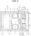
- an electric compressor (a so-called inverter-integrated electric compressor) 16 according to an embodiment integrally provided with a power conversion device 1 of the present invention will be described with reference to FIG. 2 .
- the electric compressor 16 of the embodiment constitutes a part of a refrigerant circuit of a vehicle air conditioning device mounted on a vehicle such as a hybrid car, an electric vehicle or the like and is powered and driven by a DC power supply (battery) 29 mounted on the vehicle.
- FIG. 2 the inside of a metal-made housing 2 of the electric compressor 16 is partitioned into a compression mechanism housing section 4 and an inverter housing section 6 by a partition wall 3 intersecting an axial direction of the housing 2.
- a scroll-type compression mechanism 7 and a motor 8 which drives this compression mechanism 7 are accommodated in the compression mechanism housing section 4.
- the motor 8 is an IPMSM (Interior Permanent Magnet Synchronous Motor) composed of a stator 9 fixed to the housing 2 and a permanent magnet built-in rotor 11 rotating inside the stator 9.
- IPMSM Interior Permanent Magnet Synchronous Motor
- a bearing portion 12 is formed at the central portion of the partition wall 3 on the compression mechanism housing section 4 side.
- One end of a drive shaft 13 of the rotor 11 is supported by the bearing portion 12, and the other end of the drive shaft 13 is linked to the compression mechanism 7.
- a suction port 14 is formed in the vicinity of the partition wall 3 at a position corresponding to the compression mechanism housing section 4 of the housing 2.
- the refrigerant compressed by the compression mechanism 7 and brought to a high temperature and high pressure is configured to be discharged from an unillustrated discharge port to the refrigerant circuit outside the housing 2. Further, since the low temperature refrigerant flowing from the suction port 14 passes near the partition wall 3 and passes around the motor 8, and is sucked by the compression mechanism 7, the partition wall 3 is also cooled.
- the power conversion device 1 is constituted of a substrate 17, six switching elements 18A to 18F wired on one surface side of the substrate 17, a control section 21 wired on the other surface side of the substrate 17, and an HV connector, an LV connector, etc. which are not shown in the drawing.
- each of the switching elements 18A to 18F is constituted of an insulated gate bipolar transistor (IGBT) or the like in which a MOS structure is incorporated in a gate portion.
- IGBT insulated gate bipolar transistor
- the switching element 18A on the upper arm side of a U-phase inverter 19U of a three-phase inverter circuit (three-phase inverter circuit) 28 to be described later and the switching element 18D on the lower arm side thereof, the switching element 18B on the upper arm side of a V-phase inverter 19V and the switching element 18E on the lower arm side thereof, and the switching element 18C on the upper arm side of a W-phase inverter 19W thereof and the switching element 18F on the lower arm side thereof are in the form of being arranged two by two respectively.
- the thus-arranged respective pairs of switching elements 18A and 18D, switching elements 18B and 18E, and switching elements 18C and 18F are radially disposed around the center of the substrate 17.
- the respective switching elements 18A to 18F are in close contact with the partition wall 3 directly or through a predetermined insulating heat conductive material and have a heat exchange relation with the partition wall 3 of the housing 2. Then, since the partition wall 3 is cooled by the refrigerant sucked into the compression mechanism housing section 4 as described above, the respective switching elements 18A to 18F are placed in heat exchange relation with the sucked refrigerant via the partition wall 3 and cooled by the refrigerant sucked into the compression mechanism housing section 4 through the thickness of the partition wall 3. The respective switching elements 18A to 18F themselves dissipate heat to the refrigerant through the partition wall 3.
- the power conversion device 1 includes the above-described three-phase inverter circuit (three-phase inverter circuit) 28 and control section 21.
- the inverter circuit 28 is a circuit which converts a DC voltage of the DC power supply (battery) 29 into a three-phase AC voltage and applies it to an armature coil of the stator 9 of the motor 8.
- This inverter circuit 28 has the U-phase inverter 19U, the V-phase inverter 19V, and the W-phase inverter 19W described above.
- the phase inverters 19U to 19W respectively have the switching elements 18A to 18C on the upper arm side described above, and the switching elements 18D to 18F on the lower arm side individually. Further, flywheel diodes 31 are connected in antiparallel to the switching elements 18A to 18F respectively.
- the upper end sides of the switching elements 18A to 18C on the upper arm side of the inverter circuit 28 are connected to the positive electrode sides of the DC power supply 29 and a smoothing capacitor 32.
- the smoothing capacitor 32 is also provided on the substrate 17 to constitute the power conversion device 1.
- the lower end sides of the switching elements 18D to 18F on the lower arm side of the inverter circuit 28 are connected to the negative electrode sides of the DC power supply 29 and the smoothing capacitor 32.
- the U-phase inverter 19U is connected to the U-phase armature coil of the motor 8 between the switching element 18A on the upper arm side and the switching element 18D on the lower arm side in the U-phase inverter 19.
- the V-phase inverter 19V is connected to the V-phase armature coil of the motor 8 between the switching element 18B on the upper arm side and the switching element 18E on the lower arm side in the V-phase inverter 19V.
- the W-phase inverter 19W is connected to the W-phase armature coil of the motor 8 between the switching element 18C on the upper arm side and the switching element 18F on the lower arm side in the W-phase inverter 19W.
- a current detector 30 for detecting a DC current flowing through the inverter circuit 28 is connected to a bus line between the DC power supply 29 and the inverter circuit 28.
- the current detector 30 is connected to the bus line on the minus side in the embodiment, but may be connected to the plus side.
- the current detector 30 can be constituted of a shunt resistor or a Hall element, but is assumed to consist of the shunt resistor in the embodiment.
- control section 21 is configured of a microcomputer having a processor.
- the control section 21 receives a rotation speed command value from a vehicle ECU, receives each phase current of a U-phase current iu, a V-phase current iv, and a W-phase current iw from the motor 8, and controls the ON/OFF states of the switching elements 18A to 18F of the inverter circuit 28, based on these.
- control section 21 controls a gate voltage applied to a gate terminal of each of the switching elements 18A to 18F.
- the control section 21 has a phase current converting unit 38, a phase voltage command calculating unit 33, a line modulation calculating unit 34, a PWM signal generating unit 36, a duty correcting unit 39, and a gate driver 37. Then, the phase voltage command calculating unit 33 and the line modulation calculating unit 34 constitute a command value calculating unit 35.
- the phase current converting unit 38 detects each phase current of the U-phase current iu, the V-phase current iv, and the W-phase current iw of the motor 8, based on the DC current detected by the current detector 30, and switching timings of the switching elements 18A to 18F.
- the switching element 18A on the upper arm side of the U-phase inverter 19U is turned ON
- the switching element 18E on the lower arm side of the V-phase inverter 19V and the switching element 18F on the lower arm side of the W-phase inverter 19W are turned ON
- the U-phase current iu flows from the switching element 18A to the U-phase armature coil of the motor 8
- the V-phase current iv flows from the flywheel diode 31 connected in parallel to the switching element 18E to the V-phase armature coil of the motor 8
- the W-phase current iw flows out from the W-phase armature coil of the motor 8 to the switching element 18F.
- the U-phase current iu flows through the current detector 30 to enable its detection.
- the switching element 18A on the upper arm side of the U-phase inverter 19U and the switching element 18B on the upper arm side of the V-phase inverter 19V are turned ON, and the switching element 18F on the lower arm side of the W-phase inverter 19W is turned ON, the U-phase current iu and the V-phase current iv flow from the switching elements 18A and 18B to the U-phase and V-phase armature coils of the motor 8, respectively, and the W-phase current iw flow out from the W-phase armature coil of the motor 8 to the switching element 18F.
- the W-phase current iw flows through the current detector 30 to enable its detection.
- the remaining V-phase current iv is obtained by applying the Kirchhoff's current law at the neutral point of the armature coil.
- the minimum time Y required for detecting the phase current by the current detector 30 exists in the phase current converting unit 38, and the ON period or OFF period of each of the switching elements 18A to 18C on the upper arm side is shorter than the minimum time Y within the carrier cycle, it becomes impossible to detect the phase current.
- the phase currents iu, iv, and iw detected by the phase current converting unit 38 are input to the phase voltage command calculating unit 33.
- the phase voltage command calculating unit 33 calculates sinusoidal modulation voltage command values U' (U-phase voltage command value), V' (V-phase voltage command value), and W' (W-phase voltage command value) each of which is applied to the armature coil of each phase of the motor 8, based on the electrical angle, current command value and phase currents iu, iv, and iw of the motor 8.
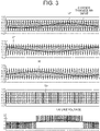
- the sinusoidal modulation voltage command values U', V', and W' are values after normalization (after correction to -1 to 1) of each voltage command value with the DC voltage Vdc where sinusoidal modulation control of the motor 8 is performed, and are shown in FIG. 3 .
- carrier triangular waves to be compared by the PWM signal generating unit 36 to be described later simultaneously.
- the frequency (carrier frequency) of the carrier triangular wave in the embodiment is set to 20kHz out of an audible range. This is because when the carrier frequency becomes a frequency in the audible range lower than 20 kHz, the sound generated from the electric compressor 16 is recognized as noise.
- Vu shown in FIG. 3 is a PWM signal (U phase) to be described later where the sinusoidal modulation control of the motor 8 is performed.
- the UV line voltage in FIG. 3 is a potential difference between the U phase and the V phase to be described later in the case where the sinusoidal modulation control is performed similarly.
- the line modulation calculating unit 34 calculates discontinuous modulation voltage command values U (U-phase voltage command value), V (V-phase voltage command value), and W (W-phase voltage command value) on the basis of the sinusoidal modulation voltage command values U', V', and W' arithmetically operated and calculated by the phase voltage command calculating unit 33. The operation of this line modulation calculating unit 34 will be described in detail later.
- the PWM signal generating unit 36 generates, based on the discontinuous modulation voltage command values U, V, and W arithmetically operated and calculated by the line modulation calculating unit 34, PWM signals Vu, Vv, and Vw which become drive command signals for the U-phase inverter 19U, the V-phase inverter 19V, and the W-phase inverter 19W of the inverter circuit 28, by comparing their magnitudes with the carrier triangular waves.
- the gate driver 37 generates, based on the PWM signals Vu, Vv, and Vw output from the PWM signal generating unit 36, gate voltages Vuu and Vul of the switching elements 18A and 18D of the U-phase inverter 19U, gate voltages Vvu and Vvl of the switching elements 18B and 18E of the V-phase inverter 19V, and gate voltages Vwu and Vwl of the switching elements 18C and 18F of the W-phase inverter 19W.
- the respective switching elements 18A to 18F of the inverter circuit 28 are ON/OFF driven based on the gate voltages Vuu, Vul, Vvu, Vvl, Vwu, and Vwl output from the gate driver 37. That is, when the gate voltage is brought into an ON state (predetermined voltage value), the transistor is ON-operated. When the gate voltage is brought into an OFF state (zero), the transistor is OFF-operated.
- the gate driver 37 is a circuit for applying a gate voltage to the IGBT, based on the PWM signal when each of the switching elements 18A to 18F is the above-described IGBT, and is comprised of a photocoupler, a logic IC, a transistor, or the like.
- the discontinuous modulation voltage command values U, V, and W calculated by the line modulation calculating unit 34 are values after normalization of each voltage command value for performing discontinuous modulation control of the motor 8 with the DC voltage Vdc (after correction to -1 to 1).
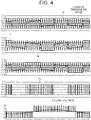
- An example is shown in FIG. 4 .
- the carrier triangular waves to be compared by the PWM signal generating unit 36 are also shown in FIG. 4 simultaneously.
- Vu shown in FIG. 4 is a PWM signal (U phase) for performing the discontinuous modulation control of the motor 8.
- a UV line voltage in FIG. 4 is a potential difference between the U-phase and the V phase in the discontinuous modulation control.
- the line modulation calculating unit 34 compares the U-phase voltage command value U', V-phase voltage command value V', and W-phase voltage command value W' each being the sinusoidal modulation voltage command value of each phase calculated by the phase voltage command calculating unit 33 to calculate and output the U-phase voltage command value U, V-phase voltage command value V, and W-phase voltage command value W being the discontinuous modulation voltage command values for fixing the ON/OFF states of the switching elements 18A to 18F of each phase maximized in absolute value to the ON or OFF states, thereby performing discontinuous modulation control to reduce the number of switching times of the switching elements 18A to 18F as compared with the case where the sinusoidal modulation control is performed.
- the maximum value K1 is greater than or equal to the absolute value of the minimum value K2, that is, when K1 ⁇ abs (K2), the maximum value K1 is taken to be K3.
- the absolute value of the minimum value K2 is greater than the maximum value K1, that is, when K1 ⁇ abs (K2), the minimum value K2 is taken to be K3.
- U U ′ ⁇ K + sign K
- V V ′ ⁇ K + sign K
- W W ′ ⁇ K + sign K
- the U-phase voltage command value U' when the U-phase voltage command value U' is K, the U-phase voltage command value U becomes "1" when the comparison value U' comp is the maximum value K1, and the U-phase voltage command value U becomes "-1" when the comparison value U' comp is the minimum value K2.
- the ON/OFF states of the switching elements 18A and 18D of the U-phase inverter 19U are fixed, and the number of times of switching is reduced correspondingly.
- the V-phase voltage command value V' is K
- the V-phase voltage command value V becomes "1" when the comparison value V' comp is the maximum value K1
- the V-phase voltage command value V becomes "-1" when the comparison value V' comp is the minimum value K2.
- the W-phase voltage command value W' is K
- the W-phase voltage command value W becomes "1" when the comparison value W' comp is the maximum value K1
- the W-phase voltage command value W becomes "-1" when the comparison value W' comp is the minimum value K2.
- FIG. 4 shows the U-phase voltage command value U, V-phase voltage command value V, and W-phase voltage command value W output from the line modulation calculating unit 34, the U-phase PWM signal Vu output from the PWM signal generating unit 36, and the UV line voltage.
- the ON/OFF states of the switching elements 18A and 18D of the U-phase inverter 19U are fixed.
- the ON/OFF states of the switching elements 18B and 18E of the V-phase inverter 19V are fixed, and the ON/OFF states of the switching elements 18C and 18F of the W-phase inverter 19W are fixed.
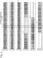
- FIG. 5 shows the discontinuous modulation voltage command values U, V, and W and the carrier triangular waves output by the line modulation calculating unit 34, and the PWM signals Vu, Vv, and Vw output by the PWM signal generating unit 36.
- FIG. 6 shows an enlarged view of the vicinity of a frame X in FIG. 5 .
- each of FIGS. 5 to 8 indicates the discontinuous modulation control in which the switching element on the upper arm side of any one phase is fixed to the OFF state, and the switching element on the lower arm side thereof is fixed to the ON state.
- the PWM signal Vu is a drive command signal for the U-phase inverter 19U of the inverter circuit 28, and the width of the pulse of "1" shown in FIGS. 5 and 6 is the duty within one carrier cycle, and becomes the ON period of the switching element 18A on the upper arm side. That is, during this duty (the width of the pulse of "1"), the switching element 18A on the upper arm side is turned ON, and the switching element 18D on the lower arm side is turned OFF.
- the PWM signal Vv is a drive command signal of the V-phase inverter 19V.
- the width of the pulse of "1" shown in FIGS. 5 and 6 is the duty within one carrier cycle, and becomes the ON period of the switching element 18B on the upper arm side. That is, during this duty (the width of the pulse of "1"), the switching element 18B on the upper arm side is turned ON, and the switching element 18E on the lower arm side is turned OFF.
- the PWM signal Vw is a drive command signal of the W-phase inverter 19W.
- the width of the pulse of "1" shown in FIGS. 5 and 6 is the duty within one carrier cycle, and becomes the ON period of the switching element 18C on the upper arm side. That is, during this duty (the width of the pulse of "1"), the switching element 18C on the upper arm side is turned ON, and the switching element 18F on the lower arm side is turned OFF.
- the switching element 18A on the upper arm side of the U phase is fixed to the OFF state. Then, when the phase current is detected during the ON periods of the switching elements 18B and 18C on the upper arm side of the V phase and the W phase, it becomes impossible to detect the phase currents of the V and W phases where the ON periods of the switching elements 18B and 18C on the upper arm side within one carrier cycle are shorter than this minimum time Y as shown in FIG. 6 . That is, although the U-phase current iu can be detected, the V-phase current iv and the W-phase current iw cannot be detected. It is therefore not possible to detect the phase currents iu, iv, and iw corresponding to the three phases.
- the duty correcting unit 39 of the control section 21 corrects the discontinuous modulation voltage command values U, V, and W output from the line modulation calculating unit 34 (the command value calculating unit 35) and corrects the PWM signals Vu, Vv, and Vw output from the PWM signal generating unit 36.
- a part of the ON period of the switching element 18B in the other V-phase carrier cycle Z2 is moved and added to the ON period of the switching element 18B on the upper arm side of the V phase in a V-phase specific carrier cycle Z1 shown in each of FIGS. 6 and 8 to correct the ON period (indicated by P1 in FIG. 8 ) of the switching element 18B in the V-phase specific carrier cycle Z1 to be greater than or equal to the above-mentioned minimum time Y.
- the ON period (indicated by P2 in FIG. 8 ) of the switching element 18B in the V-phase carrier cycle Z2 is set to the minimum value that can be output.
- the duty correcting unit 39 causes the sum of the duties of the switching elements 18B in the post-correction two carrier cycles (Z1 to Z2) shown in FIG. 8 to match with the sum of the duties of the switching element 18B in the two carrier cycles (Z1 to Z2) before the correction in FIG. 6 . Further, the duty correcting unit 39 provides the ON period of the switching element 18B in the first half of the specific carrier cycle Z1 of the V phase, and provides the ON period of the switching element 18B in the latter half of the other carrier cycle Z2 of the V phase.
- the duty correcting unit 39 moves and adds a part of the ON period of the switching element 18C in the other W-phase carrier cycle (next carrier cycle of Z2) to the ON period of the switching element 18C on the upper arm side of the W phase in a W-phase specific carrier cycle Z2 to correct the ON period (indicated by P3 in FIG. 8 ) of the switching element 18C in the specific carrier cycle Z2 of the W phase to be greater than or equal to the above-mentioned minimum time Y.
- the ON period of the switching element 18C in the other carrier cycle of the W phase is set to the minimum value that can be output in the same manner.
- the duty correcting unit 39 causes the sum of the duties of the switching element 18C in the post-correction two carrier cycles (Z2 and the next cycle) shown in FIG. 8 to match with the sum of the duties of the switching element 18C in the two carrier cycles (Z2 and the next cycle) before the correction in FIG. 6 . Further, the duty correcting unit 39 provides the ON period of the switching element 18C in the first half of the specific carrier cycle Z2 of the W phase, and provides the ON period of the switching element 18C in the latter half of the other carrier cycle (the cycle next to Z2) of the W phase.
- the above correction is similarly executed even with respect to other timings (a set of a specific carrier cycle and other carrier cycle).
- the other carrier cycle is not limited to one, and a part of each of those ON periods may be moved from two or more (plural) carrier cycles following the specific carrier cycle to the ON period of the specific carrier cycle.
- the phase current converting unit 38 can detect the V-phase current iv in the carrier cycle Z1 and the W-phase current iw in the carrier cycle Z2 by the current detector 30, and finally can detect the phase currents iu, iv, and iw corresponding to the three phases.
- the V-phase current iv and the W-phase current iw can be detected without any trouble.
- the switching element 18C is also switched in the carrier cycle Z1 and the switching element 18B is also switched in the carrier cycle Z2, the carrier cycle does not change.
- the duty correcting unit 39 of the control section 21 moves and adds the part of the ON period of the switching element (18B in the V phase) in the other carrier cycle (Z2 in the V phase) to the ON period of the switching element (18B in the V phase) of the inverter circuit 28 in the specific carrier cycle (Z1 in the V phase) to thereby correct the ON period of the switching element (18B in the V phase) in the specific carrier cycle (Z1 in the V phase) to be greater than or equal to the minimum time Y required for detecting the current by the current detector 30.
- the power conversion device 1 of the discontinuous modulation method as in the embodiment even when as in the embodiment, the voltage utilization rate kH of the motor 8 becomes low and thereby as in the embodiment, the OFF state of the switching element 18A on the upper arm side of the U phase in the inverter circuit 28 is fixed, and the ON periods of the switching elements 18B and 18C on the upper arm side of the other two phases become shorter than the minimum time Y within one carrier cycle, it is possible to secure the ON period greater than or equal to the minimum time Y for detecting the current by the current detector 30 in the specific carrier cycle (Z1 in the V phase) and detect the phase current (iv in the V-phase carrier cycle Z1).
- the duty correcting unit 39 adds the part of the ON period of the switching element (18B in the V phase) in the other carrier cycle (Z2 in the V phase) to the ON period of the switching element (18B) in the specific carrier cycle (Z1 in the V phase), the generation of noise due to a decrease in the carrier frequency can also be prevented.
- the duty correcting unit 39 makes the sums of the duties in the specific carrier cycle (Z1 in the V phase) and in the other carrier cycle (Z2 in the V phase) match before and after the correction. It is therefore possible to achieve high-quality motor control without causing deterioration of the controllability of the motor 8 as well.
- the duty correcting unit 39 corrects the corrected ON period of the switching element (18B in the V phase) in the other carrier cycle (Z2 in the V phase) to be the minimum value that can be output. Therefore, even if the motor 8 is rotated at a low speed, it is possible to secure the ON period of the minimum time Y or more for current detection by the current detector 30 in the specific carrier cycle (Z1 in the V phase) without any problem.
- the duty correcting unit 39 provides the corrected ON period of the switching element (18B in the V phase) in the first half of the specific carrier cycle (Z1 in the V phase), and provides the corrected ON period of the switching element (18B in the V phase) in the latter half of the other carrier cycle (Z2 in the V phase). Therefore, the phase of the ON period does not overlap with other phases, and the phase currents iv and iw can be easily detected in the specific carrier cycles (Z1 in the V phase and Z2 in the W phase).
- the part of the ON period of the switching element in the other carrier cycle is moved and added to the ON period of the switching element of the inverter circuit 28 in the specific carrier cycle.
- the part of the OFF period of the switching element in the other carrier cycle is moved and added to the OFF period of the switching element in the specific carrier cycle.
- the OFF period of the switching element in the specific carrier cycle may be corrected to be equal to or longer than the minimum time Y required for detecting the current by the current detector 30.
- the duty correcting unit corrects the sinusoidal modulation voltage command values U', V', and W' output by the phase voltage command calculating unit 33 in the same manner as described above.
- the present invention is applied to the power conversion device 1 which drives and controls the motor 8 of the electric compressor 16, but the present invention is not limited thereto.
- the present invention is effective for the drive control of the motors of various devices.
Landscapes
- Engineering & Computer Science (AREA)
- Power Engineering (AREA)
- Inverter Devices (AREA)
Abstract
Description
- The present invention relates to a power conversion device which supplies power to a motor to drive the same.
- Conventionally, a power conversion device for driving a motor performs PWM (Pulse Width Modulation) control of switching elements of UVW respective phases of a three-phase inverter circuit, but one current detector (shunt resistor or Hall element) detecting a DC current between a DC power supply and the inverter circuit is provided to detect a phase current that becomes information to estimate the position of a rotor (rotating member) with a permanent magnet built therein, and the phase currents of two phases of UVW are detected from the DC current detected by the current detector and the switching timing of the switching element, finally resulting in obtaining the phase current of each phase (refer to, for example, Patent Document 1).
- Further, in recent years, a power conversion device (inverter device) in which a method called discontinuous modulation is applied to a PWM control unit has also been proposed for the purpose of reducing loss and heat generation of switching elements. This power conversion device of discontinuous modulation method fixes an ON/OFF state of any one of UVW respective phases and controls only other two phases while modulating the ON/OFF state, thereby performing PWM control while reducing the number of switching times of the switching element as compared with a sinusoidal modulation method and decreasing a switching loss and a heat generation amount (refer to, for example, Patent Document 2).
-
- Patent Document 1:
Japanese Patent No. 4788416 - Patent Document 2:
Japanese Patent Application Laid-Open No. Hei-8(1996)-340691 - Here, in
Patent Document 1 described above, when the switching element on the upper arm side of the W phase is turned ON for substantially the entire period within a carrier cycle, and the switching element on the upper arm side of the V phase is turned OFF, the period during which the switching element on the upper arm side of the U phase is turned ON becomes shorter and is made shorter than the minimum time required for detecting the current by the current detector. When the phase currents for two phases cannot be detected, there has been performed a correction in which the ON periods of the switching element on the upper arm side of the U phase in the two carrier cycles are collected in one carrier cycle, and no energization is done for the remaining carrier cycle (for example, FIG. 10 (b) of Patent Document 1). - However, when the above correction is performed, the carrier frequency is halved because the U-phase switching element is switched at every other carrier cycle. On the other hand, a problem arises in that since the carrier frequency is usually set to a value out of an audible region, noise is generated at the half carrier frequency.
- The present invention has been made to solve such conventional technical problems. The present invention provides a power conversion device capable of detecting a phase current without generating noise and without any trouble even in situations in which a motor is rotated at a low speed and thereby it becomes difficult to detect a DC current flowing through an inverter circuit.
- A power conversion device of the present invention includes an inverter circuit which drives a motor, a current detector which detects a DC current flowing through the inverter circuit, a command value calculating unit which calculates a voltage command value to be applied to the motor, based on the current value detected by the current detector, a PWM signal generating unit which generates a PWM signal to PWM-control the inverter circuit, based on the voltage command value calculated by the command value calculating unit, and a duty correcting unit which corrects a duty of the PWM signal generated by the PWM signal generating unit. The power conversion device is characterized in that the duty correcting unit moves and adds a part of an ON period of one of switching elements of the inverter circuit in the other carrier cycle to an ON period of the switching element in a specific carrier cycle or moves and adds a part of an OFF period of the switching element in the other carrier cycle to an OFF period of the switching element in the specific carrier cycle to correct the ON period or OFF period of the switching element in the specific carrier cycle to be greater than or equal to a minimum time required for detecting the current by the current detector.
- The power conversion device of the invention of
claim 2 is characterized in that in the above invention, the duty correcting unit causes the sums of duties in the specific carrier cycle and the other carrier cycle to match with each other before and after the correction. - The power conversion device of the invention of
claim 3 is characterized in that in the above respective inventions, the duty correcting unit corrects the corrected ON period or OFF period of the switching element in the other carrier cycle to be an outputtable minimum value. - The power conversion device of the invention of
claim 4 is characterized in that in the above respective inventions, the duty correcting unit provides the corrected ON period or OFF period of the switching element in the first half of the specific carrier cycle. - The power conversion device of the invention of claim 5 is characterized in that in the above invention, the duty correcting unit provides the corrected ON period or OFF period of the switching element in the latter half of the other carrier cycle.
- The power conversion device of the invention of
claim 6 is characterized in that in the above respective inventions, when a voltage utilization rate of the motor which is a square average of normalized voltage command values drops to a predetermined voltage utilization rate or less, the duty correcting unit corrects the ON period or OFF period of the switching element in the specific carrier cycle and the other carrier cycle. - The power conversion device of the invention of
claim 7 is characterized in that in the above respective inventions, the command value calculating unit includes a phase voltage command calculating unit which calculates sinusoidal modulation voltage command values to be applied to the motor, and a line modulation calculating unit which, based on the sinusoidal modulation voltage command values, calculates discontinuous modulation voltage command values for fixing an ON/OFF state of the switching element of a predetermined one phase in the inverter circuit and modulating ON/OFF states of the switching elements of other two phases, and in that the PWM signal generating unit generates PWM signals to PWM-control the inverter circuit, based on the discontinuous modulation voltage command values calculated by the line modulation calculating unit. - The power conversion device of the invention of
claim 8 is characterized in that in the above invention, when an OFF state of the switching element on the upper arm side of the one phase in the inverter circuit is fixed, and an ON period of each of the switching elements on the upper arm side of other two phases is shorter than the minimum time within one carrier cycle, or when an ON state of the switching element on the upper arm side of the one phase is fixed, and an OFF period of each of the switching elements on the upper arm side of other two phases is shorter than the minimum time within one carrier cycle, the duty correcting unit corrects the ON period or OFF period of the switching element in the specific carrier cycle and the other carrier cycle. - According to the present invention, in a power conversion device including an inverter circuit which drives a motor, a current detector which detects a DC current flowing through the inverter circuit, a command value calculating unit which calculates a voltage command value to be applied to the motor, based on the current value detected by the current detector, a PWM signal generating unit which generates a PWM signal to PWM-control the inverter circuit, based on the voltage command value calculated by the command value calculating unit, and a duty correcting unit which corrects a duty of the PWM signal generated by the PWM signal generating unit, the duty correcting unit moves and adds a part of an ON period of one of switching elements of the inverter circuit in the other carrier cycle to an ON period of the switching element in a specific carrier cycle or moves and adds a part of an OFF period of the switching element in the other carrier cycle to an OFF period of the switching element in the specific carrier cycle to correct the ON period or OFF period of the switching element in the specific carrier cycle to be greater than or equal to a minimum time required for detecting the current by the current detector. Therefore, for example, in the power conversion device of the discontinuous modulation method as in the invention of
claim 7, even when as in the invention ofclaim 6, a voltage utilization rate of the motor becomes low and thereby as in the invention ofclaim 8, for example, the OFF state of the switching element on the upper arm side of one phase in the inverter circuit is fixed, and the ON periods of the switching elements on the upper arm side of the other two phases become shorter than the minimum time within one carrier cycle, or even when the ON state of the switching element on the upper arm side of one phase is fixed, and the OFF periods of the switching elements on the upper arm side of other two phases become shorter than the minimum time within one carrier cycle, it is possible to secure the ON period or OFF period greater than or equal to the minimum time for detecting the current by the current detector in the specific carrier cycle and detect the phase current. - In particular, since the duty correcting unit adds the part of the ON period or OFF period of the switching element in the other carrier cycle to the ON period or OFF period of the switching element in the specific carrier cycle, the generation of noise due to a decrease in the carrier frequency can also be prevented.
- Also, according to the invention of
claim 2, since the duty correcting unit matches the sums of the duties in the specific carrier cycle and the other carrier cycle with each other before and after the correction in addition to the above invention, it is possible to achieve high-quality motor control without causing deterioration of the controllability of the motor as well. - In this case, as in the invention of
claim 3, if the duty correcting unit corrects the corrected ON period or OFF period of the switching element in the other carrier cycle to be the minimum value that can be output, it is possible to secure the ON period or OFF period of the minimum time or more for current detection by the current detector in the specific carrier cycle without any problem even if the motor is rotated at a low speed. - Further, if the duty correcting unit provides the corrected ON period or OFF period of the switching element in the first half of the specific carrier cycle as in the invention of
claim 4, and provides the corrected ON period or OFF period of the switching element in the latter half of the other carrier cycle as in the invention of claim 5, the phase of the ON period or OFF period does not overlap with other phases, and the phase current can be easily detected in the specific carrier cycle. -
-
FIG. 1 is an electric circuit diagram of a power conversion device according to one embodiment of the present invention. -
FIG. 2 is a longitudinal cross-sectional side view of an electric compressor of one embodiment provided with the power conversion device ofFIG. 1 . -
FIG. 3 is a diagram showing sinusoidal modulation voltage command values and carrier triangular waves output by a phase voltage command calculating unit constituting a command value calculating unit of a control section ofFIG. 1 , and a PWM waveform and a UV line voltage when performing sinusoidal modulation control. -
FIG. 4 is a diagram showing discontinuous modulation voltage command values and carrier triangular waves output by a line modulation calculating unit constituting a command value calculating unit of the control section ofFIG. 1 , and a PWM waveform and a UV line voltage output by a PWM signal generating unit. -
FIG. 5 is a diagram showing discontinuous modulation voltage command values and carrier triangular waves output by the line modulation calculating unit constituting the command value calculating unit of the control section ofFIG. 1 , and a PWM waveform and a line voltage output by the PWM signal generating unit. -
FIG. 6 is an enlarged diagram of the vicinity of a frame X inFIG. 5 . -
FIG. 7 is a diagram showing discontinuous modulation voltage command values and carrier triangular waves output by the line modulation calculating unit constituting the command value calculating unit of the control section ofFIG, 1 , and a PWM waveform and a line voltage output and corrected by a duty correcting unit. -
FIG. 8 is an enlarged diagram of the vicinity of a frame X ofFIG. 7 . - Hereinafter, embodiments of the present invention will be described in detail based on the drawings. First, an electric compressor (a so-called inverter-integrated electric compressor) 16 according to an embodiment integrally provided with a
power conversion device 1 of the present invention will be described with reference toFIG. 2 . Incidentally, theelectric compressor 16 of the embodiment constitutes a part of a refrigerant circuit of a vehicle air conditioning device mounted on a vehicle such as a hybrid car, an electric vehicle or the like and is powered and driven by a DC power supply (battery) 29 mounted on the vehicle. - In
FIG. 2 , the inside of a metal-madehousing 2 of theelectric compressor 16 is partitioned into a compressionmechanism housing section 4 and aninverter housing section 6 by apartition wall 3 intersecting an axial direction of thehousing 2. For example, a scroll-type compression mechanism 7 and amotor 8 which drives thiscompression mechanism 7 are accommodated in the compressionmechanism housing section 4. In this case, themotor 8 is an IPMSM (Interior Permanent Magnet Synchronous Motor) composed of astator 9 fixed to thehousing 2 and a permanent magnet built-inrotor 11 rotating inside thestator 9. - A
bearing portion 12 is formed at the central portion of thepartition wall 3 on the compressionmechanism housing section 4 side. One end of adrive shaft 13 of therotor 11 is supported by thebearing portion 12, and the other end of thedrive shaft 13 is linked to thecompression mechanism 7. Asuction port 14 is formed in the vicinity of thepartition wall 3 at a position corresponding to the compressionmechanism housing section 4 of thehousing 2. When the rotor 11 (drive shaft 13) of themotor 8 is rotated to drive thecompression mechanism 7, a refrigerant which is a working fluid, flows from thesuction port 14 into the compressionmechanism housing section 4 of thehousing 2 and is sucked into and compressed by thecompression mechanism 7. - Then, the refrigerant compressed by the
compression mechanism 7 and brought to a high temperature and high pressure is configured to be discharged from an unillustrated discharge port to the refrigerant circuit outside thehousing 2. Further, since the low temperature refrigerant flowing from thesuction port 14 passes near thepartition wall 3 and passes around themotor 8, and is sucked by thecompression mechanism 7, thepartition wall 3 is also cooled. - And then, the
power conversion device 1 of the present invention which drives and controls themotor 8 is housed in theinverter housing section 6 partitioned from the compressionmechanism housing section 4 by thepartition wall 3. In this case, thepower conversion device 1 is configured to supply power to themotor 8 through a sealing terminal and a lead wire penetrating thepartition wall 3. - In the case of the embodiment, the
power conversion device 1 is constituted of asubstrate 17, sixswitching elements 18A to 18F wired on one surface side of thesubstrate 17, acontrol section 21 wired on the other surface side of thesubstrate 17, and an HV connector, an LV connector, etc. which are not shown in the drawing. In the embodiment, each of theswitching elements 18A to 18F is constituted of an insulated gate bipolar transistor (IGBT) or the like in which a MOS structure is incorporated in a gate portion. - In this case, in the embodiment, the
switching element 18A on the upper arm side of aU-phase inverter 19U of a three-phase inverter circuit (three-phase inverter circuit) 28 to be described later and theswitching element 18D on the lower arm side thereof, theswitching element 18B on the upper arm side of a V-phase inverter 19V and theswitching element 18E on the lower arm side thereof, and theswitching element 18C on the upper arm side of a W-phase inverter 19W thereof and theswitching element 18F on the lower arm side thereof are in the form of being arranged two by two respectively. The thus-arranged respective pairs ofswitching elements elements elements substrate 17. - Further,
terminal portions 22 of therespective switching elements 18A to 18F are connected to thesubstrate 17 in a state in which they are on the center side of thesubstrate 17. Then, in a state in which one surface side of therespective switching elements 18A to 18F being present is on thepartition wall 3 side, thepower conversion device 1 assembled in this manner is accommodated in theinverter housing section 6, attached to thepartition wall 3 and closed with acover 23. In this case, thesubstrate 17 is fixed to thepartition wall 3 viaboss portions 24 which stand up from thepartition wall 3. - Thus, in the state in which the
power conversion device 1 is attached to thepartition wall 3, therespective switching elements 18A to 18F are in close contact with thepartition wall 3 directly or through a predetermined insulating heat conductive material and have a heat exchange relation with thepartition wall 3 of thehousing 2. Then, since thepartition wall 3 is cooled by the refrigerant sucked into the compressionmechanism housing section 4 as described above, therespective switching elements 18A to 18F are placed in heat exchange relation with the sucked refrigerant via thepartition wall 3 and cooled by the refrigerant sucked into the compressionmechanism housing section 4 through the thickness of thepartition wall 3. Therespective switching elements 18A to 18F themselves dissipate heat to the refrigerant through thepartition wall 3. - Next, in
FIG. 1 , thepower conversion device 1 according to the embodiment of the present invention includes the above-described three-phase inverter circuit (three-phase inverter circuit) 28 andcontrol section 21. Theinverter circuit 28 is a circuit which converts a DC voltage of the DC power supply (battery) 29 into a three-phase AC voltage and applies it to an armature coil of thestator 9 of themotor 8. Thisinverter circuit 28 has theU-phase inverter 19U, the V-phase inverter 19V, and the W-phase inverter 19W described above. Thephase inverters 19U to 19W respectively have theswitching elements 18A to 18C on the upper arm side described above, and theswitching elements 18D to 18F on the lower arm side individually. Further,flywheel diodes 31 are connected in antiparallel to theswitching elements 18A to 18F respectively. - Then, the upper end sides of the
switching elements 18A to 18C on the upper arm side of theinverter circuit 28 are connected to the positive electrode sides of theDC power supply 29 and a smoothingcapacitor 32. Incidentally, the smoothingcapacitor 32 is also provided on thesubstrate 17 to constitute thepower conversion device 1. On the other hand, the lower end sides of theswitching elements 18D to 18F on the lower arm side of theinverter circuit 28 are connected to the negative electrode sides of theDC power supply 29 and the smoothingcapacitor 32. - And then, the
U-phase inverter 19U is connected to the U-phase armature coil of themotor 8 between the switchingelement 18A on the upper arm side and theswitching element 18D on the lower arm side in the U-phase inverter 19. The V-phase inverter 19V is connected to the V-phase armature coil of themotor 8 between the switchingelement 18B on the upper arm side and theswitching element 18E on the lower arm side in the V-phase inverter 19V. The W-phase inverter 19W is connected to the W-phase armature coil of themotor 8 between the switchingelement 18C on the upper arm side and theswitching element 18F on the lower arm side in the W-phase inverter 19W. - Further, a
current detector 30 for detecting a DC current flowing through theinverter circuit 28 is connected to a bus line between theDC power supply 29 and theinverter circuit 28. Thecurrent detector 30 is connected to the bus line on the minus side in the embodiment, but may be connected to the plus side. Also, thecurrent detector 30 can be constituted of a shunt resistor or a Hall element, but is assumed to consist of the shunt resistor in the embodiment. - Next, the
control section 21 is configured of a microcomputer having a processor. Thecontrol section 21 receives a rotation speed command value from a vehicle ECU, receives each phase current of a U-phase current iu, a V-phase current iv, and a W-phase current iw from themotor 8, and controls the ON/OFF states of theswitching elements 18A to 18F of theinverter circuit 28, based on these. Specifically, thecontrol section 21 controls a gate voltage applied to a gate terminal of each of theswitching elements 18A to 18F. - The
control section 21 has a phase current convertingunit 38, a phase voltagecommand calculating unit 33, a linemodulation calculating unit 34, a PWMsignal generating unit 36, aduty correcting unit 39, and agate driver 37. Then, the phase voltagecommand calculating unit 33 and the linemodulation calculating unit 34 constitute a commandvalue calculating unit 35. - The phase current converting
unit 38 detects each phase current of the U-phase current iu, the V-phase current iv, and the W-phase current iw of themotor 8, based on the DC current detected by thecurrent detector 30, and switching timings of theswitching elements 18A to 18F. - For example, in an energization pattern in which within a carrier cycle, the switching
element 18A on the upper arm side of theU-phase inverter 19U is turned ON, the switchingelement 18E on the lower arm side of the V-phase inverter 19V and theswitching element 18F on the lower arm side of the W-phase inverter 19W are turned ON, the U-phase current iu flows from the switchingelement 18A to the U-phase armature coil of themotor 8, the V-phase current iv flows from theflywheel diode 31 connected in parallel to theswitching element 18E to the V-phase armature coil of themotor 8, and the W-phase current iw flows out from the W-phase armature coil of themotor 8 to theswitching element 18F. In this case, the U-phase current iu flows through thecurrent detector 30 to enable its detection. - On the other hand, in an energization pattern in which within a carrier cycle, the switching
element 18A on the upper arm side of theU-phase inverter 19U and theswitching element 18B on the upper arm side of the V-phase inverter 19V are turned ON, and theswitching element 18F on the lower arm side of the W-phase inverter 19W is turned ON, the U-phase current iu and the V-phase current iv flow from theswitching elements motor 8, respectively, and the W-phase current iw flow out from the W-phase armature coil of themotor 8 to theswitching element 18F. In this case, the W-phase current iw flows through thecurrent detector 30 to enable its detection. - From the U-phase current iu and W-phase current iw obtained in this way, the remaining V-phase current iv is obtained by applying the Kirchhoff's current law at the neutral point of the armature coil. Incidentally, when the minimum time Y required for detecting the phase current by the
current detector 30 exists in the phase current convertingunit 38, and the ON period or OFF period of each of theswitching elements 18A to 18C on the upper arm side is shorter than the minimum time Y within the carrier cycle, it becomes impossible to detect the phase current. Then, the phase currents iu, iv, and iw detected by the phase current convertingunit 38 are input to the phase voltagecommand calculating unit 33. - The phase voltage
command calculating unit 33 calculates sinusoidal modulation voltage command values U' (U-phase voltage command value), V' (V-phase voltage command value), and W' (W-phase voltage command value) each of which is applied to the armature coil of each phase of themotor 8, based on the electrical angle, current command value and phase currents iu, iv, and iw of themotor 8. The sinusoidal modulation voltage command values U', V', and W' are values after normalization (after correction to -1 to 1) of each voltage command value with the DC voltage Vdc where sinusoidal modulation control of themotor 8 is performed, and are shown inFIG. 3 . - Incidentally, there are also shown in
FIG. 3 , carrier triangular waves to be compared by the PWMsignal generating unit 36 to be described later simultaneously. The frequency (carrier frequency) of the carrier triangular wave in the embodiment is set to 20kHz out of an audible range. This is because when the carrier frequency becomes a frequency in the audible range lower than 20 kHz, the sound generated from theelectric compressor 16 is recognized as noise. Also, in terms of the carrier frequency, Vu shown inFIG. 3 is a PWM signal (U phase) to be described later where the sinusoidal modulation control of themotor 8 is performed. The UV line voltage inFIG. 3 is a potential difference between the U phase and the V phase to be described later in the case where the sinusoidal modulation control is performed similarly. - The line
modulation calculating unit 34 calculates discontinuous modulation voltage command values U (U-phase voltage command value), V (V-phase voltage command value), and W (W-phase voltage command value) on the basis of the sinusoidal modulation voltage command values U', V', and W' arithmetically operated and calculated by the phase voltagecommand calculating unit 33. The operation of this linemodulation calculating unit 34 will be described in detail later. - The PWM
signal generating unit 36 generates, based on the discontinuous modulation voltage command values U, V, and W arithmetically operated and calculated by the linemodulation calculating unit 34, PWM signals Vu, Vv, and Vw which become drive command signals for theU-phase inverter 19U, the V-phase inverter 19V, and the W-phase inverter 19W of theinverter circuit 28, by comparing their magnitudes with the carrier triangular waves. - The
duty correcting unit 39 corrects the discontinuous modulation voltage command values U, V, and W output from the line modulation calculating unit 34 (command value calculating unit 35) to thereby correct the PWM signals Vu, Vv, and Vw output from the PWMsignal generating unit 36 and to be output to thegate driver 37. However, the operation of theduty correcting unit 39 will also be described in detail later. - The
gate driver 37 generates, based on the PWM signals Vu, Vv, and Vw output from the PWMsignal generating unit 36, gate voltages Vuu and Vul of theswitching elements U-phase inverter 19U, gate voltages Vvu and Vvl of the switchingelements phase inverter 19V, and gate voltages Vwu and Vwl of theswitching elements phase inverter 19W. These gate voltages Vuu, Vul, Vvu, Vvl, Vwu, and Vwl can be represented by a duty (ON period of each of theswitching elements 18A to 18C on the upper arm side) which is a time ratio of an ON state in a predetermined time. - Then, the
respective switching elements 18A to 18F of theinverter circuit 28 are ON/OFF driven based on the gate voltages Vuu, Vul, Vvu, Vvl, Vwu, and Vwl output from thegate driver 37. That is, when the gate voltage is brought into an ON state (predetermined voltage value), the transistor is ON-operated. When the gate voltage is brought into an OFF state (zero), the transistor is OFF-operated. Thegate driver 37 is a circuit for applying a gate voltage to the IGBT, based on the PWM signal when each of theswitching elements 18A to 18F is the above-described IGBT, and is comprised of a photocoupler, a logic IC, a transistor, or the like. - Next, the computation/calculation operation of the discontinuous modulation voltage command values U, V, and W in the line
modulation calculating unit 34 constituting the commandvalue calculating unit 35 of thecontrol section 21 will be described with reference toFIG. 4 . The discontinuous modulation voltage command values U, V, and W calculated by the linemodulation calculating unit 34 are values after normalization of each voltage command value for performing discontinuous modulation control of themotor 8 with the DC voltage Vdc (after correction to -1 to 1). An example is shown inFIG. 4 . Incidentally, the carrier triangular waves to be compared by the PWMsignal generating unit 36 are also shown inFIG. 4 simultaneously. Further, Vu shown inFIG. 4 is a PWM signal (U phase) for performing the discontinuous modulation control of themotor 8. A UV line voltage inFIG. 4 is a potential difference between the U-phase and the V phase in the discontinuous modulation control. - The line
modulation calculating unit 34 compares the U-phase voltage command value U', V-phase voltage command value V', and W-phase voltage command value W' each being the sinusoidal modulation voltage command value of each phase calculated by the phase voltagecommand calculating unit 33 to calculate and output the U-phase voltage command value U, V-phase voltage command value V, and W-phase voltage command value W being the discontinuous modulation voltage command values for fixing the ON/OFF states of theswitching elements 18A to 18F of each phase maximized in absolute value to the ON or OFF states, thereby performing discontinuous modulation control to reduce the number of switching times of theswitching elements 18A to 18F as compared with the case where the sinusoidal modulation control is performed. - Next, specific comparison calculation and fixed phase determination control therefor will be described in detail. First, when comparing the sinusoidal modulation voltage command values U', V', and W' as described above, the line
modulation calculating unit 34 of the embodiment puts the respective values as comparison values U' comp, V' comp, and W' comp as in the following equations (i) to (iii):


- Next, the respective comparison values U' comp, V' comp, and W' comp are compared by the equations (iv) and (v) to calculate the maximum value K1 and the minimum value K2 of them:


- When the maximum value K1 is greater than or equal to the absolute value of the minimum value K2, that is, when K1≥abs (K2), the maximum value K1 is taken to be K3. When the absolute value of the minimum value K2 is greater than the maximum value K1, that is, when K1<abs (K2), the minimum value K2 is taken to be K3.
- Then, when K3 is the comparison value U' comp, that is, when K3 = U' comp, the U-phase voltage command value U' is taken to be K. Further, when K3 is the comparison value V' comp, that is, when K3 = V' comp, the V-phase voltage command value V' is taken to be K. When K3 is the comparison value W' comp, that is, K3 = W' comp, the W-phase voltage command value W' is taken to be K.
- After K is determined in this manner, the U-phase voltage command value U, V-phase voltage command value V, and W-phase voltage command value W each being the discontinuous modulation voltage command value are calculated using the following equations (vi) to (viii):


- However, sign (K) is assumed to become "1" when K is a positive value, and is assumed to become "-1" when K is a negative value. Further, it can be seen from the respective equations (vi) to (viii) that the line voltage does not change in the sinusoidal modulation control and the discontinuous modulation control.
- Accordingly, when the U-phase voltage command value U' is K, the U-phase voltage command value U becomes "1" when the comparison value U' comp is the maximum value K1, and the U-phase voltage command value U becomes "-1" when the comparison value U' comp is the minimum value K2. Thus, during a period in which the U-phase voltage command value U' is K, the ON/OFF states of the
switching elements U-phase inverter 19U are fixed, and the number of times of switching is reduced correspondingly. - Also, in the case where the V-phase voltage command value V' is K, the V-phase voltage command value V becomes "1" when the comparison value V' comp is the maximum value K1, and the V-phase voltage command value V becomes "-1" when the comparison value V' comp is the minimum value K2. Thus, during a period in which the V-phase voltage command value V' is K, the ON/OFF states of the switching
elements phase inverter 19V are fixed, and the number of times of switching is reduced correspondingly. - Further, in the case where the W-phase voltage command value W' is K, the W-phase voltage command value W becomes "1" when the comparison value W' comp is the maximum value K1, and the W-phase voltage command value W becomes "-1" when the comparison value W' comp is the minimum value K2. Thus, during a period in which the W-phase voltage command value W' is K, the ON/OFF states of the
switching elements phase inverter 19W are fixed, and the number of times of switching is reduced correspondingly. -
FIG. 4 shows the U-phase voltage command value U, V-phase voltage command value V, and W-phase voltage command value W output from the linemodulation calculating unit 34, the U-phase PWM signal Vu output from the PWMsignal generating unit 36, and the UV line voltage. In this figure, during a period in which the U-phase voltage command value U becomes "1" or "-1", the ON/OFF states of theswitching elements U-phase inverter 19U are fixed. During a period in which the V-phase voltage command value V is "1" or "-1", the ON/OFF states of the switchingelements phase inverter 19V are fixed, and the ON/OFF states of theswitching elements phase inverter 19W are fixed. - Thus, when the total number of switchings per period of the
switching elements 18A to 18F of each phase in the sinusoidal modulation control is defined as 6/6 (U phase) + 6/6 (V phase) + 6/6 (W phase) = 18/6, the number of switching times of theswitching elements 18A to 18F of each phase is reduced to 2/3 in any case and becomes 4/6 (U phase) + 4/6 (V phase) + 4/6 (W phase) = 12/6 in the discontinuous modulation control as shown inFIG. 4 . Therefore, according to the discontinuous modulation control, a switching loss generated in each of theswitching elements 18A to 18F and heat generation due to it are suppressed as compared with the sinusoidal modulation control. - Next, the correcting operation of each PWM signal by the
duty correcting unit 39 within the carrier cycle will be described in detail with reference toFIGS. 5 to 8 .FIG. 5 shows the discontinuous modulation voltage command values U, V, and W and the carrier triangular waves output by the linemodulation calculating unit 34, and the PWM signals Vu, Vv, and Vw output by the PWMsignal generating unit 36.FIG. 6 shows an enlarged view of the vicinity of a frame X inFIG. 5 . - The example shown in each of
FIGS. 5 to 8 indicates the discontinuous modulation control in which the switching element on the upper arm side of any one phase is fixed to the OFF state, and the switching element on the lower arm side thereof is fixed to the ON state. - As described above, the PWM signal Vu is a drive command signal for the
U-phase inverter 19U of theinverter circuit 28, and the width of the pulse of "1" shown inFIGS. 5 and6 is the duty within one carrier cycle, and becomes the ON period of theswitching element 18A on the upper arm side. That is, during this duty (the width of the pulse of "1"), the switchingelement 18A on the upper arm side is turned ON, and theswitching element 18D on the lower arm side is turned OFF. - Further, the PWM signal Vv is a drive command signal of the V-
phase inverter 19V. Similarly, the width of the pulse of "1" shown inFIGS. 5 and6 is the duty within one carrier cycle, and becomes the ON period of theswitching element 18B on the upper arm side. That is, during this duty (the width of the pulse of "1"), the switchingelement 18B on the upper arm side is turned ON, and theswitching element 18E on the lower arm side is turned OFF. - In addition, the PWM signal Vw is a drive command signal of the W-
phase inverter 19W. Similarly, the width of the pulse of "1" shown inFIGS. 5 and6 is the duty within one carrier cycle, and becomes the ON period of theswitching element 18C on the upper arm side. That is, during this duty (the width of the pulse of "1"), the switchingelement 18C on the upper arm side is turned ON, and theswitching element 18F on the lower arm side is turned OFF. - In such a
power conversion device 1, when a voltage utilization rate kH of themotor 8 decreases, for example, in a region near the frame X inFIG. 5 , as shown inFIG. 6 , the switchingelement 18A on the upper arm side of the U phase is fixed to the OFF state, theswitching element 18D on the lower arm side is fixed to the ON state ("-1"), and the ON period ("1") of theswitching element 18B on the upper arm side of the V phase and the ON period ("1") of theswitching element 18C on the upper arm side of the W phase become extremely short. Here, the voltage utilization rate kH can be expressed by the following equation (ix) when expressed by the U-phase voltage command value U', the V-phase voltage command value V', and the W-phase voltage command value W', which are the three-phase voltage command values of each phase:
- On the other hand, as described above, since the minimum time Y required for detecting the phase current by the
current detector 30 exists in the phase current convertingunit 38, the switchingelement 18A on the upper arm side of the U phase is fixed to the OFF state. Then, when the phase current is detected during the ON periods of the switchingelements elements FIG. 6 . That is, although the U-phase current iu can be detected, the V-phase current iv and the W-phase current iw cannot be detected. It is therefore not possible to detect the phase currents iu, iv, and iw corresponding to the three phases. - Therefore, in the embodiment, when the voltage utilization rate kH of the
motor 8 drops to a predetermined voltage utilization rate kH1 or less, as shown inFIGS. 7 and8 , theduty correcting unit 39 of thecontrol section 21 corrects the discontinuous modulation voltage command values U, V, and W output from the line modulation calculating unit 34 (the command value calculating unit 35) and corrects the PWM signals Vu, Vv, and Vw output from the PWMsignal generating unit 36. - That is, a part of the ON period of the
switching element 18B in the other V-phase carrier cycle Z2 is moved and added to the ON period of theswitching element 18B on the upper arm side of the V phase in a V-phase specific carrier cycle Z1 shown in each ofFIGS. 6 and8 to correct the ON period (indicated by P1 inFIG. 8 ) of theswitching element 18B in the V-phase specific carrier cycle Z1 to be greater than or equal to the above-mentioned minimum time Y. On the other hand, the ON period (indicated by P2 inFIG. 8 ) of theswitching element 18B in the V-phase carrier cycle Z2 is set to the minimum value that can be output. - In this case, the
duty correcting unit 39 causes the sum of the duties of the switchingelements 18B in the post-correction two carrier cycles (Z1 to Z2) shown inFIG. 8 to match with the sum of the duties of theswitching element 18B in the two carrier cycles (Z1 to Z2) before the correction inFIG. 6 . Further, theduty correcting unit 39 provides the ON period of theswitching element 18B in the first half of the specific carrier cycle Z1 of the V phase, and provides the ON period of theswitching element 18B in the latter half of the other carrier cycle Z2 of the V phase. - Further, even regarding the W phase, the
duty correcting unit 39 moves and adds a part of the ON period of theswitching element 18C in the other W-phase carrier cycle (next carrier cycle of Z2) to the ON period of theswitching element 18C on the upper arm side of the W phase in a W-phase specific carrier cycle Z2 to correct the ON period (indicated by P3 inFIG. 8 ) of theswitching element 18C in the specific carrier cycle Z2 of the W phase to be greater than or equal to the above-mentioned minimum time Y. On the other hand, the ON period of theswitching element 18C in the other carrier cycle of the W phase is set to the minimum value that can be output in the same manner. - Similarly, in this case as well, the
duty correcting unit 39 causes the sum of the duties of theswitching element 18C in the post-correction two carrier cycles (Z2 and the next cycle) shown inFIG. 8 to match with the sum of the duties of theswitching element 18C in the two carrier cycles (Z2 and the next cycle) before the correction inFIG. 6 . Further, theduty correcting unit 39 provides the ON period of theswitching element 18C in the first half of the specific carrier cycle Z2 of the W phase, and provides the ON period of theswitching element 18C in the latter half of the other carrier cycle (the cycle next to Z2) of the W phase. - Then, as shown in
FIG. 8 , the above correction is similarly executed even with respect to other timings (a set of a specific carrier cycle and other carrier cycle). Incidentally, the other carrier cycle is not limited to one, and a part of each of those ON periods may be moved from two or more (plural) carrier cycles following the specific carrier cycle to the ON period of the specific carrier cycle. - Consequently, the phase current converting
unit 38 can detect the V-phase current iv in the carrier cycle Z1 and the W-phase current iw in the carrier cycle Z2 by thecurrent detector 30, and finally can detect the phase currents iu, iv, and iw corresponding to the three phases. In this case, for example, since the ON period of theswitching element 18B and the ON period of theswitching element 18C in the carrier cycle Z2 do not overlap, the V-phase current iv and the W-phase current iw can be detected without any trouble. - Further, as is clear from
FIG. 8 , since the switchingelement 18C is also switched in the carrier cycle Z1 and theswitching element 18B is also switched in the carrier cycle Z2, the carrier cycle does not change. - As described in detail above, in the present invention, the
duty correcting unit 39 of thecontrol section 21 moves and adds the part of the ON period of the switching element (18B in the V phase) in the other carrier cycle (Z2 in the V phase) to the ON period of the switching element (18B in the V phase) of theinverter circuit 28 in the specific carrier cycle (Z1 in the V phase) to thereby correct the ON period of the switching element (18B in the V phase) in the specific carrier cycle (Z1 in the V phase) to be greater than or equal to the minimum time Y required for detecting the current by thecurrent detector 30. Therefore, for example, in thepower conversion device 1 of the discontinuous modulation method as in the embodiment, even when as in the embodiment, the voltage utilization rate kH of themotor 8 becomes low and thereby as in the embodiment, the OFF state of theswitching element 18A on the upper arm side of the U phase in theinverter circuit 28 is fixed, and the ON periods of the switchingelements current detector 30 in the specific carrier cycle (Z1 in the V phase) and detect the phase current (iv in the V-phase carrier cycle Z1). - In particular, since the
duty correcting unit 39 adds the part of the ON period of the switching element (18B in the V phase) in the other carrier cycle (Z2 in the V phase) to the ON period of the switching element (18B) in the specific carrier cycle (Z1 in the V phase), the generation of noise due to a decrease in the carrier frequency can also be prevented. - Further, in the embodiment, the
duty correcting unit 39 makes the sums of the duties in the specific carrier cycle (Z1 in the V phase) and in the other carrier cycle (Z2 in the V phase) match before and after the correction. It is therefore possible to achieve high-quality motor control without causing deterioration of the controllability of themotor 8 as well. - In this case, in the embodiment, the
duty correcting unit 39 corrects the corrected ON period of the switching element (18B in the V phase) in the other carrier cycle (Z2 in the V phase) to be the minimum value that can be output. Therefore, even if themotor 8 is rotated at a low speed, it is possible to secure the ON period of the minimum time Y or more for current detection by thecurrent detector 30 in the specific carrier cycle (Z1 in the V phase) without any problem. - Further, in the embodiment, the
duty correcting unit 39 provides the corrected ON period of the switching element (18B in the V phase) in the first half of the specific carrier cycle (Z1 in the V phase), and provides the corrected ON period of the switching element (18B in the V phase) in the latter half of the other carrier cycle (Z2 in the V phase). Therefore, the phase of the ON period does not overlap with other phases, and the phase currents iv and iw can be easily detected in the specific carrier cycles (Z1 in the V phase and Z2 in the W phase). - Incidentally, in the above-described embodiment, the part of the ON period of the switching element in the other carrier cycle is moved and added to the ON period of the switching element of the
inverter circuit 28 in the specific carrier cycle. However, when the switching element of one phase is fixed to the ON state, and the switching elements of other two phases are switched, the part of the OFF period of the switching element in the other carrier cycle is moved and added to the OFF period of the switching element in the specific carrier cycle. Thus, by moving and adding the part thereto, the OFF period of the switching element in the specific carrier cycle may be corrected to be equal to or longer than the minimum time Y required for detecting the current by thecurrent detector 30. - Also, in the embodiment, the present invention has been described by the discontinuous modulation type
power conversion device 1 in which the switching element of one phase is fixed to the OFF state, and the switching elements of other two phases are switched, but the present invention is not limited thereto. The present invention is also effective in a method of fixing the switching element of one phase to the ON state and the OFF state. - Further, in the inventions other than
claims power conversion device 1 of the embodiment but also the sinusoidal modulation typepower conversion device 1 is effective. In that case, the duty correcting unit corrects the sinusoidal modulation voltage command values U', V', and W' output by the phase voltagecommand calculating unit 33 in the same manner as described above. - Furthermore, in the embodiment, the present invention is applied to the
power conversion device 1 which drives and controls themotor 8 of theelectric compressor 16, but the present invention is not limited thereto. The present invention is effective for the drive control of the motors of various devices. -
- 1 power conversion device
- 8 motor
- 16 electric compressor
- 18A to 18F switching element
- 19U U-phase inverter
- 19V V-phase inverter
- 19W W-phase inverter
- 21 control section
- 28 three-phase inverter circuit
- 30 current detector
- 33 phase voltage command calculating unit
- 34 line modulation calculating unit
- 35 command value calculating unit
- 36 PWM signal generating unit
- 37 gate driver
- 38 phase current converting unit
- 39 duty correcting unit.
Claims (8)
- A power conversion device comprising:an inverter circuit which drives a motor;a current detector which detects a DC current flowing through the inverter circuit;a command value calculating unit which calculates a voltage command value to be applied to the motor, based on the current value detected by the current detector;a PWM signal generating unit which generates a PWM signal to PWM-control the inverter circuit, based on the voltage command value calculated by the command value calculating unit, anda duty correcting unit which corrects a duty of the PWM signal generated by the PWM signal generating unit,wherein the duty correcting unit moves and adds a part of an ON period of one of switching elements of the inverter circuit in the other carrier cycle to an ON period of the switching element in a specific carrier cycle or moves and adds a part of an OFF period of the switching element in the other carrier cycle to an OFF period of the switching element in the specific carrier cycle to correct the ON period or OFF period of the switching element in the specific carrier cycle to be greater than or equal to a minimum time required for detecting the current by the current detector.
- The power conversion device according to claim 1, wherein the duty correcting unit causes the sums of duties in the specific carrier cycle and the other carrier cycle to match with each other before and after the correction.
- The power conversion device according to claim 1 or 2, wherein the duty correcting unit corrects the corrected ON period or OFF period of the switching element in the other carrier cycle to be an outputtable minimum value.
- The power conversion device according to any of claims 1 to 3, wherein the duty correcting unit provides the corrected ON period or OFF period of the switching element in the first half of the specific carrier cycle.
- The power conversion device according to claim 4, wherein the duty correcting unit provides the corrected ON period or OFF period of the switching element in the latter half of the other carrier cycle.
- The power conversion device according to any of claims 1 to 5, wherein when a voltage utilization rate of the motor which is a square average of normalized voltage command values drops to a predetermined voltage utilization rate or less, the duty correcting unit corrects the ON period or OFF period of the switching element in the specific carrier cycle and the other carrier cycle.
- The power conversion device according to any of claims 1 to 6, wherein the command value calculating unit includes:a phase voltage command calculating unit which calculates sinusoidal modulation voltage command values to be applied to the motor, anda line modulation calculating unit which, based on the sinusoidal modulation voltage command values, calculates discontinuous modulation voltage command values for fixing an ON/OFF state of the switching element of a predetermined one phase in the inverter circuit and modulating ON/OFF states of the switching elements of other two phases,wherein the PWM signal generating unit generates PWM signals to PWM-control the inverter circuit, based on the discontinuous modulation voltage command values calculated by the line modulation calculating unit.
- The power conversion device according to claim 7, wherein when an OFF state of the switching element on the upper arm side of the one phase in the inverter circuit is fixed, and an ON period of each of the switching elements on the upper arm side of other two phases is shorter than the minimum time within one carrier cycle, or when an ON state of the switching element on the upper arm side of the one phase is fixed, and an OFF period of each of the switching elements on the upper arm side of other two phases is shorter than the minimum time within one carrier cycle, the duty correcting unit corrects the ON period or OFF period of the switching element in the specific carrier cycle and the other carrier cycle.
Applications Claiming Priority (2)
| Application Number | Priority Date | Filing Date | Title |
|---|---|---|---|
| JP2019104361A JP7221802B2 (en) | 2019-06-04 | 2019-06-04 | power converter |
| PCT/JP2020/021041 WO2020246355A1 (en) | 2019-06-04 | 2020-05-28 | Power conversion device |
Publications (2)
| Publication Number | Publication Date |
|---|---|
| EP3979485A1 true EP3979485A1 (en) | 2022-04-06 |
| EP3979485A4 EP3979485A4 (en) | 2023-02-15 |
Family
ID=73649464
Family Applications (1)
| Application Number | Title | Priority Date | Filing Date |
|---|---|---|---|
| EP20818334.3A Pending EP3979485A4 (en) | 2019-06-04 | 2020-05-28 | Power conversion device |
Country Status (4)
| Country | Link |
|---|---|
| EP (1) | EP3979485A4 (en) |
| JP (1) | JP7221802B2 (en) |
| CN (1) | CN114128131B (en) |
| WO (1) | WO2020246355A1 (en) |
Families Citing this family (2)
| Publication number | Priority date | Publication date | Assignee | Title |
|---|---|---|---|---|
| JP7822760B2 (en) * | 2021-12-01 | 2026-03-03 | サンデン株式会社 | Power Conversion Device |
| CN114825892B (en) | 2022-05-27 | 2023-08-11 | 杭州晶丰明源半导体有限公司 | Minimum on-time circuit, controller, circuitry and current detection method |
Family Cites Families (13)
| Publication number | Priority date | Publication date | Assignee | Title |
|---|---|---|---|---|
| JPH08340691A (en) | 1995-06-08 | 1996-12-24 | Nippondenso Co Ltd | Inverter control device |
| JP4788416B2 (en) | 2006-03-15 | 2011-10-05 | パナソニック株式会社 | Inverter control device for motor drive and refrigeration device |
| JP4703537B2 (en) * | 2006-10-30 | 2011-06-15 | 三菱電機株式会社 | Three-phase PWM signal generator and three-phase voltage type inverter device |
| JP4866216B2 (en) * | 2006-11-22 | 2012-02-01 | 株式会社日立製作所 | Power converter |
| JP5122505B2 (en) * | 2009-03-09 | 2013-01-16 | 株式会社日立産機システム | Power conversion apparatus and control method thereof |
| US20130147408A1 (en) * | 2010-09-15 | 2013-06-13 | Panasonic Corporation | Motor current phase detecting device and motor drive device having same |
| JP5333422B2 (en) * | 2010-12-07 | 2013-11-06 | 株式会社デンソー | Power converter |
| JP5790390B2 (en) * | 2011-10-07 | 2015-10-07 | アイシン精機株式会社 | AC motor control device and control method |
| JP6170455B2 (en) * | 2014-03-20 | 2017-07-26 | 日立オートモティブシステムズ株式会社 | Brushless motor control device and control method |
| JP6156282B2 (en) * | 2014-08-07 | 2017-07-05 | 株式会社デンソー | Rotating machine control device |
| WO2016170585A1 (en) * | 2015-04-20 | 2016-10-27 | 日産自動車株式会社 | Control device and control method |
| JP6369423B2 (en) * | 2015-09-01 | 2018-08-08 | 株式会社安川電機 | Power conversion device, control device, and control method |
| CN107317502B (en) * | 2016-04-18 | 2023-07-18 | 珠海格力电器股份有限公司 | Inverter dead zone compensation method and device and inverter |
-
2019
- 2019-06-04 JP JP2019104361A patent/JP7221802B2/en active Active
-
2020
- 2020-05-28 WO PCT/JP2020/021041 patent/WO2020246355A1/en not_active Ceased
- 2020-05-28 EP EP20818334.3A patent/EP3979485A4/en active Pending
- 2020-05-28 CN CN202080049102.6A patent/CN114128131B/en active Active
Also Published As
| Publication number | Publication date |
|---|---|
| CN114128131A (en) | 2022-03-01 |
| JP7221802B2 (en) | 2023-02-14 |
| WO2020246355A1 (en) | 2020-12-10 |
| CN114128131B (en) | 2024-09-17 |
| EP3979485A4 (en) | 2023-02-15 |
| JP2020198724A (en) | 2020-12-10 |
Similar Documents
| Publication | Publication Date | Title |
|---|---|---|
| US11283386B2 (en) | Power conversion device | |
| US9287820B2 (en) | Motor control device and air conditioner | |
| JP5862125B2 (en) | Control device for power converter | |
| JP5535493B2 (en) | In-vehicle electric compressor | |
| KR20170113140A (en) | Inverter controller and on-vehicle fluid machine | |
| KR20180040085A (en) | In-vehicle inverter driving device and in-vehicle fluid machine | |
| US20130033205A1 (en) | Power Conversion Device | |
| US7751210B2 (en) | Inverter device with improved 3-phase pulse width modulation and vehicle air conditioner using the same | |
| US12531494B2 (en) | Inverter device | |
| US11677309B2 (en) | Inverter device | |
| JP2009177934A (en) | Inverter controller for motor drive | |
| JP2009100558A (en) | Inverter controller for motor drive | |
| JP7221802B2 (en) | power converter | |
| US11223296B2 (en) | Power conversion device | |
| JP2009273302A (en) | Controller for electric motor | |
| JP6244482B2 (en) | Motor drive device | |
| JP5045020B2 (en) | Inverter controller for motor drive | |
| JP2006203963A (en) | Inverter controller for motor drive | |
| JP4793079B2 (en) | Inverter controller for motor drive | |
| CN118355601A (en) | Power conversion devices, motor drive devices, and refrigeration cycle application equipment | |
| JP5040160B2 (en) | Inverter controller for motor drive | |
| CN114553106B (en) | Inverter control device and vehicle-mounted fluid machinery | |
| JP2025022607A (en) | Inverter device and electric compressor equipped with the same |
Legal Events
| Date | Code | Title | Description |
|---|---|---|---|
| STAA | Information on the status of an ep patent application or granted ep patent |
Free format text: STATUS: THE INTERNATIONAL PUBLICATION HAS BEEN MADE |
|
| PUAI | Public reference made under article 153(3) epc to a published international application that has entered the european phase |
Free format text: ORIGINAL CODE: 0009012 |
|
| STAA | Information on the status of an ep patent application or granted ep patent |
Free format text: STATUS: REQUEST FOR EXAMINATION WAS MADE |
|
| 17P | Request for examination filed |
Effective date: 20220103 |
|
| AK | Designated contracting states |
Kind code of ref document: A1 Designated state(s): AL AT BE BG CH CY CZ DE DK EE ES FI FR GB GR HR HU IE IS IT LI LT LU LV MC MK MT NL NO PL PT RO RS SE SI SK SM TR |
|
| RAP1 | Party data changed (applicant data changed or rights of an application transferred) |
Owner name: SANDEN CORPORATION |
|
| DAV | Request for validation of the european patent (deleted) | ||
| DAX | Request for extension of the european patent (deleted) | ||
| REG | Reference to a national code |
Ref country code: DE Ref legal event code: R079 Free format text: PREVIOUS MAIN CLASS: H02M0007480000 Ipc: H02M0001000000 |
|
| A4 | Supplementary search report drawn up and despatched |
Effective date: 20230117 |
|
| RIC1 | Information provided on ipc code assigned before grant |
Ipc: H02P 27/08 20060101ALI20230111BHEP Ipc: H02P 6/28 20160101ALI20230111BHEP Ipc: H02M 7/5395 19850101ALI20230111BHEP Ipc: H02M 7/5387 19850101ALI20230111BHEP Ipc: H02M 1/00 19680901AFI20230111BHEP |