EP3977574B1 - Oberflächenemittierende laservorrichtung mit vertikalem resonator mit monolithisch integrierter photodiode - Google Patents
Oberflächenemittierende laservorrichtung mit vertikalem resonator mit monolithisch integrierter photodiode Download PDFInfo
- Publication number
- EP3977574B1 EP3977574B1 EP20723128.3A EP20723128A EP3977574B1 EP 3977574 B1 EP3977574 B1 EP 3977574B1 EP 20723128 A EP20723128 A EP 20723128A EP 3977574 B1 EP3977574 B1 EP 3977574B1
- Authority
- EP
- European Patent Office
- Prior art keywords
- layer
- light absorption
- absorption region
- photodiode
- surface emitting
- Prior art date
- Legal status (The legal status is an assumption and is not a legal conclusion. Google has not performed a legal analysis and makes no representation as to the accuracy of the status listed.)
- Active
Links
Images


Classifications
-
- H—ELECTRICITY
- H01—ELECTRIC ELEMENTS
- H01S—DEVICES USING THE PROCESS OF LIGHT AMPLIFICATION BY STIMULATED EMISSION OF RADIATION [LASER] TO AMPLIFY OR GENERATE LIGHT; DEVICES USING STIMULATED EMISSION OF ELECTROMAGNETIC RADIATION IN WAVE RANGES OTHER THAN OPTICAL
- H01S5/00—Semiconductor lasers
- H01S5/02—Structural details or components not essential to laser action
- H01S5/026—Monolithically integrated components, e.g. waveguides, monitoring photo-detectors, drivers
- H01S5/0262—Photo-diodes, e.g. transceiver devices, bidirectional devices
-
- G—PHYSICS
- G01—MEASURING; TESTING
- G01S—RADIO DIRECTION-FINDING; RADIO NAVIGATION; DETERMINING DISTANCE OR VELOCITY BY USE OF RADIO WAVES; LOCATING OR PRESENCE-DETECTING BY USE OF THE REFLECTION OR RERADIATION OF RADIO WAVES; ANALOGOUS ARRANGEMENTS USING OTHER WAVES
- G01S7/00—Details of systems according to groups G01S13/00, G01S15/00, G01S17/00
- G01S7/48—Details of systems according to groups G01S13/00, G01S15/00, G01S17/00 of systems according to group G01S17/00
- G01S7/491—Details of non-pulse systems
- G01S7/4912—Receivers
- G01S7/4916—Receivers using self-mixing in the laser cavity
-
- H—ELECTRICITY
- H01—ELECTRIC ELEMENTS
- H01S—DEVICES USING THE PROCESS OF LIGHT AMPLIFICATION BY STIMULATED EMISSION OF RADIATION [LASER] TO AMPLIFY OR GENERATE LIGHT; DEVICES USING STIMULATED EMISSION OF ELECTROMAGNETIC RADIATION IN WAVE RANGES OTHER THAN OPTICAL
- H01S5/00—Semiconductor lasers
- H01S5/02—Structural details or components not essential to laser action
- H01S5/026—Monolithically integrated components, e.g. waveguides, monitoring photo-detectors, drivers
- H01S5/0262—Photo-diodes, e.g. transceiver devices, bidirectional devices
- H01S5/0264—Photo-diodes, e.g. transceiver devices, bidirectional devices for monitoring the laser-output
-
- H—ELECTRICITY
- H01—ELECTRIC ELEMENTS
- H01S—DEVICES USING THE PROCESS OF LIGHT AMPLIFICATION BY STIMULATED EMISSION OF RADIATION [LASER] TO AMPLIFY OR GENERATE LIGHT; DEVICES USING STIMULATED EMISSION OF ELECTROMAGNETIC RADIATION IN WAVE RANGES OTHER THAN OPTICAL
- H01S5/00—Semiconductor lasers
- H01S5/04—Processes or apparatus for excitation, e.g. pumping, e.g. by electron beams
- H01S5/042—Electrical excitation ; Circuits therefor
- H01S5/0421—Electrical excitation ; Circuits therefor characterised by the semiconducting contacting layers
-
- H—ELECTRICITY
- H01—ELECTRIC ELEMENTS
- H01S—DEVICES USING THE PROCESS OF LIGHT AMPLIFICATION BY STIMULATED EMISSION OF RADIATION [LASER] TO AMPLIFY OR GENERATE LIGHT; DEVICES USING STIMULATED EMISSION OF ELECTROMAGNETIC RADIATION IN WAVE RANGES OTHER THAN OPTICAL
- H01S5/00—Semiconductor lasers
- H01S5/10—Construction or shape of the optical resonator, e.g. extended or external cavity, coupled cavities, bent-guide, varying width, thickness or composition of the active region
- H01S5/18—Surface-emitting [SE] lasers, e.g. having both horizontal and vertical cavities
- H01S5/183—Surface-emitting [SE] lasers, e.g. having both horizontal and vertical cavities having only vertical cavities, e.g. vertical cavity surface-emitting lasers [VCSEL]
- H01S5/18305—Surface-emitting [SE] lasers, e.g. having both horizontal and vertical cavities having only vertical cavities, e.g. vertical cavity surface-emitting lasers [VCSEL] with emission through the substrate, i.e. bottom emission
-
- H—ELECTRICITY
- H01—ELECTRIC ELEMENTS
- H01S—DEVICES USING THE PROCESS OF LIGHT AMPLIFICATION BY STIMULATED EMISSION OF RADIATION [LASER] TO AMPLIFY OR GENERATE LIGHT; DEVICES USING STIMULATED EMISSION OF ELECTROMAGNETIC RADIATION IN WAVE RANGES OTHER THAN OPTICAL
- H01S5/00—Semiconductor lasers
- H01S5/10—Construction or shape of the optical resonator, e.g. extended or external cavity, coupled cavities, bent-guide, varying width, thickness or composition of the active region
- H01S5/18—Surface-emitting [SE] lasers, e.g. having both horizontal and vertical cavities
- H01S5/183—Surface-emitting [SE] lasers, e.g. having both horizontal and vertical cavities having only vertical cavities, e.g. vertical cavity surface-emitting lasers [VCSEL]
- H01S5/18341—Intra-cavity contacts
-
- H—ELECTRICITY
- H01—ELECTRIC ELEMENTS
- H01S—DEVICES USING THE PROCESS OF LIGHT AMPLIFICATION BY STIMULATED EMISSION OF RADIATION [LASER] TO AMPLIFY OR GENERATE LIGHT; DEVICES USING STIMULATED EMISSION OF ELECTROMAGNETIC RADIATION IN WAVE RANGES OTHER THAN OPTICAL
- H01S5/00—Semiconductor lasers
- H01S5/10—Construction or shape of the optical resonator, e.g. extended or external cavity, coupled cavities, bent-guide, varying width, thickness or composition of the active region
- H01S5/18—Surface-emitting [SE] lasers, e.g. having both horizontal and vertical cavities
- H01S5/183—Surface-emitting [SE] lasers, e.g. having both horizontal and vertical cavities having only vertical cavities, e.g. vertical cavity surface-emitting lasers [VCSEL]
- H01S5/18344—Surface-emitting [SE] lasers, e.g. having both horizontal and vertical cavities having only vertical cavities, e.g. vertical cavity surface-emitting lasers [VCSEL] characterized by the mesa, e.g. dimensions or shape of the mesa
- H01S5/18347—Mesa comprising active layer
-
- H—ELECTRICITY
- H01—ELECTRIC ELEMENTS
- H01S—DEVICES USING THE PROCESS OF LIGHT AMPLIFICATION BY STIMULATED EMISSION OF RADIATION [LASER] TO AMPLIFY OR GENERATE LIGHT; DEVICES USING STIMULATED EMISSION OF ELECTROMAGNETIC RADIATION IN WAVE RANGES OTHER THAN OPTICAL
- H01S5/00—Semiconductor lasers
- H01S5/10—Construction or shape of the optical resonator, e.g. extended or external cavity, coupled cavities, bent-guide, varying width, thickness or composition of the active region
- H01S5/18—Surface-emitting [SE] lasers, e.g. having both horizontal and vertical cavities
- H01S5/183—Surface-emitting [SE] lasers, e.g. having both horizontal and vertical cavities having only vertical cavities, e.g. vertical cavity surface-emitting lasers [VCSEL]
- H01S5/18361—Structure of the reflectors, e.g. hybrid mirrors
-
- H—ELECTRICITY
- H01—ELECTRIC ELEMENTS
- H01S—DEVICES USING THE PROCESS OF LIGHT AMPLIFICATION BY STIMULATED EMISSION OF RADIATION [LASER] TO AMPLIFY OR GENERATE LIGHT; DEVICES USING STIMULATED EMISSION OF ELECTROMAGNETIC RADIATION IN WAVE RANGES OTHER THAN OPTICAL
- H01S5/00—Semiconductor lasers
- H01S5/10—Construction or shape of the optical resonator, e.g. extended or external cavity, coupled cavities, bent-guide, varying width, thickness or composition of the active region
- H01S5/18—Surface-emitting [SE] lasers, e.g. having both horizontal and vertical cavities
- H01S5/183—Surface-emitting [SE] lasers, e.g. having both horizontal and vertical cavities having only vertical cavities, e.g. vertical cavity surface-emitting lasers [VCSEL]
- H01S5/18361—Structure of the reflectors, e.g. hybrid mirrors
- H01S5/18377—Structure of the reflectors, e.g. hybrid mirrors comprising layers of different kind of materials, e.g. combinations of semiconducting with dielectric or metallic layers
-
- H—ELECTRICITY
- H01—ELECTRIC ELEMENTS
- H01S—DEVICES USING THE PROCESS OF LIGHT AMPLIFICATION BY STIMULATED EMISSION OF RADIATION [LASER] TO AMPLIFY OR GENERATE LIGHT; DEVICES USING STIMULATED EMISSION OF ELECTROMAGNETIC RADIATION IN WAVE RANGES OTHER THAN OPTICAL
- H01S5/00—Semiconductor lasers
- H01S5/30—Structure or shape of the active region; Materials used for the active region
- H01S5/34—Structure or shape of the active region; Materials used for the active region comprising quantum well or superlattice structures, e.g. single quantum well [SQW] lasers, multiple quantum well [MQW] lasers or graded index separate confinement heterostructure [GRINSCH] lasers
- H01S5/343—Structure or shape of the active region; Materials used for the active region comprising quantum well or superlattice structures, e.g. single quantum well [SQW] lasers, multiple quantum well [MQW] lasers or graded index separate confinement heterostructure [GRINSCH] lasers in AIIIBV compounds, e.g. AlGaAs-laser, InP-based laser
- H01S5/34313—Structure or shape of the active region; Materials used for the active region comprising quantum well or superlattice structures, e.g. single quantum well [SQW] lasers, multiple quantum well [MQW] lasers or graded index separate confinement heterostructure [GRINSCH] lasers in AIIIBV compounds, e.g. AlGaAs-laser, InP-based laser with a well layer having only As as V-compound, e.g. AlGaAs, InGaAs
Definitions
- the invention relates to a Vertical Cavity Surface Emitting Laser (VCSEL) device with monolithically integrated photodiode.
- the invention further relates to an optical sensor comprising such a VCSEL device.
- the invention relates to a method of producing such a VCSEL.
- VCSEL Vertical Cavity Surface Emitting Laser
- a VCSEL with monolithically integrated photodiode may be used in sensors for the measurement of e.g. distances, displacements or velocities. All these measurements may be based on the principle of self-mixing interference (SMI).
- SMI self-mixing interference
- Another application of VCSELs is the measurement of particle densities, which enables for example a measurement of air quality. Devices of this type might be simple enough to be even integrated in mobile phones.
- ViPs are based entirely on the AlGaAs material system.
- a VCSEL device of this type is disclosed in WO 2009/136348 A1 .
- the quantum well(s) of the active region of the optical resonator as well as the layer stack of the photodiode comprise AlGaAs and GaAs material.
- US 5 757 837 A discloses a VCSEL with an intracavity quantum well photodiode.
- This known VCSEL device uses a quantum well photodiode layer stack and a quantum well layer stack in the active region of the optical resonator, both made of InGasAs material.
- a similar VCSEL is disclosed in US 5 606 572 A , which discloses the preamble of claim 1.
- US 2003/0021322 A1 discloses a VCSEL with an photodetector having a thin absorption layer of InGaAs with an indium content of a few percent.
- VCSELs based on the AlGaAs material system provide laser emission at a wavelength of about 850 nm.
- VCSELs using AlGaAs for the active region of the laser and GaAs for the photodiode do not allow for much longer emission wavelengths.
- ViPs which are able to emit laser light in a wavelength range above 850 nm which is far less visible to the human eye so that essentially invisible sensors based on ViPs are available.
- VCSEL Vertical Cavity Surface Emitting Laser
- InGaAs as the material system for the light absorption region of the photodiode enables light detection in the for-mentioned wavelength range.
- InGaAs indium arsenide
- GaAs gallium arsenide
- the band gap depends on the ratio of indium content to gallium content in the compound semiconductor. The more indium content in comparison to gallium content in the compound semiconductor material, the lower is the band gap and, thus, the longer is the wavelength emitted by the VCSEL.
- the higher indium content in at least one In y Ga 1-y As layer of the light absorption region further advantageously increases the light absorption by the photo detector.
- a difference y - x between indium content of the InGaAs-layer(s) in the light absorption region and indium content of the InGaAs-layer(s) in the active region may be in a range from 0.005 to 0.2.
- the difference y - x may be in a range from 0.01 to 0.1. More preferably, the difference y - x may be in a range from 0.02 to 0.06.
- the active region of the optical resonator may comprise one or more quantum wells comprising one or more In x Ga 1-x As layers.
- x may be zero, i.e. the active region may comprise one or more GaAs layers. In other embodiments, x may be greater than zero, i.e. 0 ⁇ x ⁇ 1.
- Each quantum well may comprise an In x Ga 1-x As layer sandwiched between semiconductor layers having a larger band gap than the In x Ga 1-x As layer.
- the photodiode may be monolithically integrated with the VCSEL.
- the photodiode may be arranged in the optical resonator to form an intracavity monolithically integrated photodiode.
- the photodiode may be incorporated into the first or second DBR.
- the In y Ga 1-y As layer of the light absorption region is preferentially undoped.
- the In y Ga 1-y As layer may thus form an intrinsic layer of a p-i-n photodiode structure which advantageously reduces the capacity of the photodiode.
- the light absorption region of the photodiode comprises at least one further undoped layer, wherein the In y Ga 1-y As layer is immediately adjacent to the further layer.
- the intrinsic zone of the light absorption region may be thus increased which further helps to reduce the strong dependence of the photo current on the photodiode voltage and to reduce the capacitance of VCSEL.
- adding one or more intrinsic layers in the light absorption region based on a material different from the In y Ga 1-y As layer is advantageous in comparison with increasing the thickness of the In y Ga 1-y As layer, because the thickness of the In y Ga 1-y As layer is limited by conditions for the epitaxial growth which does not allow thick layers with high indium content due to strain.
- the at least one further undoped layer in the light absorption region of the photodiode is a GaAs z P 1-z layer with 0 ⁇ z ⁇ 1.
- z may be 0.9, for example.
- GaAs z P 1-z is advantageous as it partially compensates strain in the InGaAs-layer.
- the light absorption region of the photo detector may comprise at least two undoped (e.g. undoped GaAs or undoped GaAs z P 1-z ) layers, wherein the In y Ga 1-y As layer is sandwiched by the further layers.
- undoped GaAs or undoped GaAs z P 1-z undoped GaAs or undoped GaAs z P 1-z
- the light absorption region may comprise a single In y Ga 1-y As layer.
- the light absorption region may comprise at least two In y Ga 1-y As layers separated by at least one undoped further layer.
- the further layer is, in accordance with the invention, an undoped GaAs z P 1-z layer.
- the at least one In y Ga 1-y As layer of the light absorption region may have a thickness in range from 15 nm - 50 nm.
- the maximum thickness of the In y Ga 1-y As layer which meets the conditions for epitaxial growth depends on the indium content of the In yG a 1-y As-layer. The higher the indium content of the In y Ga 1-y As layer, the less is the maximum thickness suitable for epitaxial growth of the layer stack. For example, for y being about 0.15 (15% indium content), a practical limit of the thickness of an In y Ga 1-y As-layer would be 20 nm - 30 nm.
- An intrinsic zone of the light absorption region has a total thickness of at least 70 nm, preferably of at least 100 nm, further preferably of at least 200 nm. As indicated above, a thicker intrinsic zone of the light absorption region may further help to reduce the strong dependence of the photo current on the photodiode voltage and reduce the capacitance of the VCSEL.
- One of the DBRs may have a first part and a second part, wherein the light absorption region including the In y Ga 1-y As layer maybe arranged between the first part and the second part of that DBR.
- the one part of the first and second parts which is arranged closer to the active region than the other part of the DBR preferentially has at least two DBR layer pairs with different refractive indices, or may have four or even more DBR layer pairs.
- the electrical contact arrangement may comprise a contact layer arranged between the active region and the light absorption region.
- the contact layer may be an n-contact layer.
- the contact layer is advantageous as it solves or at least reduces surface non-uniformity problems caused when etching the epitaxial layer stack down to the substrate for making the electrical contact, and also solves the problem of electrical contact resistance, when etching only down to a functional layer and making the electrical contact on the functional layer.
- the contact to be made is an n-contact
- the contact layer may be an n-doped, low aluminum containing but still transparent layer.
- the contact layer may be thick enough to overcome the non-uniformity problem of the etching process.
- the contact layer may be arranged in the first or second DBR.
- the optical thickness of the contact layer should be an integer multiple of ⁇ /2 so that the DBR is effectively divided into two parts by the contact layer, which two parts have reflectivity that add up in a constructive way.
- the phase of each DBR part is thus in-phase.
- an optical sensor comprising a Vertical Cavity Surface Emitting Laser device according to any of the above embodiments.
- the optical sensor may be comprised by a mobile communication device.
- the optical sensor may be used for distance detection, velocity detection, particle density detection, gesture control, and especially for all sensor applications which are based on self-mixing interference measurements.
- a method of producing a Vertical Cavity Surface Emitting Laser device is provided, as defined in claim 11.
- the steps of the method need not be performed in the order given.
- the different layers of the first and second DBRs, the active region and the photo detector may be deposited by epitaxial methods like MOCVD, MBE and the like.
- the VCSEL device may comprise a substrate onto which the layer stack of the VCSEL with integrated photodiode is grown.
- the substrate may be removed after the VCSEL device is produced.
- the VCSEL device may be a top emitter or a bottom emitter.
- ViPs are based entirely on the AlGaAs material system to provide laser emission at a wavelength of about 850 nm, with quantum wells based on GaAs or AlGaAs and a photodiode based on GaAs.
- AlGaAs material system much longer emission wavelengths than 850 nm are not possible.
- InGaAs material may solve this problem in view of the lower band gap of InGaAs in comparison with the band gap of AlGaAs.
- PD current photodiode current
- the PD current may exhibit a strong dependence on the photodiode voltage U_PD.
- Fig. 1 shows this surprising behavior of the PD current as function of the photodiode voltage U_PD for several output powers P out of the VCSEL from 0 mW to 1 mW for a photodiode based on InGaAs and an emission wavelength of 850 nm.
- the voltage-dependence of the photodiode current is the more significant the higher the output power of the VCSEL is.
- the present invention proposes a VCSEL with monolithically integrated photodiode, in which both the active region of the VCSEL as well as the photodiode are based on the InGaAs material system for light emission and detection, preferably in a wavelength range from 850 to 1200 nm.
- Fig. 2 shows a first embodiment of a VCSEL device 10 according to the principles of the invention.
- the VCSEL device 10 comprises a first distributed Bragg reflector (DBR) 12, an active region 14 for laser light emission, and a second distributed Bragg reflector (DBR) 16.
- the active region 14 is arranged between the first and second DBRs 12, 16.
- the first DBR 12, the active region 14 and the second DBR 16 form an optical resonator 18.
- the VCSEL device 10 further comprises a photodiode 34 having a light absorption region 20.
- the layer stacks of the first DBR 12, the active region 14, the second DBR 16 and the light absorption region 20 of the photodiode may be epitaxially grown on a substrate 22.
- the layers of the first and second DBRs 12, 16 may comprise doped AlGaAs material.
- the first DBR 12 may be partly transmissive for the laser radiation generated in the active region 14.
- the laser light is emitted by the VCSEL device 10 as illustrated by an arrow 24.
- the first DBR 12 may have a reflectivity of about 98%, for example.
- the second DBR 16 may have a reflectivity of ⁇ 99%.
- the VCSEL device 10 may be configured as a bottom emitter, i.e. laser light is emitted on the substrate side of the VCSEL device 10, wherein the reflectivity of the first DBR 12 may be ⁇ 99% and the reflectivity of the second DBR 16 may be about 98% in case of a bottom emitter.
- the substrate 22 may be removed in further embodiments.
- the light absorption region 20 may be arranged in the top of the second DBR 16.
- the light absorption layer 20 may be arranged in the first DBR 12 of a top emitter or in the second DBR 16 of a bottom emitter.
- Each of the first and second DBRs 12, 16 may have one or more layer pairs, wherein each layer pair has different indices of refraction.
- the number of layers shown in Fig. 2 is only schematic and exemplary and not limiting.
- the thickness of the layers shown in Fig. 2 is not to scale and only schematic and exemplary.
- the optical resonator 18 may further comprise one or more oxide apertures (not shown) in the VCSEL of the VCSEL device.
- the light absorption region 20 of the photodiode 34 is embedded in the second DBR 16, thus dividing the second DBR 16 in a first part 24 and a second part 26.
- the substrate 22 and the second part 26 of the second DBR 16 may be n-doped.
- the first part 24 of the second DBR 16 may have an n-doped first region 28, an n-doped second region 30, and a p-doped third region 32.
- the n-doped second region 30, the p-doped third region 32, the light absorption region 20, which preferably is an intrinsic (undoped) region, and the n-doped second part of the second DBR 16 build up the photodiode 34.
- the photodiode 34 may be an n-p-i-n photodiode formed by the light absorption region 20 and the layers of the regions 30, 32, 26 of the second DBR 16.
- the VCSEL device 10 further comprises an electrical contact arrangement, which may comprise a p-contact 36 on top of the first DBR 12, an n-contact 38 on the bottom of the substrate 22, and a further n-contact 40 on top of the region 28 of the second DBR 16.
- the p-contact 36 may be formed as a ring electrode.
- the p-contact 36 may be arranged on a cap layer (not shown) on top of the first DBR 12.
- the n-contact 38 may be formed as a metallization of the bottom of the substrate 22. In case the VCSEL device 10 is designed as a bottom emitter, the n-contact 38 may be formed as a ring electrode.
- the p-contact 36 may form the anode of the VCSEL, and the n-contact 40 may form the cathode of the VCSEL. At the same time, the n-contact 40 may form the anode of the photodiode 34, while the n-contact 38 may form the cathode of the photodiode 34.
- the active region 14 comprises at least one In x Ga 1-x As layer, wherein 0 ⁇ x ⁇ 1.
- x may be 0.1, thus the In x Ga 1-x As layer may be of a composition In 0.1 Ga 0.9 As, therefore containing 10% indium in this example.
- In 0.1 Ga 0.9 As may provide laser emission at about 950 nm at a temperature of about 300 K. Longer wavelengths may be obtained by using InGaAs material with higher indium content, x may be in a range from 0 or 0.1 to 0.35, for example to achieve laser light emission in a desired wavelength range.
- the photoluminescence peak of the active region 14 with In 0.1 Ga 0.9 As is at a shorter wavelength than the emission wavelength of the VCSEL and may be at about 925 nm.
- the active layer 14 may comprise several quantum wells of In x Ga 1-x As of only several nm thickness. For example, a thickness in a range from 5 nm to 10 nm, e.g. a thickness of 8 nm may be appropriate.
- x may be zero, i.e. the active region may comprise one or more GaAs quantum wells.
- the light absorption region 20 of the photodiode 34 also comprises at least one In yG a 1-y As-layer.
- the indium content of the In yG a 1-y As-layer is higher than the indium content of the In x Ga 1-x As-layer, and may be, in the above example of an In 0.1 Ga 0.9 As active region 14, an In 0.145 Ga 0.855 As-layer, thus having an indium content of about 14.5 %.
- a difference y - x of the indium content of the InGaAs-layers in the active region 14 and the light absorption region may be in a range from 0.005 to 0.2, preferably in a range from 0.01 to 0.1, further preferably in a range from 0.02 to 0.06.
- a single In y Ga 1-y As-layer in the light absorption region 20 has a thickness in a range from 15 nm - 50 nm.
- the maximum thickness of the In y Ga 1-y As layer is limited by conditions for the epitaxial growth which do not allow thick layers with high indium content due to strain. A practical limit would be 20 nm - 30 nm for the above example of an indium content of about 14.5%.
- the light absorption region 20 of the photodiode 34 may be just made of a single thin intrinsic InGaAs-layer, a thicker intrinsic zone may be used as the light absorption region 20 in a preferred embodiment.
- Fig. 3 shows such an embodiment of the light absorption region 20 embedded between the p-doped third region 32 of the second DBR 16 and the n-doped second part 26 of the second DBR 16.
- the third region 32 and the second part 26 are only shown in part in Fig. 3 .
- the light absorption region 20 of the photodiode 34 comprises an intrinsic zone comprising two intrinsic InGaAs-layers which may have an indium content of 14.5%, for example.
- the intrinsic zone further comprises three further undoped layers which in this example may comprise undoped GaAs-layers.
- undoped material e.g.
- Such a thick intrinsic zone might seem to be counter-intuitive, but the thicker intrinsic zone can help to reduce the strong dependence of the photocurrent on the photodiode voltage and to reduce the capacitance of the VCSEL.
- using more than one InGaAs-layers for the light absorption region 20 helps to increase the absorption of the photodiode 34.
- using GaAsP instead of GaAs for the layers in the intrinsic zone has the additional advantage that the strain that has built up in the InGaAs-layer is partially compensated.
- the InGaAs-layer or layers may be arranged alternating with the further undoped layers as shown in Fig. 3 so that an InGaAs-layer is embedded or sandwiched between two undoped further layers and immediately adjacent to the undoped further layers.
- the third portion 32 of the first part 24 of the second DBR 16 preferably comprises at least 2 DBR layer pairs, more preferred 4 or even more DBR layer pairs. This may further reduce the voltage-dependence of the photodiode current.
- the transition between the third portion 32 and the first portion 28 of the first part 24 of the second DBR is preferably designed such that the last p-doped layer of the third region 32 is with a high aluminum content or a layer where the aluminum content is gradually decreased from high values to low values.
- Fig. 4 shows a further embodiment of a VCSEL device 10, wherein elements of the VCSEL device 10 in Fig. 4 which are identical, similar or comparable with respective elements of the VCSEL device 10 in Fig. 2 are denoted with the same reference numerals.
- the difference between the VCSEL device 10 in Fig. 4 and the VCSEL device 10 in Fig. 2 is a contact layer 42 between the first region 28 and the second region 30 of the first part 24 of the second DBR 16.
- the contact layer 42 is an n-contact layer.
- the optical thickness of the contact layer 42 preferably is an integer multiple of ⁇ /2 so that the second DBR 16 is effectively divided into two sections (regions 28 and regions 30, 32 and 26) which have reflectivity that add up in a constructive way.
- the phase of each of the DBR sections is in-phase so that not a second resonator is formed.
- the contact layer 42 may have a low aluminum content, but is still transparent to the light emitted by the VCSEL.
- intrasic layer is to be understood as being a layer, zone or material which is without any significant dopant species level present in the layer, zone or material.
- doped is to be understood as being a layer, zone or material which is without any significant dopant species level present in the layer, zone or material.
- undoped is to be understood as being a layer, zone or material which is without any significant dopant species level present in the layer, zone or material.
- undoped which means not having any significant dopant species level.
- Fig. 5 shows a sketch of an optical sensor 50 according to an embodiment.
- the optical sensor 50 is arranged to determine presence, distances and movements of objects by means of self-mixing interference measurements.
- the optical sensor 50 comprises a VCSEL device 10 as described above, a transmission window 52 and a driving circuit 54 for electrically driving the VCSEL device 10.
- the driving circuit 54 is electrically connected to the VCSEL device 10 via the contacts 36 and 40 to supply electrical power to the VCSEL device 10 in a defined way.
- the driving circuit 54 may comprise a memory device for storing data and instructions to operate the driving circuit 54.
- the optical sensor 50 further comprises an evaluator 56.
- the photodiode 34 comprised by the VCSEL device 10 is arranged to determine variations in the standing wave pattern within the laser cavity coupled to the respective photodiode.
- the evaluator 56 may comprise at least one memory device like a memory chip and at least one processing device like a micro-processor.
- the evaluator 56 is adapted to receive electrical signals from the VCSEL device 10 and optionally from the driving circuit 54 to determine distances or movements of one or more objects based on the interference of laser light 58 which is reflected by the respective objects as reflected laser light 60 and the optical standing wave within the optical resonator of the VCSEL (self-mixing interference).
- the optical sensor 50 may be used for particle detection, distance/velocity measurements, user interfaces, etc.
- Fig. 6 shows a sketch of a mobile communication device 70 comprising an optical sensor 50.
- the optical sensor 50 can, for example, be used in combination with the software application running on the mobile communication device 70.
- the software application may use the optical sensor 50 for sensing applications.
- Such sensing applications may, for example, be self-mixing interference measurement applications, particle sensing applications or an application of a gesture based user interface.
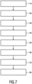
- Fig. 7 shows a principle sketch of a process flow of a method of producing a VCSEL device according to the present invention.
- a substrate substrate 22 in Figs. 1 and 2
- the second part 26 of a second DBR 16 as described above is provided on the substrate 22.
- a light absorption region 20 as described above is provided on the second part 26 of the second DBR 16.
- step 140 third and second regions 32 and 30 of a first part 24 of the second DBR 16 as described above are provided on the light absorption region 20.
- step 150 a contact layer 42 is provided on the second region 30 of the first part 24 of the second DBR 16.
- step 160 a first region 28 of the first part 24 of the second DBR 16 is provided on the second region 30 or the contact layer 42.
- step 160 an active region 14 as described above is provided on the first region 28 of the first part 24 of the second DBR 16.
- the optical resonator 18 comprising the first and second DBRs 12, 16 and the active region 14 is electrically contacted as described above.
- step 180 the photodiode 34 comprising the second and third regions 30, 32 of the first part 24 of the second DBR 16, the light absorption region 20 and the second part 26 of the second DBR 16 is electrically contacted as described above.
- the active region 14 is provided comprising at least one In x Ga 1-x As layer, wherein 0 ⁇ x ⁇ 1, for light emission.
- the light absorption region 20 of the photodiode 34 is provided with at least one In y Ga 1-y As-layer, wherein 0 ⁇ y ⁇ 1, wherein y is greater than x.
- Electrically contacting may comprise one or more steps of etching down the layer structure of the VCSEL device with an appropriate etching technology to the respective layer of the second region 30 of the first part 24 of the second DBR 16 or to the contact layer 42.
- the process may further comprise an oxidation process in order to provide an oxide aperture in the VCSEL of the VCSEL device.
- the production process may further comprise a passivation or planarization process to provide a smooth surface for depositing bond pads.
- the substrate 22 may be removed after depositing the semiconductor layers of the VCSEL structure.
- the n-contact 38 of the photodiode 34 may be provided after thinning or grinding the substrate 22 on the thinned backside of the substrate 22.
- the layers of the first DBR, the active region and any other layers as current injection layers and alike may be deposited by epitaxial methods like MOCVD or MBE.
Landscapes
- Physics & Mathematics (AREA)
- General Physics & Mathematics (AREA)
- Optics & Photonics (AREA)
- Condensed Matter Physics & Semiconductors (AREA)
- Electromagnetism (AREA)
- Engineering & Computer Science (AREA)
- Computer Networks & Wireless Communication (AREA)
- Radar, Positioning & Navigation (AREA)
- Remote Sensing (AREA)
- Semiconductor Lasers (AREA)
Claims (11)
- Vorrichtung mit oberflächenemittierendem Laser mit vertikalem Hohlraum, das einen optischen Resonator (18), eine Fotodiode (34) und eine elektrische Kontaktanordnung (36, 38, 40) umfasst, der optische Resonator (18) einen ersten verteilten Bragg-Reflektor (12), einen zweiten verteilten Bragg-Reflektor (16) und einen aktiven Bereich (14) zur Lichtemission umfasst, wobei der aktive Bereich (14) zwischen dem ersten und dem zweiten verteilten Bragg-Reflektor (12, 16) angeordnet ist, wobei die Fotodiode (34) einen Lichtabsorptionsbereich (20) umfasst, der in dem optischen Resonator (18) angeordnet ist, und die elektrische Kontaktanordnung (36, 38, 40) so angeordnet ist, dass sie einen elektrischen Ansteuerungsstrom bereitstellt, um den optischen Resonator (18) elektrisch zu pumpen und die Fotodiode (34) elektrisch zu kontaktieren, wobei der aktive Bereich (14) mindestens eine InxGa1-xAs-Schicht umfasst, wobei 0 ≤ x < 1, und der Lichtabsorptionsbereich (20) mindestens eine InyGa1-yAs-Schicht umfasst, wobei 0 ≤ y < 1, und wobei y größer als x ist, wobei die InyGa1-yAs-Schicht des Lichtabsorptionsbereichs (20) eine intrinsische Schicht des Lichtabsorptionsbereichs (20) ist, wobeider Lichtabsorptionsbereich (20) der Fotodiode (34) mindestens eine undotierte weitere Schicht umfasst, die auf einem Material basiert, das sich von der InyGa1-yAs-Schicht unterscheidet, wobei die InyGa1-yAs-Schicht unmittelbar an die weitere Schicht angrenzt, undwobei eine intrinsische Zone des Lichtabsorptionsbereichs (20) eine Dicke von mindestens 70 nm aufweist, dadurch gekennzeichnet, dass:- die mindestens eine InyGa1-yAs-Schicht des Lichtabsorptionsbereichs (20) eine Dicke in einem Bereich von 15 nm bis 50 nm aufweist, und- wobei die mindestens eine undotierte weitere Schicht GaAszP1-z' umfasst, mit 0<z<1.
- Vorrichtung mit oberflächenemittierendem Laser mit vertikalem Hohlraum nach Anspruch 1, wobei eine Differenz y - x in einem Bereich von 0,005 bis 0,2, vorzugsweise in einem Bereich von 0,01 bis 0,1, weiter vorzugsweise in einem Bereich von 0,02 bis 0,06 liegt.
- Vorrichtung mit oberflächenemittierendem Laser mit vertikalem Hohlraum nach einem der Ansprüche 1 oder 2, wobei der Lichtabsorptionsbereich (20) der Fotodiode (34) mindestens zwei undotierte weitere Schichten umfasst, wobei die InyGa1-yAs-Schicht durch die weiteren Schichten sandwichartig eingeschlossen ist.
- Vorrichtung mit oberflächenemittierendem Laser mit vertikalem Hohlraum nach einem der Ansprüche 1 bis 3, wobei der Lichtabsorptionsbereich (20) mindestens zwei InyGa1-yAs-Schichten umfasst, die durch mindestens eine undotierte weitere Schicht getrennt sind.
- Vorrichtung mit oberflächenemittierendem Laser mit vertikalem Hohlraum nach einem der Ansprüche 1 bis 4, wobei der Lichtabsorptionsbereich (20) eine einzelne InyGa1-yAs-Schicht umfasst.
- Vorrichtung mit oberflächenemittierendem Laser mit vertikalem Hohlraum nach einem der Ansprüche 1 bis 5, wobei eine intrinsische Zone des Lichtabsorptionsbereichs (20) eine gesamte Dicke von mindestens 100 nm aufweist.
- Vorrichtung mit oberflächenemittierendem Laser mit vertikalem Hohlraum nach einem der Ansprüche 1 bis 5, wobei eine intrinsische Zone des Lichtabsorptionsbereichs (20) eine gesamte Dicke von mindestens 200 nm aufweist.
- Vorrichtung mit oberflächenemittierendem Laser mit vertikalem Hohlraum nach einem der Ansprüche 1 bis 7, wobei die elektrische Kontaktanordnung (36, 38, 40) eine Kontaktschicht (42) umfasst, die zwischen dem aktiven Bereich (14) und dem Lichtabsorptionsbereich (20) im ersten oder zweiten verteilten Bragg-Reflektor (12, 16) angeordnet ist.
- Vorrichtung mit oberflächenemittierendem Laser mit vertikalem Hohlraum nach Anspruch 8, wobei eine optische Dicke der Kontaktschicht (42) ein ganzzahliges Vielfaches der Hälfte der Wellenlänge des Laserlichts in dem optischen Resonator (18) ist.
- Optischer Sensor, der eine Vorrichtung mit oberflächenemittierendem Laser mit vertikalem Hohlraum (10) nach einem der Ansprüche 1 bis 9 umfasst.
- Verfahren zum Herstellen einer Vorrichtung mit oberflächenemittierendem Laser mit vertikalem Hohlraum (10), das Folgendes umfasst:Bereitstellen eines ersten verteilten Bragg-Reflektors (12) und eines zweiten verteilten Bragg-Reflektors (16),Bereitstellen eines aktiven Bereichs (14), der mindestens eine InxGa1-xAs-Schicht für die Lichtemission umfasst, wobei 0 ≤ x < 1, und Anordnen des aktiven Bereichs (14) zwischen dem ersten und dem zweiten verteilten Bragg-Reflektor (12, 16), um einen optischen Resonator (18) zu bilden,Bereitstellen einer Fotodiode (34), die einen Lichtabsorptionsbereich (20) umfasst, der in dem optischen Resonator (18) mit mindestens einer InyGa1-yAs-Schicht angeordnet ist, wobei 0 < y < 1, wobei y größer als x ist,elektrisches Kontaktieren des optischen Resonators (18) undelektrisches Kontaktieren der Fotodiode (34),wobei die InyGa1-yAs-Schicht des Lichtabsorptionsbereichs (20) eine intrinsische Schicht des Lichtabsorptionsbereichs (20) ist,wobei der Lichtabsorptionsbereich (20) der Fotodiode (34) mindestens eine undotierte weitere Schicht umfasst, die auf einem Material basiert, das sich von der InyGa1-yAs-Schicht unterscheidet, wobei die InyGa1-yAs-Schicht unmittelbar an die weitere Schicht angrenzt,und wobei eine intrinsische Zone des Lichtabsorptionsbereichs (20) eine Dicke von mindestens 70 nm aufweist, dadurch gekennzeichnet, dass:- die mindestens eine InyGa1-yAs-Schicht des Lichtabsorptionsbereichs (20) eine Dicke in einem Bereich von 15 nm bis 50 nm aufweist, und- wobei die mindestens eine undotierte weitere Schicht GaAszP1-z umfasst, mit 0<z<1.
Applications Claiming Priority (2)
| Application Number | Priority Date | Filing Date | Title |
|---|---|---|---|
| EP19177927 | 2019-06-03 | ||
| PCT/EP2020/062364 WO2020244862A1 (en) | 2019-06-03 | 2020-05-05 | Vertical cavity surface emitting laser device with monolithically integrated photodiode |
Publications (2)
| Publication Number | Publication Date |
|---|---|
| EP3977574A1 EP3977574A1 (de) | 2022-04-06 |
| EP3977574B1 true EP3977574B1 (de) | 2024-12-04 |
Family
ID=66690271
Family Applications (1)
| Application Number | Title | Priority Date | Filing Date |
|---|---|---|---|
| EP20723128.3A Active EP3977574B1 (de) | 2019-06-03 | 2020-05-05 | Oberflächenemittierende laservorrichtung mit vertikalem resonator mit monolithisch integrierter photodiode |
Country Status (5)
| Country | Link |
|---|---|
| US (1) | US12191630B2 (de) |
| EP (1) | EP3977574B1 (de) |
| KR (1) | KR102630495B1 (de) |
| CN (1) | CN113906641B (de) |
| WO (1) | WO2020244862A1 (de) |
Families Citing this family (4)
| Publication number | Priority date | Publication date | Assignee | Title |
|---|---|---|---|---|
| US20230396037A1 (en) * | 2022-06-03 | 2023-12-07 | Meta Platforms Technologies, Llc | Tunable mems vcsel with embedded photodetector |
| US20240063607A1 (en) * | 2022-08-22 | 2024-02-22 | Ams International Ag | Laser sensor and method of manufacturing a laser sensor |
| JP2026504949A (ja) * | 2023-01-19 | 2026-02-10 | アイリーチ・コーポレーション | パッケージ構造 |
| DE102023102360A1 (de) * | 2023-01-31 | 2024-08-01 | Trumpf Photonic Components Gmbh | VCSEL zum Erzeugen eines Laserlichts |
Family Cites Families (21)
| Publication number | Priority date | Publication date | Assignee | Title |
|---|---|---|---|---|
| US5136603A (en) * | 1991-04-29 | 1992-08-04 | At&T Bell Laboratories | Self-monitoring semiconductor laser device |
| US5475701A (en) * | 1993-12-29 | 1995-12-12 | Honeywell Inc. | Integrated laser power monitor |
| US5606572A (en) * | 1994-03-24 | 1997-02-25 | Vixel Corporation | Integration of laser with photodiode for feedback control |
| US5978401A (en) * | 1995-10-25 | 1999-11-02 | Honeywell Inc. | Monolithic vertical cavity surface emitting laser and resonant cavity photodetector transceiver |
| US5757837A (en) | 1996-10-16 | 1998-05-26 | The Regents Of The University Of California | Intracavity quantum well photodetector integrated within a vertical-cavity surface-emitting laser and method of operating same |
| US6026108A (en) * | 1996-10-16 | 2000-02-15 | The Regents Of The University Of California | Vertical-cavity surface-emitting laser with an intracavity quantum-well optical absorber |
| US5914976A (en) * | 1997-01-08 | 1999-06-22 | W. L. Gore & Associates, Inc. | VCSEL-based multi-wavelength transmitter and receiver modules for serial and parallel optical links |
| US5974071A (en) * | 1997-05-20 | 1999-10-26 | Motorola, Inc. | VCSEL with integrated photodetectors for automatic power control and signal detection in data storage |
| US6055262A (en) | 1997-06-11 | 2000-04-25 | Honeywell Inc. | Resonant reflector for improved optoelectronic device performance and enhanced applicability |
| US5943357A (en) * | 1997-08-18 | 1999-08-24 | Motorola, Inc. | Long wavelength vertical cavity surface emitting laser with photodetector for automatic power control and method of fabrication |
| JP3928295B2 (ja) * | 1999-03-16 | 2007-06-13 | 富士ゼロックス株式会社 | 面発光型半導体レーザ |
| DE10004398A1 (de) | 2000-02-02 | 2001-08-16 | Infineon Technologies Ag | VCSEL mit monolithisch integriertem Photodetektor |
| KR20050019484A (ko) * | 2003-08-19 | 2005-03-03 | 삼성전자주식회사 | 광검출소자가 일체적으로 성장된 장파장 수직 면발광 레이저 |
| KR20050019485A (ko) * | 2003-08-19 | 2005-03-03 | 삼성전자주식회사 | 광검출소자가 일체적으로 형성되는 수직 면발광 레이저 |
| US7746911B2 (en) * | 2004-06-25 | 2010-06-29 | Finisar Corporation | Geometric optimizations for reducing spontaneous emissions in photodiodes |
| US7277463B2 (en) * | 2004-12-30 | 2007-10-02 | Finisar Corporation | Integrated light emitting device and photodiode with ohmic contact |
| US7391800B2 (en) * | 2005-02-02 | 2008-06-24 | Ricoh Company, Ltd. | Vertical cavity surface-emitting semiconductor laser device, optical transmission module, optical transmission device, and optical switching method |
| WO2009136348A1 (en) | 2008-05-09 | 2009-11-12 | Philips Intellectual Property & Standards Gmbh | Vertical cavity surface emitting laser device with monolithically integrated photodiode |
| JP5279393B2 (ja) * | 2008-07-31 | 2013-09-04 | キヤノン株式会社 | 面発光レーザおよびその製造方法、面発光レーザアレイの製造方法、および面発光レーザアレイを備えている光学機器 |
| KR101425480B1 (ko) * | 2012-02-06 | 2014-08-01 | 주식회사 레이칸 | 광모니터링 집적 표면방출레이저 어레이 |
| CN105807378B (zh) * | 2016-05-24 | 2017-07-04 | 北京邮电大学 | 一种收发一体的光电集成芯片 |
-
2020
- 2020-05-05 EP EP20723128.3A patent/EP3977574B1/de active Active
- 2020-05-05 KR KR1020217043151A patent/KR102630495B1/ko active Active
- 2020-05-05 CN CN202080041220.2A patent/CN113906641B/zh active Active
- 2020-05-05 WO PCT/EP2020/062364 patent/WO2020244862A1/en not_active Ceased
-
2021
- 2021-12-01 US US17/539,266 patent/US12191630B2/en active Active
Also Published As
| Publication number | Publication date |
|---|---|
| US12191630B2 (en) | 2025-01-07 |
| CN113906641A (zh) | 2022-01-07 |
| US20220094137A1 (en) | 2022-03-24 |
| KR20220011189A (ko) | 2022-01-27 |
| KR102630495B1 (ko) | 2024-01-29 |
| CN113906641B (zh) | 2024-09-20 |
| WO2020244862A1 (en) | 2020-12-10 |
| EP3977574A1 (de) | 2022-04-06 |
Similar Documents
| Publication | Publication Date | Title |
|---|---|---|
| US8467428B2 (en) | Vertical cavity surface emitting laser device with monolithically integrated photodiode | |
| US12191630B2 (en) | Vertical cavity surface emitting laser device with monolithically integrated photodiode | |
| EP3766150B1 (de) | Vertikalresonator-oberflächenemissionslaservorrichtung mit integriertem tunnelübergang | |
| EP3741014B1 (de) | Vertikalresonator-oberflächenemissionslaservorrichtung mit integrierter fotodiode | |
| US6782027B2 (en) | Resonant reflector for use with optoelectronic devices | |
| US9014225B2 (en) | Vertical cavity surface emitting laser device | |
| US12107388B2 (en) | Vertical cavity surface emitting laser with integrated photodiode | |
| US20250125586A1 (en) | Vertical cavity surface emitting laser device with current-blocking reflector | |
| CN112310809A (zh) | 一种双共振腔vcsel激光器及其制作方法 | |
| WO2017221520A1 (ja) | 半導体発光素子、光通信装置、および半導体発光素子の製造方法 | |
| CN116742475A (zh) | 一种窄线宽垂直腔面发射激光器 | |
| CN117254350A (zh) | 半导体器件及其形成方法 |
Legal Events
| Date | Code | Title | Description |
|---|---|---|---|
| STAA | Information on the status of an ep patent application or granted ep patent |
Free format text: STATUS: UNKNOWN |
|
| STAA | Information on the status of an ep patent application or granted ep patent |
Free format text: STATUS: THE INTERNATIONAL PUBLICATION HAS BEEN MADE |
|
| PUAI | Public reference made under article 153(3) epc to a published international application that has entered the european phase |
Free format text: ORIGINAL CODE: 0009012 |
|
| STAA | Information on the status of an ep patent application or granted ep patent |
Free format text: STATUS: REQUEST FOR EXAMINATION WAS MADE |
|
| 17P | Request for examination filed |
Effective date: 20211215 |
|
| AK | Designated contracting states |
Kind code of ref document: A1 Designated state(s): AL AT BE BG CH CY CZ DE DK EE ES FI FR GB GR HR HU IE IS IT LI LT LU LV MC MK MT NL NO PL PT RO RS SE SI SK SM TR |
|
| DAV | Request for validation of the european patent (deleted) | ||
| DAX | Request for extension of the european patent (deleted) | ||
| GRAP | Despatch of communication of intention to grant a patent |
Free format text: ORIGINAL CODE: EPIDOSNIGR1 |
|
| STAA | Information on the status of an ep patent application or granted ep patent |
Free format text: STATUS: GRANT OF PATENT IS INTENDED |
|
| INTG | Intention to grant announced |
Effective date: 20240626 |
|
| GRAS | Grant fee paid |
Free format text: ORIGINAL CODE: EPIDOSNIGR3 |
|
| GRAA | (expected) grant |
Free format text: ORIGINAL CODE: 0009210 |
|
| STAA | Information on the status of an ep patent application or granted ep patent |
Free format text: STATUS: THE PATENT HAS BEEN GRANTED |
|
| AK | Designated contracting states |
Kind code of ref document: B1 Designated state(s): AL AT BE BG CH CY CZ DE DK EE ES FI FR GB GR HR HU IE IS IT LI LT LU LV MC MK MT NL NO PL PT RO RS SE SI SK SM TR |
|
| REG | Reference to a national code |
Ref country code: CH Ref legal event code: EP |
|
| REG | Reference to a national code |
Ref country code: DE Ref legal event code: R096 Ref document number: 602020042463 Country of ref document: DE |
|
| REG | Reference to a national code |
Ref country code: IE Ref legal event code: FG4D |
|
| REG | Reference to a national code |
Ref country code: LT Ref legal event code: MG9D |
|
| REG | Reference to a national code |
Ref country code: NL Ref legal event code: MP Effective date: 20241204 |
|
| PG25 | Lapsed in a contracting state [announced via postgrant information from national office to epo] |
Ref country code: HR Free format text: LAPSE BECAUSE OF FAILURE TO SUBMIT A TRANSLATION OF THE DESCRIPTION OR TO PAY THE FEE WITHIN THE PRESCRIBED TIME-LIMIT Effective date: 20241204 |
|
| PG25 | Lapsed in a contracting state [announced via postgrant information from national office to epo] |
Ref country code: FI Free format text: LAPSE BECAUSE OF FAILURE TO SUBMIT A TRANSLATION OF THE DESCRIPTION OR TO PAY THE FEE WITHIN THE PRESCRIBED TIME-LIMIT Effective date: 20241204 |
|
| PG25 | Lapsed in a contracting state [announced via postgrant information from national office to epo] |
Ref country code: BG Free format text: LAPSE BECAUSE OF FAILURE TO SUBMIT A TRANSLATION OF THE DESCRIPTION OR TO PAY THE FEE WITHIN THE PRESCRIBED TIME-LIMIT Effective date: 20241204 |
|
| PG25 | Lapsed in a contracting state [announced via postgrant information from national office to epo] |
Ref country code: ES Free format text: LAPSE BECAUSE OF FAILURE TO SUBMIT A TRANSLATION OF THE DESCRIPTION OR TO PAY THE FEE WITHIN THE PRESCRIBED TIME-LIMIT Effective date: 20241204 |
|
| PG25 | Lapsed in a contracting state [announced via postgrant information from national office to epo] |
Ref country code: NO Free format text: LAPSE BECAUSE OF FAILURE TO SUBMIT A TRANSLATION OF THE DESCRIPTION OR TO PAY THE FEE WITHIN THE PRESCRIBED TIME-LIMIT Effective date: 20250304 |
|
| PG25 | Lapsed in a contracting state [announced via postgrant information from national office to epo] |
Ref country code: LV Free format text: LAPSE BECAUSE OF FAILURE TO SUBMIT A TRANSLATION OF THE DESCRIPTION OR TO PAY THE FEE WITHIN THE PRESCRIBED TIME-LIMIT Effective date: 20241204 Ref country code: GR Free format text: LAPSE BECAUSE OF FAILURE TO SUBMIT A TRANSLATION OF THE DESCRIPTION OR TO PAY THE FEE WITHIN THE PRESCRIBED TIME-LIMIT Effective date: 20250305 |
|
| PG25 | Lapsed in a contracting state [announced via postgrant information from national office to epo] |
Ref country code: RS Free format text: LAPSE BECAUSE OF FAILURE TO SUBMIT A TRANSLATION OF THE DESCRIPTION OR TO PAY THE FEE WITHIN THE PRESCRIBED TIME-LIMIT Effective date: 20250304 |
|
| PG25 | Lapsed in a contracting state [announced via postgrant information from national office to epo] |
Ref country code: NL Free format text: LAPSE BECAUSE OF FAILURE TO SUBMIT A TRANSLATION OF THE DESCRIPTION OR TO PAY THE FEE WITHIN THE PRESCRIBED TIME-LIMIT Effective date: 20241204 |
|
| REG | Reference to a national code |
Ref country code: AT Ref legal event code: MK05 Ref document number: 1749183 Country of ref document: AT Kind code of ref document: T Effective date: 20241204 |
|
| PG25 | Lapsed in a contracting state [announced via postgrant information from national office to epo] |
Ref country code: SM Free format text: LAPSE BECAUSE OF FAILURE TO SUBMIT A TRANSLATION OF THE DESCRIPTION OR TO PAY THE FEE WITHIN THE PRESCRIBED TIME-LIMIT Effective date: 20241204 |
|
| PG25 | Lapsed in a contracting state [announced via postgrant information from national office to epo] |
Ref country code: PL Free format text: LAPSE BECAUSE OF FAILURE TO SUBMIT A TRANSLATION OF THE DESCRIPTION OR TO PAY THE FEE WITHIN THE PRESCRIBED TIME-LIMIT Effective date: 20241204 |
|
| PGFP | Annual fee paid to national office [announced via postgrant information from national office to epo] |
Ref country code: DE Payment date: 20250521 Year of fee payment: 6 |
|
| PGFP | Annual fee paid to national office [announced via postgrant information from national office to epo] |
Ref country code: GB Payment date: 20250527 Year of fee payment: 6 |
|
| PG25 | Lapsed in a contracting state [announced via postgrant information from national office to epo] |
Ref country code: IS Free format text: LAPSE BECAUSE OF FAILURE TO SUBMIT A TRANSLATION OF THE DESCRIPTION OR TO PAY THE FEE WITHIN THE PRESCRIBED TIME-LIMIT Effective date: 20250404 |
|
| PG25 | Lapsed in a contracting state [announced via postgrant information from national office to epo] |
Ref country code: PT Free format text: LAPSE BECAUSE OF FAILURE TO SUBMIT A TRANSLATION OF THE DESCRIPTION OR TO PAY THE FEE WITHIN THE PRESCRIBED TIME-LIMIT Effective date: 20250404 |
|
| PG25 | Lapsed in a contracting state [announced via postgrant information from national office to epo] |
Ref country code: EE Free format text: LAPSE BECAUSE OF FAILURE TO SUBMIT A TRANSLATION OF THE DESCRIPTION OR TO PAY THE FEE WITHIN THE PRESCRIBED TIME-LIMIT Effective date: 20241204 |
|
| PGFP | Annual fee paid to national office [announced via postgrant information from national office to epo] |
Ref country code: FR Payment date: 20250528 Year of fee payment: 6 |
|
| PG25 | Lapsed in a contracting state [announced via postgrant information from national office to epo] |
Ref country code: RO Free format text: LAPSE BECAUSE OF FAILURE TO SUBMIT A TRANSLATION OF THE DESCRIPTION OR TO PAY THE FEE WITHIN THE PRESCRIBED TIME-LIMIT Effective date: 20241204 Ref country code: AT Free format text: LAPSE BECAUSE OF FAILURE TO SUBMIT A TRANSLATION OF THE DESCRIPTION OR TO PAY THE FEE WITHIN THE PRESCRIBED TIME-LIMIT Effective date: 20241204 |
|
| PG25 | Lapsed in a contracting state [announced via postgrant information from national office to epo] |
Ref country code: SK Free format text: LAPSE BECAUSE OF FAILURE TO SUBMIT A TRANSLATION OF THE DESCRIPTION OR TO PAY THE FEE WITHIN THE PRESCRIBED TIME-LIMIT Effective date: 20241204 |
|
| PG25 | Lapsed in a contracting state [announced via postgrant information from national office to epo] |
Ref country code: CZ Free format text: LAPSE BECAUSE OF FAILURE TO SUBMIT A TRANSLATION OF THE DESCRIPTION OR TO PAY THE FEE WITHIN THE PRESCRIBED TIME-LIMIT Effective date: 20241204 |
|
| PG25 | Lapsed in a contracting state [announced via postgrant information from national office to epo] |
Ref country code: IT Free format text: LAPSE BECAUSE OF FAILURE TO SUBMIT A TRANSLATION OF THE DESCRIPTION OR TO PAY THE FEE WITHIN THE PRESCRIBED TIME-LIMIT Effective date: 20241204 |
|
| REG | Reference to a national code |
Ref country code: DE Ref legal event code: R097 Ref document number: 602020042463 Country of ref document: DE |
|
| PG25 | Lapsed in a contracting state [announced via postgrant information from national office to epo] |
Ref country code: SE Free format text: LAPSE BECAUSE OF FAILURE TO SUBMIT A TRANSLATION OF THE DESCRIPTION OR TO PAY THE FEE WITHIN THE PRESCRIBED TIME-LIMIT Effective date: 20241204 |
|
| PG25 | Lapsed in a contracting state [announced via postgrant information from national office to epo] |
Ref country code: DK Free format text: LAPSE BECAUSE OF FAILURE TO SUBMIT A TRANSLATION OF THE DESCRIPTION OR TO PAY THE FEE WITHIN THE PRESCRIBED TIME-LIMIT Effective date: 20241204 |
|
| PLBE | No opposition filed within time limit |
Free format text: ORIGINAL CODE: 0009261 |
|
| STAA | Information on the status of an ep patent application or granted ep patent |
Free format text: STATUS: NO OPPOSITION FILED WITHIN TIME LIMIT |
|
| REG | Reference to a national code |
Ref country code: CH Ref legal event code: L10 Free format text: ST27 STATUS EVENT CODE: U-0-0-L10-L00 (AS PROVIDED BY THE NATIONAL OFFICE) Effective date: 20251015 |
|
| 26N | No opposition filed |
Effective date: 20250905 |
|
| REG | Reference to a national code |
Ref country code: CH Ref legal event code: H13 Free format text: ST27 STATUS EVENT CODE: U-0-0-H10-H13 (AS PROVIDED BY THE NATIONAL OFFICE) Effective date: 20251223 |
|
| PG25 | Lapsed in a contracting state [announced via postgrant information from national office to epo] |
Ref country code: LU Free format text: LAPSE BECAUSE OF NON-PAYMENT OF DUE FEES Effective date: 20250505 |
|
| PG25 | Lapsed in a contracting state [announced via postgrant information from national office to epo] |
Ref country code: CH Free format text: LAPSE BECAUSE OF NON-PAYMENT OF DUE FEES Effective date: 20250531 |
|
| REG | Reference to a national code |
Ref country code: BE Ref legal event code: MM Effective date: 20250531 |
|
| PG25 | Lapsed in a contracting state [announced via postgrant information from national office to epo] |
Ref country code: MC Free format text: LAPSE BECAUSE OF FAILURE TO SUBMIT A TRANSLATION OF THE DESCRIPTION OR TO PAY THE FEE WITHIN THE PRESCRIBED TIME-LIMIT Effective date: 20241204 |
|
| PG25 | Lapsed in a contracting state [announced via postgrant information from national office to epo] |
Ref country code: IE Free format text: LAPSE BECAUSE OF NON-PAYMENT OF DUE FEES Effective date: 20250505 |
|
| PG25 | Lapsed in a contracting state [announced via postgrant information from national office to epo] |
Ref country code: BE Free format text: LAPSE BECAUSE OF NON-PAYMENT OF DUE FEES Effective date: 20250531 |