EP3975265A1 - A semiconductor device and a method of manufacturing of a semiconductor device - Google Patents
A semiconductor device and a method of manufacturing of a semiconductor device Download PDFInfo
- Publication number
- EP3975265A1 EP3975265A1 EP20198695.7A EP20198695A EP3975265A1 EP 3975265 A1 EP3975265 A1 EP 3975265A1 EP 20198695 A EP20198695 A EP 20198695A EP 3975265 A1 EP3975265 A1 EP 3975265A1
- Authority
- EP
- European Patent Office
- Prior art keywords
- semiconductor device
- layer
- stack
- nitride
- metal
- Prior art date
- Legal status (The legal status is an assumption and is not a legal conclusion. Google has not performed a legal analysis and makes no representation as to the accuracy of the status listed.)
- Withdrawn
Links
Images

Classifications
-
- H—ELECTRICITY
- H10—SEMICONDUCTOR DEVICES; ELECTRIC SOLID-STATE DEVICES NOT OTHERWISE PROVIDED FOR
- H10D—INORGANIC ELECTRIC SEMICONDUCTOR DEVICES
- H10D8/00—Diodes
- H10D8/60—Schottky-barrier diodes
-
- H—ELECTRICITY
- H10—SEMICONDUCTOR DEVICES; ELECTRIC SOLID-STATE DEVICES NOT OTHERWISE PROVIDED FOR
- H10D—INORGANIC ELECTRIC SEMICONDUCTOR DEVICES
- H10D62/00—Semiconductor bodies, or regions thereof, of devices having potential barriers
- H10D62/10—Shapes, relative sizes or dispositions of the regions of the semiconductor bodies; Shapes of the semiconductor bodies
- H10D62/102—Constructional design considerations for preventing surface leakage or controlling electric field concentration
- H10D62/103—Constructional design considerations for preventing surface leakage or controlling electric field concentration for increasing or controlling the breakdown voltage of reverse-biased devices
- H10D62/105—Constructional design considerations for preventing surface leakage or controlling electric field concentration for increasing or controlling the breakdown voltage of reverse-biased devices by having particular doping profiles, shapes or arrangements of PN junctions; by having supplementary regions, e.g. junction termination extension [JTE]
-
- H—ELECTRICITY
- H10—SEMICONDUCTOR DEVICES; ELECTRIC SOLID-STATE DEVICES NOT OTHERWISE PROVIDED FOR
- H10D—INORGANIC ELECTRIC SEMICONDUCTOR DEVICES
- H10D62/00—Semiconductor bodies, or regions thereof, of devices having potential barriers
- H10D62/10—Shapes, relative sizes or dispositions of the regions of the semiconductor bodies; Shapes of the semiconductor bodies
- H10D62/102—Constructional design considerations for preventing surface leakage or controlling electric field concentration
- H10D62/103—Constructional design considerations for preventing surface leakage or controlling electric field concentration for increasing or controlling the breakdown voltage of reverse-biased devices
- H10D62/105—Constructional design considerations for preventing surface leakage or controlling electric field concentration for increasing or controlling the breakdown voltage of reverse-biased devices by having particular doping profiles, shapes or arrangements of PN junctions; by having supplementary regions, e.g. junction termination extension [JTE]
- H10D62/106—Constructional design considerations for preventing surface leakage or controlling electric field concentration for increasing or controlling the breakdown voltage of reverse-biased devices by having particular doping profiles, shapes or arrangements of PN junctions; by having supplementary regions, e.g. junction termination extension [JTE] having supplementary regions doped oppositely to or in rectifying contact with regions of the semiconductor bodies, e.g. guard rings with PN or Schottky junctions
-
- H—ELECTRICITY
- H10—SEMICONDUCTOR DEVICES; ELECTRIC SOLID-STATE DEVICES NOT OTHERWISE PROVIDED FOR
- H10D—INORGANIC ELECTRIC SEMICONDUCTOR DEVICES
- H10D62/00—Semiconductor bodies, or regions thereof, of devices having potential barriers
- H10D62/80—Semiconductor bodies, or regions thereof, of devices having potential barriers characterised by the materials
- H10D62/83—Semiconductor bodies, or regions thereof, of devices having potential barriers characterised by the materials being Group IV materials, e.g. B-doped Si or undoped Ge
- H10D62/832—Semiconductor bodies, or regions thereof, of devices having potential barriers characterised by the materials being Group IV materials, e.g. B-doped Si or undoped Ge being Group IV materials comprising two or more elements, e.g. SiGe
- H10D62/8325—Silicon carbide
-
- H—ELECTRICITY
- H10—SEMICONDUCTOR DEVICES; ELECTRIC SOLID-STATE DEVICES NOT OTHERWISE PROVIDED FOR
- H10W—GENERIC PACKAGES, INTERCONNECTIONS, CONNECTORS OR OTHER CONSTRUCTIONAL DETAILS OF DEVICES COVERED BY CLASS H10
- H10W74/00—Encapsulations, e.g. protective coatings
- H10W74/10—Encapsulations, e.g. protective coatings characterised by their shape or disposition
- H10W74/131—Encapsulations, e.g. protective coatings characterised by their shape or disposition the semiconductor body being only partially enclosed
- H10W74/137—Encapsulations, e.g. protective coatings characterised by their shape or disposition the semiconductor body being only partially enclosed the encapsulations being directly on the semiconductor body
-
- H—ELECTRICITY
- H10—SEMICONDUCTOR DEVICES; ELECTRIC SOLID-STATE DEVICES NOT OTHERWISE PROVIDED FOR
- H10W—GENERIC PACKAGES, INTERCONNECTIONS, CONNECTORS OR OTHER CONSTRUCTIONAL DETAILS OF DEVICES COVERED BY CLASS H10
- H10W74/00—Encapsulations, e.g. protective coatings
- H10W74/10—Encapsulations, e.g. protective coatings characterised by their shape or disposition
- H10W74/131—Encapsulations, e.g. protective coatings characterised by their shape or disposition the semiconductor body being only partially enclosed
- H10W74/147—Encapsulations, e.g. protective coatings characterised by their shape or disposition the semiconductor body being only partially enclosed the encapsulations being multilayered
-
- H—ELECTRICITY
- H10—SEMICONDUCTOR DEVICES; ELECTRIC SOLID-STATE DEVICES NOT OTHERWISE PROVIDED FOR
- H10W—GENERIC PACKAGES, INTERCONNECTIONS, CONNECTORS OR OTHER CONSTRUCTIONAL DETAILS OF DEVICES COVERED BY CLASS H10
- H10W74/00—Encapsulations, e.g. protective coatings
- H10W74/40—Encapsulations, e.g. protective coatings characterised by their materials
- H10W74/43—Encapsulations, e.g. protective coatings characterised by their materials comprising oxides, nitrides or carbides, e.g. ceramics or glasses
-
- H—ELECTRICITY
- H10—SEMICONDUCTOR DEVICES; ELECTRIC SOLID-STATE DEVICES NOT OTHERWISE PROVIDED FOR
- H10D—INORGANIC ELECTRIC SEMICONDUCTOR DEVICES
- H10D64/00—Electrodes of devices having potential barriers
- H10D64/60—Electrodes characterised by their materials
- H10D64/64—Electrodes comprising a Schottky barrier to a semiconductor
-
- H—ELECTRICITY
- H10—SEMICONDUCTOR DEVICES; ELECTRIC SOLID-STATE DEVICES NOT OTHERWISE PROVIDED FOR
- H10W—GENERIC PACKAGES, INTERCONNECTIONS, CONNECTORS OR OTHER CONSTRUCTIONAL DETAILS OF DEVICES COVERED BY CLASS H10
- H10W72/00—Interconnections or connectors in packages
- H10W72/90—Bond pads, in general
- H10W72/981—Auxiliary members, e.g. spacers
- H10W72/983—Reinforcing structures, e.g. collars
Definitions
- the present invention relates to a semiconductor device with an oxide-nitride-oxide passivation structure.
- the invention also relates to a method of manufacturing a semiconductor device with such an oxide-nitride-oxide passivation structure.
- Semiconductor diodes known in the art require a passivation layer. This passivation layer protects the surface of the semiconductor diodes from a chemical contamination, without disturbing the electrical performance of the semiconductor diode.
- Silicon carbide (SiC) diodes are also known in the art. It is an usual objective in the semiconductor industry to provide smaller, faster, and cheaper semiconductor devices. I.e. improving performance and reducing the semiconductor device cost, while at the same time shrinking packaging size, is fundamental to virtually every semiconductor product type. For power products, improved performance is measured by increased efficiency and power density, higher power handling capability, and wider operating temperature range. Such improvements depend largely on the desirable characteristics of power components used, such as low switching and conduction losses, high switching frequency, stable electrical characteristics over a wide temperature range, high operating temperature, and high blocking voltage. As silicon power semiconductor devices are approaching their theoretical limits, compound semiconductor materials, such as SiC, provide the capability to dramatically improve these parameters.
- SiC devices can deliver significantly better performance.
- the above mentioned passivation layer that protects the surface of the semiconductor diodes from a chemical contamination, without disturbing the electrical performance of the semiconductor diode, is especially important for SiC diodes, because the breakdown voltages and the electric fields of the SiC diodes can be very high.
- silicon nitride can be used as a very efficient diffusion barrier, both for mobile ions and humidity. Silicon nitride provides also a good thermal stability. However, it is a significant disadvantage of silicon nitride that it includes a lot of traps and big amounts of interface charges, which results in destabilizing the border charge balance. Thus, the silicon nitride semiconductor interfaces have very unwanted characteristics.
- Silicon oxide has less traps and charges and it is therefore a preferred interface layer, especially in the proximity of junctions within the semiconductor.
- the significant disadvantage of silicon oxide is that it does not block ions or other chemical contamination, and it does not protect against humidity.
- silicon oxide does not protect from a corrosion caused by humidity and a high voltage exposure.
- a semiconductor device comprises a passivation structure.
- the passivation comprises a first silicon oxide layer, a silicon nitride layer positioned under the first silicon oxide layer, and a second silicon oxide layer positioned under the silicon nitride layer.
- the first silicon oxide layer can be doped with a nitride, which results in an oxi-nitride layer.
- the semiconductor device further comprises a metal contact layer, wherein the passivation structure overlaps an edge of the metal contact layer.
- the metal contact layer is made preferably of Ti, TiN, or TaN, MoN, Pt, Au, Ag, or any other suitable material, or stacks of these materials.
- the top of the metal contact layer in a border region, which border region is in a contact with the environment, is made out of a non-oxidizing metal, e.g. TiN, TaN, MoN, Pt, Au, etc.
- the metal contact layer is made preferably as a layer stack of Ti or any other suitable metal on the bottom of the layer stack, and a metal nitride on the top of the layer stack, wherein the metal nitride is TiN, TaN, MoN or any other suitable metal nitride.
- the semiconductor device as described above provides a termination of SiC high voltage devices to be robust against humidity and charges. This is achieved by a combination of silicon oxide, silicon nitride and silicon oxide layers underneath a polyimide scratch protection, in combination with a Ti/TiN contact layer.
- the second silicon oxide layer makes a reasonable interface to the silicon carbide and ensures sufficient distance of the interface from the traps and charges in the nitride diffusion barrier.
- the first silicon oxide layer secures an excellent adhesion to the scratch protection layer above.
- the remaining exposed TiN layer of the TiN contact layer is robust against corrosion.
- the above described structure of a semiconductor device is especially advantageous for high voltage silicon carbide devices such as Merged-PN-Schottky (MPS) diodes and is combined with a Ti/TiN contact layer.
- MPS Merged-PN-Schottky
- the semiconductor device as described above is designed for a high mechanical robustness and a humidity inertness at the same time.
- a semiconductor device further comprises a polyimide scratch protection structure, wherein the polyimide scratch protection structure is covering the passivation structure.
- the polyimide scratch protection structure is made of 3-20 ⁇ m imide or any other suitable material.
- the semiconductor device further comprises a power metal layer, which power metal layer is for example a low resistance metal layer for electric signal spread.
- the power metal layer can be made of Al, Ag, Cu or any other suitable material or a power metal layer stack comprising two or more of these materials.
- the power metal layer stack can be arranged for soft soldering.
- the top of the power metal layer stack can be:
- the passivation structure is arranged not to cover the power metal layer.
- the passivation structure covers at least partly the top of the power metal layer.
- the first oxide layer of the passivation structure at least partly extends over the top of the top of the power metal layer.
- the semiconductor device further comprises:
- the semiconductor device can be a SiC MPS Schottky diode, a high voltage diode or any other suitable semiconductor device.
- the invention also relates to a method of producing a semiconductor device as described in the above embodiments.
- a semiconductor device comprises a termination, which termination is suitable for SiC high voltage semiconductor devices and which termination is robust against humidity and charges.
- this is achieved by a combination of a first silicon oxide layer, a silicon nitride layer and a second silicon oxide layer, the three layers being positioned underneath a polyimide scratch protection, in a combination with a titanium (Ti) and titanium nitride (TiN) contact layer.
- Ti titanium
- TiN titanium nitride
- it is a Ti/TiN stack, wherein Ti is in contact with a SiC and TiN on the top providing a corrosion protection.
- a semiconductor device provides an excellent protection from humidity, traps and charges. This is achieved by the second silicon oxide layer, which second silicon oxide layer makes a reasonable interface to the silicon carbide and ensures sufficient distance of the interface from the traps and charges in the nitride diffusion barrier.
- the top layer of silicon oxide gives good adhesion to the scratch protection layer above. The remaining exposed TiN layer is robust against corrosion.
- a semiconductor device 10 comprises a oxide-nitride-oxide passivation structure 12a, 12b, 12c.
- the oxide-nitride-oxide passivation structure comprises a first silicon oxide layer 12a, a silicon nitride layer 12b and a second silicon oxide layer 12c. These three layers 12a, 12b, 12c form the passivation structure that is suitable, among other semiconductor devices, for high voltage silicon carbide, or MPS Schottky, diodes.
- the semiconductor device 10 further comprises a Ti/TiN contact layer 14a, 14b.
- the silicon nitride layer is arranged to block ions and humidity.
- the silicon nitride is full of traps and for this reason has to be relatively thin, so that the charge in proximity of the termination is reduced.
- said silicon nitride is preferably kept away from the silicon carbide (SiC) in order to decouple the SiC surface from the traps and charges, thereby lowering the impact of the charge.
- the first silicon oxide layer provides an increased adhesion to a polyimide.
- a termination design of the semiconductor device comprises the oxide-nitride-oxide passivation structure 12a, 12b, 12c and a Ti/TiN contact layer 14a, 14b.
- the oxide-nitride-oxide passivation structure 12a, 12b, 12c is covered by a polyimide scratch protection 26.
- the oxide-nitride-oxide passivation structure 12a, 12b, 12c overlaps the edge of the Ti/TiN contact layer 14a, 14b and the edge of a termination layer 16, i.e. a p-border termination 16.
- the oxide-nitride-oxide passivation structure 12a, 12b, 12c is arranged so not to cover a soft power metal layer 22. Such an arrangement secures that no passivation cracks form under thermo and/or mechanical stress.
- the soft power metal layer 22 can be made of Al, Ag, Cu or any other suitable material.
- the second oxide layer 12c makes a reasonable interface to the silicon carbide and ensures sufficient distance of the SiC surface interface from the traps and charges in the nitride.
- the thickness of this second oxide layer 12c is crucial to minimize the impact of silicon nitride bulk and interface charges.
- the silicon nitride layer 12b serves as a good diffusion barrier.
- the first silicon oxide layer 12a secures a good adhesion to the layer above the first silicon oxide layer 12a.
- the layer above is the polyimide scratch protection 26.
- the polyimide scratch protection 26 can be made of 3-20 ⁇ m imide.
- the Ti/TiN contact layer 14a, 14b is preferably relatively thin and this layer is resistant against corrosion since its top surface 14a is formed by TiN, which does not corrode under humidity and high voltage conditions.
- alternative non-oxidizing top contact metals 14a could be TaN, MoN, Pt, Au, Ag etc.
- the Ti/TiN contact layer 14a, 14b is made preferably of a layer stack of Ti on the bottom of the layer stack 14b and a metal nitride on the top of the layer stack 14a, wherein the metal nitride is TiN, TaN, MoN or any other suitable metal nitride.
- the semiconductor device further comprises a p-well 17, a p-plus contact 18, an epi 20 and a substrate 24 as shown in Figure 1 .
- a semiconductor device 40 comprises an oxide-nitride-oxide passivation structure 46 on top of a power metal contact layer 50.
- the power contact layer 50 can be a Ti/TiN contact.
- the advantage of such arrangement of the oxide-nitride-oxide passivation structure 46 in respect to the power contact layer 50 is securing the best adhesion to a polyimide scratch protection 44.
- Such a design of the semiconductor device 40 is suitable for module packages with gel coating, where the thermo-mechanic stress to the oxide-nitride-oxide passivation structure 46 is much lower.
- the semiconductor device 40 comprises:
- the oxide-nitride-oxide passivation structure 46a, 46b, 46c comprises a first silicon oxide layer 46a, a silicon nitride layer 46b below the first oxide layer 46a and a second silicon oxide layer 46c below the silicon nitride layer 46b.
- a semiconductor device 80 comprises an oxide-nitride-oxide passivation structure.
- the oxide-nitride-oxide passivation structure comprises a first silicon oxide layer 90, a silicon nitride layer 92 partly under the first silicon oxide layer 90 and a second silicon oxide layer 94 under the silicon nitride layer 92.
- the semiconductor device further comprises a power metal contact layer 88a, 88b (e.g. a Ti/TiN contact layer 88a, 88b), a power metal layer 86, and a polyimide scratch protection 82.
- the first oxide layer 90 is extended to the top of the metal layer 86. This preferred embodiment secures a good adhesion and a lower risk of passivation cracks.
- the semiconductor device further comprises a p-border termination 95, a p-well 96, a p-plus contact 97, an epi 98 and a substrate 99 as shown in Figure 3 .
- the termination design comprises the oxide-nitride-oxide passivation structure to form the advantageous passivation layer stack in combination with a robust Ti/TiN contact layer.
- the overlap of full passivation stack and power metal is avoided.
- only the thin first oxide layer 90 is in contact with the power metal layer 86, which makes the semiconductor device robust against high-stress environments, as required in moulded packages, and high humidity environments, as required for gel-coated modules.
- a high mechanical robustness and a humidity inertness are achieved.
- the invention is applicable for various semiconductor devices, especially for SiC MPS Schottky diodes, and/or any kind of high voltage diodes and other semiconductor devices.
Landscapes
- Electrodes Of Semiconductors (AREA)
Abstract
This disclosure relates to a semiconductor device comprising a passivation structure, wherein the passivation comprises a first silicon oxide layer, a silicon nitride layer positioned under the first silicon oxide layer, and a second silicon oxide layer positioned under the silicon nitride layer. The semiconductor device further comprises a metal contact layer, wherein the passivation structure overlaps an edge of the metal contact layer. The metal contact layer can be a Ti/TiN contact layer.
Description
- The present invention relates to a semiconductor device with an oxide-nitride-oxide passivation structure. The invention also relates to a method of manufacturing a semiconductor device with such an oxide-nitride-oxide passivation structure.
- Semiconductor diodes known in the art require a passivation layer. This passivation layer protects the surface of the semiconductor diodes from a chemical contamination, without disturbing the electrical performance of the semiconductor diode.
- Silicon carbide (SiC) diodes are also known in the art. It is an usual objective in the semiconductor industry to provide smaller, faster, and cheaper semiconductor devices. I.e. improving performance and reducing the semiconductor device cost, while at the same time shrinking packaging size, is fundamental to virtually every semiconductor product type. For power products, improved performance is measured by increased efficiency and power density, higher power handling capability, and wider operating temperature range. Such improvements depend largely on the desirable characteristics of power components used, such as low switching and conduction losses, high switching frequency, stable electrical characteristics over a wide temperature range, high operating temperature, and high blocking voltage. As silicon power semiconductor devices are approaching their theoretical limits, compound semiconductor materials, such as SiC, provide the capability to dramatically improve these parameters.
- Although silicon power products continue provide some incremental improvements, SiC devices can deliver significantly better performance.
- The above mentioned passivation layer, that protects the surface of the semiconductor diodes from a chemical contamination, without disturbing the electrical performance of the semiconductor diode, is especially important for SiC diodes, because the breakdown voltages and the electric fields of the SiC diodes can be very high.
- It is known in the art that silicon nitride can be used as a very efficient diffusion barrier, both for mobile ions and humidity. Silicon nitride provides also a good thermal stability. However, it is a significant disadvantage of silicon nitride that it includes a lot of traps and big amounts of interface charges, which results in destabilizing the border charge balance. Thus, the silicon nitride semiconductor interfaces have very unwanted characteristics.
- Another drawback of the silicon nitride semiconductor devices is that for other materials adhesion to silicon nitride is low. This causes problems when additional layers must be used either for passivation or for other purposes.
- Silicon oxide has less traps and charges and it is therefore a preferred interface layer, especially in the proximity of junctions within the semiconductor. However, the significant disadvantage of silicon oxide is that it does not block ions or other chemical contamination, and it does not protect against humidity.
- Moreover, silicon oxide does not protect from a corrosion caused by humidity and a high voltage exposure.
- Various example embodiments are directed to the disadvantage as described above and/or others which may become apparent from the following disclosure.
- According to an embodiment of this invention a semiconductor device comprises a passivation structure. The passivation comprises a first silicon oxide layer, a silicon nitride layer positioned under the first silicon oxide layer, and a second silicon oxide layer positioned under the silicon nitride layer.
- The first silicon oxide layer can be doped with a nitride, which results in an oxi-nitride layer.
- The semiconductor device further comprises a metal contact layer, wherein the passivation structure overlaps an edge of the metal contact layer.
- The metal contact layer is made preferably of Ti, TiN, or TaN, MoN, Pt, Au, Ag, or any other suitable material, or stacks of these materials. The top of the metal contact layer in a border region, which border region is in a contact with the environment, is made out of a non-oxidizing metal, e.g. TiN, TaN, MoN, Pt, Au, etc.
- The metal contact layer is made preferably as a layer stack of Ti or any other suitable metal on the bottom of the layer stack, and a metal nitride on the top of the layer stack, wherein the metal nitride is TiN, TaN, MoN or any other suitable metal nitride.
- The semiconductor device as described above provides a termination of SiC high voltage devices to be robust against humidity and charges. This is achieved by a combination of silicon oxide, silicon nitride and silicon oxide layers underneath a polyimide scratch protection, in combination with a Ti/TiN contact layer.
- The second silicon oxide layer makes a reasonable interface to the silicon carbide and ensures sufficient distance of the interface from the traps and charges in the nitride diffusion barrier. The first silicon oxide layer secures an excellent adhesion to the scratch protection layer above. The remaining exposed TiN layer of the TiN contact layer is robust against corrosion.
- The above described structure of a semiconductor device is especially advantageous for high voltage silicon carbide devices such as Merged-PN-Schottky (MPS) diodes and is combined with a Ti/TiN contact layer.
- Moreover, the overlap of passivation and power metal is avoided. This makes the semiconductor device design robust against high-stress environments, e.g. for moulded packages.
- Thus, the semiconductor device as described above is designed for a high mechanical robustness and a humidity inertness at the same time.
- According to an embodiment of the invention, a semiconductor device further comprises a polyimide scratch protection structure, wherein the polyimide scratch protection structure is covering the passivation structure.
- The polyimide scratch protection structure is made of 3-20 µm imide or any other suitable material.
- The semiconductor device further comprises a power metal layer, which power metal layer is for example a low resistance metal layer for electric signal spread. The power metal layer can be made of Al, Ag, Cu or any other suitable material or a power metal layer stack comprising two or more of these materials.
- The power metal layer stack can be arranged for soft soldering. The top of the power metal layer stack can be:
- Ni, Cu; or Ag;
- a stack of Ni and Ag;
- a stack of Ti and Ni;
- a stack of Cu and Sn;
- a stack of Ti and NiV;
- a stack of Ti, Ni and Ag; or
- a stack of Ti, NiV and Ag.
- According to an embodiment of the invention the passivation structure is arranged not to cover the power metal layer.
- According to another embodiment of the invention the passivation structure covers at least partly the top of the power metal layer.
- According to an embodiment of the invention the first oxide layer of the passivation structure at least partly extends over the top of the top of the power metal layer.
- The semiconductor device further comprises:
- a substrate,
- an epi, positioned on the substrate,
- a p-border termination,
- a p-well, and
- a p-plus contact on the top of the p-well.
- The semiconductor device can be a SiC MPS Schottky diode, a high voltage diode or any other suitable semiconductor device.
- The invention also relates to a method of producing a semiconductor device as described in the above embodiments.
- So that the manner in which the features of the present disclosure can be understood in detail, a more particular description is made with reference to embodiments, some of which are illustrated in the appended figures. It is to be noted, however, that the appended figures illustrate only typical embodiments and are therefore not to be considered limiting of its scope. The figures are for facilitating an understanding of the disclosure and thus are not necessarily drawn to scale. Advantages of the subject matter claimed will become apparent to those skilled in the art upon reading this description in conjunction with the accompanying figures, in which like reference numerals have been used to designate like elements, and in which:
-
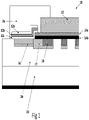
Figure 1 illustrates a semiconductor device according to an embodiment of the invention; -
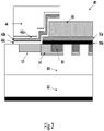
Figure 2 illustrates a semiconductor device according to another embodiment of the invention; -
Figure 3 illustrates a semiconductor device according to another embodiment of the invention; - According to an embodiment of the invention, a semiconductor device comprises a termination, which termination is suitable for SiC high voltage semiconductor devices and which termination is robust against humidity and charges. According to an embodiment of the invention, this is achieved by a combination of a first silicon oxide layer, a silicon nitride layer and a second silicon oxide layer, the three layers being positioned underneath a polyimide scratch protection, in a combination with a titanium (Ti) and titanium nitride (TiN) contact layer. In a preferred embodiment it is a Ti/TiN stack, wherein Ti is in contact with a SiC and TiN on the top providing a corrosion protection.
- A semiconductor device according to above embodiment provides an excellent protection from humidity, traps and charges. This is achieved by the second silicon oxide layer, which second silicon oxide layer makes a reasonable interface to the silicon carbide and ensures sufficient distance of the interface from the traps and charges in the nitride diffusion barrier. The top layer of silicon oxide gives good adhesion to the scratch protection layer above. The remaining exposed TiN layer is robust against corrosion.
- An embodiment of the invention is shown in
Figure 1 . Asemiconductor device 10 comprises a oxide-nitride-oxide passivation structure silicon oxide layer 12a, asilicon nitride layer 12b and a second silicon oxide layer 12c. These threelayers semiconductor device 10 further comprises a Ti/TiN contact layer - The silicon nitride layer is arranged to block ions and humidity. The silicon nitride is full of traps and for this reason has to be relatively thin, so that the charge in proximity of the termination is reduced.
- Moreover, said silicon nitride is preferably kept away from the silicon carbide (SiC) in order to decouple the SiC surface from the traps and charges, thereby lowering the impact of the charge.
- The first silicon oxide layer provides an increased adhesion to a polyimide.
- As shown in
Figure 1 , a termination design of the semiconductor device comprises the oxide-nitride-oxide passivation structure TiN contact layer oxide passivation structure polyimide scratch protection 26. - The oxide-nitride-
oxide passivation structure TiN contact layer termination layer 16, i.e. a p-border termination 16. The oxide-nitride-oxide passivation structure power metal layer 22. Such an arrangement secures that no passivation cracks form under thermo and/or mechanical stress. The softpower metal layer 22 can be made of Al, Ag, Cu or any other suitable material. - The second oxide layer 12c makes a reasonable interface to the silicon carbide and ensures sufficient distance of the SiC surface interface from the traps and charges in the nitride. The thickness of this second oxide layer 12c is crucial to minimize the impact of silicon nitride bulk and interface charges.
- The
silicon nitride layer 12b serves as a good diffusion barrier. - The first
silicon oxide layer 12a secures a good adhesion to the layer above the firstsilicon oxide layer 12a. In this exemplary embodiment the layer above is thepolyimide scratch protection 26. Thepolyimide scratch protection 26 can be made of 3-20 µm imide. - The Ti/
TiN contact layer top surface 14a is formed by TiN, which does not corrode under humidity and high voltage conditions. In another embodiment of the present invention alternative non-oxidizingtop contact metals 14a could be TaN, MoN, Pt, Au, Ag etc. - The Ti/
TiN contact layer layer stack 14b and a metal nitride on the top of thelayer stack 14a, wherein the metal nitride is TiN, TaN, MoN or any other suitable metal nitride. - The semiconductor device further comprises a p-
well 17, a p-plus contact 18, anepi 20 and asubstrate 24 as shown inFigure 1 . - An embodiment of the invention is shown in
Figure 2 . Asemiconductor device 40 comprises an oxide-nitride-oxide passivation structure 46 on top of a power metal contact layer 50. The power contact layer 50 can be a Ti/TiN contact. The advantage of such arrangement of the oxide-nitride-oxide passivation structure 46 in respect to the power contact layer 50 is securing the best adhesion to apolyimide scratch protection 44. Such a design of thesemiconductor device 40 is suitable for module packages with gel coating, where the thermo-mechanic stress to the oxide-nitride-oxide passivation structure 46 is much lower. - According to the example embodiment shown in
Figure 2 , thesemiconductor device 40 comprises: - a
substrate 62, - an
epi 60, positioned on thesubstrate 62, - a p-
border termination 52, - a p-
well 54, - a p-
plus contact 56 on the top of the p-well 54, - a power
metal contact layer TiN contact - an Al
power metal layer 48, on the top of the powermetal contact layer - an oxide-nitride-
oxide passivation structure metal contact layer power metal layer 48, and - a
polyimide scratch protection 44 on the top of the oxide-nitride-oxide passivation structure - The oxide-nitride-
oxide passivation structure silicon oxide layer 46a, asilicon nitride layer 46b below thefirst oxide layer 46a and a secondsilicon oxide layer 46c below thesilicon nitride layer 46b. - An embodiment of the invention is shown in
Figure 3 . Asemiconductor device 80 comprises an oxide-nitride-oxide passivation structure. The oxide-nitride-oxide passivation structure comprises a firstsilicon oxide layer 90, asilicon nitride layer 92 partly under the firstsilicon oxide layer 90 and a secondsilicon oxide layer 94 under thesilicon nitride layer 92. The semiconductor device further comprises a powermetal contact layer TiN contact layer power metal layer 86, and apolyimide scratch protection 82. - In this embodiment of the invention the
first oxide layer 90 is extended to the top of themetal layer 86. This preferred embodiment secures a good adhesion and a lower risk of passivation cracks. - The semiconductor device further comprises a p-
border termination 95, a p-well 96, a p-plus contact 97, anepi 98 and asubstrate 99 as shown inFigure 3 . - The advantage of the above presented embodiments of the invention is that the termination design comprises the oxide-nitride-oxide passivation structure to form the advantageous passivation layer stack in combination with a robust Ti/TiN contact layer. By such an arrangement the overlap of full passivation stack and power metal is avoided. Instead, only the thin
first oxide layer 90 is in contact with thepower metal layer 86, which makes the semiconductor device robust against high-stress environments, as required in moulded packages, and high humidity environments, as required for gel-coated modules. Thus, at the same time a high mechanical robustness and a humidity inertness are achieved. - The invention is applicable for various semiconductor devices, especially for SiC MPS Schottky diodes, and/or any kind of high voltage diodes and other semiconductor devices.
- Particular and preferred aspects of the invention are set out in the accompanying independent claims. Combinations of features from the dependent and/or independent claims may be combined as appropriate and not merely as set out in the claims.
- The scope of the present disclosure includes any novel feature or combination of features disclosed therein either explicitly or implicitly or any generalisation thereof irrespective of whether or not it relates to the claimed invention or mitigate against any or all of the problems addressed by the present invention. The applicant hereby gives notice that new claims may be formulated to such features during prosecution of this application or of any such further application derived therefrom. In particular, with reference to the appended claims, features from dependent claims may be combined with those of the independent claims and features from respective independent claims may be combined in any appropriate manner and not merely in specific combinations enumerated in the claims.
- Features which are described in the context of separate embodiments may also be provided in combination in a single embodiment. Conversely, various features which are, for brevity, described in the context of a single embodiment, may also be provided separately or in any suitable sub combination.
- Term "comprising" does not exclude other elements or steps, the term "a" or "an" does not exclude a plurality. Reference signs in the claims shall not be construed as limiting the scope of the claims.
Claims (16)
- A semiconductor device comprising a passivation structure, wherein the passivation comprises:- a first silicon oxide layer,- a silicon nitride layer positioned under the first silicon oxide layer, and- a second silicon oxide layer positioned under the silicon nitride layer.
- A semiconductor device as claimed in claim 1, wherein the first silicon oxide layer is doped with a nitride.
- A semiconductor device as claimed in claims 1 or 2, wherein the semiconductor device further comprises a metal contact layer, wherein the passivation structure overlaps an edge of the metal contact layer.
- A semiconductor device as claimed in claim 3, wherein the metal contact layer is made preferably of Ti, TiN, or TaN, MoN, Pt, Au, Ag, or any other suitable material, or stacks of these materials.
- A semiconductor device as claimed in claims 3 or 4, wherein the metal contact layer is preferably a layer stack comprising Ti or any other suitable metal on the bottom of the layer stack, and a metal nitride on the top of the layer stack, wherein the metal nitride is TiN, TaN, MoN or any other suitable metal nitride.
- A semiconductor device as claimed in any of the previous claims, wherein the semiconductor device further comprises a polyimide scratch protection structure, wherein the polyimide scratch protection structure is covering the passivation structure.
- A semiconductor device as claimed in claim 6, wherein the polyimide scratch protection structure is made of 3-20 µm imide or any other suitable material.
- A semiconductor device as claimed in any of the previous claims, wherein the semiconductor device further comprises a power metal layer.
- A semiconductor device as claimed in claim 8, wherein the power metal layer is made of Al, Ag, Cu or any other suitable material, or a power metal layer stack comprising two or more of these materials.
- A semiconductor device as claimed in claim 9, wherein the power metal layer stack is arranged for soft soldering, wherein the top of the power metal layer stack is:- Ni, Cu; or Ag;- a stack of Ni and Ag;- a stack of Ti and Ni;- a stack of Cu and Sn;- a stack of Ti and NiV;- a stack of Ti, Ni and Ag; or- a stack of Ti, NiV and Ag.
- A semiconductor device as claimed in claims 8, 9 or 10, wherein the passivation structure is arranged not to cover the power metal layer.
- A semiconductor device as claimed in claims 8, 9 or 10, wherein the passivation structure covers at least partly the top of the power metal layer.
- A semiconductor device as claimed in claims 8, 9 or 10, wherein the first oxide layer of the passivation structure at least partly extends over the top of the top of the power metal layer.
- A semiconductor device as claimed in any of the previous claims, wherein the semiconductor device further comprises:- a substrate,- an epi, positioned on the substrate,- a p-border termination,- a p-well, and- a p-plus contact on the top of the p-well.
- A semiconductor device as claimed in any of the previous claims, wherein the semiconductor device is a SiC MPS Schottky diode, a high voltage diode or any other suitable semiconductor device.
- A method of producing a semiconductor device as claimed in any of the previous claims.
Priority Applications (1)
| Application Number | Priority Date | Filing Date | Title |
|---|---|---|---|
| EP20198695.7A EP3975265A1 (en) | 2020-09-28 | 2020-09-28 | A semiconductor device and a method of manufacturing of a semiconductor device |
Applications Claiming Priority (1)
| Application Number | Priority Date | Filing Date | Title |
|---|---|---|---|
| EP20198695.7A EP3975265A1 (en) | 2020-09-28 | 2020-09-28 | A semiconductor device and a method of manufacturing of a semiconductor device |
Publications (1)
| Publication Number | Publication Date |
|---|---|
| EP3975265A1 true EP3975265A1 (en) | 2022-03-30 |
Family
ID=72670491
Family Applications (1)
| Application Number | Title | Priority Date | Filing Date |
|---|---|---|---|
| EP20198695.7A Withdrawn EP3975265A1 (en) | 2020-09-28 | 2020-09-28 | A semiconductor device and a method of manufacturing of a semiconductor device |
Country Status (1)
| Country | Link |
|---|---|
| EP (1) | EP3975265A1 (en) |
Cited By (3)
| Publication number | Priority date | Publication date | Assignee | Title |
|---|---|---|---|---|
| EP4386829A3 (en) * | 2022-11-25 | 2024-08-21 | STMicroelectronics International N.V. | Sic-based electronic device with multilayer and multifunctional passivation, and method of manufacturing the electronic device |
| WO2025161818A1 (en) * | 2024-02-01 | 2025-08-07 | 华为技术有限公司 | Semiconductor device and manufacturing method therefor, chip, electronic device, and vehicle |
| DE102024203635A1 (en) * | 2024-04-18 | 2025-10-23 | Infineon Technologies Ag | SEMICONDUCTOR CHIP AND METHOD FOR MANUFACTURING THE SAME |
Citations (7)
| Publication number | Priority date | Publication date | Assignee | Title |
|---|---|---|---|---|
| US20120115319A1 (en) * | 2010-11-10 | 2012-05-10 | Cree, Inc. | Contact pad |
| US9391136B1 (en) * | 2015-03-24 | 2016-07-12 | Sanken Electric Co., Ltd. | Semiconductor device |
| US20180040563A1 (en) * | 2015-03-27 | 2018-02-08 | Mitsubishi Electric Corporation | Semiconductor device and method for manufacturing same |
| US9991399B2 (en) * | 2012-10-04 | 2018-06-05 | Cree, Inc. | Passivation structure for semiconductor devices |
| US10020373B1 (en) * | 2017-02-22 | 2018-07-10 | Sanken Electric Co., Ltd. | Semiconductor device |
| US20190165159A1 (en) * | 2017-11-24 | 2019-05-30 | Infineon Technologies Ag | Silicon Carbide Semiconductor Component with Edge Termination Structure |
| US20190311966A1 (en) * | 2018-04-10 | 2019-10-10 | Infineon Technologies Ag | Semiconductor Device and Method for Forming a Semiconductor Device |
-
2020
- 2020-09-28 EP EP20198695.7A patent/EP3975265A1/en not_active Withdrawn
Patent Citations (7)
| Publication number | Priority date | Publication date | Assignee | Title |
|---|---|---|---|---|
| US20120115319A1 (en) * | 2010-11-10 | 2012-05-10 | Cree, Inc. | Contact pad |
| US9991399B2 (en) * | 2012-10-04 | 2018-06-05 | Cree, Inc. | Passivation structure for semiconductor devices |
| US9391136B1 (en) * | 2015-03-24 | 2016-07-12 | Sanken Electric Co., Ltd. | Semiconductor device |
| US20180040563A1 (en) * | 2015-03-27 | 2018-02-08 | Mitsubishi Electric Corporation | Semiconductor device and method for manufacturing same |
| US10020373B1 (en) * | 2017-02-22 | 2018-07-10 | Sanken Electric Co., Ltd. | Semiconductor device |
| US20190165159A1 (en) * | 2017-11-24 | 2019-05-30 | Infineon Technologies Ag | Silicon Carbide Semiconductor Component with Edge Termination Structure |
| US20190311966A1 (en) * | 2018-04-10 | 2019-10-10 | Infineon Technologies Ag | Semiconductor Device and Method for Forming a Semiconductor Device |
Non-Patent Citations (2)
| Title |
|---|
| FUJINO YUHKI ET AL: "Novel Manufacturing Process for Si Superjunction Power MOSFETs with Air-Gap and Insulating Cap Layer", 2019 JOINT INTERNATIONAL SYMPOSIUM ON E-MANUFACTURING & DESIGN COLLABORATION(EMDC) & SEMICONDUCTOR MANUFACTURING (ISSM), TAIWAN SEMICONDUCTOR INDUSTRY ASSOCIATION, 6 September 2019 (2019-09-06), pages 1 - 4, XP033753047, DOI: 10.23919/EMDC/ISSM48219.2019.9052133 * |
| NOT PROCESSED, THE COMPILED STATE-OF-THE-ART OF PV SOLAR TECHNOLOGY AND DEPLOYMENT : 22ND EUROPEAN PHOTOVOLTAIC SOLAR ENERGY CONFERENCE, EU PVSEC ; PROCEEDINGS OF THE INTERNATIONAL CONFERENCE, HELD IN MILAN, ITALY, 3 - 7 SEPTEMBER 2007, MUNICH : WIP-RENEWABLE ENERG, 3 September 2007 (2007-09-03), XP040513304, ISBN: 978-3-936338-22-5 * |
Cited By (5)
| Publication number | Priority date | Publication date | Assignee | Title |
|---|---|---|---|---|
| EP4386829A3 (en) * | 2022-11-25 | 2024-08-21 | STMicroelectronics International N.V. | Sic-based electronic device with multilayer and multifunctional passivation, and method of manufacturing the electronic device |
| EP4451323A3 (en) * | 2022-11-25 | 2025-01-08 | STMicroelectronics International N.V. | Sic-based electronic device with multilayer and multifunctional passivation, and method of manufacturing the electronic device |
| EP4521456A3 (en) * | 2022-11-25 | 2025-05-14 | STMicroelectronics International N.V. | Sic-based electronic device with multilayer and multifunctional passivation, and method of manufacturing the electronic device |
| WO2025161818A1 (en) * | 2024-02-01 | 2025-08-07 | 华为技术有限公司 | Semiconductor device and manufacturing method therefor, chip, electronic device, and vehicle |
| DE102024203635A1 (en) * | 2024-04-18 | 2025-10-23 | Infineon Technologies Ag | SEMICONDUCTOR CHIP AND METHOD FOR MANUFACTURING THE SAME |
Similar Documents
| Publication | Publication Date | Title |
|---|---|---|
| KR100632137B1 (en) | Semiconductor device assembly, half bridge drive circuit, solenoid drive circuit, full bridge drive circuit, and voltage level converter circuit | |
| US11367683B2 (en) | Silicon carbide device and method for forming a silicon carbide device | |
| US10020373B1 (en) | Semiconductor device | |
| EP3285290B1 (en) | Power semiconductor device and method for manufacturing such a power semiconductor device | |
| US11164813B2 (en) | Transistor semiconductor die with increased active area | |
| EP4084064B1 (en) | Semiconductor device | |
| KR100750696B1 (en) | Chip-scale schottky device | |
| EP3635780B1 (en) | Silicon carbide power module | |
| CN113678261A (en) | Semiconductor device and semiconductor module | |
| WO2022066696A1 (en) | Edge termination structures for semiconductor devices | |
| EP3279935A1 (en) | Power semiconductor module | |
| CN105765723A (en) | Optoelectronic semiconductor chip with built-in ESD protection | |
| EP1902466A2 (en) | Schottky diode with improved surge capability | |
| CN121058363A (en) | Power semiconductor devices and methods for manufacturing power semiconductor devices | |
| US10546795B2 (en) | Power semiconductor device and method for producing a power semiconductor device | |
| EP0518605B1 (en) | Bi-directional surge suppressor circuit | |
| CN107293533A (en) | Transient Voltage Suppressor and its manufacture method | |
| EP4386829A2 (en) | Sic-based electronic device with multilayer and multifunctional passivation, and method of manufacturing the electronic device | |
| EP3686924A1 (en) | Group iii-nitride based vertical power device and system | |
| US11869840B2 (en) | Silicon carbide device and method for forming a silicon carbide device | |
| CN107301996A (en) | Transient Voltage Suppressor and its manufacture method | |
| EP2092561B1 (en) | Bond pad structure and method for producing same | |
| EP4668328A1 (en) | Sic-based electronic device with enhanced robustness and method for manufacturing the electronic device | |
| US20250343091A1 (en) | Integration of Liner in Passivation Stack | |
| US12080762B2 (en) | Silicon carbide semiconductor device and method of manufacturing silicon carbide semiconductor device |
Legal Events
| Date | Code | Title | Description |
|---|---|---|---|
| PUAI | Public reference made under article 153(3) epc to a published international application that has entered the european phase |
Free format text: ORIGINAL CODE: 0009012 |
|
| STAA | Information on the status of an ep patent application or granted ep patent |
Free format text: STATUS: THE APPLICATION HAS BEEN PUBLISHED |
|
| AK | Designated contracting states |
Kind code of ref document: A1 Designated state(s): AL AT BE BG CH CY CZ DE DK EE ES FI FR GB GR HR HU IE IS IT LI LT LU LV MC MK MT NL NO PL PT RO RS SE SI SK SM TR |
|
| STAA | Information on the status of an ep patent application or granted ep patent |
Free format text: STATUS: THE APPLICATION IS DEEMED TO BE WITHDRAWN |
|
| 18D | Application deemed to be withdrawn |
Effective date: 20221001 |