EP3975188B1 - Electric field shielding apparatus that does not affect transmission efficiency of wirelessly coupled transmission coil - Google Patents
Electric field shielding apparatus that does not affect transmission efficiency of wirelessly coupled transmission coil Download PDFInfo
- Publication number
- EP3975188B1 EP3975188B1 EP19935741.9A EP19935741A EP3975188B1 EP 3975188 B1 EP3975188 B1 EP 3975188B1 EP 19935741 A EP19935741 A EP 19935741A EP 3975188 B1 EP3975188 B1 EP 3975188B1
- Authority
- EP
- European Patent Office
- Prior art keywords
- transmission coil
- annular metal
- semi
- electric field
- shielding apparatus
- Prior art date
- Legal status (The legal status is an assumption and is not a legal conclusion. Google has not performed a legal analysis and makes no representation as to the accuracy of the status listed.)
- Active
Links
- 230000005540 biological transmission Effects 0.000 title claims description 68
- 230000005684 electric field Effects 0.000 title claims description 30
- 239000002184 metal Substances 0.000 claims description 29
- 229910052751 metal Inorganic materials 0.000 claims description 29
- 230000008878 coupling Effects 0.000 claims description 3
- 238000010168 coupling process Methods 0.000 claims description 3
- 238000005859 coupling reaction Methods 0.000 claims description 3
- RYGMFSIKBFXOCR-UHFFFAOYSA-N Copper Chemical compound [Cu] RYGMFSIKBFXOCR-UHFFFAOYSA-N 0.000 claims description 2
- 229910052802 copper Inorganic materials 0.000 claims description 2
- 239000010949 copper Substances 0.000 claims description 2
- 238000010586 diagram Methods 0.000 description 8
- 230000000694 effects Effects 0.000 description 6
- 230000005670 electromagnetic radiation Effects 0.000 description 6
- 239000000758 substrate Substances 0.000 description 5
- 230000005855 radiation Effects 0.000 description 4
- 230000009286 beneficial effect Effects 0.000 description 2
- 238000000034 method Methods 0.000 description 2
- 238000012360 testing method Methods 0.000 description 2
- 238000004891 communication Methods 0.000 description 1
- 238000013461 design Methods 0.000 description 1
- 238000005516 engineering process Methods 0.000 description 1
- 230000005284 excitation Effects 0.000 description 1
- 230000004907 flux Effects 0.000 description 1
- 239000007943 implant Substances 0.000 description 1
- 239000012212 insulator Substances 0.000 description 1
- 230000008569 process Effects 0.000 description 1
- 230000009467 reduction Effects 0.000 description 1
- 229910000679 solder Inorganic materials 0.000 description 1
- 238000012546 transfer Methods 0.000 description 1
- 230000003313 weakening effect Effects 0.000 description 1
Images


Classifications
-
- H—ELECTRICITY
- H01—ELECTRIC ELEMENTS
- H01F—MAGNETS; INDUCTANCES; TRANSFORMERS; SELECTION OF MATERIALS FOR THEIR MAGNETIC PROPERTIES
- H01F27/00—Details of transformers or inductances, in general
- H01F27/34—Special means for preventing or reducing unwanted electric or magnetic effects, e.g. no-load losses, reactive currents, harmonics, oscillations, leakage fields
- H01F27/36—Electric or magnetic shields or screens
- H01F27/363—Electric or magnetic shields or screens made of electrically conductive material
-
- G—PHYSICS
- G12—INSTRUMENT DETAILS
- G12B—CONSTRUCTIONAL DETAILS OF INSTRUMENTS, OR COMPARABLE DETAILS OF OTHER APPARATUS, NOT OTHERWISE PROVIDED FOR
- G12B17/00—Screening
- G12B17/02—Screening from electric or magnetic fields, e.g. radio waves
-
- H—ELECTRICITY
- H01—ELECTRIC ELEMENTS
- H01F—MAGNETS; INDUCTANCES; TRANSFORMERS; SELECTION OF MATERIALS FOR THEIR MAGNETIC PROPERTIES
- H01F5/00—Coils
- H01F5/003—Printed circuit coils
-
- H—ELECTRICITY
- H02—GENERATION; CONVERSION OR DISTRIBUTION OF ELECTRIC POWER
- H02J—CIRCUIT ARRANGEMENTS OR SYSTEMS FOR SUPPLYING OR DISTRIBUTING ELECTRIC POWER; SYSTEMS FOR STORING ELECTRIC ENERGY
- H02J50/00—Circuit arrangements or systems for wireless supply or distribution of electric power
- H02J50/10—Circuit arrangements or systems for wireless supply or distribution of electric power using inductive coupling
-
- H—ELECTRICITY
- H02—GENERATION; CONVERSION OR DISTRIBUTION OF ELECTRIC POWER
- H02J—CIRCUIT ARRANGEMENTS OR SYSTEMS FOR SUPPLYING OR DISTRIBUTING ELECTRIC POWER; SYSTEMS FOR STORING ELECTRIC ENERGY
- H02J50/00—Circuit arrangements or systems for wireless supply or distribution of electric power
- H02J50/70—Circuit arrangements or systems for wireless supply or distribution of electric power involving the reduction of electric, magnetic or electromagnetic leakage fields
-
- H—ELECTRICITY
- H01—ELECTRIC ELEMENTS
- H01F—MAGNETS; INDUCTANCES; TRANSFORMERS; SELECTION OF MATERIALS FOR THEIR MAGNETIC PROPERTIES
- H01F38/00—Adaptations of transformers or inductances for specific applications or functions
- H01F38/14—Inductive couplings
- H01F2038/143—Inductive couplings for signals
-
- H—ELECTRICITY
- H02—GENERATION; CONVERSION OR DISTRIBUTION OF ELECTRIC POWER
- H02J—CIRCUIT ARRANGEMENTS OR SYSTEMS FOR SUPPLYING OR DISTRIBUTING ELECTRIC POWER; SYSTEMS FOR STORING ELECTRIC ENERGY
- H02J2310/00—The network for supplying or distributing electric power characterised by its spatial reach or by the load
- H02J2310/10—The network having a local or delimited stationary reach
- H02J2310/20—The network being internal to a load
- H02J2310/23—The load being a medical device, a medical implant, or a life supporting device
Definitions
- the present invention relates to the field of implantable medical devices, and in particular, to an electric field shielding apparatus that does not affect the transmission efficiency of a wirelessly coupled transmission coil.
- US 2017/084991 A1 describes an antenna structure for wireless power transfer including a ground plane configured to prevent passage of an electric field. At least one coil is configured as an antenna and located over the ground plane. The ground plane is contiguous over the coil. An insulator is located between the ground plane and the at least one coil. A shield is adjacent the coil, the shield comprising a non-contiguous structure, and is configured to allow the passage of a magnetic field to the at least one coil.
- US 2015/122884 A1 describes a non-contact communication module having a substrate including an antenna including an antenna coil placed annularly in the substrate, and a ground pattern for grounding formed in the substrate.
- An antenna-side land is formed on an external surface of the substrate, and is electrically connected to the antenna.
- a ground-side land is formed on the external surface of the substrate, and is electrically connected to the ground pattern.
- a distance between the antenna-side land and the ground-side land is such that the antenna-side land and the ground-side land can be connected by use of a solder bridge.
- shielding measures In implantable medical devices, the way of transmitting data and energy in a wirelessly coupled manner is widely applied; however, in actual application processes, the near field strong coupling manner is prone to produce multiple harmonics and electric field radiation, causing electromagnetic radiation indices to exceed the standard.
- the usual shielding measures generally use a well-grounded metal mesh or cover to achieve electromagnetic shielding; however, this method causes a time-varying magnetic field in a transmission coil to induce a voltage when it is close to the shielding metal, thereby generating an eddy current on the metal plane.
- the eddy current will produce a magnetic flux that resists excitation, resulting in an equivalent reduction in the number of magnetic turns of the transmission coil, thus causing a weakening of the transmission magnetic field, and a serious decrease in the inductance value of the transmission coil, thereby affecting circuit resonance, reducing wirelessly coupled transmission efficiency, and increasing the power consumption of this type of circuit.
- the object of the present invention is to provide an electric field shielding apparatus that does not affect the transmission efficiency of a wirelessly coupled transmission coil, the shielding apparatus can be used to effectively reduce the electric field radiation of a wirelessly coupled transmission circuit, the shielding apparatus has little effect on wireless transmission efficiency and wirelessly coupled resonance, and other circuit components are placed above the shielding apparatus, so that the circuit area of the transmission coil can be effectively reduced, and the entire apparatus has advantages such as simple design and easy implementation.
- the present invention provides an electronic circuit as defined by the appended claims.
- the apparatus has little effect on the transmission efficiency of a transmission coil, is easy to implement, and can effectively reduce the electric field radiation of wirelessly coupled transmission; and other circuit components are placed above the apparatus, thereby effectively reducing the circuit area of the transmission coil.
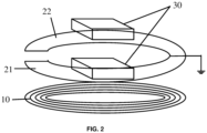
- FIGS. 1 and 2 illustrated are a layout schematic diagram and a layered schematic diagram of a printed circuit board of an electric field shielding apparatus that does not affect the transmission efficiency of a wirelessly coupled transmission coil according to an embodiment of the present invention.
- a transmission coil 10 is located at the lowest first layer, a left semi-annular metal sheet 21 and a right semi-annular metal sheet 22 are located at the third layer above the transmission coil 10, and other electronic components 30 are located at the fourth layer above the left semi-annular metal sheet 21 and the right semi-annular metal sheet 22.
- the left semi-annular metal sheet 21 and the right semi-annular metal sheet 22 have an outer ring diameter greater than or equal to the maximum diameter of the transmission coil 10, and an inner ring diameter less than or equal to the minimum diameter of the transmission coil 10.
- the top of the circular ring composed of the left semi-annular metal sheet 21 and the right semi-annular metal sheet 22 is provided with a gap greater than one tenth of the maximum coil diameter, and the bottoms of the semi-annular metal sheets are connected to each other and are grounded where they are connected.
- the left semi-annular metal sheet 21, the right semi-annular metal sheet 22 and the transmission coil 10 are on the same printed circuit board.
- the copper thickness of the left semi-annular metal sheet 21 and the right semi-annular metal sheet 22 is 35-100 microns.
- the transmission coil 10 has a maximum diameter of 10-100 mm, and a wireless coupling signal frequency of 50K-50M Hz.
- FIG. 3 is a block diagram of a wirelessly coupled transmission circuit of a specific application example in an electric field shielding apparatus that does not affect the transmission efficiency of a wirelessly coupled transmission coil according to an embodiment of the present invention.
- Table 1 is a comparison table of test results obtained by adding no electric field shielding apparatus, a fully-enclosed electric field shielding apparatus, and an electric field shielding apparatus with a gap. It can be determined from table 1 that when the traditional fully enclosed electric field shielding apparatus is used, the inductance value of the transmission coil is reduced by 44.2%, and the transmission efficiency is reduced by 29.8%; and when the electric field shielding apparatus in the embodiment of the present invention is used, the inductance value is reduced by 0.964%, and the transmission efficiency is reduced by 3%. Hence, the electric field shielding apparatus in the embodiment of the present invention has much less effect on the transmission efficiency of the wirelessly coupled transmission coil than the traditional electric field shielding apparatus.
- Table 1 is a comparison table of test results of adding no electric field shielding apparatus, adding a fully-enclosed electric field shielding apparatus, and adding an electric field shielding apparatus with a gap.
- Shielding condition Inductance value of transmission coil (uH) Inductance variation rate Transmission efficiency Transmission efficiency variation rate No shielding 3.008 - 53.3% - Fully enclosed electric field shielding apparatus 1.678 -44.2% 37.4% -29.8% Electric field shielding apparatus with a gap 2.979 -0.964% 51.7% -3.0%
- FIG. 4 is a comparison diagram of electromagnetic radiation of a specific application example in an electric field shielding apparatus that does not affect the transmission efficiency of a wirelessly coupled transmission coil according to an embodiment of the present invention.
- the abscissa represents the frequency (in Hz)
- the ordinate represents the electromagnetic radiation intensity (in dBuV/m).
- the transmission coil uses no shielding apparatus
- the transmission coil uses the shielding apparatus in the embodiment of the present invention.
- the electromagnetic radiation intensity in FIG. (b) is much less than that in FIG. (a), which proves that the shielding apparatus in the embodiment of the present invention has an obvious shielding effect on electromagnetic radiation.
- the circuit of the present invention can effectively reduce electric field radiation of wirelessly coupled transmission, has a little effect on the transmission efficiency of a transmission coil, and is easy to implement; and other circuit components are placed above the apparatus, thereby effectively reducing the circuit area of the transmission coil.
Landscapes
- Engineering & Computer Science (AREA)
- Power Engineering (AREA)
- Computer Networks & Wireless Communication (AREA)
- Physics & Mathematics (AREA)
- Electromagnetism (AREA)
- Shielding Devices Or Components To Electric Or Magnetic Fields (AREA)
Description
- The present invention relates to the field of implantable medical devices, and in particular, to an electric field shielding apparatus that does not affect the transmission efficiency of a wirelessly coupled transmission coil.
-
US 2017/084991 A1 describes an antenna structure for wireless power transfer including a ground plane configured to prevent passage of an electric field. At least one coil is configured as an antenna and located over the ground plane. The ground plane is contiguous over the coil. An insulator is located between the ground plane and the at least one coil. A shield is adjacent the coil, the shield comprising a non-contiguous structure, and is configured to allow the passage of a magnetic field to the at least one coil. -
US 2015/122884 A1 describes a non-contact communication module having a substrate including an antenna including an antenna coil placed annularly in the substrate, and a ground pattern for grounding formed in the substrate. An antenna-side land is formed on an external surface of the substrate, and is electrically connected to the antenna. A ground-side land is formed on the external surface of the substrate, and is electrically connected to the ground pattern. A distance between the antenna-side land and the ground-side land is such that the antenna-side land and the ground-side land can be connected by use of a solder bridge. - In implantable medical devices, the way of transmitting data and energy in a wirelessly coupled manner is widely applied; however, in actual application processes, the near field strong coupling manner is prone to produce multiple harmonics and electric field radiation, causing electromagnetic radiation indices to exceed the standard. To solve this problem, we usually choose to use shielding measures. The usual shielding measures generally use a well-grounded metal mesh or cover to achieve electromagnetic shielding; however, this method causes a time-varying magnetic field in a transmission coil to induce a voltage when it is close to the shielding metal, thereby generating an eddy current on the metal plane. According to Lenz's law, the eddy current will produce a magnetic flux that resists excitation, resulting in an equivalent reduction in the number of magnetic turns of the transmission coil, thus causing a weakening of the transmission magnetic field, and a serious decrease in the inductance value of the transmission coil, thereby affecting circuit resonance, reducing wirelessly coupled transmission efficiency, and increasing the power consumption of this type of circuit.
- In view of this, the object of the present invention is to provide an electric field shielding apparatus that does not affect the transmission efficiency of a wirelessly coupled transmission coil, the shielding apparatus can be used to effectively reduce the electric field radiation of a wirelessly coupled transmission circuit, the shielding apparatus has little effect on wireless transmission efficiency and wirelessly coupled resonance, and other circuit components are placed above the shielding apparatus, so that the circuit area of the transmission coil can be effectively reduced, and the entire apparatus has advantages such as simple design and easy implementation.
- In order to achieve the described object, the present invention provides an electronic circuit as defined by the appended claims.
- The beneficial effects of the present invention lie in that: the apparatus has little effect on the transmission efficiency of a transmission coil, is easy to implement, and can effectively reduce the electric field radiation of wirelessly coupled transmission; and other circuit components are placed above the apparatus, thereby effectively reducing the circuit area of the transmission coil.
- To make the object, technical solutions, and beneficial effects of the present invention clearer, the present invention provides the following description with reference to the accompanying drawings:
-
FIG. 1 is a layout schematic diagram of a printed circuit board of a specific application example in an electric field shielding apparatus that does not affect the transmission efficiency of a wirelessly coupled transmission coil according to an embodiment of the present invention; -
FIG. 2 is a layered schematic diagram of a printed circuit board of a specific application example in an electric field shielding apparatus that does not affect the transmission efficiency of a wirelessly coupled transmission coil according to an embodiment of the present invention; -
FIG. 3 is a block diagram of a wirelessly coupled transmission circuit of a specific application example in an electric field shielding apparatus that does not affect the transmission efficiency of a wirelessly coupled transmission coil according to an embodiment of the present invention; -
FIG. 4 is a comparison diagram of electromagnetic radiation of a specific application example in the electric field shielding apparatus that does not affect the transmission efficiency of a wirelessly coupled transmission coil according to the embodiment of the present invention. - Hereinafter, preferred embodiments of the present invention will be described in detail with reference to the accompanying drawings.
- Referring to
FIGS. 1 and2 , illustrated are a layout schematic diagram and a layered schematic diagram of a printed circuit board of an electric field shielding apparatus that does not affect the transmission efficiency of a wirelessly coupled transmission coil according to an embodiment of the present invention. - Taking a four-layer printed circuit board as an example, a
transmission coil 10 is located at the lowest first layer, a leftsemi-annular metal sheet 21 and a rightsemi-annular metal sheet 22 are located at the third layer above thetransmission coil 10, and otherelectronic components 30 are located at the fourth layer above the leftsemi-annular metal sheet 21 and the rightsemi-annular metal sheet 22. - In a specific embodiment, the left
semi-annular metal sheet 21 and the rightsemi-annular metal sheet 22 have an outer ring diameter greater than or equal to the maximum diameter of thetransmission coil 10, and an inner ring diameter less than or equal to the minimum diameter of thetransmission coil 10. - The top of the circular ring composed of the left
semi-annular metal sheet 21 and the rightsemi-annular metal sheet 22 is provided with a gap greater than one tenth of the maximum coil diameter, and the bottoms of the semi-annular metal sheets are connected to each other and are grounded where they are connected. - Other
electronic components 30 and wirings are provided above the leftsemi-annular metal sheet 21 and the rightsemi-annular metal sheet 22, and do not interfere with the transmission coil. - The left
semi-annular metal sheet 21, the rightsemi-annular metal sheet 22 and thetransmission coil 10 are on the same printed circuit board. - The copper thickness of the left
semi-annular metal sheet 21 and the rightsemi-annular metal sheet 22 is 35-100 microns. - The
transmission coil 10 has a maximum diameter of 10-100 mm, and a wireless coupling signal frequency of 50K-50M Hz. -
FIG. 3 is a block diagram of a wirelessly coupled transmission circuit of a specific application example in an electric field shielding apparatus that does not affect the transmission efficiency of a wirelessly coupled transmission coil according to an embodiment of the present invention. After an input signal is amplified by apower amplifier 1, the signal is transmitted to a receivingcoil 40 by means of atransmission coil 10 in a wirelessly coupled manner, and the receivingcoil 40 transmits the received signal and energy to a lower-level circuit of the implant by means of arectifier circuit 50. By adding the leftsemi-annular metal sheet 21 and the rightsemi-annular metal sheet 22 of the present invention above thetransmission coil 10, the loop of an eddy current is cut off, and the effect of the eddy current on the wirelessly coupled efficiency is avoided. Table 1 is a comparison table of test results obtained by adding no electric field shielding apparatus, a fully-enclosed electric field shielding apparatus, and an electric field shielding apparatus with a gap. It can be determined from table 1 that when the traditional fully enclosed electric field shielding apparatus is used, the inductance value of the transmission coil is reduced by 44.2%, and the transmission efficiency is reduced by 29.8%; and when the electric field shielding apparatus in the embodiment of the present invention is used, the inductance value is reduced by 0.964%, and the transmission efficiency is reduced by 3%. Hence, the electric field shielding apparatus in the embodiment of the present invention has much less effect on the transmission efficiency of the wirelessly coupled transmission coil than the traditional electric field shielding apparatus.Table 1 is a comparison table of test results of adding no electric field shielding apparatus, adding a fully-enclosed electric field shielding apparatus, and adding an electric field shielding apparatus with a gap. Shielding condition Inductance value of transmission coil (uH) Inductance variation rate Transmission efficiency Transmission efficiency variation rate No shielding 3.008 - 53.3% - Fully enclosed electric field shielding apparatus 1.678 -44.2% 37.4% -29.8% Electric field shielding apparatus with a gap 2.979 -0.964% 51.7% -3.0% -
FIG. 4 is a comparison diagram of electromagnetic radiation of a specific application example in an electric field shielding apparatus that does not affect the transmission efficiency of a wirelessly coupled transmission coil according to an embodiment of the present invention. In FIGS. (a) and (b), the abscissa represents the frequency (in Hz), and the ordinate represents the electromagnetic radiation intensity (in dBuV/m). In FIG. (a), the transmission coil uses no shielding apparatus, and in FIG. (b), the transmission coil uses the shielding apparatus in the embodiment of the present invention. The electromagnetic radiation intensity in FIG. (b) is much less than that in FIG. (a), which proves that the shielding apparatus in the embodiment of the present invention has an obvious shielding effect on electromagnetic radiation. - The circuit of the present invention can effectively reduce electric field radiation of wirelessly coupled transmission, has a little effect on the transmission efficiency of a transmission coil, and is easy to implement; and other circuit components are placed above the apparatus, thereby effectively reducing the circuit area of the transmission coil.
- Finally, it should be noted that the preferred embodiments above are only intended to illustrate the technical solutions of the present invention, but not to limit the present invention. Although the present invention has been described in detail through the preferred embodiments above, a person skilled in the art should understand that various changes can be made in form and detail without departing from the scope of the present invention as defined in the claims.
Claims (6)
- A electronic circuit having a transmission coil (10), an electric field shielding apparatus, and other electronic components (30), wherein said electric field shielding apparatus does not affect the transmission efficiency of said wirelessly coupled transmission coil (10), wherein the electric field shielding apparatus is composed of two semi-annular metal sheets (21, 22), wherein both semi-annular metal sheets are provided above said transmission coil,wherein bottoms of the semi-annular metal sheets are connected,wherein a top of the circular ring composed of the two semi-annular metal sheets is provided with a gap,wherein the bottoms of the semi-annular metal sheets are grounded where they are connected,characterized in thatsaid electronic circuit has wirings which are placed with the electronic components above the semi-annular metal sheets,wherein said electronic components and wirings do not interfere with the transmission coil, wherein said gap is greater than one tenth of the diameter of the maximum diameter of said transmission coil.
- The electronic circuit according to claim 1, characterized in that the semi-annular metal sheets have an outer ring diameter greater than or equal to the maximum diameter of the transmission coil, and an inner ring diameter less than or equal to the minimum diameter of the transmission coil.
- The electronic circuit according to claim 1, characterized in that the semi-annular metal sheets and the transmission coil are on a same printed circuit board.
- The electronic circuit according to claim 1, characterized in that the copper thickness of the semi-annular metal sheets is 35-100 microns.
- The electronic circuit according to claim 1, characterized in that the maximum diameter of the transmission coil is 10-100 mm.
- The electronic circuit according to claim 1, characterized in that the transmission coil has a wireless coupling signal frequency of 50 kHz to 50 MHz.
Applications Claiming Priority (2)
| Application Number | Priority Date | Filing Date | Title |
|---|---|---|---|
| CN201910562397.6A CN110289046A (en) | 2019-06-26 | 2019-06-26 | A kind of electric field shielding device not influencing wireless coupling transmission coil efficiency of transmission |
| PCT/CN2019/096645 WO2020258411A1 (en) | 2019-06-26 | 2019-07-19 | Electric field shielding apparatus that does not affect transmission efficiency of wirelessly coupled transmission coil |
Publications (3)
| Publication Number | Publication Date |
|---|---|
| EP3975188A1 EP3975188A1 (en) | 2022-03-30 |
| EP3975188A4 EP3975188A4 (en) | 2022-08-03 |
| EP3975188B1 true EP3975188B1 (en) | 2024-02-14 |
Family
ID=68006287
Family Applications (1)
| Application Number | Title | Priority Date | Filing Date |
|---|---|---|---|
| EP19935741.9A Active EP3975188B1 (en) | 2019-06-26 | 2019-07-19 | Electric field shielding apparatus that does not affect transmission efficiency of wirelessly coupled transmission coil |
Country Status (3)
| Country | Link |
|---|---|
| EP (1) | EP3975188B1 (en) |
| CN (1) | CN110289046A (en) |
| WO (1) | WO2020258411A1 (en) |
Family Cites Families (13)
| Publication number | Priority date | Publication date | Assignee | Title |
|---|---|---|---|---|
| JPS60140287A (en) * | 1983-12-28 | 1985-07-25 | Mita Ind Co Ltd | Destaticizing lamp device |
| US20030139662A1 (en) * | 2001-10-16 | 2003-07-24 | Seidman Abraham Neil | Method and apparatus for detecting, identifying and performing operations on microstructures including, anthrax spores, brain cells, cancer cells, living tissue cells, and macro-objects including stereotactic neurosurgery instruments, weapons and explosives |
| US8350655B2 (en) * | 2003-02-26 | 2013-01-08 | Analogic Corporation | Shielded power coupling device |
| US8060218B2 (en) * | 2007-08-02 | 2011-11-15 | Synecor, Llc | Inductive element for intravascular implantable devices |
| JP2015008547A (en) * | 2011-10-28 | 2015-01-15 | パナソニック株式会社 | Non-contact power charger |
| JP6145388B2 (en) * | 2013-10-30 | 2017-06-14 | 日本電産サンキョー株式会社 | Contactless communication module and card reader |
| CN105101767B (en) * | 2015-07-02 | 2019-04-09 | 宁波微鹅电子科技有限公司 | Electromagnetic armouring structure and power transfer with electromagnetic armouring structure |
| CN105050372B (en) * | 2015-09-09 | 2019-05-17 | 宁波微鹅电子科技有限公司 | A kind of electro-magnetic screen layer and the wireless electric energy transmission device with electro-magnetic screen layer |
| US20170084991A1 (en) * | 2015-09-17 | 2017-03-23 | Qualcomm Incorporated | Wireless power transfer antenna having a split shield |
| JP6822761B2 (en) * | 2015-10-30 | 2021-01-27 | キヤノンメディカルシステムズ株式会社 | Medical diagnostic imaging system, magnetic resonance imaging device and video projection program |
| CN105871074B (en) * | 2015-12-20 | 2020-04-28 | 华南理工大学 | Wireless energy transmission coil system for counteracting and inhibiting frequency splitting through magnetoelectric coupling |
| CN207352061U (en) * | 2017-11-14 | 2018-05-11 | 海南电网有限责任公司电力科学研究院 | A kind of Rogowski coil for being used to measure weak current traveling wave |
| CN209928986U (en) * | 2019-06-26 | 2020-01-10 | 浙江诺尔康神经电子科技股份有限公司 | Electric field shielding device without influencing transmission efficiency of wireless coupling transmission coil |
-
2019
- 2019-06-26 CN CN201910562397.6A patent/CN110289046A/en active Pending
- 2019-07-19 WO PCT/CN2019/096645 patent/WO2020258411A1/en unknown
- 2019-07-19 EP EP19935741.9A patent/EP3975188B1/en active Active
Also Published As
| Publication number | Publication date |
|---|---|
| EP3975188A1 (en) | 2022-03-30 |
| CN110289046A (en) | 2019-09-27 |
| EP3975188A4 (en) | 2022-08-03 |
| WO2020258411A1 (en) | 2020-12-30 |
Similar Documents
| Publication | Publication Date | Title |
|---|---|---|
| TWI402866B (en) | Suspension inductor devices | |
| EP2546843B1 (en) | Magnetic element for wireless power transmission and power supply device | |
| KR101539879B1 (en) | Chip electronic component | |
| US20120071088A1 (en) | NFC Card for Handheld Device | |
| KR20070004426A (en) | Circuit board, electronic apparatus, and power supply | |
| US20110006872A1 (en) | Magnetic shield layout, semiconductor device and application | |
| KR101807604B1 (en) | Antenna unit for wireless power transfer and Wireless power transmission module having the same | |
| US20190098805A1 (en) | Magnetic shielding tape for cable and method for manufacturing thereof | |
| US20190252781A1 (en) | Coil device | |
| JP6669250B2 (en) | Power receiving device | |
| CN107801296A (en) | The printed circuit board (PCB) and terminal device of fringe radiation can be reduced | |
| EP3975188B1 (en) | Electric field shielding apparatus that does not affect transmission efficiency of wirelessly coupled transmission coil | |
| WO2011140031A1 (en) | Magnetically shielded inductor structure | |
| JP5659504B2 (en) | Electromagnetic wave characteristic improvement sheet | |
| CN209928986U (en) | Electric field shielding device without influencing transmission efficiency of wireless coupling transmission coil | |
| JP2006178713A (en) | Information processor | |
| JP2017017175A (en) | Multilayer wiring board, high-frequency circuit, communication device, and method of manufacturing multilayer wiring board | |
| JP2012238797A (en) | Multilayer circuit module | |
| KR20160126350A (en) | Transformer and power supply apparatus including the same | |
| US20210259092A1 (en) | Multi-Stack Cooling Structure for Radiofrequency Component | |
| JP2010010550A (en) | Mounting structure of electronic part | |
| KR101616787B1 (en) | Magnetic shielding sheet and method for manufacturing the same | |
| KR101642612B1 (en) | Inductor and Method of Fabricating the Same | |
| CN110781696B (en) | Non-contact communication module and card reader | |
| KR101603562B1 (en) | Magnetic shielding sheet |
Legal Events
| Date | Code | Title | Description |
|---|---|---|---|
| STAA | Information on the status of an ep patent application or granted ep patent |
Free format text: STATUS: THE INTERNATIONAL PUBLICATION HAS BEEN MADE |
|
| PUAI | Public reference made under article 153(3) epc to a published international application that has entered the european phase |
Free format text: ORIGINAL CODE: 0009012 |
|
| STAA | Information on the status of an ep patent application or granted ep patent |
Free format text: STATUS: REQUEST FOR EXAMINATION WAS MADE |
|
| 17P | Request for examination filed |
Effective date: 20211221 |
|
| AK | Designated contracting states |
Kind code of ref document: A1 Designated state(s): AL AT BE BG CH CY CZ DE DK EE ES FI FR GB GR HR HU IE IS IT LI LT LU LV MC MK MT NL NO PL PT RO RS SE SI SK SM TR |
|
| REG | Reference to a national code |
Ref document number: 602019046749 Country of ref document: DE Ref country code: DE Ref legal event code: R079 Free format text: PREVIOUS MAIN CLASS: G12B0017020000 Ipc: H01F0027360000 |
|
| A4 | Supplementary search report drawn up and despatched |
Effective date: 20220701 |
|
| RIC1 | Information provided on ipc code assigned before grant |
Ipc: H01F 38/14 20060101ALN20220627BHEP Ipc: H02J 50/10 20160101ALI20220627BHEP Ipc: G12B 17/02 20060101ALI20220627BHEP Ipc: H01F 5/00 20060101ALI20220627BHEP Ipc: H01F 27/36 20060101AFI20220627BHEP |
|
| DAV | Request for validation of the european patent (deleted) | ||
| DAX | Request for extension of the european patent (deleted) | ||
| STAA | Information on the status of an ep patent application or granted ep patent |
Free format text: STATUS: EXAMINATION IS IN PROGRESS |
|
| 17Q | First examination report despatched |
Effective date: 20230322 |
|
| GRAP | Despatch of communication of intention to grant a patent |
Free format text: ORIGINAL CODE: EPIDOSNIGR1 |
|
| STAA | Information on the status of an ep patent application or granted ep patent |
Free format text: STATUS: GRANT OF PATENT IS INTENDED |
|
| RIC1 | Information provided on ipc code assigned before grant |
Ipc: H01F 38/14 20060101ALN20230911BHEP Ipc: H02J 50/10 20160101ALI20230911BHEP Ipc: G12B 17/02 20060101ALI20230911BHEP Ipc: H01F 5/00 20060101ALI20230911BHEP Ipc: H01F 27/36 20060101AFI20230911BHEP |
|
| INTG | Intention to grant announced |
Effective date: 20231012 |
|
| GRAS | Grant fee paid |
Free format text: ORIGINAL CODE: EPIDOSNIGR3 |
|
| GRAA | (expected) grant |
Free format text: ORIGINAL CODE: 0009210 |
|
| STAA | Information on the status of an ep patent application or granted ep patent |
Free format text: STATUS: THE PATENT HAS BEEN GRANTED |
|
| AK | Designated contracting states |
Kind code of ref document: B1 Designated state(s): AL AT BE BG CH CY CZ DE DK EE ES FI FR GB GR HR HU IE IS IT LI LT LU LV MC MK MT NL NO PL PT RO RS SE SI SK SM TR |
|
| REG | Reference to a national code |
Ref country code: GB Ref legal event code: FG4D |
|
| REG | Reference to a national code |
Ref country code: CH Ref legal event code: EP |
|
| REG | Reference to a national code |
Ref country code: DE Ref legal event code: R096 Ref document number: 602019046749 Country of ref document: DE |
|
| REG | Reference to a national code |
Ref country code: IE Ref legal event code: FG4D |
|
| U01 | Request for unitary effect filed |
Effective date: 20240222 |
|
| U07 | Unitary effect registered |
Designated state(s): AT BE BG DE DK EE FI FR IT LT LU LV MT NL PT SE SI Effective date: 20240301 |