EP3973383B1 - Solutions à voies multiples pour adresser des éléments vectoriels à l'aide de registres d'indices vectoriels - Google Patents
Solutions à voies multiples pour adresser des éléments vectoriels à l'aide de registres d'indices vectoriels Download PDFInfo
- Publication number
- EP3973383B1 EP3973383B1 EP20808720.5A EP20808720A EP3973383B1 EP 3973383 B1 EP3973383 B1 EP 3973383B1 EP 20808720 A EP20808720 A EP 20808720A EP 3973383 B1 EP3973383 B1 EP 3973383B1
- Authority
- EP
- European Patent Office
- Prior art keywords
- vector
- lane
- operand
- register
- loaded
- Prior art date
- Legal status (The legal status is an assumption and is not a legal conclusion. Google has not performed a legal analysis and makes no representation as to the accuracy of the status listed.)
- Active
Links
Images


Classifications
-
- G—PHYSICS
- G06—COMPUTING OR CALCULATING; COUNTING
- G06F—ELECTRIC DIGITAL DATA PROCESSING
- G06F9/00—Arrangements for program control, e.g. control units
- G06F9/06—Arrangements for program control, e.g. control units using stored programs, i.e. using an internal store of processing equipment to receive or retain programs
- G06F9/30—Arrangements for executing machine instructions, e.g. instruction decode
- G06F9/30003—Arrangements for executing specific machine instructions
- G06F9/30007—Arrangements for executing specific machine instructions to perform operations on data operands
- G06F9/30021—Compare instructions, e.g. Greater-Than, Equal-To, MINMAX
-
- G—PHYSICS
- G06—COMPUTING OR CALCULATING; COUNTING
- G06F—ELECTRIC DIGITAL DATA PROCESSING
- G06F9/00—Arrangements for program control, e.g. control units
- G06F9/06—Arrangements for program control, e.g. control units using stored programs, i.e. using an internal store of processing equipment to receive or retain programs
- G06F9/30—Arrangements for executing machine instructions, e.g. instruction decode
- G06F9/30098—Register arrangements
- G06F9/3012—Organisation of register space, e.g. banked or distributed register file
- G06F9/3013—Organisation of register space, e.g. banked or distributed register file according to data content, e.g. floating-point registers, address registers
-
- G—PHYSICS
- G06—COMPUTING OR CALCULATING; COUNTING
- G06F—ELECTRIC DIGITAL DATA PROCESSING
- G06F11/00—Error detection; Error correction; Monitoring
- G06F11/22—Detection or location of defective computer hardware by testing during standby operation or during idle time, e.g. start-up testing
- G06F11/26—Functional testing
-
- G—PHYSICS
- G06—COMPUTING OR CALCULATING; COUNTING
- G06F—ELECTRIC DIGITAL DATA PROCESSING
- G06F11/00—Error detection; Error correction; Monitoring
- G06F11/22—Detection or location of defective computer hardware by testing during standby operation or during idle time, e.g. start-up testing
- G06F11/2205—Detection or location of defective computer hardware by testing during standby operation or during idle time, e.g. start-up testing using arrangements specific to the hardware being tested
- G06F11/2236—Detection or location of defective computer hardware by testing during standby operation or during idle time, e.g. start-up testing using arrangements specific to the hardware being tested to test CPU or processors
-
- G—PHYSICS
- G06—COMPUTING OR CALCULATING; COUNTING
- G06F—ELECTRIC DIGITAL DATA PROCESSING
- G06F15/00—Digital computers in general; Data processing equipment in general
- G06F15/76—Architectures of general purpose stored program computers
- G06F15/80—Architectures of general purpose stored program computers comprising an array of processing units with common control, e.g. single instruction multiple data processors
- G06F15/8053—Vector processors
-
- G—PHYSICS
- G06—COMPUTING OR CALCULATING; COUNTING
- G06F—ELECTRIC DIGITAL DATA PROCESSING
- G06F9/00—Arrangements for program control, e.g. control units
- G06F9/06—Arrangements for program control, e.g. control units using stored programs, i.e. using an internal store of processing equipment to receive or retain programs
- G06F9/30—Arrangements for executing machine instructions, e.g. instruction decode
- G06F9/30003—Arrangements for executing specific machine instructions
- G06F9/30007—Arrangements for executing specific machine instructions to perform operations on data operands
- G06F9/3001—Arithmetic instructions
-
- G—PHYSICS
- G06—COMPUTING OR CALCULATING; COUNTING
- G06F—ELECTRIC DIGITAL DATA PROCESSING
- G06F9/00—Arrangements for program control, e.g. control units
- G06F9/06—Arrangements for program control, e.g. control units using stored programs, i.e. using an internal store of processing equipment to receive or retain programs
- G06F9/30—Arrangements for executing machine instructions, e.g. instruction decode
- G06F9/30003—Arrangements for executing specific machine instructions
- G06F9/30007—Arrangements for executing specific machine instructions to perform operations on data operands
- G06F9/30036—Instructions to perform operations on packed data, e.g. vector, tile or matrix operations
-
- G—PHYSICS
- G06—COMPUTING OR CALCULATING; COUNTING
- G06F—ELECTRIC DIGITAL DATA PROCESSING
- G06F9/00—Arrangements for program control, e.g. control units
- G06F9/06—Arrangements for program control, e.g. control units using stored programs, i.e. using an internal store of processing equipment to receive or retain programs
- G06F9/30—Arrangements for executing machine instructions, e.g. instruction decode
- G06F9/30098—Register arrangements
- G06F9/30101—Special purpose registers
-
- G—PHYSICS
- G06—COMPUTING OR CALCULATING; COUNTING
- G06F—ELECTRIC DIGITAL DATA PROCESSING
- G06F9/00—Arrangements for program control, e.g. control units
- G06F9/06—Arrangements for program control, e.g. control units using stored programs, i.e. using an internal store of processing equipment to receive or retain programs
- G06F9/30—Arrangements for executing machine instructions, e.g. instruction decode
- G06F9/34—Addressing or accessing the instruction operand or the result ; Formation of operand address; Addressing modes
- G06F9/355—Indexed addressing
- G06F9/3555—Indexed addressing using scaling, e.g. multiplication of index
-
- G—PHYSICS
- G06—COMPUTING OR CALCULATING; COUNTING
- G06F—ELECTRIC DIGITAL DATA PROCESSING
- G06F9/00—Arrangements for program control, e.g. control units
- G06F9/06—Arrangements for program control, e.g. control units using stored programs, i.e. using an internal store of processing equipment to receive or retain programs
- G06F9/30—Arrangements for executing machine instructions, e.g. instruction decode
- G06F9/38—Concurrent instruction execution, e.g. pipeline or look ahead
- G06F9/3867—Concurrent instruction execution, e.g. pipeline or look ahead using instruction pipelines
Definitions
- At least some embodiments disclosed herein relate to vector processors using multi-lane solutions. Also, at least some embodiments disclosed herein relate to registers in vector processors that use multi-lane solutions for storing addresses for accessing vectors.
- a vector processor can be or include a central processing unit (CPU) that implements an instruction set containing instructions that operate on arrays of data of commonly referred to as vectors. This is different from a scalar processor, wherein instructions operate on single data items.
- Vector processors can greatly improve performance on certain workloads over scalar processor, notably numerical simulation and similar tasks.
- Vector processors appeared in the early 1970s and where a large part of supercomputing design through the 1970s into the 1990s. The rapid fall in the price-to-performance ratio of more conventional microprocessor designs, such as scalar processor designs, as led to less development and manufacturing of vector processors.
- conventional CPUs e.g., scalar based CPUs
- scalar based CPUs are able to manipulate a few pieces of data at a time, at most.
- such CPUs have an instruction that essentially provide adding A to B and store the result in C.
- the data for A, B and C is usually pointed to by passing in an address to a memory location that holds the data. Decoding this address and getting the data out of the memory takes some time, during which the CPU can sit idle waiting for the requested data to show up.
- Vector processors improve on pipelining by, instead of pipelining merely the instructions, such processors also pipeline the data itself. Thus, instead of constantly having to decode instructions and then fetch the data needed to complete the instructions, the vector processor reads a single instruction from memory. This allows for reduced decoding time and reduced power consumption (e.g., one decode with vector processors instead of multiple decodes).
- Vector processors as well as other types of processors, such as the commonly used scalar processors, include index registers for modifying operand addresses during the execution of a program or operation. Often indexes are used and beneficial for doing vector or array operations. The contents of an index register can be added to or subtracted from an immediate address to form an effective address of the actual data or operand. Commonly, instructions can test the index register and, if the test fails, the instructions can reset the start of the loop. In this situation an index register is used for loop control. Some instruction sets allow multiple index registers to be used.
- scalar registers for indexing.
- a scalar register for indexing.
- some of these limitations can curb the performance of a processor using the index register. For example, to access multiple positions of an operand vector, a scalar index register needs to be incremented and each incrementation needs to be separately loaded by the processor to be used for accessing the operand vector.
- US6269435 discloses a system which loads vector data from memory and tests it upon a certain condition. The results are stored into different registers.
- At least some embodiments disclosed herein relate to vector processors using multi-lane solutions. Also, at least some of the embodiments disclosed herein include vector index registers in vector processors that each store multiple addresses for accessing multiple positions in operand vectors. And, in at least some of the embodiments disclosed herein, multi-lane solutions can enhance the storing of addresses by vector index registers and the accessing of multiple positions in operand vectors.
- At least some of the embodiments disclosed herein include vector index registers for TRUE and/or FALSE results of one or more conditional test operations (such as numerical comparisons) that each store multiple addresses for accessing multiple positions in operand vectors (VIR_TRUE and VIR_FALSE). Also, at least some embodiments described herein are directed to conditional operations in a vector processor having vector index registers VIR_TRUE and VIR_FALSE. Further, disclosed herein are processes of using VIR_TRUE and VIR_FALSE, including multi-lane processes, for more efficiently executing conditional operations in a vector processor.
- a scalar index register in a vector processor to reference multiple positions of vectors by changing the value stored in the scalar index register during a vector operation.
- the scalar index register can be replaced and at least the continual changing of values in the scalar index register during a vector operation can be avoided. This is just one example of a technical solution to a technical problem described herein.
- there are other limitations associated with using a scalar register or single-entry vector for indexing can curb the performance of a vector processor using the index register.
- a scalar or single-entry index register needs to be incremented and each incrementation needs to be separately loaded by the vector processor to be used for accessing the operand vector.
- the scalar index register can be replaced and at least the continual changing of the scalar index register during a vector operation can be avoided.
- the performance of a vector processor can be enhanced even further by using vector indexing registers in combination with multi-lane solutions for storing addresses for accessing operand vectors. Also, the performance of a vector processor can be enhanced by using vector indexing registers in combination with multi-lane solutions for accessing operand vectors. This is especially the case when the vector processor performs conditional operations.
- the multiplication "X" can be replaced with another operation (e.g., addition, subtraction, bit-wise OR, etc.).
- the result of the operation on two or more vectors can be a scalar or a vector.
- a vector index register can store address components for vector operations that use selective indexing. For example, using selective indexing, a VIR can store address parts i_1, i_2, ..., i_n. This allows the operations on a vector register to move through elements i_1, i_2, ..., i_n of an input vector, instead of i, i+1, i+2, ... i+n of the input vector. For example, using selective indexing, a VIR can store non-sequential address parts i_1, i_3, ..., i_8. This allows the operations on a vector register to move through non-sequential elements of an input vector.
- multiple lanes can enhance selective indexing.
- the time expended for selective indexing can at least be cut in half by dividing the selective indexing into at least two lanes.
- a VIR can store address parts i_1, i_2, ..., i_n at least two at a time.
- every other address part can be stored in an even position of the VIR, and the other address parts can be stored in odd positions of the VIR in parallel.
- multiple lanes allows the operations on a vector register to move through elements i_1, i_2, ..., i_n of an input vector at least twice as fast as well.
- the accessing of elements i_1, i_2, ..., i_n instead of i, i+1, i+2, ... i+n of the input vector can also occur by accessing every other address part stored in even positions and the other parts stored in odd positions in parallel, for instance.
- a VIR can store non-sequential address parts i_1, i_3, ..., i_8 and the processor can access such parts more quickly by splitting the processing into multiple lanes.
- the technologies disclosed herein can at least provide support for basic or complex conditional operations.
- VIR_TRUE A(VIR_TRUE(j)) + B(VIR_TRUE(j))
- A(VIR_FALSE(k)) A(VIR_FALSE(k)) - B(VIR_FALSE(k)).
- the results of the test conditions can also be used to set the indices in the two vector index registers, VIR_TRUE and VIR_FALSE.
- the technologies disclosed herein can also enhance basic or complex conditional operations with the use of multiple lanes or multiple lane vector processing.
- the technologies utilize a multi-lane solution for conditional operations in a vector processor having vector index registers VIR_TRUE and VIR_FALSE.
- the multi-lane solutions can more efficiently or quickly process vector conditional operations in a vector processor.
- This disclosure provides basic conditional operations as examples for showing the use of VIRs with multiple lane vector processing, but it is to be understood that the techniques disclosed herein can be used for more complex conditional operations.
- illustrated herein are two-lane vector processing solutions; however, it is to be understood that the techniques disclosed herein can also be applied to solutions with more than two lanes, such as four lane vector processing.
- the example can be processed using two sets of TRUE and FALSE VIRs or one set of TRUE and FALSE VIRs that are dual access VIRs.
- some embodiments can include four VIRs: VIR_TRUE_Lane_0 and VIR_FALSE_Lane 0, and VIR TRUE_Lane_1 and VIR_FALSE_Lane_1.
- some embodiments can include VIR_TRUE split into two lanes, and VIR_FALSE split into two lanes.
- test condition can be simple (e.g., "A(i) > 0", or "A(i) > B(i)", or “A(i) > C(i)”) or be more complex (e.g., "(A(i) > 0 and A(i) > B(i)) or (A(i) > C(i))").
- test condition in general does not have to be testing ">".
- the test condition can be other types of numerical tests and/or Boolean operations.
- the index values or addressing components stored in a VIR can be converted to memory addresses (e.g., the base address plus increments for each memory unit).
- memory addresses e.g., the base address plus increments for each memory unit.
- the techniques disclosed herein can provide a method utilizing VIRs and multi-lane vector processing.
- the lanes in the processing in the method can be implemented by even and odd positions in the operand vectors.
- even positions in each operand vector can be in a first lane and odd positions in each operand vector can be in a second lane from example.
- the operand vector registers used in the method can be dual-access operand vector registers.
- multiplexors can be used to achieve similar functionality in the method without dual-access operand vectors.
- such examples using regular operand vector registers can have more complex circuit design than examples using dual-access operand vector registers or multi-access operand vector registers.
- the method can include loading, by a vector load-store unit of a vector processor, one or more operand vectors. Each vector of the one or more operand vectors being stored in a respective operand vector register.
- the method can also include performing, by the vector processor, a conditional test operation on each element at a first lane index position of at least one of the loaded one or more operand vectors according to a first lane count stored in a first lane counter register.
- the conditional test operations can provide a vector of test results.
- the method can also include storing, in a first lane index position in a first vector index register for each TRUE result of TRUE results of the conditional test operation (VIR_TRUE), a position of the TRUE result in the vector of test results according to the first lane count.
- the method can also include storing, in a first lane index position in a second vector index register for each FALSE result of FALSE results of the conditional test operation (VIR_FALSE), a position of the FALSE result in the vector of test results according to the first lane count.
- the method can also include performing, by the vector processor, the conditional test operation on each element at a second lane index position of at least one of the loaded one or more operand vectors according to a second lane count stored in a second lane counter register. And, the method can include storing, in a second lane index position in the VIR_TRUE, a position of the TRUE result in the vector of test results according to the second lane count, as well as storing, in a second lane index position in the VIR_FALSE, a position of the FALSE result in the vector of test results according to the second lane count.
- the method can also include performing a first vector operation on first elements in the one or more operand vectors.
- the method can also include performing a second vector operation on second elements in the one or more operand vectors.
- the method can also include loading, by a vector load-store unit, a first input operand vector stored in a first input operand vector register, as well as loading, by the vector load-store unit, a second input operand vector stored in a second input operand vector register.
- the method can also include loading from the VIR_TRUE, by the vector load-store unit, a stored position of respective elements of the loaded first and second input operand vectors according to a first lane count, as well as loading from the VIR_TRUE, by the vector load-store unit, a stored position of respective elements of the loaded first and second input operand vectors according to a second lane count.
- the method can also include executing a first operation over the respective elements of the loaded first and second input operand vectors according to the loaded positions from the first lane and the second lane in the VIR_TRUE.
- the first input operand vector register can be a dual-access operand vector register
- the second input operand vector register can be a dual-access operand vector register.
- the method can also include storing the result of the first operation into an output operand vector register at positions that correspond to the loaded positions from the first and second lanes in the VIR_TRUE.
- the method can also include continuing to execute the first operation over respective elements of the loaded first and second input operand vectors according to loaded positions from the first lane and the second lane in the VIR_TRUE and to store the results of the first operation into the output operand vector register at the corresponding positions that match the loaded positions from the VIR_TRUE, until the first lane count or the second lane count exceeds or equals the length of the VIR_TRUE.
- the method can include resetting the first lane count and the second lane count when the first lane count or the second lane count exceeds or equals the length of the VIR_TRUE.
- the first lane count and the second lane count can each be incremented by two per loaded position from the VIR_TRUE.
- the method can also include, subsequent to resetting the first lane count and the second lane count, loading from the VIR_FALSE, by the vector load-store unit, a stored position of respective elements of the loaded first and second input operand vectors according to the first lane count. Also, subsequent to resetting the first lane count and the second lane count, the method can include loading from a VIR_FALSE, by the vector load-store unit, a stored position of respective elements of the loaded first and second input operand vectors according to the second lane count. The method can also include executing a second operation over the respective elements of the loaded first and second input operand vectors according to the loaded positions from the first lane and the second lane in VIR_FALSE.
- the method can also include continuing to execute the second operation over respective elements of the loaded first and second input operand vectors according to loaded positions from the first lane and the second lane in the VIR_FALSE and to store the results of the first operation into the output operand vector register at the corresponding positions that match the loaded positions from the VIR_FALSE, until the first lane count or the second lane count exceeds or equals the length of the VIR_FALSE.
- the first lane count and the second lane count can each be incremented by two per loaded position from the VIR_FALSE.
- the first and second operations can each include various types of numerical operations.
- the first operation can include addition and the second operation can include subtraction.
- the technologies disclosed herein can provide a system utilizing VIRs and multi-lane vector processing.
- the system can include a vector processor, configured to perform a conditional test operation on elements of a first loaded operand vector and a second loaded operand vector using two lanes within each of the first and second loaded operand vectors.
- the lanes in the processing by the system can be implemented by even and odd positions in the operand vectors.
- the operand vector registers used in the system can be dual-access operand vector registers.
- multiplexors can be used to achieve similar functionality in the system without dual-access operand vectors.
- such examples using regular operand vector registers can have more complex circuit design than examples using dual-access operand vector registers or multi-access operand vector registers.
- dual-access operand vector registers can be used in embodiments having two-lane processing.
- quad-access operand vector registers can be used in embodiments having four-lane processing.
- Using additional multiplexors instead of multiple-access operand vector registers for multiple-lane processing can make the circuit design less elegant.
- the system can also include a first lane counter of the vector processor, configured to store a first lane count.
- the system can also include a second lane counter of the vector processor, configured to store a second lane count. Performance of the conditional test operation by the vector processor can be according to the first lane count and the second lane count.
- the system can also include one or more operand vectors registers of the vector processor. Each operand vector register can be configured to store an operand vector.
- the system can also include a first vector index register for each TRUE result of TRUE results of the conditional test operation (VIR_TRUE). Also, system can include a second vector index register for each FALSE result of FALSE results of the conditional test operation (VIR_FALSE)
- the vector processor can be configured to load one or more operand vectors from the one or more operand vector registers. It can also be configured to perform a conditional test operation on each element at a first lane index position of at least one of the loaded one or more operand vectors according to a first lane count stored in the first lane counter as well as perform the conditional test operation on each element at a second lane index position of at least one of the loaded one or more operand vectors according to a second lane count stored in the second lane counter.
- the conditional test operations can provide a vector of test results.
- the vector processor in the system can also be configured to perform the operations of the aforesaid method.
- the vector processor is further configured to load, by a vector load-store unit of the vector processor, a first input operand vector stored in a first input operand vector register, as well as load, by the vector load-store unit, a second input operand vector stored in a second input operand vector register.
- the vector processor is further configured to load from the VIR_TRUE, by the vector load-store unit, a stored position of respective elements of the loaded first and second input operand vectors according to a first lane count, as well as load from the VIR_TRUE, by the vector load-store unit, a stored position of respective elements of the loaded first and second input operand vectors according to a second lane count.
- the vector process can also be configured to execute a first operation over the respective elements of the loaded first and second input operand vectors according to the loaded positions from the first lane and the second lane in the VIR_TRUE, as well as store the result of the first operation into an output operand vector register at positions that correspond to the loaded positions from the first and second lanes in the VIR_TRUE.
- It can also be configured to continue to execute the first operation over respective elements of the loaded first and second input operand vectors according to loaded positions from the first lane and the second lane in the VIR_TRUE and to store the results of the first operation into the output operand vector register at the corresponding positions that match the loaded positions from the VIR_TRUE, until the first lane count or the second lane count exceeds or equals the length of the VIR_TRUE. It can also be configured to reset the first lane count and the second lane count when the first lane count or the second lane count exceeds or equals the length of the VIR_TRUE. The first lane count and the second lane count can each be incremented by two per loaded position from the VIR_TRUE.
- the vector processor can also be further configured to, subsequent to resets of the first lane count and the second lane count, load from the VIR_FALSE, by the vector load-store unit, a stored position of respective elements of the loaded first and second input operand vectors according to the first lane count. It can also be configured to load from a VIR_FALSE, by the vector load-store unit, a stored position of respective elements of the loaded first and second input operand vectors according to the second lane count. It can also be configured to execute a second operation over the respective elements of the loaded first and second input operand vectors according to the loaded positions from the first lane and the second lane in VIR_FALSE.
- It can also be configured to continue to execute the second operation over respective elements of the loaded first and second input operand vectors according to loaded positions from the first lane and the second lane in the VIR_FALSE and to store the results of the first operation into the output operand vector register at the corresponding positions that match the loaded positions from the VIR_FALSE, until the first lane count or the second lane count exceeds or equals the length of the VIR_FALSE.
- the first lane count and the second lane count can each be incremented by two per loaded position from the VIR_FALSE.
- the vector processor can also be configured to perform a conditional test operation on elements of the first OVR and the second OVR according to a first lane count stored in the first lane count register and a second lane count stored in a second lane count register. Also, the vector processor can be configured to perform a conditional test operation on an element stored in the OSR and elements of the first OVR according to a first lane count stored in the first lane count register and a second lane count stored in a second lane count register.
- the conditional test operations can provide a vector of test results.
- the vector processor can also include a first vector index register (VIR_TRUE) configured to store, in a first lane index position in the VIR_TRUE, a position of a TRUE result in the vector of test results according to the first lane count, as well as store, in a second lane index position in the VIR_TRUE, a position of a TRUE result in the vector of test results according to the second lane count.
- VIR_TRUE first vector index register
- the processor can also include a second vector index register (VIR_FALSE) configured to store, in a first lane index position in the VIR_FALSE, a position of a FALSE result in the vector of test results according to the first lane count, as well as store, in a second lane index position in the VIR_FALSE, a position of a FALSE result in the vector of test results according to the second lane count.
- VIR_FALSE second vector index register
- the vector processor can be configured to perform the operations of the aforesaid method.
- FIG. 1 illustrates example parts of an example computing device 100, in accordance with some embodiments of the present disclosure.
- the device 100 can be communicatively coupled to one or more networks 112, as shown.
- the device 100 includes a vector processor 102 that is in accordance with some embodiments of the present disclosure.
- the device 100 also includes at least a bus 104, a main memory 106, a data storage system 108, and a network interface 110.
- the bus 104 communicatively couples the vector processor 102, the main memory 106, the data storage system 108, and the network interface 110.
- the device 100 includes a computer system that includes at least vector processor 102, main memory 106 (e.g., read-only memory (ROM), flash memory, dynamic random access memory (DRAM) such as synchronous DRAM (SDRAM) or Rambus DRAM (RDRAM), static random access memory (SRAM), etc.), and data storage system 108, which communicate with each other via bus 104 (which can include multiple buses).
- main memory 106 e.g., read-only memory (ROM), flash memory, dynamic random access memory (DRAM) such as synchronous DRAM (SDRAM) or Rambus DRAM (RDRAM), static random access memory (SRAM), etc.
- DRAM dynamic random access memory
- SDRAM synchronous DRAM
- RDRAM Rambus DRAM
- SRAM static random access memory
- FIG. 1 is a block diagram of an example device 100 having a computer system in which embodiments of the present disclosure can operate.
- the computer system can include a set of instructions, for causing a machine to perform any one or more of the methodologies discussed herein, when executed.
- the machine can be connected (e.g., networked via network interface 110) to other machines in a LAN, an intranet, an extranet, and/or the Internet (e.g., network(s) 112).
- the machine can operate in the capacity of a server or a client machine in client-server network environment, as a peer machine in a peer-to-peer (or distributed) network environment (such as the peer-to-peer networks described herein), or as a server or a client machine in a cloud computing infrastructure or environment.
- Vector processor 102 represents one or more vector processors that are in accordance with some embodiments of the present disclosure.
- the vector processor 102 can include a microprocessor, a central processing unit, or the like. More particularly, the vector processor 102 can include a complex instruction set computing (CISC) microprocessor, reduced instruction set computing (RISC) microprocessor, very long instruction word (VLIW) microprocessor, or a processor implementing other instruction sets, or processors implementing a combination of instruction sets, as long as the processor uses: vector instructions, vector registers, a vector first and multi-lane configuration.
- CISC complex instruction set computing
- RISC reduced instruction set computing
- VLIW very long instruction word
- the vector processor 102 can also be one or more special-purpose processing devices such as an application specific integrated circuit (ASIC), a field programmable gate array (FPGA), a digital signal processor (DSP), graphics processing unit (GPU), network processor, or the like.
- the vector processor 102 can be configured to execute instructions for performing the operations and steps discussed herein.
- the vector processor 102 can further include a network interface device such as network interface 110 to communicate over one or more communications network (such as network(s) 112).
- the data storage system 108 can include a machine-readable storage medium (also known as a computer-readable medium) on which is stored one or more sets of instructions or software and can embody at least some aspects of one or more of the methodologies or functions described herein.
- the data storage system 108 can include non-volatile storage.
- the instructions can also reside, completely or at least partially, within the main memory 106 and/or within the vector processor 102 during execution thereof by the computer system, the main memory 106 and the vector processor 102 also can constitute a machine-readable storage media. While the memory, vector processor, and data storage parts are shown in the example embodiment to each be a single part, each part should be taken to include a single part or multiple parts that can store the instructions and perform their respective operations.
- machine-readable storage medium shall also be taken to include any medium that is capable of storing or encoding a set of instructions for execution by the machine and that cause the machine to perform any one or more of the methodologies of the present disclosure.
- machine-readable storage medium shall accordingly be taken to include, but not be limited to, solid-state memories, optical media, and magnetic media.
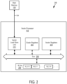
- FIG. 2 illustrates example parts of an example computing device 200, in accordance with some embodiments of the present disclosure.
- computing device 200 includes vector processor 102 as well as bus 104 and main memory 106 (e.g., see FIG. 1 ).
- Computing device 200 can also be or include computing device 100.
- vector processor 102 includes vector registers 202, scalar registers 204, bus 206, arithmetic logic units 208 (ALUs 208), and vector load-store unit 210.
- Other embodiments of the computing device 200 can include the scalar registers 204 being external to the vector processor 102 or in a separate unit of the vector processor from a unit in the vector processor having the vector registers 202.
- the bus 206 communicatively couples vector registers 202, scalar registers 204, arithmetic logic units (ALUs) 208, and vector load-store unit 210, and such components can communicate with each other via bus 206 (which can include multiple buses).
- Vector registers 202 include multiple vector registers.
- ALUs 208 include multiple ALUs--e.g., arithmetic logic unit (ALU) 0, ALU 1, and ALU N.
- Vector processor 102 includes at least one vector index register.
- Vector processor 102 can be or include one or more central processing units (CPUs) that implement instructions that operate on one-dimensional arrays of data called vectors.
- CPUs central processing units
- Vector registers 202 in the vector processor 102 can include operand vector registers (i.e., input vector registers), result vector registers (i.e., output vector registers), and vector index registers that store values used for accessing elements in operand vector registers and/or result vector registers.
- operand vector registers i.e., input vector registers
- result vector registers i.e., output vector registers
- vector index registers that store values used for accessing elements in operand vector registers and/or result vector registers.
- the values in the accessed elements of operand vector registers and/or result vector registers can be used as input for ALUs such as one or more of the ALUs 208.
- the vector processor 102 can include index registers that can include scalar index registers and vector index registers such as the vector index registers illustrated in FIGS. 5 and 8 .
- the scalar registers 204 of the vector processor 102 can include scalar index registers as well as operand scalar registers (i.e., input scalar registers) and result scalar resisters (i.e., output scalar registers). At least some of the scalar registers can provide indexing and control values for many different types of operations on scalars and vectors. Also, scalar registers can also provide numerical values used by the vector instructions. For example, a vector provided by a vector register can be multiplied by a scalar provided by a scalar register.
- At least some of the scalar registers 204 and the vector registers 202 can be connected to respective ALUs of the ALUs 208.
- An ALU of ALUs 208 can include a combinational digital electronic circuit that performs arithmetic and bitwise operations on integer binary numbers.
- an ALU of the ALUs 208 can be connected to input vector registers and in some instances output vector registers if the output vector register is providing feedback in an operation. In such instances the output vector register is both an input and output vector.
- the scalar registers 204 can include programable scalar registers.
- a programable scalar register can be used so that a vector provided by a vector register (e.g., one of the vector registers 202) can be operated on by a scalar provided by and programed into one of the programable scalar registers.
- one of the operations can include a vector multiplied by a scalar value (e.g., vector A(i) X scalar p).
- Vector load-store unit 210 includes circuitry for executing load and store instructions, generating addresses of load and store vector operations and loading data from memory or storing it back to memory from the registers of the vector processor 102.
- Vector load-store unit 210 can perform many of the operations described herein including many of the operations of methods 300, 400, and 600 in FIGS. 3 , 4 , and 6-7 .
- Each of the computing devices described herein can be a machine capable of executing a set of instructions (sequential or otherwise) that specify actions to be taken by that machine. Further, while a single machine is illustrated for each of the illustrated computing devices of FIGS. 1 and 2 , the term "machine" shall also be taken to include any collection of machines that individually or jointly execute a set (or multiple sets) of instructions to perform any one or more of the methodologies or operations discussed herein. And, each of the illustrated computing devices can each include at least a bus and/or motherboard, one or more controllers (such as one or more CPUs), a main memory that can include temporary data storage, at least one type of network interface, a storage system that can include permanent data storage, and/or any combination thereof.
- an operand vector register can be addressed using at least an index from a vector index register (VIR) or another type of register such as a counter register.
- VIR vector index register
- the counter adds 1 or another number to itself for each iteration or step in a DO or FOR loop that generates the address for the next iteration or step.
- the counter can add 2 or another number that is a multiple of two to itself for each iteration or step in a DO or FOR loop that generates the address for the next iteration or step.
- the counter can add 2 in dual lane processing.
- the number added to the current counter number for each increment of the counter number can depend on the number of lanes used by the vector processor. For example, the number added to the counter number can be equal to the number of lanes used. In systems 500 and 800, 2 is added to the count with each increment of the counter and two lanes are being used in both systems.
- the VIRs do not have to be driven by a counter, but it can be useful to have the VIRs driven by one or more counters.
- Common counters can both provide the address inputs to the VIRs and can provide a separate address input to a receiving multiplexor that outputs an address component for use in accessing an operand vector in a vector operation.
- B(i) A(VMX(i)
- B(i) A(VMX(i)
- the processor can do A +a, where "a" is a scaler from the counter via the multiplexor.
- the processor can do A(VMX) +a by using the addresses generated from the output of the VIR.
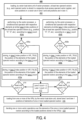
- FIGS. 3 and 4 each illustrates example multiple lane operations for two lanes for building indexing vectors for storing in vector indexing registers for TRUE and FALSE results (e.g., "0" and "1" results) of a conditional test operation (VIR_TRUE and VIR_FALSE), in accordance with some embodiments of the present disclosure.
- a conditional test operation VIR_TRUE and VIR_FALSE
- One example difference between the methods in FIGS. 3 and 4 is that the method 300 in FIG. 3 includes performing a conditional test operation with at least one operand scalar and at least one operand vector and the method 400 in FIG. 4 includes performing a conditional test operation with at least two operand vectors.
- the method 300 begins at step 302 with loading, by a vector load-store unit of a vector processor (e.g., see vector load-store unit 210), at least one operand vector and at least one operand scalar.
- each operand vector is stored in a respective dual-access operand vector register (e.g. see operand vector register 504 or 506 depicted in FIG 5 ).
- each scalar can be stored in a respective operand scalar register (e.g., see scalar registers 204).
- even positions in a vector are in a first lane and odd positions are in a second lane, or vice versa.
- the method 300 continues with performing, by the vector processor, a conditional test operation on the scalar(s) with an element at a first lane (lane 0) index position of the at least one operand vector (e.g., position "0", "2", etc.) according to a first lane count (lane 0 count).
- the first lane count can be stored in a first lane counter of the vector processor (e.g., see lane 0 counter 508a depicted in FIG. 5 ).
- the method 300 continues with performing, by the vector processor, a conditional test operation on the scalar(s) with an element at a second lane (lane 1) index position of the at least one operand vector (e.g., position "1", "3", etc.) according to a second lane count (lane 1 count).
- the second lane count can be stored in a second lane counter of the vector processor (e.g., see lane 1 counter 508b depicted in FIG. 5 ).
- the conditional test operation is performed on at least one scalar from a scalar register and elements of at least one of the loaded one or more operand vectors according to first and second lane counts stored in respective counters.
- the counters can be scalar registers and a part of the vector processor. No circuit is depicted in the drawings showing an operand scalar register and an operand vector register; however, it is to be understood that the system 500 depicted in FIG. 5 includes components that can support the method 300--except one of the operand vector registers (e.g., register 504 or 506) would be replaced with an operand scalar register.
- the method 300 continues with identifying, by the vector processor, whether the result of the conditional test operation in step 304a is a TRUE result. To put it another way, at step 306a, the method 300 continues with identifying whether the result of the conditional test operation of step 304a is TRUE or FALSE (e.g., Boolean "1" or "0").
- TRUE e.g., Boolean "1" or "0"
- step 308a the method 300 continues at step 308a with storing, in a first lane index position in a vector index register for TRUE results of the conditional test operation (VIR_TRUE), the position of the element(s) of the loaded operand vector(s) according to the first lane count (such as according to the first lane count via a first lane TRUE count stored in a first lane TRUE counter—e.g., see first lane TRUE counter 5160a depicted in FIG. 5 ).
- VIR_TRUE conditional test operation
- step 310a the method 300 continues at step 310a with storing, in a first lane index position in a vector index register for FALSE results of the comparison (VIR_FALSE), the position of the element(s) of the loaded operand vector(s) according to the first lane count (such as according to the first lane count via a first lane FALSE count stored in a first lane FALSE counter—e.g., see first lane FALSE counter 5160b depicted in FIG. 5 ).
- VIR_FALSE vector index register for FALSE results of the comparison
- the method 300 continues with identifying, by the vector processor, whether the result of the conditional test operation in step 304b is a TRUE result. To put it another way, at step 306b, the method 300 continues with identifying whether the result of the conditional test operation of step 304b is TRUE or FALSE (e.g., Boolean "1" or "0").
- TRUE e.g., Boolean "1" or "0"
- step 308b the method 300 continues at step 308b with storing, in a second lane index position in the VIR_TRUE, the position of the element(s) of the loaded operand vector(s) according to the second lane count (such as according to the second lane count via a second lane TRUE count stored in a second lane TRUE counter—e.g., see first lane TRUE counter 5161a depicted in FIG. 5 ).
- step 310b the method 300 continues at step 310b with storing, in a second lane index position in the VIR_FALSE, the position of the element(s) of the loaded operand vector(s) according to the second lane count (such as according to the second lane count via a second lane FALSE count stored in a second lane FALSE counter—e.g., see second lane FALSE counter 5161b depicted in FIG. 5 ).
- the first lane count and the second lane count are each incremented by two.
- the method 300 repeats steps 304a, 304b, 306a, 306b, 308a, 308b, 310a, 310b, and 312 until either of the first count or the second count equals or exceeds the vector length (VL) of at least one of the operand vector(s).
- VL vector length
- the vector processor can continue with storing positions of elements of the loaded operand vector(s) according to the counts until the positions of the elements of the loaded operand vector(s) are stored in the VIR_TRUE or the VIR_FALSE.
- the method 300 continues the storing of positions of elements of the loaded operand vector(s) according to the counts until the positions of the elements of the loaded operand vector(s) are stored in the VIR_TRUE or the VIR_FALSE.
- the method 300 continues with identifying whether the first lane count or the second lane count equals or exceeds the VL of at least one of the operand vector(s). In some embodiments, the method 300 can continue with identifying whether the VL of one of the OVR(s), accessed by the conditional test operation, equals the result of adding the VL of the VIR_TRUE and the VL of the VIR_FALSE, which can be another way to identify whether one of the counts equals or exceeds the VL of the operand vector(s) stored in the OVR(s). These example alternative ways of identifying whether the count equals the VL of at least one of the operand vector(s) can show that all the elements of an OVR accessed by the test operation are used in the conditional test operation.
- the method continues at steps 304a and 304b. Otherwise, the method 300 has completed the building of indexing vectors for storing in VIR_TRUE and VIR_FALSE.
- the method 300 Upon completion of the building of indexing vectors which are stored in VIR_TRUE and VIR_FALSE, the method 300 continues, at step 316, with loading from VIR_TRUE and/or VIR_FALSE, by the vector load-store unit, stored first lane and second positions of elements of one or more loaded operand vectors. And, at step 318, the method 300 continues with iterating one or more vector operations over the elements of the loaded operand vector(s) according to the loaded positions stored in the VIR_TRUE and/or VIR_FALSE. In some embodiments, the number of iterations for step 318 is equal to the VL (as shown in step 312).
- two respective registers can be loaded with the new vector lengths for VIR_TRUE and VIR_FALSE (e.g., VL_VIR_TRUE and VL_VIR_FALSE).
- VL_VIR_TRUE and VL_VIR_FALSE e.g., VL_VIR_TRUE and VL_VIR_FALSE.
- respective VL registers can be loaded with vector lengths of the OVRs as well.
- the vector processor can determine the number of iterations on the OVR(s) and/or the VIRs according to their respective VL values in respective VL registers.
- Methods 300 and 400 in FIGS. 3 and 4 are somewhat similar except for some minor differences. As mentioned herein, one example difference between the methods in FIGS. 3 and 4 is that the method 300 in FIG. 3 includes performing a conditional test operation with at least one operand scalar and at least one vector operand and the method 400 in FIG. 4 includes performing a conditional test operation with at least two operand vectors.
- the method 400 begins at step 402 with loading, by a vector load-store unit of vector processor, at least two operand vectors.
- each operand vector is stored in a respective dual-access operand vector register (e.g. see operand vector register 504 or 506 depicted in FIG 5 ).
- a dual-access operand vector register e.g. see operand vector register 504 or 506 depicted in FIG 5 .
- even positions in a vector are in a first lane and odd positions are in a second lane, or vice versa.
- the method 400 continues with performing, by the vector processor, a conditional test operation with respective elements at similar first lane (lane 0) index positions of the at least two operand vectors (e.g., position "0", "2", etc.) according to a first lane count.
- the first lane count can be stored in a first lane counter of the vector processor (e.g., see lane 0 counter 508a depicted in FIG. 5 ).
- the method 400 continues with performing, by the vector processor, a conditional test operation with respective elements at similar second lane (lane 1) index positions of the at least two operand vectors (e.g., position "0", "2”, etc.) according to a second lane count.
- the second lane count can be stored in a second lane counter of the vector processor (e.g., see lane 1 counter 508b depicted in FIG. 5 ).
- the method 400 continues with identifying, by the vector processor, whether the result of the conditional test operation in step 404a is a TRUE result. If the result of the operation at step 404a is TRUE, then the method 400 continues at step 408a with storing, in a first lane index position in VIR_TRUE, the position of the elements of the loaded operand vectors according to the first lane count (such as according to the first lane count via a first lane TRUE count stored in a first lane TRUE counter—e.g., see first lane TRUE counter 5160a depicted in FIG. 5 ).
- step 410a the method 400 continues at step 410a with storing, in a first lane index position in VIR_FALSE, the position of the elements of the loaded operand vectors according to the first lane count (such as according to the first lane count via a first lane FALSE count stored in a first lane FALSE counter—e.g., see first lane FALSE counter 5160b depicted in FIG. 5 ).
- the method 400 continues with identifying, by the vector processor, whether the result of the conditional test operation in step 404b is a TRUE result. If the result of the operation at step 404b is TRUE, then the method 400 continues at step 408b with storing, in a second lane index position in VIR_TRUE, the position of the elements of the loaded operand vectors according to the second lane count (such as according to the second lane count via a second lane TRUE count stored in a second lane TRUE counter—e.g., see second lane TRUE counter 5161a depicted in FIG. 5 ).
- step 410b the method 400 continues at step 410b with storing, in a second lane index position in VIR_FALSE, the position of the elements of the loaded operand vectors according to the second lane count (such as according to the second lane count via a second lane FALSE count stored in a second lane FALSE counter—e.g., see second lane FALSE counter 5161b depicted in FIG. 5 ).
- the first lane count and the second lane count are each incremented by two.
- the method 400 repeats steps 404a, 404b, 406a, 406b, 408a, 408b, 410a, 410b, and 412 until either of the first count or the second count equals or exceeds the vector length (VL) of at least one of the operand vectors.
- VL vector length
- the vector processor can continue with storing positions of elements of the loaded operand vectors according to the counts until the positions of the elements of the loaded operand vectors are stored in the VIR_TRUE or the VIR_FALSE.
- the method 400 continues with identifying whether the first lane count or the second lane count equals or exceeds the VL of at least one of the operand vectors. In some embodiments, the method 400 can continue with identifying whether the VL of one of the OVRs, accessed by the conditional test operation, equals the result of adding the VL of the VIR_TRUE and the VL of the VIR_FALSE. If the first count and the second count are both less than the VL of one of the operand vectors, then the method continues at steps 404a and 404b. Otherwise, the method 400 has completed the building of indexing vectors for storing in VIR_TRUE and VIR_FALSE.
- the method 400 Upon completion of the building of indexing vectors which are stored in VIR_TRUE and VIR_FALSE, the method 400 continues, at step 416, with loading from VIR_TRUE and/or VIR_FALSE, by the vector load-store unit, stored first lane and second positions of elements of one or more loaded operand vectors. And, at step 418, the method 400 continues with iterating one or more vector operations over the elements of the loaded operand vector(s) according to the loaded positions stored in the VIR_TRUE and/or VIR_FALSE.
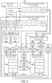
- FIG. 5 illustrates an example system 500 for building indexing vectors for storing in VIR_TRUE 502a and VIR_FALSE 502b, in accordance with some embodiments of the present disclosure.
- the system 500 can implement many of the operations and aspects of methods 300 and 400 and the system 500 can be a part of one or more vector processors.
- the system 500 includes the VIR_TRUE 502a and VIR_FALSE 502b.
- the system also includes a first OVR 504 and a second OVR 506, such as OVRs mentioned in the description of method 400.
- the system 500 also includes a first lane counter 508a, which can be partially implemented by a counter register and can be the first lane counter described in the description of the method 400.
- the system 500 also includes a second lane counter 508b, which can be partially implemented by a counter register and can be the second lane counter described in the description of the method 400.
- the system 500 also includes a first lane conditional test operation 5100 that can perform a conditional test operation, such as a comparison of the values stored in the first lane of first and second OVRs 504 and 506.
- the system 500 also includes a second lane conditional test operation 5101 that can perform a conditional test operation, such as a comparison of the values stored in the second lane of the first and second OVRs 504 and 506.
- the first lane conditional test operation 5100 can execute against elements of two vectors having a similar address (e.g., a similar index or iteration i), in a first lane, one test or comparison at a time or per cycle.
- a similar address e.g., a similar index or iteration i
- the first lane counter 508a provides address i for accessing the OVRs 504 and 506 for the first lane conditional test operation 5100.
- the index "i" for the first lane is incremented by two.
- the elements/outputs of OVRs 504 and 506 at iteration or address i are compared to each other or with a value from another register such as a scalar register (e.g., see method 300).
- the first lane conditional test operation 5100 generates a single output, which is either TRUE or FALSE (e.g., "1" or "0").
- the second lane conditional test operation 5101 can execute against elements of two vectors having a similar address (e.g., a similar index or iteration j), in a second lane, one test or comparison at a time or per cycle.
- a similar address e.g., a similar index or iteration j
- the second lane counter 508b provides address j for accessing the OVRs 504 and 506 for the second lane conditional test operation 5101.
- the index "j" for the second lane is incremented by two.
- the elements/outputs of OVRs 504 and 506 at iteration or address j are compared to each other or with a value from another register such as a scalar register (e.g., see method 300).
- the second lane conditional test operation 5101 generates a single output, which is either TRUE or FALSE (e.g., "1" or "0").
- the conditional test operations 5100 and 5101 can be configured to perform the test operations at steps 304a and 304b respectively or can be configured to perform the test operations at steps 404a and 404b respectively.
- the first and second lane conditional test operations 5100 and 5101 can be configured to execute on elements of the loaded operand vectors according to respective counts stored in respective counter registers such counters 508a and 508b.
- the conditional test operations 5100 and 5101 can also be configured to perform the identification of a TRUE or FALSE result at steps 306a or step 306b respectively or at steps 406a or step 406b respectively.
- the conditional test operations 5100 and 5101 can be configured to identify whether the result of the conditional test operations are TRUE or FALSE.
- the conditional test operations 5100 and 5101 can be configured to output a TRUE or FALSE result, such as a "1" for a TRUE result or a "0" for a FALSE result.
- the output of each of the conditional test operations 5100 and 5101 is inputted into a respective write enable for each of the VIR_TRUE 502a and the VIR_FALSE 502b (e.g., see write enables 5120a, 5120b, 5121a, and 5121b).
- the system 500 includes write enable 5120a for first lane positions of VIR_TRUE 502a, write enable 5120b for first lane positions of VIR_FALSE 502b, write enable 5121a for second lane positions of VIR_TRUE 502a, and write enable 5121b for second lane positions of VIR_FALSE 502b.
- the output from the first lane conditional test operation 5100 can be communicated directly to the write enable 5120a for the VIR_TRUE 502a.
- the output from the first lane conditional test operation 5100 can be communicated indirectly to the write enable 5120b for the VIR_FALSE 502b, via an inverter 5140.
- the inverter 5140 is configured to invert the output of first lane conditional test operation 5100 before it reaches the write enable 5120b for the VIR_FALSE 502b.
- the inverter 5140 Inverts the value to FALSE (e.g., "0") and outputs FALSE.
- the output from the second lane conditional test operation 5101 can be communicated directly to the write enable 5121a for the VIR_TRUE 502a.
- the output from the second lane conditional test operation 5101 can be communicated indirectly to the write enable 5121b for the VIR_FALSE 502b, via an inverter 5141.
- the inverter 5141 is configured to invert the output of second lane conditional test operation 5101 before it reaches the write enable 5121b for the VIR_FALSE 502b.
- the system 500 also includes separate TRUE counters 5160a and 5160b for the first and second lanes of the VIR_TRUE 502a and separate FALSE counters 5161a and 5161b for the VIR_FALSE 502b.
- the outputs of the conditional test operations 5100 and 5101 drive the four counters, counters 5160a, 5160b, 5161a and 5161b.
- the counters 5160a, 5160b, 5161a and 5161b are separate from the first and second lane counters 508a and 508b that provide the addresses i and j for the OVRs 504 and 506.
- Outputs of TRUE counters 5160a and 5161a are used as the first and second lane addresses for accessing VIR_TRUE 502a.
- Outputs of FALSE counters 5160b and 5161b are used as the first and second lane addresses for accessing VIR_FALSE 502b.
- the output triggers write enable 5120a to write the current first lane position of the OVRs 504 and 506 into the VIR_TRUE 502a.
- the output triggers write enable 5120b to write the current first lane position from the OVRs 504 and 506 into the VIR_FALSE 502b.
- This functionality is provided via the circuit including the inverter 5140 and the two write enables 5120a and 5120b.
- somewhat similar functionality can be provided for the second lane positions of the OVRs 504 and 506 via the circuit including the inverter 5141 and the two write enables 5121a and 5121b.
- the outputs of counters 2508a and 2508b are also used as the addresses or address components (or indexes) to be written into VIR_TRUE 502a at addresses specified by the first lane TRUE counter 5160a and the second lane TRUE counter 5161a. This occurs when the output of the test operations 5100 and 5101 are TRUE.
- the respective values stored in TRUE counters 5160a and 5161a are increased by two for each triggering TRUE output from the test operations 5100 and 5101 respectively.
- the output of 508a and 508b are also used as the addresses or address components to be written into VIR_FALSE 502b at addresses specified by the first lane FALSE counter 5160b and the second lane FALSE counter 5161b.
- the VIR_TRUE 502a and the VIR_FALSE 502b each are an output register of the system 500.
- the system 500 can be a part of a vector processor that includes a vector load-store unit, such as the vector processor in FIG. 2 .
- the system 500 is also shown to include a scalar register for vector length, vector length register 524 (VLR 524).
- VLR 524 is configured to store the vector length (VL) of the OVRs 504 and 506.
- a vector processor can load the VL into memory from VLR 524 to identify whether the count from one of counters 508a and 508b equals the VL of the respective operand vectors stored in the OVRs 504 and 506. In other words, one value is in a register for the VL of the operand vectors in OVRs 504 and 506. This is one way for example to implement step 314 of method 300 or 414 of method 400.
- the counts in the counters continue to increment per clock cycle or another trigger or iteration (e.g., see steps 312 or 412).
- the vector processor can continue with storing positions of elements of the OVRs 504 and 506 until the positions of the elements of the OVRs are stored in the VIR_TRUE 502a or the VIR_FALSE 502b. If one of the counts is equal to or exceeds the VL, then the vector processor using system 500 has completed the building of indexing vectors for storing in VIR_TRUE 502a and VIR_FALSE 502b.
- the count is reset in the counters 508a and 508b (as well as the TRUE and FALSE counters) and VL is determined and stored in VLR 524.
- the vector processor can initially determine the vector length of an OVR (e.g., the lengths of the OVRs 504 and 506) and then store the lengths (which is one length) in the VLR 524 before performing method 300 or 400.
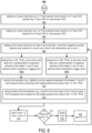
- FIGS. 6 and 7 illustrate example operations of method 600 for executing operations on elements of operand vectors using multiple lanes and according to a VIR_TRUE and a VIR_FALSE (e.g., see VIR_TRUE 802a and VIR_FALSE 802b depicted in FIG. 8 ), in accordance with some embodiments of the present disclosure.
- the example operations of method 600 for executing operations on elements of operand vectors can be according to a VIR_TRUE and a VIR_FALSE that are accessed in parallel in that, for example, both occurrences of position i in VIR_TRUE and VIR_FALSE are accessed in the same clock cycle or iteration (not depicted), in accordance with some embodiments of the present disclosure.
- vector lengths of VIR_TRUE and VIR_FALSE, VL_VIR_TRUE and VL_VIR_FALSE are not compared to the count and the count is not reset during the executing of the operations on the operand vectors.
- step 616 can occur per clock cycle or iteration of the operations.
- steps 606-612 and steps 620-626 can be performed in parallel as well.
- the method 600 begins at step 602, with loading, by a vector load-store unit, a first input operand vector stored in a first input OVR (e.g., see first OVR 804a).
- the first input OVR can be a dual-access OVR.
- the method 2100 continues with loading, by a vector load-store unit, a second input operand vector stored in a second input OVR (e.g., see second OVR 804b).
- the second input OVR can be a dual-access OVR.
- the method 600 continues with loading, by the vector load-store unit, a first lane count and a second lane count from respective counters (e.g., see first and second lane counters 808a and 808b). In some embodiments, even numbered positions in a vector are in the first lane and odd numbered positions are in the second lane).
- the method 600 continues with loading from a VIR_TRUE, by the vector load-store unit, a stored position of respective elements of the loaded first and second input operand vectors according to the first lane count.
- the method 600 continues with loading from the VIR_TRUE, by the vector load-store unit, a stored position of respective elements of the loaded first and second input operand vectors according to the second lane count. As shown in FIG. 6 , steps 608a and 608b can performed in parallel or simultaneously.
- Step 610 the method 600 continues with executing a first operation (e.g., addition) over the respective elements of the loaded first and second input operand vectors according to the loaded positions from the first and second lanes in the VIR_TRUE.
- Step 610 includes step 612 that includes the method 600 continuing with storing the result of the first operation (e.g., result from ALUs for first and second lanes-see first lane ALU 814a and second lane ALU 814b) into an output OVR (e.g., see output OVR 810) at positions that correspond to the loaded positions from the first and second lanes in VIR_TRUE.
- a first operation e.g., addition
- the method 600 continues with incrementing each of the first and second lane counts by two.
- the method 600 continues with comparing the first and second lane counts to a value representing the vector length of the VIR_TRUE, i.e., VL_VIR_TRUE, such that the first operation can be iterated over the loaded first and second input operand vectors stored in the input operand vector registers for each of the positions stored in the VIR_TRUE.
- VL_VIR_TRUE the vector length of the VIR_TRUE
- VL_VIR_TRUE and the VL_VIR_FALSE are preloaded with the vector lengths of VIR_TRUE and VIR_FALSE before the method 600 is initiated.
- the VL_VIR_TRUE and the VL_VIR_FALSE are loaded with the lengths of the vectors in VIR_TRUE and the VIR_FALSE while VIR_TRUE and VIR_FALSE are loaded with vector index elements.
- step 616 the method 600 continues with returning to step 606 (loading the first and second lane counts) which is followed by steps 608a and 608b (loading stored positions from the VIR_TRUE) and step 610 (running the first operation over the elements of the loaded input operand vectors). This way the first operation is iterated over the input OVRs for each of the first and second lane positions stored in the VIR_TRUE.
- the method 600 continues with loading, by the vector load-store unit, the first and second lane counts stored in the respective counter registers.
- the value of the first lane count at the first iteration of step 620 can be "0" and the value of the second lane count at the first iteration of step 620 can be "1".
- the counts are incremented by two, so in such examples the next value of the first lane count can be "2", and the next value of the second lane count can be "3".
- the method 600 continues with loading from a VIR_FALSE, by the vector load-store unit, a stored position of respective elements of the loaded first and second input operand vectors according to the first lane count.
- the method 600 continues with loading from a VIR_FALSE, by the vector load-store unit, a stored position of respective elements of the loaded first and second input operand vectors according to the second lane count.
- Step 624 the method 600 continues with executing a second operation (e.g., subtraction) over the respective elements of the loaded first and second input operand vectors according to the loaded positions from first and second lanes in VIR_FALSE.
- Step 624 includes step 626 that includes the method 600 continuing with storing results of the second operation (e.g., results from respective ALUs for first and second lanes) into the output OVR at positions that correspond to the loaded positions from first and second lanes in VIR_FALSE.
- results of the second operation e.g., results from respective ALUs for first and second lanes
- the method 600 continues with incrementing each of the first and second lanes counts by two.
- the method 600 continues with comparing the counts to a value representing the vector length of the VIR_FALSE, i.e., VL_VIR_FALSE, such that the first operation can be iterated over the loaded first and second input operand vectors stored in the input operand vector registers for each of the positions stored in the VIR_FALSE.
- VL_VIR_FALSE the vector length of the VIR_FALSE
- step 630 the method 600 continues with returning to step 620 (loading the counts) which is followed by steps 622a and 622b (loading positions from the VIR_FALSE) and step 624 (running the second operation over the elements of the loaded input operand vectors). This way the second operation is iterated over the input OVRs for each of the first and second lane positions stored in the VIR_FALSE.
- the first operation can include addition, subtraction, multiplication, division, or any other type of operation that can be performed by one or more ALUs.
- the second operation can include a different operation from the first operation that can be performed by one or more ALUs.
- FIG. 8 illustrates an example system 800 including VIR_TRUE 802a and VIR_FALSE 802b being used for executing, in multiple lanes, first and second operations on elements of input operand vectors stored in input operand vector registers 804a and 804b, in accordance with some embodiments of the present disclosure.
- Example system 800 is one example of a system that can implement at least method 600.
- VIR_TRUE 802a and VIR_FALSE 802b are dual-access VIRs. Thus, two addresses in each of the VIRs can be accessed in parallel (e.g., in one clock cycle). As shown, an address "i" and an address "j" from a first lane counter and a second lane counter respectively can be inputs into both the dual-access VIRs. Also, the VIR_TRUE 802a and VIR_FALSE 802b each can output a stored first lane element and a stored second lane element in parallel (e.g., in one clock cycle).
- the system 800 also includes input OVRs 804a and 804b.
- the input OVRs are dual-access OVRs in the system 800.
- the system 800 also includes an output operand register 810 which is also a dual-access OVR.
- the first and second lane ALUs 814a and 814b can receive first lane and second lane inputs from the input OVRs 804a and 804b and output results of numerical operations performed by the ALUs to the output OVR 810.
- the system 800 also includes first lane counter 806a which outputs index "i" and second lane counter which outputs index "j".
- Index i can be used as the first lane count in method 600.
- Index j can be used as the second lane count in method 600.
- the system 800 also includes first lane multiplexor 808a and second lane multiplexor 808b.
- Each of the multiplexors 808a and 808b can execute in a regular mode, a TRUE mode, and a FALSE mode.
- the multiplexors 808a and 808b allow for the switching of TRUE mode to FALSE mode after the resetting of first and second lane counters in method 600.
- the first lane multiplexor 808a receives input from the first lane counter 806a, the first lane of VIR_TRUE 802a, and the first lane of VIR_FALSE 802b.
- the multiplexor 808a outputs one of the three inputs depending on its mode.
- the second lane multiplexor 808b receives input from the second lane counter 806b, the second lane of VIR_TRUE 802a, and the second lane of VIR_FALSE 802b.
- the multiplexor 808b outputs one of the three inputs depending on its mode.
- the system 800 also includes registers for vectors lengths of the VIR_TRUE 802a and the VIR FALSE 802b.
- the vector lengths can be used at steps 616 and 630 respectively in method 600.
- the system 800 also includes ALUs for each lane in dual-lane processing (e.g., first lane ALU 814a and second lane ALU 814b).
- the ALUs 814a and 814b can perform subtraction, multiplication, division, or any other type of operation that can be performed by one or more ALUs according to the opcodes (e.g., opcodes 816a and 816b) received via the multiplexor 818.
- the output of the multiplexor 818 can be received by both of the ALUs 814a and 814b.
- the VIR_TRUE 802a stores a list of positions of the input OVRs 804a and 804b. For example, “1" is stored in position "0" of VIR_TRUE 802a, which can be used as an address for accessing position "1" in both input OVRs 804a and 804b.
- position "0" of the VIR_TRUE as well as positions "2", "4", etc. are in a first lane of the VIR_TRUE.
- the other positions of VIR_TRUE are in a second lane of VIR_TRUE.
- the VIR_FALSE 802b stores a list of positions of the input OVRs 804a and 804b.
- positions "0" and “2" are stored in positions “0" and “1" of VIR_FALSE 802b respectively, which can be used as addresses for accessing positions “0” and “2” in both input OVRs 804a and 804b.
- position "0" of the VIR_FALSE as well as positions "2", "4", etc. are in a first lane of the VIR_FALSE.
- the other positions of VIR_FALSE are in a second lane of VIR_FALSE.
- the vector processor executes for at least two iterations of a subtraction operation and for at least one iteration of an addition operation.
- counter 806a At the first iteration of the at least two cycles of the subtraction operation, counter 806a outputs the count of "0" which is the value stored in the counter at the first cycle during a subtraction mode.
- VIR_FALSE 802b In the first cycle of the subtraction mode, VIR_FALSE 802b is shown outputting selected address "0" from position "0" of the VIR_FALSE.
- counter 806a outputs the count of "0" as well, which is the value stored in the counter at the first cycle during an addition mode.
- VIR_TRUE 802a In the first cycle of the addition mode, VIR_TRUE 802a is shown outputting selected address "1" from position "0" of the VIR_TRUE. Being that position "0" in both of the VIRs is a first lane position and the OVRs are dual access OVRs, the subtraction and addition can occur within a first lane within a first clock cycle in parallel.
- the first lane multiplexor 808a selects between the address component ("0") as specified by the counter 806a in a NORMAL mode operation or the address component ("1") as stored in position "0" of the VIR_TRUE 802a in a TRUE mode of operation or the address component ("0") as stored in position "0" of the VIR_FALSE 802b in a FALSE mode of operation.
- position "0" is a first lane position in the example; thus, the first lane multiplexor 808a is used.
- second lane multiplexor 808b selects between the address component ("1") as specified by the counter in the NORMAL mode operation or the address component ("5") as stored in position "1" of the VIR_TRUE 802a in the TRUE mode of operation or the address component ("2") as stored in position "1" of the VIR_FALSE 802b in the FALSE mode of operation; and, so on.
- position "1" is a second lane position in the example; thus, the second lane multiplexor 808b is used.
- the first and second lane multiplexors 808a and 808b select between the outputs of counters 806a and 808b respectively, first and second lanes in VIR_TRUE 802a respectively, and first and second lanes in VIR_FALSE 802b respectively.
- the outputs provided by the first lane in VIR_TRUE 802a and VIR_FALSE 802b are according to the count of the first lane counter 806a.
- the outputs provided by the second lane in VIR_TRUE 802a and VIR_FALSE 802b are according to the count of the second lane counter 806b.
- the multiplexors 808a and 808b can implement a switching from the TRUE mode to the FALSE mode upon the reset of the counters at step 618.
- the counters 806a and 806b are reset when one of the counts equals or exceeds the vector length of either the VIR_TRUE or the VIR_FALSE (e.g., see VL_VIR_TRUE 812a and VL_VIR_FALSE 812b). This switching allows for the loop of steps 606-616 to switch to the loop of steps 620-630.
- selections described herein can be according to programmer visible instructions and/or can be a hardwired circuit that is doing some a high level semantic operation.
- the output of "1" from the VIR_TRUE 802a is the address component used for accessing the input OVRs 804a and 804b.
- the input OVRs 804a and 804b are accessed for respective outputs of element “30" at position "1" of the input OVR 804a and element “25” at position "1" of input OVR 804b.
- the output OVR 810 (or the third OVR) is addressed as well at position "1".
- the position "1" is outputted by the first lane multiplexor 808a which has been selected for TRUE mode in this example.
- the second lane ALU 814b performs an addition operation since position "1" in the OVRs is a second lane position for the OVRs.
- first lane positions of the OVRs are positions "0", “2", “4", etc.
- the second lane positions of the OVRs are positions "1", "3", "5", etc.
- the addition operation is according to the first opcode 816a which is selected by the multiplexor 818 in the TRUE mode.
- the output of "0" from the VIR_FALSE 802a is the address component used for accessing the input OVRs 804a and 804b.
- the input OVRs 804a and 804b are accessed for respective outputs of element “10" at position "0" of the input OVR 804a and element “20" at position "0" of input OVR 804b.
- position "0" in this example is a first lane position.
- the output OVR 810 (or the third OVR) is addressed as well at position "0".
- the position "0" is outputted by the first lane multiplexor 808a which has been selected for FALSE mode in this example. Also, in the FALSE mode the first lane ALU 814a performs subtraction operation, since position "0" in the OVRs is a first lane position for the OVRs. The subtraction operation is according to the second opcode 816b which is selected by the multiplexor 818 in the FALSE mode. The output of the opcode is output 819 which can be inputted into both the first lane and the second lane ALUs 814a and 814b.
- the elements of input OVRs 804a and 804b at position "0" are inputted into the first lane ALU 814a.
- the first lane ALU 814a subtracts the element of position "0" of OVR 804b from the element of position "0" of OVR 804a, and outputs the result of the subtraction operation.
- the addition and subtraction operations illustrated in FIG. 8 are merely examples and that various operations can be performed on OVRs 804a and 804b according to the addressing by the VIRs 802a and 802b.
- the first opcode 816a can be an opcode for any arithmetic operation of an ALU
- the second opcode 816b can be an opcode for any arithmetic operation of an ALU as well.
- the system 800 can implement method 600.
- each vector of the one or more operand vectors can be stored in OVRs 804a and 804b.
- the counts can be stored in respective first and second lane counters 806a and 806b.
- the positions can be store in VIRs 802a and 802b.
- the executing of the first and the second operations in two lanes in steps 610 and 624 can be implemented by a combination of the OVRs, the VIRs, the multiplexors, and the ALUs depicted in FIG. 8 .
- the storage of the results of the operations in two lanes (at steps 612 and 626) can occur at the output OVR 810.
- the loops in the method 600 can be controlled according to at least the lengths stored in the registers 812a and 812b.
- the methods 300, 400, and 600 include just some of the many operations that can be implemented by the vector processors and systems described herein.
- the present disclosure also relates to an apparatus for performing the operations herein.
- This apparatus can be specially constructed for the intended purposes, or it can include a computer selectively activated or reconfigured by a computer program stored in the computer.
- a computer program can be stored in a computer readable storage medium, such as, but not limited to, any type of disk including floppy disks, optical disks, CD-ROMs, and magnetic-optical disks, read-only memories (ROMs), random access memories (RAMs), EPROMs, EEPROMs, magnetic or optical cards, or any type of media suitable for storing electronic instructions, each coupled to a computer system bus.
- the present disclosure can be partially provided as a computer program product, or software, that can include a machine-readable medium having stored thereon instructions, which can be used to program a computer system (or other electronic devices) to perform a process according to the present disclosure.
- a machine-readable medium includes any mechanism for storing information in a form readable by a machine (e.g., a computer).
- a machine-readable (e.g., computer-readable) medium includes a machine (e.g., a computer) readable storage medium such as a read only memory (“ROM”), random access memory (“RAM”), magnetic disk storage media, optical storage media, flash memory components, etc.
Landscapes
- Engineering & Computer Science (AREA)
- Theoretical Computer Science (AREA)
- Software Systems (AREA)
- Physics & Mathematics (AREA)
- General Engineering & Computer Science (AREA)
- General Physics & Mathematics (AREA)
- Computer Hardware Design (AREA)
- Quality & Reliability (AREA)
- Mathematical Physics (AREA)
- Computational Mathematics (AREA)
- Pure & Applied Mathematics (AREA)
- Mathematical Optimization (AREA)
- Mathematical Analysis (AREA)
- Computing Systems (AREA)
- Advance Control (AREA)
Claims (14)
- Procédé, comprenant :charger, par une unité de chargement-stockage vectorielle (210) d'un processeur vectoriel (102), un ou plusieurs vecteurs d'opérande, chaque vecteur de l'un ou de plusieurs vecteurs d'opérande étant stocké dans un registre vectoriel d'opérande respectif ;exécuter, par le processeur vectoriel (102), une opération de test conditionnel sur chaque élément à une première adresse d'au moins un vecteur parmi un ouplusieurs vecteurs d'opérande chargés selon un compte de la première voie stocké dans un premier registre de compteur de voies, les opérations de test conditionnel fournissant un vecteur de résultats de test ;stocker, dans une première position d'un premier registre d'indices vectoriels pour chaque résultat vrai des résultats vrais de l'opération de test conditionnel, une position du résultat vrai dans le vecteur de résultats de test selon le compte de la première voie ;stocker, dans une première position dans un deuxième registre d'indices vectoriels pour chaque résultat faux de résultats faux de l'opération de test conditionnel, une position du résultat faux dans le vecteur de résultats de test selon le compte de la première voie ;effectuer, par le processeur vectoriel (102), l'opération de test conditionnel sur chaque élément à une deuxième adresse d'au moins un vecteur parmi un ou plusieurs vecteurs d'opérande chargés, selon un compte de la deuxième voie stocké dans un deuxième registre de compteur de voies ;stocker, dans une deuxième position dans le premier registre d'indices vectoriels, une position du résultat vrai dans le vecteur de résultats de test selon le compte de la deuxième voie ; etstocker, dans une deuxième position dans le deuxième registre d'indices vectoriels, une position du résultat faux dans le vecteur de résultats de test selon le compte de la deuxième voie.
- Procédé selon la revendication 1, dans lequel les positions paires dans chaque vecteur d'opérande se trouvent dans la première voie et les positions impaires de chaque vecteur d'opérande se trouvent dans la deuxième voie.
- Procédé selon la revendication 1, dans lequel chaque registre vectoriel d'opérande respectif est accessible à la fois au registre de compteur de la première voie et au registre de compteur de la deuxième voie.
- Procédé selon la revendication 1, comprenant de plus :effectuer une première opération vectorielle sur les premiers éléments dans l'un ou plusieurs vecteurs d'opérande, les premiers éléments étant identifiés par des positions stockées dans le premier registre d'indices vectoriels ; eteffectuer une deuxième opération vectorielle sur les deuxièmes éléments dans l'un ou plusieurs vecteurs d'opérande, les deuxièmes éléments étant identifiés par des positions stockées dans le deuxième registre d'indices vectoriels.
- Procédé selon la revendication 1, comprenant de plus :charger, par l'unité de chargement-stockage vectorielle, un premier vecteur d'opérande d'entrée stocké dans un premier registre vectoriel d'opérande d'entrée ;charger, par l'unité de chargement-stockage vectorielle, un deuxième vecteur d'opérande d'entrée stocké dans un deuxième registre vectoriel d'opérande d'entrée ;charger, par l'unité de chargement-stockage vectorielle, à partir du premier registre d'indices vectoriels, une position stockée des éléments respectifs des premier et deuxième vecteurs d'opérande d'entrée chargés, selon le compte de la première voie ;charger, par l'unité de chargement-stockage vectorielle, à partir du premier registre d'indices vectoriels, une position stockée des éléments respectifs des premier et deuxième vecteurs d'opérande d'entrée chargés, selon le compte de la deuxième voie ; etexécuter une première opération sur les éléments respectifs des premier et deuxième vecteurs d'opérande d'entrée chargés, selon les positions chargées à partir de la première voie et de la deuxième voie dans le premier registre d'indices vectoriels.
- Procédé selon la revendication 5, dans lequel le premier registre vectoriel d'opérande d'entrée est accessible à la fois au registre de compteurs de la première voie et au registre de compteurs de la deuxième voie, et dans lequel le deuxième registre vectoriel d'opérande d'entrée est accessible à la fois au registre de compteurs de la première voie et au registre de compteurs de la deuxième voie.
- Procédé selon la revendication 5, comprenant de plus le stockage du résultat de la première opération dans un registre vectoriel d'opérande de sortie à des positions qui correspondent aux positions chargées à partir des première et deuxième voies dans le premier registre d'indices vectoriels.
- Procédé selon la revendication 7, comprenant de plus :continuer à exécuter la première opération sur les éléments respectifs des premier et deuxième vecteurs d'opérande d'entrée chargés selon les positions chargées à partir de la première voie et de la deuxième voie dans le premier registre d'indices vectoriels et à stocker les résultats de la première opération dans le registre vectoriel d'opérande de sortie aux positions correspondantes qui correspondent aux positions chargées à partir du premier registre d'indices vectoriels,jusqu'à ce que le compte de la première voie ou le compte de la deuxième voie dépasse ou égale la longueur du premier registre d'indices vectoriels ; etréinitialiser le compte e la première voie et le compte de la deuxième voie lorsque le compte de la première voie ou le compte de la deuxième voie dépasse ou égale la longueur du premier registre d'indices vectoriels.
- Procédé selon la revendication 8, dans lequel le compte de la première voie et le compte de la deuxième voie sont chacun incrémentés de deux par position chargée à partir du premier registre d'indices vectoriels.
- Procédé selon la revendication 8, comprenant de plus :
à la suite de la réinitialisation du compte de la première voie et du compte de la deuxième voie :charger, par l'unité de chargement-stockage vectorielle, à partir du deuxième registre d'indices vectoriels, une position stockée des éléments respectifs des premier et deuxième vecteurs d'opérande d'entrée chargés, selon le compte e la première voie ; etcharger, par l'unité de chargement-stockage vectorielle, à partir du deuxième registre d'indices vectoriels, une position stockée des éléments respectifs des premier etdeuxième vecteurs d'opérande d'entrée chargés, selon le compte de la deuxième voie ; etexécuter une deuxième opération sur les éléments respectifs des premier et deuxième vecteurs d'opérande d'entrée chargés selon les positions chargées à partir de la première voie et de la deuxième voie dans le deuxième registre d'indices vectoriels. - Procédé selon la revendication 10, comprenant de plus :
continuer à exécuter la deuxième opération sur les éléments respectifs des premier et deuxième vecteurs d'opérande d'entrée chargés selon les positions chargées à partir de la première voie et de la deuxième voie dans le deuxième registre d'indices vectoriels et à stocker les résultats de la première opération dans le registre vectoriel d'opérande de sortie aux positions correspondantes qui correspondent aux positions chargées à partir du deuxième registre d'indices vectoriels, jusqu'à ce que le compte de la première voie ou le compte de la deuxième voie dépasse ou égale la longueur du deuxième registre d'indices vectoriels. - Système, comprenant :un processeur vectoriel (102), configuré pour effectuer une opération de test conditionnel sur des éléments d'un premier vecteur d'opérande chargé et d'un deuxième vecteur d'opérande chargé en utilisant deux voies à l'intérieur de chacun des premier et deuxième vecteurs d'opérande chargés ;un compteur de la première voie du processeur vectoriel, configuré pour stocker un compte de la première voie ;un compteur de la deuxième voie du processeur vectoriel, configuré pour stocker un compte de la deuxième voie, et l'exécution de l'opération de test conditionnel par le processeur vectoriel étant selon le compte de la première voie et le compte de la deuxième voie ;un ou plusieurs registres vectoriels d'opérande du processeur vectoriel, chaque registre vectoriel d'opérande étant configuré pour stocker un vecteur d'opérande ;un premier registre d'indices vectoriels pour chaque résultat vrai des résultats vrais de l'opération de test conditionnel ; etun deuxième registre d'indices vectoriels pour chaque résultat faux des résultats faux de l'opération de test conditionnel, et dans lequel le processeur vectoriel (102) est configuré pour :charger un ou plusieurs vecteurs d'opérande à partir d'un ou plusieurs registres vectoriels d'opérande ;effectuer l'opération de test conditionnel sur chaque élément à une première adresse d'au moins un vecteur parmi un ou plusieurs vecteurs d'opérande chargés selon le premier compte de voies stocké dans le compteur de la première voie ; eteffectuer l'opération de test conditionnel sur chaque élément à une deuxième adresse d'au moins un vecteur parmi un ou plusieurs vecteurs d'opérande chargés selon le compte de la deuxième voie stocké dans le compteur de la deuxième voie, les opérations de test conditionnel fournissant un vecteur de résultats de test ;stocker, dans une première position dans le premier registre d'indices vectoriels, une position du résultat vrai dans le vecteur de résultats de test selon le compte de la première voie ;stocker, dans une première position dans le deuxième registre d'indices vectoriels, une position du résultat faux dans le vecteur de résultats de test selon le compte de la première voie ;stocker, dans une deuxième position dans le premier registre d'indices vectoriels, une position du résultat vrai dans le vecteur de résultats de test selon le compte de la deuxième voie ; etstocker, dans une deuxième position dans le deuxième registre d'indices vectoriels, une position du résultat faux dans le vecteur de résultats de test selon le compte de la deuxième voie.
- Système selon la revendication 12, dans lequel le processeur vectoriel est de plus configuré pour :charger, par une unité de chargement-stockage vectorielle (210) du processeur vectoriel (102), un premier vecteur d'opérande d'entrée stocké dans un premier registre vectoriel d'opérande d'entrée ;charger, par l'unité de chargement-stockage vectorielle (210), un deuxième vecteur d'opérande d'entrée stocké dans un deuxième registre vectoriel d'opérande d'entrée ;charger, par l'unité de chargement-stockage vectorielle (210), à partir du premier registre d'indices vectoriels, une position stockée d'éléments respectifs des premier et deuxième vecteurs d'opérande d'entrée chargés, selon le compte de la première voie ;charger, par l'unité de chargement-stockage vectorielle (210), à partir du premier registre d'indices vectoriels, une position stockée d'éléments respectifs des premier et deuxième vecteurs d'opérande d'entrée chargés, selon le compte de la première voie ;exécuter une première opération sur les éléments respectifs des premier et deuxième vecteurs d'opérande d'entrée chargés selon les positions chargées à partir de la première voie et de la deuxième voie dans le premier registre d'indices vectoriels ; etstocker le résultat de la première opération dans un registre vectoriel d'opérande de sortie à des positions qui correspondent aux positions chargées à partir des première et deuxième voies dans le premier registre d'indices vectoriels.
- Système selon la revendication 13, dans lequel les premier et deuxième registres vectoriels d'opérande d'entrée sont des registres vectoriels d'opérande à double accès, et dans lequel le processeur vectoriel (102) est de plus configuré pour :continuer à exécuter la première opération sur les éléments respectifs des premier et deuxième vecteurs d'opérande d'entrée chargés selon les positions chargées à partir de la première voie et de la deuxième voie dans le premier registre d'indices vectoriels et à stocker les résultats de la première opération dans le registre vectoriel d'opérande de sortie aux positions correspondantes qui correspondent aux positions chargées à partir du premier registre d'indices vectoriels, jusqu'à ce que le compte de la première voie ou le compte de la deuxième voie dépasse ou égale la longueur du premier registre d'indices vectoriels ; etréinitialiser le compte de la première voie et le compte de la deuxième voie lorsque le compte de la première voie ou le compte de la deuxième voie dépasse ou égale la longueur du premier registre d'indices vectoriels, dans lequel le compte de la première voie et le compte de la deuxième voie sont chacun incrémentés de deux par position chargée à partir du premier registre d'indices vectoriels.
Applications Claiming Priority (2)
| Application Number | Priority Date | Filing Date | Title |
|---|---|---|---|
| US16/417,526 US11327862B2 (en) | 2019-05-20 | 2019-05-20 | Multi-lane solutions for addressing vector elements using vector index registers |
| PCT/US2020/028806 WO2020236370A1 (fr) | 2019-05-20 | 2020-04-17 | Solutions à voies multiples pour adresser des éléments vectoriels à l'aide de registres d'indices vectoriels |
Publications (3)
| Publication Number | Publication Date |
|---|---|
| EP3973383A1 EP3973383A1 (fr) | 2022-03-30 |
| EP3973383A4 EP3973383A4 (fr) | 2023-07-12 |
| EP3973383B1 true EP3973383B1 (fr) | 2024-09-11 |
Family
ID=73456701
Family Applications (1)
| Application Number | Title | Priority Date | Filing Date |
|---|---|---|---|
| EP20808720.5A Active EP3973383B1 (fr) | 2019-05-20 | 2020-04-17 | Solutions à voies multiples pour adresser des éléments vectoriels à l'aide de registres d'indices vectoriels |
Country Status (5)
| Country | Link |
|---|---|
| US (2) | US11327862B2 (fr) |
| EP (1) | EP3973383B1 (fr) |
| KR (1) | KR102647266B1 (fr) |
| CN (1) | CN113853583B (fr) |
| WO (1) | WO2020236370A1 (fr) |
Families Citing this family (4)
| Publication number | Priority date | Publication date | Assignee | Title |
|---|---|---|---|---|
| US11340904B2 (en) | 2019-05-20 | 2022-05-24 | Micron Technology, Inc. | Vector index registers |
| US11403256B2 (en) | 2019-05-20 | 2022-08-02 | Micron Technology, Inc. | Conditional operations in a vector processor having true and false vector index registers |
| US11507374B2 (en) | 2019-05-20 | 2022-11-22 | Micron Technology, Inc. | True/false vector index registers and methods of populating thereof |
| US11327862B2 (en) | 2019-05-20 | 2022-05-10 | Micron Technology, Inc. | Multi-lane solutions for addressing vector elements using vector index registers |
Family Cites Families (63)
| Publication number | Priority date | Publication date | Assignee | Title |
|---|---|---|---|---|
| US5226171A (en) | 1984-12-03 | 1993-07-06 | Cray Research, Inc. | Parallel vector processing system for individual and broadcast distribution of operands and control information |
| JP2665111B2 (ja) | 1992-06-18 | 1997-10-22 | 日本電気株式会社 | ベクトル処理装置 |
| US6334176B1 (en) | 1998-04-17 | 2001-12-25 | Motorola, Inc. | Method and apparatus for generating an alignment control vector |
| US6269435B1 (en) | 1998-09-14 | 2001-07-31 | The Board Of Trustees Of The Leland Stanford Junior University | System and method for implementing conditional vector operations in which an input vector containing multiple operands to be used in conditional operations is divided into two or more output vectors based on a condition vector |
| WO2002037264A2 (fr) * | 2000-11-06 | 2002-05-10 | Broadcom Corporation | Systeme de traitement reconfigurable et procede |
| US7127593B2 (en) | 2001-06-11 | 2006-10-24 | Broadcom Corporation | Conditional execution with multiple destination stores |
| GB2382673B (en) | 2001-10-31 | 2005-10-26 | Alphamosaic Ltd | A vector processing system |
| US20100274988A1 (en) * | 2002-02-04 | 2010-10-28 | Mimar Tibet | Flexible vector modes of operation for SIMD processor |
| US6954841B2 (en) | 2002-06-26 | 2005-10-11 | International Business Machines Corporation | Viterbi decoding for SIMD vector processors with indirect vector element access |
| US7793084B1 (en) * | 2002-07-22 | 2010-09-07 | Mimar Tibet | Efficient handling of vector high-level language conditional constructs in a SIMD processor |
| US7299338B2 (en) | 2002-12-04 | 2007-11-20 | Agere Systems Inc. | Vector indexed memory unit and method |
| JP3659252B2 (ja) | 2003-03-28 | 2005-06-15 | セイコーエプソン株式会社 | ベクトルデータのアドレス参照方法およびベクトルプロセッサ |
| US7725678B2 (en) | 2005-02-17 | 2010-05-25 | Texas Instruments Incorporated | Method and apparatus for producing an index vector for use in performing a vector permute operation |
| US20080016320A1 (en) | 2006-06-27 | 2008-01-17 | Amitabh Menon | Vector Predicates for Sub-Word Parallel Operations |
| US7676647B2 (en) | 2006-08-18 | 2010-03-09 | Qualcomm Incorporated | System and method of processing data using scalar/vector instructions |
| US8793472B2 (en) | 2008-08-15 | 2014-07-29 | Apple Inc. | Vector index instruction for generating a result vector with incremental values based on a start value and an increment value |
| GB2470782B (en) * | 2009-06-05 | 2014-10-22 | Advanced Risc Mach Ltd | A data processing apparatus and method for handling vector instructions |
| US20130212354A1 (en) | 2009-09-20 | 2013-08-15 | Tibet MIMAR | Method for efficient data array sorting in a programmable processor |
| US8972698B2 (en) | 2010-12-22 | 2015-03-03 | Intel Corporation | Vector conflict instructions |
| US10803009B2 (en) | 2011-07-14 | 2020-10-13 | Texas Instruments Incorporated | Processor with table lookup processing unit |
| CN104094218B (zh) | 2011-12-23 | 2017-08-29 | 英特尔公司 | 用于执行写掩码寄存器到向量寄存器中的一系列索引值的转换的系统、装置和方法 |
| CN104011649B (zh) | 2011-12-23 | 2018-10-09 | 英特尔公司 | 用于在simd/向量执行中传播有条件估算值的装置和方法 |
| US9696994B2 (en) | 2011-12-23 | 2017-07-04 | Arm Limited | Apparatus and method for comparing a first vector of data elements and a second vector of data elements |
| WO2013095658A1 (fr) * | 2011-12-23 | 2013-06-27 | Intel Corporation | Systèmes, appareils, et procédés permettant d'exécuter une addition ou une soustraction horizontale en réponse à une simple instruction |
| WO2013101132A1 (fr) * | 2011-12-29 | 2013-07-04 | Intel Corporation | Processeurs ayant des interconnexions entièrement connectées partagées par des instructions de conflit vectoriel et des instructions de permutation |
| US9588762B2 (en) | 2012-03-15 | 2017-03-07 | International Business Machines Corporation | Vector find element not equal instruction |
| US9116686B2 (en) | 2012-04-02 | 2015-08-25 | Apple Inc. | Selective suppression of branch prediction in vector partitioning loops until dependency vector is available for predicate generating instruction |
| US9489199B2 (en) | 2012-12-28 | 2016-11-08 | Intel Corporation | Vector compare instructions for sliding window encoding |
| US9244684B2 (en) * | 2013-03-15 | 2016-01-26 | Intel Corporation | Limited range vector memory access instructions, processors, methods, and systems |
| US10732689B2 (en) * | 2013-07-09 | 2020-08-04 | Texas Instruments Incorporated | Controlling the number of powered vector lanes via a register field |
| US9606803B2 (en) * | 2013-07-15 | 2017-03-28 | Texas Instruments Incorporated | Highly integrated scalable, flexible DSP megamodule architecture |
| US11106462B2 (en) * | 2019-05-24 | 2021-08-31 | Texas Instruments Incorporated | Method and apparatus for vector sorting |
| US9513907B2 (en) | 2013-08-06 | 2016-12-06 | Intel Corporation | Methods, apparatus, instructions and logic to provide vector population count functionality |
| US9424039B2 (en) * | 2014-07-09 | 2016-08-23 | Intel Corporation | Instruction for implementing vector loops of iterations having an iteration dependent condition |
| US20160026607A1 (en) | 2014-07-25 | 2016-01-28 | Qualcomm Incorporated | Parallelization of scalar operations by vector processors using data-indexed accumulators in vector register files, and related circuits, methods, and computer-readable media |
| US20160092398A1 (en) * | 2014-09-29 | 2016-03-31 | Apple Inc. | Conditional Termination and Conditional Termination Predicate Instructions |
| US9715386B2 (en) * | 2014-09-29 | 2017-07-25 | Apple Inc. | Conditional stop instruction with accurate dependency detection |
| US20160124651A1 (en) | 2014-11-03 | 2016-05-05 | Texas Instruments Incorporated | Method for performing random read access to a block of data using parallel lut read instruction in vector processors |
| US9851970B2 (en) * | 2014-12-23 | 2017-12-26 | Intel Corporation | Method and apparatus for performing reduction operations on a set of vector elements |
| US9830151B2 (en) | 2014-12-23 | 2017-11-28 | Intel Corporation | Method and apparatus for vector index load and store |
| US20160179520A1 (en) | 2014-12-23 | 2016-06-23 | Intel Corporation | Method and apparatus for variably expanding between mask and vector registers |
| US9875214B2 (en) * | 2015-07-31 | 2018-01-23 | Arm Limited | Apparatus and method for transferring a plurality of data structures between memory and a plurality of vector registers |
| US9946541B2 (en) | 2015-12-18 | 2018-04-17 | Intel Corporation | Systems, apparatuses, and method for strided access |
| US20170177359A1 (en) | 2015-12-21 | 2017-06-22 | Intel Corporation | Instructions and Logic for Lane-Based Strided Scatter Operations |
| US20170177363A1 (en) | 2015-12-22 | 2017-06-22 | Intel Corporation | Instructions and Logic for Load-Indices-and-Gather Operations |
| US10409613B2 (en) | 2015-12-23 | 2019-09-10 | Intel Corporation | Processing devices to perform a key value lookup instruction |
| US10564964B2 (en) * | 2016-08-23 | 2020-02-18 | International Business Machines Corporation | Vector cross-compare count and sequence instructions |
| GB2553783B (en) * | 2016-09-13 | 2020-11-04 | Advanced Risc Mach Ltd | Vector multiply-add instruction |
| GB2559122B (en) * | 2017-01-24 | 2020-03-11 | Advanced Risc Mach Ltd | Error detection using vector processing circuitry |
| US11269638B2 (en) * | 2017-06-28 | 2022-03-08 | Texas Instruments Incorporated | Exposing valid byte lanes as vector predicates to CPU |
| US10970081B2 (en) * | 2017-06-29 | 2021-04-06 | Advanced Micro Devices, Inc. | Stream processor with decoupled crossbar for cross lane operations |
| WO2019005165A1 (fr) * | 2017-06-30 | 2019-01-03 | Intel Corporation | Procédé et appareil de vectorisation de boucles de mise à jour indirectes |
| EP3428792B1 (fr) | 2017-07-10 | 2022-05-04 | Arm Ltd | Valeurs de bit d'essai à l'intérieur d'éléments vectoriels |
| US11042375B2 (en) | 2017-08-01 | 2021-06-22 | Arm Limited | Counting elements in data items in a data processing apparatus |
| US20190205137A1 (en) * | 2017-12-29 | 2019-07-04 | Lawrence Meadows | Methods and apparatus for multi-load and multi-store vector instructions |
| US10929145B2 (en) | 2018-12-28 | 2021-02-23 | Intel Corporation | Mask generation using reduction operators and scatter use thereof |
| US10877925B2 (en) * | 2019-03-18 | 2020-12-29 | Micron Technology, Inc. | Vector processor with vector first and multiple lane configuration |
| US11507374B2 (en) | 2019-05-20 | 2022-11-22 | Micron Technology, Inc. | True/false vector index registers and methods of populating thereof |
| US11327862B2 (en) | 2019-05-20 | 2022-05-10 | Micron Technology, Inc. | Multi-lane solutions for addressing vector elements using vector index registers |
| US11403256B2 (en) | 2019-05-20 | 2022-08-02 | Micron Technology, Inc. | Conditional operations in a vector processor having true and false vector index registers |
| US11340904B2 (en) | 2019-05-20 | 2022-05-24 | Micron Technology, Inc. | Vector index registers |
| US10963247B2 (en) * | 2019-05-24 | 2021-03-30 | Texas Instruments Incorporated | Vector floating-point classification |
| US12254316B2 (en) * | 2020-08-28 | 2025-03-18 | Altera Corporation | Vector processor architectures |
-
2019
- 2019-05-20 US US16/417,526 patent/US11327862B2/en active Active
-
2020
- 2020-04-17 WO PCT/US2020/028806 patent/WO2020236370A1/fr not_active Ceased
- 2020-04-17 EP EP20808720.5A patent/EP3973383B1/fr active Active
- 2020-04-17 KR KR1020217041502A patent/KR102647266B1/ko active Active
- 2020-04-17 CN CN202080037295.3A patent/CN113853583B/zh active Active
-
2022
- 2022-05-06 US US17/738,986 patent/US11681594B2/en active Active
Also Published As
| Publication number | Publication date |
|---|---|
| CN113853583B (zh) | 2025-08-05 |
| KR20210157421A (ko) | 2021-12-28 |
| US20200371886A1 (en) | 2020-11-26 |
| US11327862B2 (en) | 2022-05-10 |
| WO2020236370A1 (fr) | 2020-11-26 |
| US11681594B2 (en) | 2023-06-20 |
| US20220261325A1 (en) | 2022-08-18 |
| CN113853583A (zh) | 2021-12-28 |
| EP3973383A1 (fr) | 2022-03-30 |
| KR102647266B1 (ko) | 2024-03-14 |
| EP3973383A4 (fr) | 2023-07-12 |
Similar Documents
| Publication | Publication Date | Title |
|---|---|---|
| US11681594B2 (en) | Multi-lane solutions for addressing vector elements using vector index registers | |
| US11907158B2 (en) | Vector processor with vector first and multiple lane configuration | |
| US11941402B2 (en) | Registers in vector processors to store addresses for accessing vectors | |
| GB2480338A (en) | Conditional compare instruction using a status register | |
| US12505069B2 (en) | Registers in a vector processor that store addresses for accessing vectors | |
| US20230077404A1 (en) | True/false vector index registers and methods of populating thereof | |
| IL261311A (en) | Vector predication instruction | |
| US10235167B2 (en) | Microprocessor with supplementary commands for binary search and associated search method |
Legal Events
| Date | Code | Title | Description |
|---|---|---|---|
| STAA | Information on the status of an ep patent application or granted ep patent |
Free format text: STATUS: THE INTERNATIONAL PUBLICATION HAS BEEN MADE |
|
| PUAI | Public reference made under article 153(3) epc to a published international application that has entered the european phase |
Free format text: ORIGINAL CODE: 0009012 |
|
| STAA | Information on the status of an ep patent application or granted ep patent |
Free format text: STATUS: REQUEST FOR EXAMINATION WAS MADE |
|
| 17P | Request for examination filed |
Effective date: 20211213 |
|
| AK | Designated contracting states |
Kind code of ref document: A1 Designated state(s): AL AT BE BG CH CY CZ DE DK EE ES FI FR GB GR HR HU IE IS IT LI LT LU LV MC MK MT NL NO PL PT RO RS SE SI SK SM TR |
|
| DAV | Request for validation of the european patent (deleted) | ||
| DAX | Request for extension of the european patent (deleted) | ||
| A4 | Supplementary search report drawn up and despatched |
Effective date: 20230609 |
|
| RIC1 | Information provided on ipc code assigned before grant |
Ipc: G06F 15/80 20060101ALI20230602BHEP Ipc: G06F 9/38 20180101ALI20230602BHEP Ipc: G06F 9/355 20180101ALI20230602BHEP Ipc: G06F 9/30 20180101AFI20230602BHEP |
|
| GRAP | Despatch of communication of intention to grant a patent |
Free format text: ORIGINAL CODE: EPIDOSNIGR1 |
|
| STAA | Information on the status of an ep patent application or granted ep patent |
Free format text: STATUS: GRANT OF PATENT IS INTENDED |
|
| INTG | Intention to grant announced |
Effective date: 20240408 |
|
| GRAS | Grant fee paid |
Free format text: ORIGINAL CODE: EPIDOSNIGR3 |
|
| GRAA | (expected) grant |
Free format text: ORIGINAL CODE: 0009210 |
|
| STAA | Information on the status of an ep patent application or granted ep patent |
Free format text: STATUS: THE PATENT HAS BEEN GRANTED |
|
| AK | Designated contracting states |
Kind code of ref document: B1 Designated state(s): AL AT BE BG CH CY CZ DE DK EE ES FI FR GB GR HR HU IE IS IT LI LT LU LV MC MK MT NL NO PL PT RO RS SE SI SK SM TR |
|
| REG | Reference to a national code |
Ref country code: GB Ref legal event code: FG4D |
|
| REG | Reference to a national code |
Ref country code: CH Ref legal event code: EP |
|
| REG | Reference to a national code |
Ref country code: DE Ref legal event code: R096 Ref document number: 602020037646 Country of ref document: DE |
|
| REG | Reference to a national code |
Ref country code: IE Ref legal event code: FG4D |
|
| REG | Reference to a national code |
Ref country code: LT Ref legal event code: MG9D |
|
| PG25 | Lapsed in a contracting state [announced via postgrant information from national office to epo] |
Ref country code: NO Free format text: LAPSE BECAUSE OF FAILURE TO SUBMIT A TRANSLATION OF THE DESCRIPTION OR TO PAY THE FEE WITHIN THE PRESCRIBED TIME-LIMIT Effective date: 20241211 |
|
| REG | Reference to a national code |
Ref country code: NL Ref legal event code: MP Effective date: 20240911 |
|
| PG25 | Lapsed in a contracting state [announced via postgrant information from national office to epo] |
Ref country code: GR Free format text: LAPSE BECAUSE OF FAILURE TO SUBMIT A TRANSLATION OF THE DESCRIPTION OR TO PAY THE FEE WITHIN THE PRESCRIBED TIME-LIMIT Effective date: 20241212 Ref country code: FI Free format text: LAPSE BECAUSE OF FAILURE TO SUBMIT A TRANSLATION OF THE DESCRIPTION OR TO PAY THE FEE WITHIN THE PRESCRIBED TIME-LIMIT Effective date: 20240911 |
|
| PG25 | Lapsed in a contracting state [announced via postgrant information from national office to epo] |
Ref country code: BG Free format text: LAPSE BECAUSE OF FAILURE TO SUBMIT A TRANSLATION OF THE DESCRIPTION OR TO PAY THE FEE WITHIN THE PRESCRIBED TIME-LIMIT Effective date: 20240911 |
|
| PG25 | Lapsed in a contracting state [announced via postgrant information from national office to epo] |
Ref country code: LV Free format text: LAPSE BECAUSE OF FAILURE TO SUBMIT A TRANSLATION OF THE DESCRIPTION OR TO PAY THE FEE WITHIN THE PRESCRIBED TIME-LIMIT Effective date: 20240911 |
|
| PG25 | Lapsed in a contracting state [announced via postgrant information from national office to epo] |
Ref country code: HR Free format text: LAPSE BECAUSE OF FAILURE TO SUBMIT A TRANSLATION OF THE DESCRIPTION OR TO PAY THE FEE WITHIN THE PRESCRIBED TIME-LIMIT Effective date: 20240911 |
|
| PG25 | Lapsed in a contracting state [announced via postgrant information from national office to epo] |
Ref country code: ES Free format text: LAPSE BECAUSE OF FAILURE TO SUBMIT A TRANSLATION OF THE DESCRIPTION OR TO PAY THE FEE WITHIN THE PRESCRIBED TIME-LIMIT Effective date: 20240911 Ref country code: RS Free format text: LAPSE BECAUSE OF FAILURE TO SUBMIT A TRANSLATION OF THE DESCRIPTION OR TO PAY THE FEE WITHIN THE PRESCRIBED TIME-LIMIT Effective date: 20241211 |
|
| PG25 | Lapsed in a contracting state [announced via postgrant information from national office to epo] |
Ref country code: RS Free format text: LAPSE BECAUSE OF FAILURE TO SUBMIT A TRANSLATION OF THE DESCRIPTION OR TO PAY THE FEE WITHIN THE PRESCRIBED TIME-LIMIT Effective date: 20241211 Ref country code: NO Free format text: LAPSE BECAUSE OF FAILURE TO SUBMIT A TRANSLATION OF THE DESCRIPTION OR TO PAY THE FEE WITHIN THE PRESCRIBED TIME-LIMIT Effective date: 20241211 Ref country code: LV Free format text: LAPSE BECAUSE OF FAILURE TO SUBMIT A TRANSLATION OF THE DESCRIPTION OR TO PAY THE FEE WITHIN THE PRESCRIBED TIME-LIMIT Effective date: 20240911 Ref country code: HR Free format text: LAPSE BECAUSE OF FAILURE TO SUBMIT A TRANSLATION OF THE DESCRIPTION OR TO PAY THE FEE WITHIN THE PRESCRIBED TIME-LIMIT Effective date: 20240911 Ref country code: GR Free format text: LAPSE BECAUSE OF FAILURE TO SUBMIT A TRANSLATION OF THE DESCRIPTION OR TO PAY THE FEE WITHIN THE PRESCRIBED TIME-LIMIT Effective date: 20241212 Ref country code: FI Free format text: LAPSE BECAUSE OF FAILURE TO SUBMIT A TRANSLATION OF THE DESCRIPTION OR TO PAY THE FEE WITHIN THE PRESCRIBED TIME-LIMIT Effective date: 20240911 Ref country code: ES Free format text: LAPSE BECAUSE OF FAILURE TO SUBMIT A TRANSLATION OF THE DESCRIPTION OR TO PAY THE FEE WITHIN THE PRESCRIBED TIME-LIMIT Effective date: 20240911 Ref country code: BG Free format text: LAPSE BECAUSE OF FAILURE TO SUBMIT A TRANSLATION OF THE DESCRIPTION OR TO PAY THE FEE WITHIN THE PRESCRIBED TIME-LIMIT Effective date: 20240911 |
|
| REG | Reference to a national code |
Ref country code: AT Ref legal event code: MK05 Ref document number: 1723282 Country of ref document: AT Kind code of ref document: T Effective date: 20240911 |
|
| PG25 | Lapsed in a contracting state [announced via postgrant information from national office to epo] |
Ref country code: NL Free format text: LAPSE BECAUSE OF FAILURE TO SUBMIT A TRANSLATION OF THE DESCRIPTION OR TO PAY THE FEE WITHIN THE PRESCRIBED TIME-LIMIT Effective date: 20240911 |
|
| PG25 | Lapsed in a contracting state [announced via postgrant information from national office to epo] |
Ref country code: IS Free format text: LAPSE BECAUSE OF FAILURE TO SUBMIT A TRANSLATION OF THE DESCRIPTION OR TO PAY THE FEE WITHIN THE PRESCRIBED TIME-LIMIT Effective date: 20250111 Ref country code: PT Free format text: LAPSE BECAUSE OF FAILURE TO SUBMIT A TRANSLATION OF THE DESCRIPTION OR TO PAY THE FEE WITHIN THE PRESCRIBED TIME-LIMIT Effective date: 20250113 |
|
| PG25 | Lapsed in a contracting state [announced via postgrant information from national office to epo] |
Ref country code: SM Free format text: LAPSE BECAUSE OF FAILURE TO SUBMIT A TRANSLATION OF THE DESCRIPTION OR TO PAY THE FEE WITHIN THE PRESCRIBED TIME-LIMIT Effective date: 20240911 Ref country code: RO Free format text: LAPSE BECAUSE OF FAILURE TO SUBMIT A TRANSLATION OF THE DESCRIPTION OR TO PAY THE FEE WITHIN THE PRESCRIBED TIME-LIMIT Effective date: 20240911 |
|
| PG25 | Lapsed in a contracting state [announced via postgrant information from national office to epo] |
Ref country code: EE Free format text: LAPSE BECAUSE OF FAILURE TO SUBMIT A TRANSLATION OF THE DESCRIPTION OR TO PAY THE FEE WITHIN THE PRESCRIBED TIME-LIMIT Effective date: 20240911 Ref country code: AT Free format text: LAPSE BECAUSE OF FAILURE TO SUBMIT A TRANSLATION OF THE DESCRIPTION OR TO PAY THE FEE WITHIN THE PRESCRIBED TIME-LIMIT Effective date: 20240911 |
|
| PG25 | Lapsed in a contracting state [announced via postgrant information from national office to epo] |
Ref country code: CZ Free format text: LAPSE BECAUSE OF FAILURE TO SUBMIT A TRANSLATION OF THE DESCRIPTION OR TO PAY THE FEE WITHIN THE PRESCRIBED TIME-LIMIT Effective date: 20240911 Ref country code: PL Free format text: LAPSE BECAUSE OF FAILURE TO SUBMIT A TRANSLATION OF THE DESCRIPTION OR TO PAY THE FEE WITHIN THE PRESCRIBED TIME-LIMIT Effective date: 20240911 |
|
| PG25 | Lapsed in a contracting state [announced via postgrant information from national office to epo] |
Ref country code: IT Free format text: LAPSE BECAUSE OF FAILURE TO SUBMIT A TRANSLATION OF THE DESCRIPTION OR TO PAY THE FEE WITHIN THE PRESCRIBED TIME-LIMIT Effective date: 20240911 Ref country code: SK Free format text: LAPSE BECAUSE OF FAILURE TO SUBMIT A TRANSLATION OF THE DESCRIPTION OR TO PAY THE FEE WITHIN THE PRESCRIBED TIME-LIMIT Effective date: 20240911 |
|
| REG | Reference to a national code |
Ref country code: DE Ref legal event code: R097 Ref document number: 602020037646 Country of ref document: DE |
|
| PGFP | Annual fee paid to national office [announced via postgrant information from national office to epo] |
Ref country code: DE Payment date: 20250428 Year of fee payment: 6 |
|
| PG25 | Lapsed in a contracting state [announced via postgrant information from national office to epo] |
Ref country code: DK Free format text: LAPSE BECAUSE OF FAILURE TO SUBMIT A TRANSLATION OF THE DESCRIPTION OR TO PAY THE FEE WITHIN THE PRESCRIBED TIME-LIMIT Effective date: 20240911 |
|
| PGFP | Annual fee paid to national office [announced via postgrant information from national office to epo] |
Ref country code: FR Payment date: 20250424 Year of fee payment: 6 |
|
| PLBE | No opposition filed within time limit |
Free format text: ORIGINAL CODE: 0009261 |
|
| STAA | Information on the status of an ep patent application or granted ep patent |
Free format text: STATUS: NO OPPOSITION FILED WITHIN TIME LIMIT |
|
| 26N | No opposition filed |
Effective date: 20250612 |
|
| PG25 | Lapsed in a contracting state [announced via postgrant information from national office to epo] |
Ref country code: SE Free format text: LAPSE BECAUSE OF FAILURE TO SUBMIT A TRANSLATION OF THE DESCRIPTION OR TO PAY THE FEE WITHIN THE PRESCRIBED TIME-LIMIT Effective date: 20240911 |
|
| REG | Reference to a national code |
Ref country code: CH Ref legal event code: H13 Free format text: ST27 STATUS EVENT CODE: U-0-0-H10-H13 (AS PROVIDED BY THE NATIONAL OFFICE) Effective date: 20251125 |
|
| PG25 | Lapsed in a contracting state [announced via postgrant information from national office to epo] |
Ref country code: LU Free format text: LAPSE BECAUSE OF NON-PAYMENT OF DUE FEES Effective date: 20250417 |
|
| PG25 | Lapsed in a contracting state [announced via postgrant information from national office to epo] |
Ref country code: MC Free format text: LAPSE BECAUSE OF FAILURE TO SUBMIT A TRANSLATION OF THE DESCRIPTION OR TO PAY THE FEE WITHIN THE PRESCRIBED TIME-LIMIT Effective date: 20240911 |
|
| GBPC | Gb: european patent ceased through non-payment of renewal fee |
Effective date: 20250417 |
|
| REG | Reference to a national code |
Ref country code: BE Ref legal event code: MM Effective date: 20250430 |
|
| PG25 | Lapsed in a contracting state [announced via postgrant information from national office to epo] |
Ref country code: GB Free format text: LAPSE BECAUSE OF NON-PAYMENT OF DUE FEES Effective date: 20250417 |
|
| PG25 | Lapsed in a contracting state [announced via postgrant information from national office to epo] |
Ref country code: BE Free format text: LAPSE BECAUSE OF NON-PAYMENT OF DUE FEES Effective date: 20250430 |
|
| PG25 | Lapsed in a contracting state [announced via postgrant information from national office to epo] |
Ref country code: CH Free format text: LAPSE BECAUSE OF NON-PAYMENT OF DUE FEES Effective date: 20250430 |