EP3972394A1 - Circuit board and smart card for fingerprint recognition including the same - Google Patents
Circuit board and smart card for fingerprint recognition including the same Download PDFInfo
- Publication number
- EP3972394A1 EP3972394A1 EP21193299.1A EP21193299A EP3972394A1 EP 3972394 A1 EP3972394 A1 EP 3972394A1 EP 21193299 A EP21193299 A EP 21193299A EP 3972394 A1 EP3972394 A1 EP 3972394A1
- Authority
- EP
- European Patent Office
- Prior art keywords
- circuit pattern
- pattern portion
- circuit
- wire
- circuit board
- Prior art date
- Legal status (The legal status is an assumption and is not a legal conclusion. Google has not performed a legal analysis and makes no representation as to the accuracy of the status listed.)
- Pending
Links
Images



Classifications
-
- G—PHYSICS
- G06—COMPUTING OR CALCULATING; COUNTING
- G06V—IMAGE OR VIDEO RECOGNITION OR UNDERSTANDING
- G06V40/00—Recognition of biometric, human-related or animal-related patterns in image or video data
- G06V40/10—Human or animal bodies, e.g. vehicle occupants or pedestrians; Body parts, e.g. hands
- G06V40/12—Fingerprints or palmprints
- G06V40/1365—Matching; Classification
-
- G—PHYSICS
- G06—COMPUTING OR CALCULATING; COUNTING
- G06K—GRAPHICAL DATA READING; PRESENTATION OF DATA; RECORD CARRIERS; HANDLING RECORD CARRIERS
- G06K19/00—Record carriers for use with machines and with at least a part designed to carry digital markings
- G06K19/06—Record carriers for use with machines and with at least a part designed to carry digital markings characterised by the kind of the digital marking, e.g. shape, nature, code
- G06K19/067—Record carriers with conductive marks, printed circuits or semiconductor circuit elements, e.g. credit or identity cards also with resonating or responding marks without active components
- G06K19/07—Record carriers with conductive marks, printed circuits or semiconductor circuit elements, e.g. credit or identity cards also with resonating or responding marks without active components with integrated circuit chips
- G06K19/0716—Record carriers with conductive marks, printed circuits or semiconductor circuit elements, e.g. credit or identity cards also with resonating or responding marks without active components with integrated circuit chips at least one of the integrated circuit chips comprising a sensor or an interface to a sensor
- G06K19/0718—Record carriers with conductive marks, printed circuits or semiconductor circuit elements, e.g. credit or identity cards also with resonating or responding marks without active components with integrated circuit chips at least one of the integrated circuit chips comprising a sensor or an interface to a sensor the sensor being of the biometric kind, e.g. fingerprint sensors
-
- H—ELECTRICITY
- H05—ELECTRIC TECHNIQUES NOT OTHERWISE PROVIDED FOR
- H05K—PRINTED CIRCUITS; CASINGS OR CONSTRUCTIONAL DETAILS OF ELECTRIC APPARATUS; MANUFACTURE OF ASSEMBLAGES OF ELECTRICAL COMPONENTS
- H05K3/00—Apparatus or processes for manufacturing printed circuits
- H05K3/40—Forming printed elements for providing electric connections to or between printed circuits
- H05K3/4038—Through-connections; Vertical interconnect access [VIA] connections
- H05K3/4046—Through-connections; Vertical interconnect access [VIA] connections using auxiliary conductive elements, e.g. metallic spheres, eyelets, pieces of wire
-
- G—PHYSICS
- G06—COMPUTING OR CALCULATING; COUNTING
- G06K—GRAPHICAL DATA READING; PRESENTATION OF DATA; RECORD CARRIERS; HANDLING RECORD CARRIERS
- G06K19/00—Record carriers for use with machines and with at least a part designed to carry digital markings
- G06K19/06—Record carriers for use with machines and with at least a part designed to carry digital markings characterised by the kind of the digital marking, e.g. shape, nature, code
- G06K19/067—Record carriers with conductive marks, printed circuits or semiconductor circuit elements, e.g. credit or identity cards also with resonating or responding marks without active components
- G06K19/07—Record carriers with conductive marks, printed circuits or semiconductor circuit elements, e.g. credit or identity cards also with resonating or responding marks without active components with integrated circuit chips
- G06K19/073—Special arrangements for circuits, e.g. for protecting identification code in memory
- G06K19/07309—Means for preventing undesired reading or writing from or onto record carriers
- G06K19/07345—Means for preventing undesired reading or writing from or onto record carriers by activating or deactivating at least a part of the circuit on the record carrier, e.g. ON/OFF switches
- G06K19/07354—Means for preventing undesired reading or writing from or onto record carriers by activating or deactivating at least a part of the circuit on the record carrier, e.g. ON/OFF switches by biometrically sensitive means, e.g. fingerprint sensitive
-
- G—PHYSICS
- G06—COMPUTING OR CALCULATING; COUNTING
- G06K—GRAPHICAL DATA READING; PRESENTATION OF DATA; RECORD CARRIERS; HANDLING RECORD CARRIERS
- G06K19/00—Record carriers for use with machines and with at least a part designed to carry digital markings
- G06K19/06—Record carriers for use with machines and with at least a part designed to carry digital markings characterised by the kind of the digital marking, e.g. shape, nature, code
- G06K19/067—Record carriers with conductive marks, printed circuits or semiconductor circuit elements, e.g. credit or identity cards also with resonating or responding marks without active components
- G06K19/07—Record carriers with conductive marks, printed circuits or semiconductor circuit elements, e.g. credit or identity cards also with resonating or responding marks without active components with integrated circuit chips
- G06K19/077—Constructional details, e.g. mounting of circuits in the carrier
- G06K19/0772—Physical layout of the record carrier
-
- G—PHYSICS
- G06—COMPUTING OR CALCULATING; COUNTING
- G06V—IMAGE OR VIDEO RECOGNITION OR UNDERSTANDING
- G06V40/00—Recognition of biometric, human-related or animal-related patterns in image or video data
- G06V40/10—Human or animal bodies, e.g. vehicle occupants or pedestrians; Body parts, e.g. hands
- G06V40/12—Fingerprints or palmprints
- G06V40/13—Sensors therefor
-
- H—ELECTRICITY
- H05—ELECTRIC TECHNIQUES NOT OTHERWISE PROVIDED FOR
- H05K—PRINTED CIRCUITS; CASINGS OR CONSTRUCTIONAL DETAILS OF ELECTRIC APPARATUS; MANUFACTURE OF ASSEMBLAGES OF ELECTRICAL COMPONENTS
- H05K1/00—Printed circuits
- H05K1/02—Details
- H05K1/0296—Conductive pattern lay-out details not covered by sub groups H05K1/02 - H05K1/0295
-
- H—ELECTRICITY
- H05—ELECTRIC TECHNIQUES NOT OTHERWISE PROVIDED FOR
- H05K—PRINTED CIRCUITS; CASINGS OR CONSTRUCTIONAL DETAILS OF ELECTRIC APPARATUS; MANUFACTURE OF ASSEMBLAGES OF ELECTRICAL COMPONENTS
- H05K1/00—Printed circuits
- H05K1/02—Details
- H05K1/09—Use of materials for the conductive, e.g. metallic pattern
-
- H—ELECTRICITY
- H05—ELECTRIC TECHNIQUES NOT OTHERWISE PROVIDED FOR
- H05K—PRINTED CIRCUITS; CASINGS OR CONSTRUCTIONAL DETAILS OF ELECTRIC APPARATUS; MANUFACTURE OF ASSEMBLAGES OF ELECTRICAL COMPONENTS
- H05K1/00—Printed circuits
- H05K1/02—Details
- H05K1/11—Printed elements for providing electric connections to or between printed circuits
- H05K1/115—Via connections; Lands around holes or via connections
-
- H—ELECTRICITY
- H05—ELECTRIC TECHNIQUES NOT OTHERWISE PROVIDED FOR
- H05K—PRINTED CIRCUITS; CASINGS OR CONSTRUCTIONAL DETAILS OF ELECTRIC APPARATUS; MANUFACTURE OF ASSEMBLAGES OF ELECTRICAL COMPONENTS
- H05K1/00—Printed circuits
- H05K1/02—Details
- H05K1/11—Printed elements for providing electric connections to or between printed circuits
- H05K1/117—Pads along the edge of rigid circuit boards, e.g. for pluggable connectors
-
- H—ELECTRICITY
- H05—ELECTRIC TECHNIQUES NOT OTHERWISE PROVIDED FOR
- H05K—PRINTED CIRCUITS; CASINGS OR CONSTRUCTIONAL DETAILS OF ELECTRIC APPARATUS; MANUFACTURE OF ASSEMBLAGES OF ELECTRICAL COMPONENTS
- H05K3/00—Apparatus or processes for manufacturing printed circuits
- H05K3/46—Manufacturing multilayer circuits
- H05K3/4611—Manufacturing multilayer circuits by laminating two or more circuit boards
- H05K3/4623—Manufacturing multilayer circuits by laminating two or more circuit boards the circuit boards having internal via connections between two or more circuit layers before lamination, e.g. double-sided circuit boards
-
- H—ELECTRICITY
- H10—SEMICONDUCTOR DEVICES; ELECTRIC SOLID-STATE DEVICES NOT OTHERWISE PROVIDED FOR
- H10W—GENERIC PACKAGES, INTERCONNECTIONS, CONNECTORS OR OTHER CONSTRUCTIONAL DETAILS OF DEVICES COVERED BY CLASS H10
- H10W70/00—Package substrates; Interposers; Redistribution layers [RDL]
- H10W70/60—Insulating or insulated package substrates; Interposers; Redistribution layers
- H10W70/699—Insulating or insulated package substrates; Interposers; Redistribution layers for flat cards, e.g. credit cards
-
- G—PHYSICS
- G06—COMPUTING OR CALCULATING; COUNTING
- G06K—GRAPHICAL DATA READING; PRESENTATION OF DATA; RECORD CARRIERS; HANDLING RECORD CARRIERS
- G06K19/00—Record carriers for use with machines and with at least a part designed to carry digital markings
- G06K19/06—Record carriers for use with machines and with at least a part designed to carry digital markings characterised by the kind of the digital marking, e.g. shape, nature, code
- G06K19/067—Record carriers with conductive marks, printed circuits or semiconductor circuit elements, e.g. credit or identity cards also with resonating or responding marks without active components
- G06K19/07—Record carriers with conductive marks, printed circuits or semiconductor circuit elements, e.g. credit or identity cards also with resonating or responding marks without active components with integrated circuit chips
- G06K19/077—Constructional details, e.g. mounting of circuits in the carrier
- G06K19/07743—External electrical contacts
-
- H—ELECTRICITY
- H05—ELECTRIC TECHNIQUES NOT OTHERWISE PROVIDED FOR
- H05K—PRINTED CIRCUITS; CASINGS OR CONSTRUCTIONAL DETAILS OF ELECTRIC APPARATUS; MANUFACTURE OF ASSEMBLAGES OF ELECTRICAL COMPONENTS
- H05K2201/00—Indexing scheme relating to printed circuits covered by H05K1/00
- H05K2201/03—Conductive materials
- H05K2201/0332—Structure of the conductor
- H05K2201/0335—Layered conductors or foils
- H05K2201/0338—Layered conductor, e.g. layered metal substrate, layered finish layer or layered thin film adhesion layer
-
- H—ELECTRICITY
- H05—ELECTRIC TECHNIQUES NOT OTHERWISE PROVIDED FOR
- H05K—PRINTED CIRCUITS; CASINGS OR CONSTRUCTIONAL DETAILS OF ELECTRIC APPARATUS; MANUFACTURE OF ASSEMBLAGES OF ELECTRICAL COMPONENTS
- H05K2201/00—Indexing scheme relating to printed circuits covered by H05K1/00
- H05K2201/09—Shape and layout
- H05K2201/09209—Shape and layout details of conductors
- H05K2201/09218—Conductive traces
- H05K2201/09227—Layout details of a plurality of traces, e.g. escape layout for Ball Grid Array [BGA] mounting
-
- H—ELECTRICITY
- H05—ELECTRIC TECHNIQUES NOT OTHERWISE PROVIDED FOR
- H05K—PRINTED CIRCUITS; CASINGS OR CONSTRUCTIONAL DETAILS OF ELECTRIC APPARATUS; MANUFACTURE OF ASSEMBLAGES OF ELECTRICAL COMPONENTS
- H05K2201/00—Indexing scheme relating to printed circuits covered by H05K1/00
- H05K2201/09—Shape and layout
- H05K2201/09209—Shape and layout details of conductors
- H05K2201/09372—Pads and lands
- H05K2201/094—Array of pads or lands differing from one another, e.g. in size, pitch or thickness; Using different connections on the pads
-
- H—ELECTRICITY
- H05—ELECTRIC TECHNIQUES NOT OTHERWISE PROVIDED FOR
- H05K—PRINTED CIRCUITS; CASINGS OR CONSTRUCTIONAL DETAILS OF ELECTRIC APPARATUS; MANUFACTURE OF ASSEMBLAGES OF ELECTRICAL COMPONENTS
- H05K2201/00—Indexing scheme relating to printed circuits covered by H05K1/00
- H05K2201/09—Shape and layout
- H05K2201/09209—Shape and layout details of conductors
- H05K2201/09372—Pads and lands
- H05K2201/09481—Via in pad; Pad over filled via
-
- H—ELECTRICITY
- H05—ELECTRIC TECHNIQUES NOT OTHERWISE PROVIDED FOR
- H05K—PRINTED CIRCUITS; CASINGS OR CONSTRUCTIONAL DETAILS OF ELECTRIC APPARATUS; MANUFACTURE OF ASSEMBLAGES OF ELECTRICAL COMPONENTS
- H05K2201/00—Indexing scheme relating to printed circuits covered by H05K1/00
- H05K2201/09—Shape and layout
- H05K2201/09209—Shape and layout details of conductors
- H05K2201/09372—Pads and lands
- H05K2201/0949—Pad close to a hole, not surrounding the hole
-
- H—ELECTRICITY
- H05—ELECTRIC TECHNIQUES NOT OTHERWISE PROVIDED FOR
- H05K—PRINTED CIRCUITS; CASINGS OR CONSTRUCTIONAL DETAILS OF ELECTRIC APPARATUS; MANUFACTURE OF ASSEMBLAGES OF ELECTRICAL COMPONENTS
- H05K2201/00—Indexing scheme relating to printed circuits covered by H05K1/00
- H05K2201/09—Shape and layout
- H05K2201/09209—Shape and layout details of conductors
- H05K2201/095—Conductive through-holes or vias
- H05K2201/09609—Via grid, i.e. two-dimensional array of vias or holes in a single plane
-
- H—ELECTRICITY
- H05—ELECTRIC TECHNIQUES NOT OTHERWISE PROVIDED FOR
- H05K—PRINTED CIRCUITS; CASINGS OR CONSTRUCTIONAL DETAILS OF ELECTRIC APPARATUS; MANUFACTURE OF ASSEMBLAGES OF ELECTRICAL COMPONENTS
- H05K2201/00—Indexing scheme relating to printed circuits covered by H05K1/00
- H05K2201/09—Shape and layout
- H05K2201/09209—Shape and layout details of conductors
- H05K2201/095—Conductive through-holes or vias
- H05K2201/09636—Details of adjacent, not connected vias
-
- H—ELECTRICITY
- H05—ELECTRIC TECHNIQUES NOT OTHERWISE PROVIDED FOR
- H05K—PRINTED CIRCUITS; CASINGS OR CONSTRUCTIONAL DETAILS OF ELECTRIC APPARATUS; MANUFACTURE OF ASSEMBLAGES OF ELECTRICAL COMPONENTS
- H05K2201/00—Indexing scheme relating to printed circuits covered by H05K1/00
- H05K2201/10—Details of components or other objects attached to or integrated in a printed circuit board
- H05K2201/10227—Other objects, e.g. metallic pieces
- H05K2201/10287—Metal wires as connectors or conductors
-
- H—ELECTRICITY
- H05—ELECTRIC TECHNIQUES NOT OTHERWISE PROVIDED FOR
- H05K—PRINTED CIRCUITS; CASINGS OR CONSTRUCTIONAL DETAILS OF ELECTRIC APPARATUS; MANUFACTURE OF ASSEMBLAGES OF ELECTRICAL COMPONENTS
- H05K2203/00—Indexing scheme relating to apparatus or processes for manufacturing printed circuits covered by H05K3/00
- H05K2203/04—Soldering or other types of metallurgic bonding
- H05K2203/049—Wire bonding
-
- H—ELECTRICITY
- H05—ELECTRIC TECHNIQUES NOT OTHERWISE PROVIDED FOR
- H05K—PRINTED CIRCUITS; CASINGS OR CONSTRUCTIONAL DETAILS OF ELECTRIC APPARATUS; MANUFACTURE OF ASSEMBLAGES OF ELECTRICAL COMPONENTS
- H05K2203/00—Indexing scheme relating to apparatus or processes for manufacturing printed circuits covered by H05K3/00
- H05K2203/13—Moulding and encapsulation; Deposition techniques; Protective layers
- H05K2203/1305—Moulding and encapsulation
- H05K2203/1316—Moulded encapsulation of mounted components
-
- H—ELECTRICITY
- H05—ELECTRIC TECHNIQUES NOT OTHERWISE PROVIDED FOR
- H05K—PRINTED CIRCUITS; CASINGS OR CONSTRUCTIONAL DETAILS OF ELECTRIC APPARATUS; MANUFACTURE OF ASSEMBLAGES OF ELECTRICAL COMPONENTS
- H05K2203/00—Indexing scheme relating to apparatus or processes for manufacturing printed circuits covered by H05K3/00
- H05K2203/13—Moulding and encapsulation; Deposition techniques; Protective layers
- H05K2203/1305—Moulding and encapsulation
- H05K2203/1327—Moulding over PCB locally or completely
-
- H—ELECTRICITY
- H05—ELECTRIC TECHNIQUES NOT OTHERWISE PROVIDED FOR
- H05K—PRINTED CIRCUITS; CASINGS OR CONSTRUCTIONAL DETAILS OF ELECTRIC APPARATUS; MANUFACTURE OF ASSEMBLAGES OF ELECTRICAL COMPONENTS
- H05K3/00—Apparatus or processes for manufacturing printed circuits
- H05K3/22—Secondary treatment of printed circuits
- H05K3/24—Reinforcing of the conductive pattern
- H05K3/244—Finish plating of conductors, especially of copper conductors, e.g. for pads or lands
-
- H—ELECTRICITY
- H05—ELECTRIC TECHNIQUES NOT OTHERWISE PROVIDED FOR
- H05K—PRINTED CIRCUITS; CASINGS OR CONSTRUCTIONAL DETAILS OF ELECTRIC APPARATUS; MANUFACTURE OF ASSEMBLAGES OF ELECTRICAL COMPONENTS
- H05K3/00—Apparatus or processes for manufacturing printed circuits
- H05K3/22—Secondary treatment of printed circuits
- H05K3/28—Applying non-metallic protective coatings
- H05K3/284—Applying non-metallic protective coatings for encapsulating mounted components
Definitions
- An embodiment relates to a circuit board and a card for fingerprint recognition including the same.
- fingerprints are all different for each person, they are widely used for a purpose of identifying individuals.
- the fingerprints are used as a means of personal authentication for authenticating an individual in various fields such as finance and security.
- a fingerprint recognition sensor has been developed to identify an individual by recognizing such fingerprints.
- the fingerprint recognition sensor is a device that touches a person's finger and recognizes a finger fingerprint, and is used as a means for determining whether a user is a legitimate user.
- Such fingerprint sensors are classified into an optical sensor, a capacitive sensor, an ultrasonic sensor, and a thermal sensor according to the principle of fingerprint sensing.
- Each type of fingerprint sensor may acquire fingerprint image data from a finger according to each driving principle.
- Such a smart IC card for fingerprint recognition may be applied to a traffic card, an ID card, various wearable devices, etc. through a contact pad of the smart IC after determining whether the user is a designated user by the fingerprint recognition sensor.
- the contact pad of the smart IC may have a circuit pattern disposed on both surfaces of a substrate, and one surface may operate as a contact side, and the other surface may operate as a bonding side.
- the contact pad is connected to a chip embedded in the smart IC card through the bonding side, and the smart IC card may operate through the contact side that is electrically connected to the bonding side.
- each of the circuit patterns disposed on both surfaces of the substrate should be electrically connected to each other.
- vias may be formed in the substrate and the circuit patterns may be connected through via plating.
- the via plating process has problems that process efficiency is deteriorated, such as a long process time and a separate plating layer forming process being required.
- circuit board having a new structure capable of solving the above problems and a smart card for fingerprint recognition including the same.
- An embodiment is directed to providing a circuit board capable of being easily manufactured and improving adhesion with a card module, and a smart card for fingerprint recognition including the same.
- a circuit board includes: a substrate including one surface and the other surface; a first circuit pattern disposed on the one surface; and a second circuit pattern disposed on the other surface, wherein at least one via is formed in the substrate, and the first circuit pattern and the second circuit pattern are wire-bonded through the via to conduct electricity.
- a circuit board may conduct electricity with each other by wire bonding a first circuit pattern and a second circuit pattern through vias.
- a process of forming a via plating layer in order to conduct electricity between the first circuit pattern and the second circuit pattern may be omitted.
- a connection region between the second circuit pattern and a wire may be all disposed in a region corresponding to one circuit pattern portion among a plurality of first circuit patterns.
- an area of the molding member for molding the connection region may be reduced.
- an area of an adhesive region of the circuit board may be increased, thereby facilitating adhesion between the circuit board and the card body and improving adhesion.
- the terms used in the embodiments of the present disclosure are for describing the embodiments and are not intended to limit the present disclosure.
- the singular forms may also include the plural forms unless specifically stated in the phrase, and may include at least one of all combinations that may be combined in A, B, and C when described in "at least one (or more) of A (and), B, and C".
- first, second, A, B, (a), and (b) may be used. These terms are only used to distinguish the elements from other elements, and the terms are not limited to the essence, order, or order of the elements.
- an element when an element is described as being “connected”, “coupled”, or “connected” to another element, it may include not only when the element is directly “connected” to, “coupled” to, or “connected” to other elements, but also when the element is “connected”, “coupled”, or “connected” by another element between the element and other elements.
- the "on (over)” or “under (below)” may include not only when two elements are directly connected to each other, but also when one or more other elements are formed or disposed between two elements.
- circuit board according to an embodiment and a smart card for fingerprint recognition including the same will be described with reference to FIG. 1 .
- FIG. 1 is a view showing a top view of the smart card for fingerprint recognition according to the embodiment.
- a fingerprint recognition smart card 1000 may include a card body 1100, a circuit board 1200 accommodated in the card body 1100, a chip 1300, a micro controller unit (MCU) 1400, a connection circuit pattern 1350 electrically connecting the chip 1300 and the micro controller unit 1400, a fingerprint sensor 1500, an antenna 1600, and a battery 1700.
- MCU micro controller unit
- the circuit board 1200 may be accommodated in the card body 1100.
- an opening OA for accommodating the circuit board 1200 is formed in the card body 2000, and the circuit board 1200 may be inserted and adhered to the opening OA.
- any one of one surface and the other surface of the circuit board 1200 may be exposed to the outside of the smart card for fingerprint recognition.
- the smart card for fingerprint recognition may include the fingerprint sensor 1500.
- the fingerprint sensor 1500 may recognize a user's fingerprint and match fingerprint information stored in the chip 1300.
- one or more predetermined pieces of user's fingerprint information are stored in the chip 1300, and the fingerprint recognized through the fingerprint sensor 1500 and the fingerprint information stored in the chip 1300 may be matched to compare with each other.
- the fingerprint sensor 1500 when a user's finger is in contact with the fingerprint sensor 1500, power is supplied from the battery 1700 to the micro controller unit 1400, and the fingerprint sensor 1500 supplied with the power by the micro controller unit 1400 may be driven.
- the micro controller unit 1400 may receive the fingerprint information recognized through the fingerprint sensor 1500, and an authentication process of the recognized fingerprint information may be performed.
- the circuit board 1200 that is connected to the chip 1300 to serve as a contact pad may be activated, and a function of the smart card for fingerprint recognition may also be activated.
- the circuit board 1200 connected to the chip 1300 may be deactivated, and the function of the smart card for fingerprint recognition may be also deactivated.
- the smart card for fingerprint recognition may include the antenna 1600. Accordingly, the smart card for fingerprint recognition may operate as a contactless card. That is, even in a non-contact state with the card reader, information may be wirelessly transmitted and received to and from a server through the antenna of the smart card for fingerprint recognition.
- the smart card for fingerprint recognition does not include the antenna 1600, and the smart card for fingerprint recognition may operate as a contact card. That is, the smart card for fingerprint recognition is inserted into the card reader and may transmit and receive information to and from the server due to contact with the circuit board.
- the circuit board 1200, the chip 1300, and the fingerprint sensor 1500 should be electrically connected to each other.
- the smart card for fingerprint recognition a lot of information such as fingerprint recognition and fingerprint matching of the fingerprint sensor 1500 is required, and accordingly, a plurality of circuit patterns connected to the chip 1300 are required, and thus a space for the chip and the circuit pattern is required. Accordingly, it is difficult to directly mount the chip on the circuit board, and the chip 1300 disposed outside the circuit board 1200 may be connected to the circuit board 1200.
- the circuit board 1200 includes a contact side and a bonding side and is connected to an external chip through the bonding side, and the circuit board 1200 may be activated or deactivated through the information received from the fingerprint sensor 1500 and the chip 1300.
- the circuit board 1200 includes a substrate 100, and circuit patterns are respectively disposed on one surface and the other surface of the substrate 100. Electricity should be conducted on the circuit patterns disposed on one surface and the other surface of the substrate in order to operate the circuit board.
- the circuit board according to the embodiment is intended to improve the process efficiency by easily connecting the circuit patterns of the bonding side and the contact side as described above.
- FIGS. 2 to 5 are views for describing a circuit board according to an embodiment.
- the circuit board 1200 may include the substrate 100.
- the substrate 100 may be an insulating substrate.
- the substrate 100 may include a resin material.
- the substrate 100 may include one surface 110 and the other surface 120.
- the one surface 110 may be defined as a surface corresponding to the contact side of the circuit pattern described above, and the other surface 120 may be defined as a surface corresponding to the bonding side of the circuit pattern described above.
- the substrate 100 may include prepreg including glass fiber.
- the substrate 100 may include an epoxy resin and a material in which glass fiber and a silicon-based filler are dispersed in the epoxy resin.
- the substrate 100 may be rigid or flexible.
- the substrate 100 may include glass or plastic.
- the substrate 100 may include a chemically tempered/semi-tempered glass, such as soda lime glass, aluminosilicate glass, etc., a tempered or flexible plastic such as polyimide (PI), polyethylene terephthalate (PET), propylene glycol (PPG), polycarbonate (PC), etc., or sapphire.
- PI polyimide
- PET polyethylene terephthalate
- PPG propylene glycol
- PC polycarbonate
- the substrate 100 may include a photoisotropic film.
- the substrate 100 may include cyclic olefin copolymer (COC), cyclic olefin polymer (COP), photoisotropic polycarbonate (PC), photoisotropic polymethyl methacrylate (PMMA), or the like.
- the substrate 100 may be partially bent while having a curved surface. That is, the substrate 100 may partially have a plane and may partially be bent while having a curved surface. In detail, an end portion of the substrate 100 may be bent while having a curved surface or may be bent or crooked while having a surface with a random curvature.
- the substrate 100 may be a flexible substrate having flexibility. Also, the substrate 100 may be a curved or bent substrate.
- An adhesive layer 200 may be disposed on the one surface 110 and the other surface 120 of the substrate 100.
- the adhesive layer 200 may be disposed on the entire surface of the one surface and the other surface of the substrate 100.
- the adhesive layer 200 may be disposed on the entire surface of the one surface and the other surface of the substrate except for a via-formed region.
- the adhesive layer 200 may include a resin material.
- the adhesive layer 200 may include at least one of an epoxy resin, an acrylic resin, and a polyimide resin.
- the adhesive layer 200 may further include additives such as natural rubber, a plasticizer, a hardner, a phosphorus-based flame retardant, and the like in order to impart flexibility to the adhesive layer 200.
- Circuit patterns may be respectively disposed on the one surface 110 and the other surface 120 of the substrate 100.
- a first circuit pattern 310 may be disposed on the one surface 110, and a second circuit pattern 320 may be disposed on the other surface 120.
- the first circuit pattern 310 may be a circuit pattern disposed on the contact side of the circuit board
- the second circuit pattern 320 may be a circuit pattern disposed on the bonding side of the circuit board.
- the first circuit pattern 310 and the second circuit pattern 320 may be disposed on the adhesive layer 200 on the substrate 100.
- the first circuit pattern 310 may include a first metal layer 301 and a second metal layer 302 disposed on the first metal layer 301.
- the second circuit pattern 320 may include a third metal layer 303 and a fourth metal layer 304 disposed on the third metal layer 303.
- the first metal layer 301 and the third metal layer 303 may include a metal material.
- the first metal layer 301 and the third metal layer 303 may include a metal material having high electrical conductivity.
- the circuit pattern 300 may include at least one of gold (Au), silver (Ag), platinum (Pt), titanium (Ti), tin (Sn), copper (Cu), and zinc (Zn).
- the first metal layer 301 and the third metal layer 303 may include copper (Cu).
- the second metal layer 302 and the fourth metal layer 304 may be disposed on the first metal layer 301 and the third metal layer 303, respectively.
- the second metal layer 302 and the fourth metal layer 304 may be disposed on the first circuit pattern 310 and the second circuit pattern 320 to protect the first circuit pattern 310 and the second circuit pattern 320.
- the second metal layer 302 and the fourth metal layer 304 may include nickel-gold (Ni-Au) or nickel-lead (Ni-Pd), but the embodiment is not limited thereto.
- the second metal layer 302 and the fourth metal layer 304 may implement various colors depending on the type of material to give a color to the contact side of the smart IC module and prevent corrosion of the circuit pattern.
- the first circuit pattern 310 disposed on one surface of the substrate 100 may include a plurality of circuit patterns.
- the first circuit pattern 310 may include the plurality of circuit patterns spaced apart from each other.
- the first circuit pattern 310 may include a first circuit pattern portion 311, a second circuit pattern portion 312, a third circuit pattern portion 313, a fourth circuit pattern portion 314, a fifth circuit pattern portion 315, and a sixth circuit pattern portion 316.
- FIG. 2 illustrates the first circuit pattern portion 311, the second circuit pattern portion 312, the third circuit pattern portion 313, the fourth circuit pattern portion 314, the fifth circuit pattern portion 315, and the sixth circuit pattern portion 316, but the embodiment is not limited thereto, and the first circuit pattern 310 may include less than six or more than six circuit pattern portions.
- the first circuit pattern portion 311, the second circuit pattern portion 312, the third circuit pattern portion 313, the fourth circuit pattern portion 314, the fifth circuit pattern portion 315, and the sixth circuit pattern portions 316 may be disposed to be spaced apart from each other.
- the second circuit pattern 320 may include a seventh circuit pattern portion 321, an eighth circuit pattern portion 322, a ninth circuit pattern portion 323, a tenth circuit pattern portion 324, an eleventh circuit pattern portion 325, and a twelfth circuit pattern portion 326.
- FIG. 3 illustrates the seventh circuit pattern portion 321, the eighth circuit pattern portion 322, the ninth circuit pattern portion 323, the tenth circuit pattern portion 324, the eleventh circuit pattern portion 325, and the twelfth circuit pattern 326, but the embodiment is not limited thereto, and the second circuit pattern 320 may include less than six or more than six circuit pattern portions.
- the seventh circuit pattern portion 321, the eighth circuit pattern portion 322, the ninth circuit pattern portion 323, the tenth circuit pattern portion 324, the eleventh circuit pattern portion 325, and the twelfth circuit pattern portions 326 may be disposed to be spaced apart from each other.
- the seventh circuit pattern portion 321, the eighth circuit pattern portion 322, the ninth circuit pattern portion 323, the tenth circuit pattern portion 324, the eleventh circuit pattern portion 325, and the twelfth circuit pattern portion 326 may be connected to the first circuit pattern 310 disposed on one surface of the substrate 100.
- a plurality of vias may be formed in regions corresponding to the respective first circuit patterns 310 on the other surface of the substrate 100.
- a plurality of vias passing through the adhesive layer 200 and the substrate 100 may be formed on the other surface 120 of the substrate 100.
- a first via V1 may be formed in a region corresponding to the first circuit pattern portion 311
- a second via V2 may be formed in a region corresponding to the second circuit pattern portion 312
- a third via V3 may be formed in a region corresponding to the third circuit pattern portion 313
- a fourth via V4 may be formed in the a region corresponding to the fourth circuit pattern portion 314
- a fifth via V5 may be formed in a region corresponding to the fifth circuit pattern portion 315
- a sixth via V6 may be formed in a region corresponding to the sixth circuit pattern portion 316.
- the first circuit pattern 310 and the second circuit pattern 320 may be connected to each other through the vias.
- first circuit pattern 310 and the second circuit pattern 320 may be electrically connected through wire bonding using a wire. That is, the wire connected to the second circuit pattern 320 may be connected to the first circuit pattern through the via.
- a pad portion 500 may be disposed on one surface of the first circuit pattern 310 in contact with the wire.
- the pad portion 500 may include a material the same as or similar to that of the fourth metal layer 304 described above.
- the pad portion 500 may include nickel-gold (Ni-Au) or nickel-lead (Ni-Pd), but the embodiment is not limited thereto.
- the first circuit pattern portion 311 and the seventh circuit pattern portion 321 may be connected to a first wire 610 through the first via V1
- the second circuit pattern portion 312 and the eighth circuit pattern portion 322 may be connected to a second wire 620 through the second via V2
- the third circuit pattern portion 313 and the ninth circuit pattern portion 323 may be connected to a third wire 630 through the third via V3
- the fourth circuit pattern portion 314 and the tenth circuit pattern portion 324 may be connected to a fourth wire 640 through the fourth via V4
- the fifth circuit pattern portion 315 and the eleventh circuit pattern portion 325 may be connected to a fifth wire 650 through the fifth via V5
- the sixth circuit pattern portion 316 and the twelfth circuit pattern portion 326 may be connected to a sixth wire 660 through the sixth via V6.
- the first circuit pattern 310 and the second circuit pattern 320 may be electrically connected to conduct electricity to each other.
- a via was formed to conduct electricity between the first circuit pattern and the second circuit pattern, and a via plating layer was formed on the via to connect the first circuit pattern and the second circuit pattern.
- the process of forming the via plating layer is omitted, and the first circuit pattern and the second circuit pattern are wire-bonded through the via to connect the first circuit pattern and the second circuit pattern, and thus, the connection may be facilitated and the manufacturing process efficiency of the circuit board may be improved.
- one ends of the first wire 610, the second wire 620, the third wire 630, the fourth wire 640, the fifth wire 650, and the sixth wire 660 may be all connected to the second circuit pattern 320 in a region corresponding to a single first circuit pattern 310.
- a first connection region CA1 of the seventh circuit pattern portion 321 and the first wire 610, a second connection region CA2 of the eighth circuit pattern portion 322 and the second wire 620, a third connection region CA3 of the ninth circuit pattern portion 323 and the third wire 630, a fourth connection region CA4 of the tenth circuit pattern portion 324 and the fourth wire 640, a fifth connection region CA5 of the eleventh circuit pattern portion 325 and the fifth wire 650, and a sixth connection region CA6 of the twelfth circuit pattern portion 326 and the sixth wire 660 may be disposed at a position overlapping one circuit pattern among a plurality of circuit pattern portions disposed on the one surface 110 of the substrate 100.
- the first connection region CA1, the second connection region CA2, the third connection region CA3, the fourth connection region CA4, the fifth connection region CA5, and the sixth connection region CA6 may overlap only the first circuit pattern portion 311 of the first circuit patterns disposed on the one surface 110 of the substrate 100 and may not overlap other circuit pattern portions.
- an area of the molding member 700 may be reduced.
- first connection region CA1, the second connection region CA2, the third connection region CA3, the fourth connection region CA4, the fifth connection region CA5, and the sixth connection region CA6 are not dispersed but concentrated in one region, and thus, it is possible to prevent the area of the molding member 700 from increasing when the connection regions are molded.
- the substrate 100 may be coupled to the card body 2000 on the other surface 120 that is a bonding side. At this time, an adhesive region for adhering to the card body 2000 is formed on the other surface 120 of the substrate 100. As the area of the molding member 700 increases, a position of the adhesive region is limited, and an area of the adhesive region may be reduced.
- the area of the adhesive region of the circuit board may be increased by reducing the area of the molding member 700.
- a distance between the via and the second circuit pattern 320 may be smaller than a distance between the vias.
- a minimum distance d1 between the via and the second circuit pattern 320 may be smaller than a minimum distance d2 between adjacent vias.
- a length of the wire may be prevented from increasing, and the first circuit pattern 310 and the second circuit pattern 320 may be stably wire-bonded by reducing the distance between the second circuit pattern 320 and the via.
- the circuit board according to the embodiment may conduct electricity with each other by wire bonding the first circuit pattern and the second circuit pattern through the vias.
- a process of forming a via plating layer in order to conduct electricity between the first circuit pattern and the second circuit pattern may be omitted.
- connection region between the second circuit pattern and the wire may be all disposed in a region corresponding to one circuit pattern portion among the plurality of first circuit patterns.
- the area of the molding member for molding the connection region may be reduced.
- the area of the adhesive region of the circuit board can be increased, thereby facilitating adhesion between the circuit board and the card body and improving adhesion.
Landscapes
- Engineering & Computer Science (AREA)
- Microelectronics & Electronic Packaging (AREA)
- Computer Hardware Design (AREA)
- Theoretical Computer Science (AREA)
- Physics & Mathematics (AREA)
- General Physics & Mathematics (AREA)
- Automation & Control Theory (AREA)
- Manufacturing & Machinery (AREA)
- Human Computer Interaction (AREA)
- Multimedia (AREA)
- Computer Security & Cryptography (AREA)
- General Engineering & Computer Science (AREA)
- Structure Of Printed Boards (AREA)
- Parts Printed On Printed Circuit Boards (AREA)
Abstract
Description
- This application claims priority under 35 U.S.C. 119 and 35 U.S.C. 365 to
Korean Patent Application No. 10-2020-0113646 (filed on September 07, 2020 - An embodiment relates to a circuit board and a card for fingerprint recognition including the same.
- Since people's fingerprints are all different for each person, they are widely used for a purpose of identifying individuals. In particular, the fingerprints are used as a means of personal authentication for authenticating an individual in various fields such as finance and security.
- A fingerprint recognition sensor has been developed to identify an individual by recognizing such fingerprints. The fingerprint recognition sensor is a device that touches a person's finger and recognizes a finger fingerprint, and is used as a means for determining whether a user is a legitimate user. Such fingerprint sensors are classified into an optical sensor, a capacitive sensor, an ultrasonic sensor, and a thermal sensor according to the principle of fingerprint sensing. Each type of fingerprint sensor may acquire fingerprint image data from a finger according to each driving principle.
- Meanwhile, recently, a smart IC card that operates according to a user's authentication by embedding the fingerprint recognition sensor in a smart card including an IC chip has been developed.
- Such a smart IC card for fingerprint recognition may be applied to a traffic card, an ID card, various wearable devices, etc. through a contact pad of the smart IC after determining whether the user is a designated user by the fingerprint recognition sensor.
- Meanwhile, the contact pad of the smart IC may have a circuit pattern disposed on both surfaces of a substrate, and one surface may operate as a contact side, and the other surface may operate as a bonding side.
- In detail, the contact pad is connected to a chip embedded in the smart IC card through the bonding side, and the smart IC card may operate through the contact side that is electrically connected to the bonding side.
- Accordingly, each of the circuit patterns disposed on both surfaces of the substrate should be electrically connected to each other. To this end, vias may be formed in the substrate and the circuit patterns may be connected through via plating.
- However, the via plating process has problems that process efficiency is deteriorated, such as a long process time and a separate plating layer forming process being required.
- Therefore, there are required a circuit board having a new structure capable of solving the above problems and a smart card for fingerprint recognition including the same.
- An embodiment is directed to providing a circuit board capable of being easily manufactured and improving adhesion with a card module, and a smart card for fingerprint recognition including the same.
- A circuit board according to an embodiment includes: a substrate including one surface and the other surface; a first circuit pattern disposed on the one surface; and a second circuit pattern disposed on the other surface, wherein at least one via is formed in the substrate, and the first circuit pattern and the second circuit pattern are wire-bonded through the via to conduct electricity.
- A circuit board according to an embodiment may conduct electricity with each other by wire bonding a first circuit pattern and a second circuit pattern through vias.
- Accordingly, a process of forming a via plating layer in order to conduct electricity between the first circuit pattern and the second circuit pattern may be omitted.
- Therefore, it is possible to prevent deterioration of process efficiency due to an increase in process time due to the formation of the via plating layer.
- In addition, in the circuit board according to the embodiment, a connection region between the second circuit pattern and a wire may be all disposed in a region corresponding to one circuit pattern portion among a plurality of first circuit patterns.
- Accordingly, an area of the molding member for molding the connection region may be reduced.
- Therefore, when the circuit board is adhered to a card body, an area of an adhesive region of the circuit board may be increased, thereby facilitating adhesion between the circuit board and the card body and improving adhesion.
-
-
FIG 1 is a view showing a top view of a card for fingerprint recognition according to an embodiment. -
FIG 2 is a view showing a top view of a first surface of a circuit board according to an embodiment. -
FIG. 3 is a view showing a top view of a second surface of the circuit board according to the embodiment. -
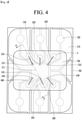
FIG. 4 is a top view of the first surface of the circuit board according to the embodiment and is a view showing both a first circuit pattern and a second circuit pattern. -
FIG. 5 is a view showing a cross-sectional view taken along line A-A' ofFIG. 4 . - Hereinafter, embodiments of the present disclosure will be described in detail with reference to the accompanying drawings. However, the spirit and scope of the present disclosure is not limited to a part of the embodiments described, and may be implemented in various other forms, and within the spirit and scope of the present disclosure, one or more of the elements of the embodiments may be selectively combined and replaced.
- In addition, unless expressly otherwise defined and described, the terms used in the embodiments of the present disclosure (including technical and scientific terms) may be construed the same meaning as commonly understood by one of ordinary skill in the art to which this invention belongs, and the terms such as those defined in commonly used dictionaries may be interpreted as having a meaning that is consistent with their meaning in the context of the relevant art.
- In addition, the terms used in the embodiments of the present disclosure are for describing the embodiments and are not intended to limit the present disclosure. In this specification, the singular forms may also include the plural forms unless specifically stated in the phrase, and may include at least one of all combinations that may be combined in A, B, and C when described in "at least one (or more) of A (and), B, and C".
- Further, in describing the elements of the embodiments of the present disclosure, the terms such as first, second, A, B, (a), and (b) may be used. These terms are only used to distinguish the elements from other elements, and the terms are not limited to the essence, order, or order of the elements.
- In addition, when an element is described as being "connected", "coupled", or "connected" to another element, it may include not only when the element is directly "connected" to, "coupled" to, or "connected" to other elements, but also when the element is "connected", "coupled", or "connected" by another element between the element and other elements.
- Further, when described as being formed or disposed "on (over)" or "under (below)" of each element, the "on (over)" or "under (below)" may include not only when two elements are directly connected to each other, but also when one or more other elements are formed or disposed between two elements.
- Furthermore, when expressed as "on (over)" or "under (below)", it may include not only the upper direction but also the lower direction based on one element.
- Hereinafter, a circuit board according to an embodiment and a smart card for fingerprint recognition including the same will be described with reference to
FIG. 1 . -
FIG. 1 is a view showing a top view of the smart card for fingerprint recognition according to the embodiment. - Referring to
FIG. 1 , a fingerprint recognitionsmart card 1000 may include acard body 1100, acircuit board 1200 accommodated in thecard body 1100, achip 1300, a micro controller unit (MCU) 1400, aconnection circuit pattern 1350 electrically connecting thechip 1300 and themicro controller unit 1400, afingerprint sensor 1500, anantenna 1600, and abattery 1700. - The
circuit board 1200 may be accommodated in thecard body 1100. In detail, an opening OA for accommodating thecircuit board 1200 is formed in the card body 2000, and thecircuit board 1200 may be inserted and adhered to the opening OA. - Accordingly, any one of one surface and the other surface of the
circuit board 1200 may be exposed to the outside of the smart card for fingerprint recognition. - The smart card for fingerprint recognition may include the
fingerprint sensor 1500. Thefingerprint sensor 1500 may recognize a user's fingerprint and match fingerprint information stored in thechip 1300. - That is, one or more predetermined pieces of user's fingerprint information are stored in the
chip 1300, and the fingerprint recognized through thefingerprint sensor 1500 and the fingerprint information stored in thechip 1300 may be matched to compare with each other. - For example, when a user's finger is in contact with the
fingerprint sensor 1500, power is supplied from thebattery 1700 to themicro controller unit 1400, and thefingerprint sensor 1500 supplied with the power by themicro controller unit 1400 may be driven. - Subsequently, the
micro controller unit 1400 may receive the fingerprint information recognized through thefingerprint sensor 1500, and an authentication process of the recognized fingerprint information may be performed. - Subsequently, when the recognized fingerprint information and the fingerprint information stored in the
chip 1300 match, thecircuit board 1200 that is connected to thechip 1300 to serve as a contact pad may be activated, and a function of the smart card for fingerprint recognition may also be activated. - On the other hand, when the recognized fingerprint information and the fingerprint information stored in the
chip 1300 do not match, thecircuit board 1200 connected to thechip 1300 may be deactivated, and the function of the smart card for fingerprint recognition may be also deactivated. - In addition, the smart card for fingerprint recognition may include the
antenna 1600. Accordingly, the smart card for fingerprint recognition may operate as a contactless card. That is, even in a non-contact state with the card reader, information may be wirelessly transmitted and received to and from a server through the antenna of the smart card for fingerprint recognition. - However, the embodiment is not limited thereto, the smart card for fingerprint recognition does not include the
antenna 1600, and the smart card for fingerprint recognition may operate as a contact card. That is, the smart card for fingerprint recognition is inserted into the card reader and may transmit and receive information to and from the server due to contact with the circuit board. - Meanwhile, in order to drive the smart card for fingerprint recognition according to the fingerprint recognition as described above, the
circuit board 1200, thechip 1300, and thefingerprint sensor 1500 should be electrically connected to each other. - In particular, in the case of the smart card for fingerprint recognition, a lot of information such as fingerprint recognition and fingerprint matching of the
fingerprint sensor 1500 is required, and accordingly, a plurality of circuit patterns connected to thechip 1300 are required, and thus a space for the chip and the circuit pattern is required. Accordingly, it is difficult to directly mount the chip on the circuit board, and thechip 1300 disposed outside thecircuit board 1200 may be connected to thecircuit board 1200. - That is, the
circuit board 1200 includes a contact side and a bonding side and is connected to an external chip through the bonding side, and thecircuit board 1200 may be activated or deactivated through the information received from thefingerprint sensor 1500 and thechip 1300. - Meanwhile, the
circuit board 1200 includes asubstrate 100, and circuit patterns are respectively disposed on one surface and the other surface of thesubstrate 100. Electricity should be conducted on the circuit patterns disposed on one surface and the other surface of the substrate in order to operate the circuit board. - In this case, there is a problem that process efficiency is deteriorated due to a longer process time for conducting electricity the circuit patterns.
- The circuit board according to the embodiment is intended to improve the process efficiency by easily connecting the circuit patterns of the bonding side and the contact side as described above.
-
FIGS. 2 to 5 are views for describing a circuit board according to an embodiment. - Referring to
FIGS. 2 to 5 , thecircuit board 1200 may include thesubstrate 100. Thesubstrate 100 may be an insulating substrate. Thesubstrate 100 may include a resin material. Thesubstrate 100 may include onesurface 110 and theother surface 120. The onesurface 110 may be defined as a surface corresponding to the contact side of the circuit pattern described above, and theother surface 120 may be defined as a surface corresponding to the bonding side of the circuit pattern described above. - The
substrate 100 may include prepreg including glass fiber. In detail, thesubstrate 100 may include an epoxy resin and a material in which glass fiber and a silicon-based filler are dispersed in the epoxy resin. - In addition, the
substrate 100 may be rigid or flexible. For example, thesubstrate 100 may include glass or plastic. In detail, thesubstrate 100 may include a chemically tempered/semi-tempered glass, such as soda lime glass, aluminosilicate glass, etc., a tempered or flexible plastic such as polyimide (PI), polyethylene terephthalate (PET), propylene glycol (PPG), polycarbonate (PC), etc., or sapphire. - In addition, the
substrate 100 may include a photoisotropic film. For example, thesubstrate 100 may include cyclic olefin copolymer (COC), cyclic olefin polymer (COP), photoisotropic polycarbonate (PC), photoisotropic polymethyl methacrylate (PMMA), or the like. - Further, the
substrate 100 may be partially bent while having a curved surface. That is, thesubstrate 100 may partially have a plane and may partially be bent while having a curved surface. In detail, an end portion of thesubstrate 100 may be bent while having a curved surface or may be bent or crooked while having a surface with a random curvature. - Furthermore, the
substrate 100 may be a flexible substrate having flexibility. Also, thesubstrate 100 may be a curved or bent substrate. - An
adhesive layer 200 may be disposed on the onesurface 110 and theother surface 120 of thesubstrate 100. Theadhesive layer 200 may be disposed on the entire surface of the one surface and the other surface of thesubstrate 100. In detail, theadhesive layer 200 may be disposed on the entire surface of the one surface and the other surface of the substrate except for a via-formed region. - The
adhesive layer 200 may include a resin material. For example, theadhesive layer 200 may include at least one of an epoxy resin, an acrylic resin, and a polyimide resin. In addition, theadhesive layer 200 may further include additives such as natural rubber, a plasticizer, a hardner, a phosphorus-based flame retardant, and the like in order to impart flexibility to theadhesive layer 200. - Circuit patterns may be respectively disposed on the one
surface 110 and theother surface 120 of thesubstrate 100. - In detail, a
first circuit pattern 310 may be disposed on the onesurface 110, and asecond circuit pattern 320 may be disposed on theother surface 120. - For example, the
first circuit pattern 310 may be a circuit pattern disposed on the contact side of the circuit board, and thesecond circuit pattern 320 may be a circuit pattern disposed on the bonding side of the circuit board. - The
first circuit pattern 310 and thesecond circuit pattern 320 may be disposed on theadhesive layer 200 on thesubstrate 100. - The
first circuit pattern 310 may include a first metal layer 301 and asecond metal layer 302 disposed on the first metal layer 301. In addition, thesecond circuit pattern 320 may include athird metal layer 303 and afourth metal layer 304 disposed on thethird metal layer 303. - The first metal layer 301 and the
third metal layer 303 may include a metal material. In detail, the first metal layer 301 and thethird metal layer 303 may include a metal material having high electrical conductivity. For example, the circuit pattern 300 may include at least one of gold (Au), silver (Ag), platinum (Pt), titanium (Ti), tin (Sn), copper (Cu), and zinc (Zn). Preferably, the first metal layer 301 and thethird metal layer 303 may include copper (Cu). - The
second metal layer 302 and thefourth metal layer 304 may be disposed on the first metal layer 301 and thethird metal layer 303, respectively. - The
second metal layer 302 and thefourth metal layer 304 may be disposed on thefirst circuit pattern 310 and thesecond circuit pattern 320 to protect thefirst circuit pattern 310 and thesecond circuit pattern 320. - In detail, the
second metal layer 302 and thefourth metal layer 304 may include nickel-gold (Ni-Au) or nickel-lead (Ni-Pd), but the embodiment is not limited thereto. Thesecond metal layer 302 and thefourth metal layer 304 may implement various colors depending on the type of material to give a color to the contact side of the smart IC module and prevent corrosion of the circuit pattern. - Referring to
FIG. 2 , thefirst circuit pattern 310 disposed on one surface of thesubstrate 100 may include a plurality of circuit patterns. In detail, thefirst circuit pattern 310 may include the plurality of circuit patterns spaced apart from each other. - Referring to
FIG. 2 , thefirst circuit pattern 310 may include a firstcircuit pattern portion 311, a secondcircuit pattern portion 312, a thirdcircuit pattern portion 313, a fourthcircuit pattern portion 314, a fifthcircuit pattern portion 315, and a sixthcircuit pattern portion 316. -
FIG. 2 illustrates the firstcircuit pattern portion 311, the secondcircuit pattern portion 312, the thirdcircuit pattern portion 313, the fourthcircuit pattern portion 314, the fifthcircuit pattern portion 315, and the sixthcircuit pattern portion 316, but the embodiment is not limited thereto, and thefirst circuit pattern 310 may include less than six or more than six circuit pattern portions. - The first
circuit pattern portion 311, the secondcircuit pattern portion 312, the thirdcircuit pattern portion 313, the fourthcircuit pattern portion 314, the fifthcircuit pattern portion 315, and the sixthcircuit pattern portions 316 may be disposed to be spaced apart from each other. - In addition, referring to
FIG. 3 , thesecond circuit pattern 320 may include a seventhcircuit pattern portion 321, an eighthcircuit pattern portion 322, a ninthcircuit pattern portion 323, a tenthcircuit pattern portion 324, an eleventhcircuit pattern portion 325, and a twelfthcircuit pattern portion 326. -
FIG. 3 illustrates the seventhcircuit pattern portion 321, the eighthcircuit pattern portion 322, the ninthcircuit pattern portion 323, the tenthcircuit pattern portion 324, the eleventhcircuit pattern portion 325, and thetwelfth circuit pattern 326, but the embodiment is not limited thereto, and thesecond circuit pattern 320 may include less than six or more than six circuit pattern portions. - The seventh
circuit pattern portion 321, the eighthcircuit pattern portion 322, the ninthcircuit pattern portion 323, the tenthcircuit pattern portion 324, the eleventhcircuit pattern portion 325, and the twelfthcircuit pattern portions 326 may be disposed to be spaced apart from each other. - The seventh
circuit pattern portion 321, the eighthcircuit pattern portion 322, the ninthcircuit pattern portion 323, the tenthcircuit pattern portion 324, the eleventhcircuit pattern portion 325, and the twelfthcircuit pattern portion 326 may be connected to thefirst circuit pattern 310 disposed on one surface of thesubstrate 100. - To this end, a plurality of vias may be formed in regions corresponding to the respective
first circuit patterns 310 on the other surface of thesubstrate 100. - In detail, a plurality of vias passing through the
adhesive layer 200 and thesubstrate 100 may be formed on theother surface 120 of thesubstrate 100. - Accordingly, on the
other surface 120 of thesubstrate 100, a first via V1 may be formed in a region corresponding to the firstcircuit pattern portion 311, a second via V2 may be formed in a region corresponding to the secondcircuit pattern portion 312, a third via V3 may be formed in a region corresponding to the thirdcircuit pattern portion 313, a fourth via V4 may be formed in the a region corresponding to the fourthcircuit pattern portion 314, a fifth via V5 may be formed in a region corresponding to the fifthcircuit pattern portion 315, and a sixth via V6 may be formed in a region corresponding to the sixthcircuit pattern portion 316. - Referring to
FIG. 4 , thefirst circuit pattern 310 and thesecond circuit pattern 320 may be connected to each other through the vias. - In detail, the
first circuit pattern 310 and thesecond circuit pattern 320 may be electrically connected through wire bonding using a wire. That is, the wire connected to thesecond circuit pattern 320 may be connected to the first circuit pattern through the via. - Meanwhile, a
pad portion 500 may be disposed on one surface of thefirst circuit pattern 310 in contact with the wire. Thepad portion 500 may include a material the same as or similar to that of thefourth metal layer 304 described above. For example, thepad portion 500 may include nickel-gold (Ni-Au) or nickel-lead (Ni-Pd), but the embodiment is not limited thereto. - The first
circuit pattern portion 311 and the seventhcircuit pattern portion 321 may be connected to afirst wire 610 through the first via V1, the secondcircuit pattern portion 312 and the eighthcircuit pattern portion 322 may be connected to asecond wire 620 through the second via V2, the thirdcircuit pattern portion 313 and the ninthcircuit pattern portion 323 may be connected to athird wire 630 through the third via V3, the fourthcircuit pattern portion 314 and the tenthcircuit pattern portion 324 may be connected to afourth wire 640 through the fourth via V4, the fifthcircuit pattern portion 315 and the eleventhcircuit pattern portion 325 may be connected to afifth wire 650 through the fifth via V5, and the sixthcircuit pattern portion 316 and the twelfthcircuit pattern portion 326 may be connected to asixth wire 660 through the sixth via V6. - Accordingly, the
first circuit pattern 310 and thesecond circuit pattern 320 may be electrically connected to conduct electricity to each other. - In the related art, a via was formed to conduct electricity between the first circuit pattern and the second circuit pattern, and a via plating layer was formed on the via to connect the first circuit pattern and the second circuit pattern.
- However, a process for forming the plating layer inside the via is added, and a process time is increased due to a process time of forming the plating layer, so that process efficiency of manufacturing the circuit board may be deteriorated.
- However, in the circuit board according to the embodiment, the process of forming the via plating layer is omitted, and the first circuit pattern and the second circuit pattern are wire-bonded through the via to connect the first circuit pattern and the second circuit pattern, and thus, the connection may be facilitated and the manufacturing process efficiency of the circuit board may be improved.
- Meanwhile, referring to
FIG. 4 , one ends of thefirst wire 610, thesecond wire 620, thethird wire 630, thefourth wire 640, thefifth wire 650, and thesixth wire 660 may be all connected to thesecond circuit pattern 320 in a region corresponding to a singlefirst circuit pattern 310. - That is, a first connection region CA1 of the seventh
circuit pattern portion 321 and thefirst wire 610, a second connection region CA2 of the eighthcircuit pattern portion 322 and thesecond wire 620, a third connection region CA3 of the ninthcircuit pattern portion 323 and thethird wire 630, a fourth connection region CA4 of the tenthcircuit pattern portion 324 and thefourth wire 640, a fifth connection region CA5 of the eleventhcircuit pattern portion 325 and thefifth wire 650, and a sixth connection region CA6 of the twelfthcircuit pattern portion 326 and thesixth wire 660 may be disposed at a position overlapping one circuit pattern among a plurality of circuit pattern portions disposed on the onesurface 110 of thesubstrate 100. - For example, referring to
FIG. 4 , the first connection region CA1, the second connection region CA2, the third connection region CA3, the fourth connection region CA4, the fifth connection region CA5, and the sixth connection region CA6 may overlap only the firstcircuit pattern portion 311 of the first circuit patterns disposed on the onesurface 110 of thesubstrate 100 and may not overlap other circuit pattern portions. - Accordingly, when forming a
molding member 700 for protecting the first connection region CA1, the second connection region CA2, the third connection region CA3, the fourth connection region CA4, the fifth connection region CA5, and the sixth connection region CA6, an area of themolding member 700 may be reduced. - That is, the first connection region CA1, the second connection region CA2, the third connection region CA3, the fourth connection region CA4, the fifth connection region CA5, and the sixth connection region CA6 are not dispersed but concentrated in one region, and thus, it is possible to prevent the area of the
molding member 700 from increasing when the connection regions are molded. - The
substrate 100 may be coupled to the card body 2000 on theother surface 120 that is a bonding side. At this time, an adhesive region for adhering to the card body 2000 is formed on theother surface 120 of thesubstrate 100. As the area of themolding member 700 increases, a position of the adhesive region is limited, and an area of the adhesive region may be reduced. - However, in the circuit board according to the embodiment, the area of the adhesive region of the circuit board may be increased by reducing the area of the
molding member 700. - In addition, referring to
FIG. 3 , a distance between the via and thesecond circuit pattern 320 may be smaller than a distance between the vias. In detail, a minimum distance d1 between the via and thesecond circuit pattern 320 may be smaller than a minimum distance d2 between adjacent vias. - Accordingly, when wire bonding the
second circuit pattern 320 and thefirst circuit pattern 310 through the via, a length of the wire may be prevented from increasing, and thefirst circuit pattern 310 and thesecond circuit pattern 320 may be stably wire-bonded by reducing the distance between thesecond circuit pattern 320 and the via. - The circuit board according to the embodiment may conduct electricity with each other by wire bonding the first circuit pattern and the second circuit pattern through the vias.
- Accordingly, a process of forming a via plating layer in order to conduct electricity between the first circuit pattern and the second circuit pattern may be omitted.
- Therefore, it is possible to prevent deterioration of process efficiency due to an increase in process time due to the formation of the via plating layer.
- In addition, in the circuit board according to the embodiment, the connection region between the second circuit pattern and the wire may be all disposed in a region corresponding to one circuit pattern portion among the plurality of first circuit patterns.
- Accordingly, the area of the molding member for molding the connection region may be reduced.
- Therefore, when the circuit board is adhered to the card body, the area of the adhesive region of the circuit board can be increased, thereby facilitating adhesion between the circuit board and the card body and improving adhesion.
- The characteristics, structures and effects described in the embodiments above are included in at least one embodiment but are not limited to one embodiment. Furthermore, the characteristic, structure, and effect illustrated in each embodiment may be combined or modified for other embodiments by a person skilled in the art. Thus, it should be construed that contents related to such a combination and such a modification are included in the scope of the present disclosure.
- In addition, embodiments are mostly described above, but the embodiments are merely examples and do not limit the present disclosure, and a person skilled in the art may appreciate that several variations and applications not presented above may be made without departing from the essential characteristic of embodiments. For example, each component specifically represented in the embodiments may be varied. In addition, it should be construed that differences related to such a variation and such an application are included in the scope of the present disclosure defined in the following claims.
Claims (15)
- A circuit board comprising:a substrate including one surface and the other surface;a first circuit pattern disposed on the one surface; anda second circuit pattern disposed on the other surface,wherein at least one via is formed in the substrate, andthe first circuit pattern and the second circuit pattern are wire-bonded through the via to conduct electricity.
- The circuit board of claim 1, wherein the first circuit pattern includes a plurality of circuit pattern portions spaced apart from each other,the second circuit pattern includes a plurality of circuit pattern portions spaced apart from each other, andconnection regions of a plurality of wires connected to the plurality of second circuit patterns are disposed in a region corresponding to one circuit pattern portion of the plurality of first circuit patterns.
- The circuit board of claim 1, wherein a minimum distance between the second circuit pattern and the via is smaller than a minimum distance between adjacent vias.
- The circuit board of claim 1, wherein the first circuit pattern or the second circuit pattern is electrically connected to a fingerprint sensor and a chip.
- The circuit board of claim 1, wherein the one surface is a contact side, and
the other surface is a bonding side connected to an external chip. - The circuit board of claim 1, further comprising
an adhesive layer disposed between the substrate and the first circuit pattern and between the substrate and the second circuit pattern. - The circuit board of claim 1, wherein a pad portion is disposed on one surface of the first circuit pattern in contact with the wire.
- The circuit board of claim 1, wherein the first circuit pattern includes a first metal layer and a second metal layer on the first metal layer,the second circuit pattern includes a third metal layer and a fourth metal layer on the third metal layer,the first metal layer and the third metal layer include at least one of gold (Au), silver (Ag), platinum (Pt), titanium (Ti), tin (Sn), copper (Cu), and zinc (Zn), andthe second metal layer and the fourth metal layer include nickel-gold (Ni-Au) or nickel-lead (Ni-Pd).
- The circuit board of claim 1, wherein the first circuit pattern includes a first circuit pattern portion, a second circuit pattern portion, a third circuit pattern portion, a fourth circuit pattern portion, a fifth circuit pattern portion, and a sixth circuit pattern portion that are disposed to be spaced apart from each other, and
the second circuit pattern includes a seventh circuit pattern portion, an eighth circuit pattern portion, a ninth circuit pattern portion, a tenth circuit pattern portion, an eleventh circuit pattern portion, and a twelfth circuit pattern portion that are disposed to be spaced apart from each other. - The circuit board of claim 9, wherein the seventh circuit pattern portion, the eighth circuit pattern portion, the ninth circuit pattern portion, the tenth circuit pattern portion, the eleventh circuit pattern portion, and the twelfth circuit pattern portion are connected to one among the first circuit pattern portion, the second circuit pattern portion, the third circuit pattern portion, the fourth circuit pattern portion, the fifth circuit pattern portion, and the sixth circuit pattern portion.
- The circuit board of claim 9, wherein the seventh circuit pattern portion, the eighth circuit pattern portion, the ninth circuit pattern portion, the tenth circuit pattern portion, the eleventh circuit pattern portion, and the twelfth circuit pattern portion are connected only to the first circuit pattern portion.
- The circuit board of claim 10, wherein the via includes a first via formed in a region corresponding to the seventh circuit pattern portion, a second via formed in a region corresponding to the eighth circuit pattern portion, a third via formed in a region corresponding to the third circuit pattern portion., a fourth via formed in a region corresponding to the fourth circuit pattern portion, a fifth via formed in a region corresponding to the fifth circuit pattern portion, and a sixth via formed in a region corresponding to the sixth circuit pattern portion.
- The circuit board of claim 12, wherein the first circuit pattern portion and the seventh circuit pattern portion are connected to a first wire through the first via,the second circuit pattern portion and the eighth circuit pattern portion are connected to a second wire through the second via,the third circuit pattern portion and the ninth circuit pattern portion are connected to the third wire through the third via,the fourth circuit pattern portion and the tenth circuit pattern portion are connected to a fourth wire through the fourth via,the fifth circuit pattern portion and the eleventh circuit pattern portion are connected to a fifth wire through the fifth via, andthe sixth circuit pattern portion and the twelfth circuit pattern portion are connected to a sixth wire through the sixth via.
- The circuit board of claim 13, further comprising
a molding member disposed on a first connection region between the seventh circuit pattern portion and the first wire, a second connection region between the eighth circuit pattern portion and the second wire, a third connection region between the ninth circuit pattern portion and the third wire, a fourth connection region between the tenth circuit pattern portion and the fourth wire, a fifth connection region between the eleventh circuit pattern portion and the fifth wire, and a sixth connection region between the twelfth circuit pattern portion and the sixth wire. - A smart card for fingerprint recognition comprising:a card body including an opening; anda circuit board of claim 1 accommodated in the opening of the card body,wherein the card body includes:a chip that stores fingerprint information;a micro controller unit;a battery for supplying power to the micro controller unit; anda fingerprint sensor supplied with the power by the micro controller unit,.
Applications Claiming Priority (1)
| Application Number | Priority Date | Filing Date | Title |
|---|---|---|---|
| KR1020200113646A KR102886403B1 (en) | 2020-09-07 | 2020-09-07 | Circuit board and fingerprint recognition smart card including the same |
Publications (1)
| Publication Number | Publication Date |
|---|---|
| EP3972394A1 true EP3972394A1 (en) | 2022-03-23 |
Family
ID=77519028
Family Applications (1)
| Application Number | Title | Priority Date | Filing Date |
|---|---|---|---|
| EP21193299.1A Pending EP3972394A1 (en) | 2020-09-07 | 2021-08-26 | Circuit board and smart card for fingerprint recognition including the same |
Country Status (4)
| Country | Link |
|---|---|
| US (1) | US11900720B2 (en) |
| EP (1) | EP3972394A1 (en) |
| KR (1) | KR102886403B1 (en) |
| CN (1) | CN114154607B (en) |
Families Citing this family (3)
| Publication number | Priority date | Publication date | Assignee | Title |
|---|---|---|---|---|
| JP7614788B2 (en) * | 2020-11-02 | 2025-01-16 | 株式会社東芝 | IC card, portable electronic device and issuing device |
| US20240161534A1 (en) * | 2021-03-23 | 2024-05-16 | Fingerprint Cards Anacatum Ip Ab | Fingerprint sensor module and method for manufacturing a fingerprint sensor module |
| KR20250034713A (en) * | 2023-09-04 | 2025-03-11 | 엘지이노텍 주식회사 | Smart ic substrate, smart ic module and ic card including the same |
Citations (3)
| Publication number | Priority date | Publication date | Assignee | Title |
|---|---|---|---|---|
| US20080197479A1 (en) * | 2007-02-21 | 2008-08-21 | Samsung Electronics Co., Ltd. | Semiconductor package, integrated circuit cards incorporating the semiconductor package, and method of manufacturing the same |
| EP3059698A1 (en) * | 2015-02-20 | 2016-08-24 | Gemalto Sa | Method for manufacturing a single-surface electronic module including interconnection areas |
| US20190392283A1 (en) * | 2014-03-08 | 2019-12-26 | David Finn | Rfid transponder chip modules, elements thereof, and methods |
Family Cites Families (13)
| Publication number | Priority date | Publication date | Assignee | Title |
|---|---|---|---|---|
| JP6090006B2 (en) * | 2013-06-25 | 2017-03-08 | 凸版印刷株式会社 | IC module, dual IC card and IC module manufacturing method |
| CN103886299B (en) | 2014-03-27 | 2019-04-05 | 成都费恩格尔微电子技术有限公司 | Packaging structure of capacitive fingerprint sensor |
| KR101783717B1 (en) * | 2014-07-14 | 2017-10-10 | 브릴리언츠 주식회사 | Multi magnetic card and method for manufacturing magnetic cell |
| CN104766053B (en) | 2015-03-26 | 2018-10-30 | 业成光电(深圳)有限公司 | Fingerprint identification device and its manufacturing method |
| KR101730138B1 (en) * | 2015-12-16 | 2017-04-25 | 주식회사 라이온시큐리티 | Smart card integrated with thermoelement and fingerprint verification chip as laminated structure |
| US9792516B2 (en) | 2016-01-26 | 2017-10-17 | Next Biometrics Group Asa | Flexible card with fingerprint sensor |
| KR101947734B1 (en) | 2017-03-21 | 2019-02-13 | 시그네틱스 주식회사 | Fingerprint recognition sensor package |
| KR102438206B1 (en) | 2017-12-22 | 2022-08-31 | 엘지이노텍 주식회사 | Fingerprint recognition module and electronic device including same |
| CN108021288B (en) | 2017-12-29 | 2020-07-31 | 昆山国显光电有限公司 | Touch panel, manufacturing method thereof and display device |
| CN108089757B (en) * | 2017-12-29 | 2020-03-27 | 云谷(固安)科技有限公司 | Touch panel and touch display device |
| CN110275371A (en) * | 2018-03-18 | 2019-09-24 | 宁波舜宇光电信息有限公司 | Projection arrangement and its manufacturing method and depth information device |
| CN208092769U (en) | 2018-04-16 | 2018-11-13 | 江西立茂科技有限公司 | A kind of fingerprint recognition structure applied to smart card |
| TWI694365B (en) * | 2019-01-16 | 2020-05-21 | 友達光電股份有限公司 | Touch display panel |
-
2020
- 2020-09-07 KR KR1020200113646A patent/KR102886403B1/en active Active
-
2021
- 2021-08-26 EP EP21193299.1A patent/EP3972394A1/en active Pending
- 2021-08-31 US US17/446,541 patent/US11900720B2/en active Active
- 2021-09-06 CN CN202111037931.5A patent/CN114154607B/en active Active
Patent Citations (3)
| Publication number | Priority date | Publication date | Assignee | Title |
|---|---|---|---|---|
| US20080197479A1 (en) * | 2007-02-21 | 2008-08-21 | Samsung Electronics Co., Ltd. | Semiconductor package, integrated circuit cards incorporating the semiconductor package, and method of manufacturing the same |
| US20190392283A1 (en) * | 2014-03-08 | 2019-12-26 | David Finn | Rfid transponder chip modules, elements thereof, and methods |
| EP3059698A1 (en) * | 2015-02-20 | 2016-08-24 | Gemalto Sa | Method for manufacturing a single-surface electronic module including interconnection areas |
Also Published As
| Publication number | Publication date |
|---|---|
| CN114154607A (en) | 2022-03-08 |
| KR102886403B1 (en) | 2025-11-17 |
| US20220078906A1 (en) | 2022-03-10 |
| CN114154607B (en) | 2023-10-27 |
| US11900720B2 (en) | 2024-02-13 |
| KR20220032181A (en) | 2022-03-15 |
Similar Documents
| Publication | Publication Date | Title |
|---|---|---|
| CN114158179B (en) | Intelligent IC substrate, intelligent IC module and IC card comprising same | |
| US11900720B2 (en) | Circuit board and smart card for fingerprint recognition including the same | |
| CN105302361A (en) | Fingerprint sensor and touch device including the same | |
| EP4456677A1 (en) | Smart ic substrate, smart ic module, and ic card comprising same | |
| WO2022157330A1 (en) | Electronic module with indication device | |
| KR20230114877A (en) | Smart ic substrate, smart ic module and ic card including the same | |
| KR102958325B1 (en) | Smart ic substrate module and smart ic substrate | |
| CN121773426A (en) | Intelligent IC substrate, intelligent IC module and IC card comprising intelligent IC module | |
| KR20250014590A (en) | Smart ic substrate, smart ic module and ic card including the same | |
| KR20240168789A (en) | Smart ic substrate, smart ic module and ic card including the same | |
| KR20240124719A (en) | Smart ic substrate, smart ic module and ic card including the same | |
| KR20250066962A (en) | Smart ic substrate, smart ic module and ic card including the same | |
| KR20230116165A (en) | Smart ic substrate module and smart ic substrate | |
| CN121753033A (en) | Intelligent IC substrate, intelligent IC module and IC card comprising intelligent IC module | |
| EP4718316A1 (en) | Smart ic substrate, smart ic module, and ic card comprising same | |
| TWI628600B (en) | Electronic apparatus with embedded fingerprint sensing module | |
| CN121175687A (en) | Intelligent IC substrate, intelligent IC module and IC card comprising intelligent IC module | |
| KR20260010807A (en) | Smart ic substrate, smart ic module and ic card including the same | |
| KR20190091985A (en) | Loop type antenna and rfid card including the same |
Legal Events
| Date | Code | Title | Description |
|---|---|---|---|
| PUAI | Public reference made under article 153(3) epc to a published international application that has entered the european phase |
Free format text: ORIGINAL CODE: 0009012 |
|
| STAA | Information on the status of an ep patent application or granted ep patent |
Free format text: STATUS: REQUEST FOR EXAMINATION WAS MADE |
|
| 17P | Request for examination filed |
Effective date: 20210826 |
|
| AK | Designated contracting states |
Kind code of ref document: A1 Designated state(s): AL AT BE BG CH CY CZ DE DK EE ES FI FR GB GR HR HU IE IS IT LI LT LU LV MC MK MT NL NO PL PT RO RS SE SI SK SM TR |
|
| RBV | Designated contracting states (corrected) |
Designated state(s): AL AT BE BG CH CY CZ DE DK EE ES FI FR GB GR HR HU IE IS IT LI LT LU LV MC MK MT NL NO PL PT RO RS SE SI SK SM TR |
|
| STAA | Information on the status of an ep patent application or granted ep patent |
Free format text: STATUS: EXAMINATION IS IN PROGRESS |
|
| 17Q | First examination report despatched |
Effective date: 20240410 |