EP3968740A1 - Substrate unit and substrate assembly, and camera module using same - Google Patents
Substrate unit and substrate assembly, and camera module using same Download PDFInfo
- Publication number
- EP3968740A1 EP3968740A1 EP21205655.0A EP21205655A EP3968740A1 EP 3968740 A1 EP3968740 A1 EP 3968740A1 EP 21205655 A EP21205655 A EP 21205655A EP 3968740 A1 EP3968740 A1 EP 3968740A1
- Authority
- EP
- European Patent Office
- Prior art keywords
- substrate
- circuit board
- printed circuit
- recess
- substrate part
- Prior art date
- Legal status (The legal status is an assumption and is not a legal conclusion. Google has not performed a legal analysis and makes no representation as to the accuracy of the status listed.)
- Pending
Links
Images


Classifications
-
- H—ELECTRICITY
- H05—ELECTRIC TECHNIQUES NOT OTHERWISE PROVIDED FOR
- H05K—PRINTED CIRCUITS; CASINGS OR CONSTRUCTIONAL DETAILS OF ELECTRIC APPARATUS; MANUFACTURE OF ASSEMBLAGES OF ELECTRICAL COMPONENTS
- H05K1/00—Printed circuits
- H05K1/02—Details
- H05K1/14—Structural association of two or more printed circuits
- H05K1/145—Arrangements wherein electric components are disposed between and simultaneously connected to two planar printed circuit boards, e.g. Cordwood modules
-
- H—ELECTRICITY
- H05—ELECTRIC TECHNIQUES NOT OTHERWISE PROVIDED FOR
- H05K—PRINTED CIRCUITS; CASINGS OR CONSTRUCTIONAL DETAILS OF ELECTRIC APPARATUS; MANUFACTURE OF ASSEMBLAGES OF ELECTRICAL COMPONENTS
- H05K3/00—Apparatus or processes for manufacturing printed circuits
- H05K3/36—Assembling printed circuits with other printed circuits
- H05K3/361—Assembling flexible printed circuits with other printed circuits
- H05K3/365—Assembling flexible printed circuits with other printed circuits by abutting, i.e. without alloying process
-
- H—ELECTRICITY
- H04—ELECTRIC COMMUNICATION TECHNIQUE
- H04N—PICTORIAL COMMUNICATION, e.g. TELEVISION
- H04N23/00—Cameras or camera modules comprising electronic image sensors; Control thereof
- H04N23/50—Constructional details
-
- H—ELECTRICITY
- H04—ELECTRIC COMMUNICATION TECHNIQUE
- H04N—PICTORIAL COMMUNICATION, e.g. TELEVISION
- H04N23/00—Cameras or camera modules comprising electronic image sensors; Control thereof
- H04N23/50—Constructional details
- H04N23/54—Mounting of pick-up tubes, electronic image sensors, deviation or focusing coils
-
- H—ELECTRICITY
- H04—ELECTRIC COMMUNICATION TECHNIQUE
- H04N—PICTORIAL COMMUNICATION, e.g. TELEVISION
- H04N23/00—Cameras or camera modules comprising electronic image sensors; Control thereof
- H04N23/50—Constructional details
- H04N23/55—Optical parts specially adapted for electronic image sensors; Mounting thereof
-
- H—ELECTRICITY
- H04—ELECTRIC COMMUNICATION TECHNIQUE
- H04N—PICTORIAL COMMUNICATION, e.g. TELEVISION
- H04N23/00—Cameras or camera modules comprising electronic image sensors; Control thereof
- H04N23/57—Mechanical or electrical details of cameras or camera modules specially adapted for being embedded in other devices
-
- H—ELECTRICITY
- H05—ELECTRIC TECHNIQUES NOT OTHERWISE PROVIDED FOR
- H05K—PRINTED CIRCUITS; CASINGS OR CONSTRUCTIONAL DETAILS OF ELECTRIC APPARATUS; MANUFACTURE OF ASSEMBLAGES OF ELECTRICAL COMPONENTS
- H05K1/00—Printed circuits
- H05K1/02—Details
-
- H—ELECTRICITY
- H05—ELECTRIC TECHNIQUES NOT OTHERWISE PROVIDED FOR
- H05K—PRINTED CIRCUITS; CASINGS OR CONSTRUCTIONAL DETAILS OF ELECTRIC APPARATUS; MANUFACTURE OF ASSEMBLAGES OF ELECTRICAL COMPONENTS
- H05K1/00—Printed circuits
- H05K1/02—Details
- H05K1/0277—Bendability or stretchability details
- H05K1/028—Bending or folding regions of flexible printed circuits
- H05K1/0281—Reinforcement details thereof
-
- H—ELECTRICITY
- H05—ELECTRIC TECHNIQUES NOT OTHERWISE PROVIDED FOR
- H05K—PRINTED CIRCUITS; CASINGS OR CONSTRUCTIONAL DETAILS OF ELECTRIC APPARATUS; MANUFACTURE OF ASSEMBLAGES OF ELECTRICAL COMPONENTS
- H05K1/00—Printed circuits
- H05K1/02—Details
- H05K1/14—Structural association of two or more printed circuits
-
- H—ELECTRICITY
- H05—ELECTRIC TECHNIQUES NOT OTHERWISE PROVIDED FOR
- H05K—PRINTED CIRCUITS; CASINGS OR CONSTRUCTIONAL DETAILS OF ELECTRIC APPARATUS; MANUFACTURE OF ASSEMBLAGES OF ELECTRICAL COMPONENTS
- H05K1/00—Printed circuits
- H05K1/02—Details
- H05K1/14—Structural association of two or more printed circuits
- H05K1/144—Stacked arrangements of planar printed circuit boards
-
- H—ELECTRICITY
- H05—ELECTRIC TECHNIQUES NOT OTHERWISE PROVIDED FOR
- H05K—PRINTED CIRCUITS; CASINGS OR CONSTRUCTIONAL DETAILS OF ELECTRIC APPARATUS; MANUFACTURE OF ASSEMBLAGES OF ELECTRICAL COMPONENTS
- H05K1/00—Printed circuits
- H05K1/02—Details
- H05K1/14—Structural association of two or more printed circuits
- H05K1/147—Structural association of two or more printed circuits at least one of the printed circuits being bent or folded, e.g. by using a flexible printed circuit
-
- H—ELECTRICITY
- H05—ELECTRIC TECHNIQUES NOT OTHERWISE PROVIDED FOR
- H05K—PRINTED CIRCUITS; CASINGS OR CONSTRUCTIONAL DETAILS OF ELECTRIC APPARATUS; MANUFACTURE OF ASSEMBLAGES OF ELECTRICAL COMPONENTS
- H05K1/00—Printed circuits
- H05K1/02—Details
- H05K1/14—Structural association of two or more printed circuits
- H05K1/148—Arrangements of two or more hingeably connected rigid printed circuit boards, i.e. connected by flexible means
-
- H—ELECTRICITY
- H05—ELECTRIC TECHNIQUES NOT OTHERWISE PROVIDED FOR
- H05K—PRINTED CIRCUITS; CASINGS OR CONSTRUCTIONAL DETAILS OF ELECTRIC APPARATUS; MANUFACTURE OF ASSEMBLAGES OF ELECTRICAL COMPONENTS
- H05K3/00—Apparatus or processes for manufacturing printed circuits
- H05K3/46—Manufacturing multilayer circuits
- H05K3/4688—Composite multilayer circuits, i.e. comprising insulating layers having different properties
- H05K3/4691—Rigid-flexible multilayer circuits comprising rigid and flexible layers, e.g. having in the bending regions only flexible layers
-
- H—ELECTRICITY
- H05—ELECTRIC TECHNIQUES NOT OTHERWISE PROVIDED FOR
- H05K—PRINTED CIRCUITS; CASINGS OR CONSTRUCTIONAL DETAILS OF ELECTRIC APPARATUS; MANUFACTURE OF ASSEMBLAGES OF ELECTRICAL COMPONENTS
- H05K2201/00—Indexing scheme relating to printed circuits covered by H05K1/00
- H05K2201/05—Flexible printed circuits [FPCs]
- H05K2201/056—Folded around rigid support or component
-
- H—ELECTRICITY
- H05—ELECTRIC TECHNIQUES NOT OTHERWISE PROVIDED FOR
- H05K—PRINTED CIRCUITS; CASINGS OR CONSTRUCTIONAL DETAILS OF ELECTRIC APPARATUS; MANUFACTURE OF ASSEMBLAGES OF ELECTRICAL COMPONENTS
- H05K2201/00—Indexing scheme relating to printed circuits covered by H05K1/00
- H05K2201/09—Shape and layout
- H05K2201/09009—Substrate related
- H05K2201/09063—Holes or slots in insulating substrate not used for electrical connections
-
- H—ELECTRICITY
- H05—ELECTRIC TECHNIQUES NOT OTHERWISE PROVIDED FOR
- H05K—PRINTED CIRCUITS; CASINGS OR CONSTRUCTIONAL DETAILS OF ELECTRIC APPARATUS; MANUFACTURE OF ASSEMBLAGES OF ELECTRICAL COMPONENTS
- H05K2201/00—Indexing scheme relating to printed circuits covered by H05K1/00
- H05K2201/09—Shape and layout
- H05K2201/09145—Edge details
-
- H—ELECTRICITY
- H05—ELECTRIC TECHNIQUES NOT OTHERWISE PROVIDED FOR
- H05K—PRINTED CIRCUITS; CASINGS OR CONSTRUCTIONAL DETAILS OF ELECTRIC APPARATUS; MANUFACTURE OF ASSEMBLAGES OF ELECTRICAL COMPONENTS
- H05K2201/00—Indexing scheme relating to printed circuits covered by H05K1/00
- H05K2201/09—Shape and layout
- H05K2201/09145—Edge details
- H05K2201/09163—Slotted edge
-
- H—ELECTRICITY
- H05—ELECTRIC TECHNIQUES NOT OTHERWISE PROVIDED FOR
- H05K—PRINTED CIRCUITS; CASINGS OR CONSTRUCTIONAL DETAILS OF ELECTRIC APPARATUS; MANUFACTURE OF ASSEMBLAGES OF ELECTRICAL COMPONENTS
- H05K2201/00—Indexing scheme relating to printed circuits covered by H05K1/00
- H05K2201/10—Details of components or other objects attached to or integrated in a printed circuit board
- H05K2201/10007—Types of components
- H05K2201/10121—Optical component, e.g. opto-electronic component
-
- H—ELECTRICITY
- H05—ELECTRIC TECHNIQUES NOT OTHERWISE PROVIDED FOR
- H05K—PRINTED CIRCUITS; CASINGS OR CONSTRUCTIONAL DETAILS OF ELECTRIC APPARATUS; MANUFACTURE OF ASSEMBLAGES OF ELECTRICAL COMPONENTS
- H05K2201/00—Indexing scheme relating to printed circuits covered by H05K1/00
- H05K2201/20—Details of printed circuits not provided for in H05K2201/01 - H05K2201/10
- H05K2201/2009—Reinforced areas, e.g. for a specific part of a flexible printed circuit
Definitions
- teachings in accordance with exemplary and non-limiting embodiments of this invention relate generally to a substrate unit and a substrate assembly, and a camera module using the same, and more particularly, to a substrate unit and a substrate assembly used for vehicular cameras, and a camera module using the same.
- the vehicular camera is configured with a lens, an internal circuit and a mechanical structure to support the lens and the internal circuit.
- a plurality of PCBs (Printed Circuit Boards) is overlapped in the course of design, and in order to increase the number of layers to allow overlapping the plurality of PCBs, a rigid flexible PCB (RFPCB) has been disclosed where a plurality of rigid PCBs is connected using flexible PCBs and the flexible PCBs are bent, whereby the plurality of rigid PCBs are arranged to be able to be overlapped.
- the present invention is provide to solve the abovementioned problems/disadvantages, and it is an object of exemplary embodiments of the present invention to provide a substrate unit and a substrate assembly capable of resolving the interference between a rigid PCB and a flexible PCB, and the tearing thereof by providing a reinforcing part in a connection portion of the rigid PCB and the flexible PCB, and a camera module using the same.
- a substrate unit comprising: a first substrate part having rigidity; a second substrate part stacked on one surface of the first substrate part and having flexibility; a third substrate part extending outwardly from the second substrate part and having flexibility; and a reinforcing part which is disposed at a portion where edge portions of the first substrate part and the third substrate part meet, the reinforcing part having a recessed portion which is formed by recessing the first substrate part inwardly so as to prevent interference between the first substrate part and the third substrate part.
- the third substrate part may be disposed at one side of the recessed portion and the other side of the recessed portion may be disposed with a protruding corner part outwardly protruding from the first substrate part, wherein the edge portion where the first substrate part and the third substrate part meet is interposed between a first imaginary extension line extended from the protruding corner part and a second imaginary line parallel with the first imaginary line extended from a bottom surface of the recessed portion.
- At least one portion of the recessed portion may be formed with a radius of curvature of 0.3mm ⁇ 0.5mm.
- a distance between the protruding corner part and the third substrate part may be 0.5mm ⁇ 2.0mm.
- the recessed portion may be recessed at a depth less than 2.0mm from an external side line of the first substrate part.
- the recessed portion may comprise a first lateral part extended from the protruding corner portion by being recessed, a bottom part deeply formed by being connected to the first lateral part, and a rib formed between the first lateral part and the bottom part to have a curvature.
- the recessed portion may further comprise a rib having a curvature from an area where the first substrate part meets the third substrate part to a bottom surface of the recessed portion.
- the reinforcing part may comprise a rib connecting the first substrate part to the third substrate part.
- the rib may have a curvature.
- the second substrate part may have a shape corresponding to that of at least a portion of one surface of the first substrate part.
- a substrate assembly comprising: a plurality of first substrate parts, each having rigidity and disposed in parallel on an imaginary plane surface; a plurality of second substrate parts, each stacked on one surface of each first substrate part and having flexibility; a third substrate part connecting the plurality of second substrate parts and having flexibility; and a reinforcing part disposed at a portion where edge portions of the first substrate part and the third substrate part meet.
- a camera module comprising: a lens part; a lens driving unit driving the lens part; a substrate assembly mounted with an image sensor converting a light received from the lens part to an electric signal, wherein the substrate assembly comprises: a plurality of first substrate parts, each having rigidity and disposed in parallel on an imaginary plane surface; a plurality of second substrate parts, each stacked on one surface of each first substrate part and having flexibility; a third substrate part connecting the plurality of second substrate parts and having flexibility; and a reinforcing part disposed at a portion where edge portions of the first substrate part and the third substrate part meet.
- the present invention can advantageously resolve interference between a rigid PCB and a flexible PCB and a tearing thereof by providing a reinforcing part in a connection portion between the rigid PCB and the flexible PCB.
- first,” “second,” “A”, “B”, (a), (b) and the like, herein do not denote any order, quantity, or importance, but rather are used to distinguish one element from another.
- the terms coupled and/or connected, along with their derivatives may be used.
- connected may be used to indicate that two or more elements are in direct physical and/or electrical contact with each other.
- Coupled may mean that two or more elements are in direct physical and/or electrical contact.
- coupled may also mean that two or more elements may not be in direct contact with each other, but yet may still cooperate and/or interact with each other.
- “coupled”, “joined” and “connected” may mean that two or more elements do not contact each other but are indirectly joined together via another element or intermediate elements.
- FIG. 1 is a perspective view illustrating a camera module according to an exemplary embodiment of the present invention
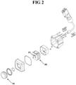
- FIG. 2 is an exploded perspective view illustrating a camera module to an exemplary embodiment of the present invention.
- the camera module may comprise a lens part (10) and a lens driving unit (not shown) and a substrate assembly (20), wherein the substrate assembly (20) may be accommodated into a housing (not shown).
- the lens driving unit can drive the lens part (10).
- the substrate assembly (20) may be mounted with an image sensor (21) converting a light received from the lens part (10) to an electric signal.
- the explanation of substrate unit will replace an explanation of the substrate assembly (20), because the substrate assembly (20) is formed with one substrate part including a plurality of substrate units (described later), i.e., a rigid flexible PCB.
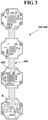
- FIG. 3 is a plane view illustrating a substrate unit or a substrate assembly (20) used for a camera module according to an embodiment of the present invention.
- the substrate unit may comprise a first substrate part (100), a second substrate part (200) and a third substrate part (300), and may further comprise a reinforcing part (400).
- the first substrate part (100) may take a substantially square shape in order to be accommodated into a housing (not shown) and may have rigidity.
- the first substrate part (100) may be preferably formed with a rigid PCB.
- the first substrate part (100) may be formed at a portion of an external shell with a protruding corner part (420).
- An imaginary extension line of the protruding corner part (420) may meet a third substrate part (300) where the protruding corner part (420) is spaced apart from the third substrate part (300).
- the second substrate part (200) may be stacked on one surface of the first substrate part (100).
- the second substrate part (200) may have shape corresponding to that of at least one portion of the one surface of the second substrate part (200).
- the second substrate part (200) may be stacked on a portion of the first substrate part (100) without being stacked on an entire area of the one surface of the first substrate part (100), as long as the second substrate part (200) is electrically connected to the first substrate part (100).
- the second substrate part (200) may have flexibility. That is, the second substrate part (200) is preferably formed with a flexible PCB.
- An edge portion of the first substrate part (100) and an edge portion of the second substrate part (200) may be provided with an avoidance part (500) in order to avoid interference with a screw, where the avoidance part (500) may be connected to the protruding corner part (420).
- the edge portion of the first substrate part (100) and the edge portion of the second substrate part (200) may be formed with a support part (not shown) formed with a through hole (not shown) for passing screw, instead of the avoidance part (500) to allow a substrate unit or a substrate assembly to support the housing, and the edge portion of the first substrate part (100) and the edge portion of the second substrate part (200) may be disposed with the avoidance part (500) and the support part being adjacent to each other.
- the third substrate part (300) may be extended to outside from the second substrate part (200). Furthermore, the third substrate part (300) can electrically connect any one part of the first substrate part (100) to another part of the first substrate part (100). Still furthermore, the third substrate part (300) may be preferably formed with a flexible PCB having flexibility to be extended from the second substrate part (200).
- the reinforcing part (400) may be disposed at a portion where the first substrate part (100) and the third substrate part (300) meet, and the reinforcing part (400) may prevent the third substrate part (300) from being damaged.
- the reinforcing part (400) may comprise a rib (415) connecting the third substrate part (300) with the first substrate part (100), where the rib (415) may have a curvature (see FIGS. 4 to 6 ).
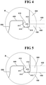
- FIG. 4 is an extracted view of "A" part of FIG. 3 that illustrates the reinforcing part (400).
- the reinforcing part (400) may be disposed at a portion where the first substrate part (100) and the third substrate part (300) meet.
- the first substrate part (100) may comprise a recessed portion (410) that is inwardly recessed in order to prevent the first substrate part (100) and the third substrate part (300) from being mutually interfered.
- the recessed portion (410) may be so formed as to prevent a lateral side of the third substrate part (300) from meeting the first substrate part (100) when the third substrate part (300) is bent. At least one portion of the recessed portion (410) may have a curvature and the at least one portion of the recessed portion may be formed with a radius of curvature of 0.3mm ⁇ 0.5mm.
- the present invention is not limited to a shape for the recessed portion (410).
- One side of the recessed portion (410) may be disposed with the third substrate part (300). That is, the third substrate part (300) may be extended from the second substrate part (200) stacked with on the first substrate part (100), and extended from the second substrate part (200) stacked on another first substrate part (100) to be electrically connected to a plurality of first substrate parts (100). That is, the second substrate part (200) may electrically connect a plurality of first substrate parts (100).
- the recessed portion (410) may comprise a first lateral part (411), a bottom part (413) and a rib (414).
- the other side of the recessed portion (410) may be disposed with a protruding corner portion (420) protruding to outside of the first substrate part (100), and a portion where the first substrate part (100) and the third substrate part (300) meet may be disposed between a first imaginary line (430) extended from the protruding corner portion (420) and a second imaginary line (440) extended from the bottom part (413) of the recessed portion (410) and parallel with a first extended line (430).
- the recessed portion (410) may be such that a distance between the protruding corner portion (420) and the third substrate part (300) is preferably of 0.5mm ⁇ 2.0mm. However, the distance may be variably formed depending on a user's intention. Furthermore, the depth of the recessed portion (410), i.e., a distance between the protruding corner portion (420) and the bottom part (413), may be less than 2.0mm.
- the first lateral part (411) may be connected from the protruding corner part (420) on the first substrate part (100), recessed and extended.
- the bottom part (413) may be connected to the first lateral part (411) to be deeply formed.
- the rib (414) may be disposed at a portion where the first lateral part (411) and the bottom part (413) meet, and may have a curvature.
- the radius of curvature at the rib (414) may be preferably 0.3 mm ⁇ 0.5mm.
- the recessed portion (410) may further comprise a rib (415) having a curvature from a portion where the first substrate part (100) and the third substrate part (300) meet to the bottom part (413) of the recessed portion (410). That is, a rib (415) may be formed that has a curvature from a second lateral part (412) formed at one side of the third substrate part (300) to the bottom part (413), and in this case, the radius of curvature may be preferably 0.3 mm ⁇ 0.5mm.
- the radiuses of curvature of the ribs (414, 415) be same, the radiuses of curvature of the ribs (414, 415) be different, and may be variably formed, depending on the user's intention without being limited to any particular one.
- FIG. 5 is an extracted view of "A" part of FIG. 3 that illustrates a modification of the reinforcing part (400) at FIG. 4 .
- a border between the first substrate part (100) and the third substrate part (300) may match a line imaginarily extended from the bottom part (413) of the recessed portion (410). That is, the protruding corner portion (420) of the recessed portion (410) may be protrudingly formed as much as a depth of the bottom part over the border between the first substrate part (100) and the third substrate part (300). In other words, the border between the first substrate part (100) and the third substrate part (300) may be disposed on an imaginary extension line of the bottom part (413) not interfered with the second lateral part (412).
- FIG. 6 is an extracted view of "A" part of FIG. 3 according to still another exemplary embodiment of FIG. 4 that illustrates a modification of the reinforcing part (400) at FIG. 4 .
- the reinforcing part (400) may not be formed with the recessed portion (410), and the reinforcing part (400) may comprise a rib (415) near the border between the first substrate part (100) and the third substrate part (300). That is, the third substrate part (300) may comprise a rib (415) formed at the edge part with a curvature toward the protruding corner portion (420) of the first substrate part (100). In other words, the border between the first substrate part (100) and the third substrate part (300) may be disposed at an imaginary extension line of the protruding corner portion (420).
- the second substrate part (200) may be understood as having a shape corresponding to that of the first substrate part (100), as being stacked on the first substrate part (100) and extended to the third substrate part (300).
- a substrate assembly (20) may be formed by connecting the substrate units in a plural number according to the hitherto-mentioned exemplary embodiments. That is, in order to implement the camera module according to the exemplary embodiments of the present invention, the camera module may be accommodated therein with the substrate assembly (20) formed with a plurality of substrate units.
- the substrate assembly (20) may comprise a plurality of first substrate parts (100) having rigidity and arranged in parallel on an imaginary plane, a plurality of second substrate parts (200) stacked on each one surface of the plurality of first substrate parts (100) and having flexibility, a third substrate part (300) connecting the plurality of second substrate parts (200) and having flexibility, and a reinforcing part (400) disposed at a portion where the first substrate part (100) and the third substrate part (300) meet and preventing the third substrate part (300) from being damaged.
Landscapes
- Engineering & Computer Science (AREA)
- Microelectronics & Electronic Packaging (AREA)
- Multimedia (AREA)
- Signal Processing (AREA)
- Manufacturing & Machinery (AREA)
- Metallurgy (AREA)
- Studio Devices (AREA)
- Structure Of Printed Boards (AREA)
- Camera Bodies And Camera Details Or Accessories (AREA)
Abstract
Description
- The teachings in accordance with exemplary and non-limiting embodiments of this invention relate generally to a substrate unit and a substrate assembly, and a camera module using the same, and more particularly, to a substrate unit and a substrate assembly used for vehicular cameras, and a camera module using the same.
- Concomitant with increased demands on driver convenience and safety in automobile industries, situations are that new technologies are variously grafted, and particularly, technologies using cameras are briskly applied by being fused with software technologies. Efforts are required to minimize the size of these cameras in order to be mounted on vehicles.
- The vehicular camera is configured with a lens, an internal circuit and a mechanical structure to support the lens and the internal circuit. Thus, in order to reduce the volume the camera, a plurality of PCBs (Printed Circuit Boards) is overlapped in the course of design, and in order to increase the number of layers to allow overlapping the plurality of PCBs, a rigid flexible PCB (RFPCB) has been disclosed where a plurality of rigid PCBs is connected using flexible PCBs and the flexible PCBs are bent, whereby the plurality of rigid PCBs are arranged to be able to be overlapped.
- However, inasmuch as the rigid PCBs and flexible PCBs must be disposed within an allowable space in the aspect of vehicular design, there may be generated interference between the rigid PCBs and the flexible PCBs, as the flexible PCBs are bent, and tearing may be also generated at a connected area between the rigid PCBs and the flexible PCBs.
- The present invention is provide to solve the abovementioned problems/disadvantages, and it is an object of exemplary embodiments of the present invention to provide a substrate unit and a substrate assembly capable of resolving the interference between a rigid PCB and a flexible PCB, and the tearing thereof by providing a reinforcing part in a connection portion of the rigid PCB and the flexible PCB, and a camera module using the same.
- In one general aspect of the present invention, there is provided a substrate unit, comprising: a first substrate part having rigidity; a second substrate part stacked on one surface of the first substrate part and having flexibility; a third substrate part extending outwardly from the second substrate part and having flexibility; and a reinforcing part which is disposed at a portion where edge portions of the first substrate part and the third substrate part meet, the reinforcing part having a recessed portion which is formed by recessing the first substrate part inwardly so as to prevent interference between the first substrate part and the third substrate part.
- Preferably, but not necessarily, the third substrate part may be disposed at one side of the recessed portion and the other side of the recessed portion may be disposed with a protruding corner part outwardly protruding from the first substrate part, wherein the edge portion where the first substrate part and the third substrate part meet is interposed between a first imaginary extension line extended from the protruding corner part and a second imaginary line parallel with the first imaginary line extended from a bottom surface of the recessed portion.
- Preferably, but not necessarily, at least one portion of the recessed portion may be formed with a radius of curvature of 0.3mm ∼ 0.5mm.
- Preferably, but not necessarily, a distance between the protruding corner part and the third substrate part may be 0.5mm ∼ 2.0mm.
- Preferably, but not necessarily, the recessed portion may be recessed at a depth less than 2.0mm from an external side line of the first substrate part.
- Preferably, but not necessarily, the recessed portion may comprise a first lateral part extended from the protruding corner portion by being recessed, a bottom part deeply formed by being connected to the first lateral part, and a rib formed between the first lateral part and the bottom part to have a curvature.
- Preferably, but not necessarily, the recessed portion may further comprise a rib having a curvature from an area where the first substrate part meets the third substrate part to a bottom surface of the recessed portion.
- Preferably, but not necessarily, the reinforcing part may comprise a rib connecting the first substrate part to the third substrate part.
- Preferably, but not necessarily, the rib may have a curvature.
- Preferably, but not necessarily, the second substrate part may have a shape corresponding to that of at least a portion of one surface of the first substrate part.
- In another general aspect of the present invention, there is provided a substrate assembly, comprising: a plurality of first substrate parts, each having rigidity and disposed in parallel on an imaginary plane surface; a plurality of second substrate parts, each stacked on one surface of each first substrate part and having flexibility; a third substrate part connecting the plurality of second substrate parts and having flexibility; and a reinforcing part disposed at a portion where edge portions of the first substrate part and the third substrate part meet.
- In another general aspect of the present invention, there is provided a camera module, comprising: a lens part; a lens driving unit driving the lens part; a substrate assembly mounted with an image sensor converting a light received from the lens part to an electric signal, wherein the substrate assembly comprises: a plurality of first substrate parts, each having rigidity and disposed in parallel on an imaginary plane surface; a plurality of second substrate parts, each stacked on one surface of each first substrate part and having flexibility; a third substrate part connecting the plurality of second substrate parts and having flexibility; and a reinforcing part disposed at a portion where edge portions of the first substrate part and the third substrate part meet.
- Further items regarding the invention are listed below.
- Item 1. A substrate unit, comprising: a first substrate part having rigidity; a second substrate part stacked on one surface of the first substrate part and having flexibility; a third substrate part extending outwardly from the second substrate part and having flexibility; and a reinforcing part which is disposed at a portion where edge portions of the first substrate part and the third substrate part meet, the reinforcing part having a recessed portion which is formed by recessing the first substrate part inwardly so as to prevent interference between the first substrate part and the third substrate part.
- Item 2: The substrate unit of item 1, wherein the third substrate part is disposed at one side of the recessed portion and the other side of the recessed portion is disposed with a protruding corner portion outwardly protruding from the first substrate part, and wherein the edge portion where the first substrate part and the third substrate part meet is interposed between a first imaginary extension line extended from the protruding corner portion and a second imaginary line parallel with the first imaginary line extended from a bottom surface of the recessed portion.
- Item 3: The substrate unit of item 1, wherein at least one portion of the recessed portion is formed with a radius of curvature of 0.3mm ∼ 0.5mm.
- Item 4: The substrate unit of item 2, wherein a distance between the protruding corner portion and the third substrate part is 0.5mm ∼ 2.0mm.
- Item 5: The substrate unit of item 1, wherein the recessed portion is recessed at a depth less than 2.0mm from an external side line of the first substrate part.
- Item 6: The substrate unit of item 2, wherein the recessed portion comprises a first lateral part extended from the protruding corner portion by being recessed, a bottom part deeply formed by being connected to the first lateral part, and a rib formed between the first lateral part and the bottom part to have a curvature.
- Item 7: The substrate unit of item 2, wherein the recessed portion further comprises a rib having a curvature from an area where the first substrate part meets the third substrate part to a bottom surface of the recessed portion.
- Item 8: The substrate unit of item 1, wherein the reinforcing part comprises a rib connecting the first substrate part to the third substrate part.
- Item 9: The substrate unit of item 8, wherein the rib has a curvature.
- Item 10: The substrate unit of item 1, wherein the second substrate part has a shape corresponding to that of at least a portion of one surface of the first substrate part.
- Item 11: A substrate assembly, comprising: a plurality of first substrate parts, each having rigidity and disposed in parallel on an imaginary plane surface; a plurality of second substrate parts, each stacked on one surface of each first substrate part and having flexibility; a third substrate part connecting the plurality of second substrate parts and having flexibility; and a reinforcing part disposed at a portion where edge portions of the first substrate part and the third substrate part meet.
- Item 12: A camera module, comprising: a lens part; a lens driving unit driving the lens part; a substrate assembly mounted with an image sensor converting a light received from the lens part to an electric signal, wherein the substrate assembly comprises: a plurality of first substrate parts, each having rigidity and disposed in parallel on an imaginary plane surface; a plurality of second substrate parts, each stacked on one surface of each first substrate part and having flexibility; a third substrate part connecting the plurality of second substrate parts and having flexibility; and a reinforcing part disposed at a portion where edge portions of the first substrate part and the third substrate part meet.
- The present invention can advantageously resolve interference between a rigid PCB and a flexible PCB and a tearing thereof by providing a reinforcing part in a connection portion between the rigid PCB and the flexible PCB.
-
-
FIG. 1 is a perspective view illustrating a camera module according to an exemplary embodiment of the present invention. -
FIG. 2 is an exploded perspective view illustrating a camera module to an exemplary embodiment of the present invention. -
FIG. 3 is a plane view illustrating a substrate unit and a substrate assembly used for a camera module according to an embodiment of the present invention. -
FIG. 4 is an extracted view of "A" part ofFIG. 3 . -
FIG. 5 is an extracted view of "A" part ofFIG. 3 according to another exemplary embodiment ofFIG. 4 . -
FIG. 6 is an extracted view of "A" part ofFIG. 3 according to still another exemplary embodiment ofFIG. 4 . - Hereinafter, some of exemplary embodiments of the present invention will be described with reference to the accompany drawings.
- Throughout the descriptions, the same reference numerals will be assigned to the same elements in the explanations of the figures, even if shown in different drawings.
- Detailed descriptions of well-known functions, configurations or constructions are omitted for brevity and clarity so as not to obscure the description of the present disclosure with unnecessary detail.
- Furthermore, the terms "first," "second," "A", "B", (a), (b) and the like, herein do not denote any order, quantity, or importance, but rather are used to distinguish one element from another. In the following description and/or claims, the terms coupled and/or connected, along with their derivatives, may be used. In particular embodiments, connected may be used to indicate that two or more elements are in direct physical and/or electrical contact with each other. "Coupled" may mean that two or more elements are in direct physical and/or electrical contact. However, coupled may also mean that two or more elements may not be in direct contact with each other, but yet may still cooperate and/or interact with each other. For example, "coupled", "joined" and "connected" may mean that two or more elements do not contact each other but are indirectly joined together via another element or intermediate elements.
- Hereinafter, a camera module according to an exemplary embodiments of the present invention will be described with reference to the accompany drawings.
-
FIG. 1 is a perspective view illustrating a camera module according to an exemplary embodiment of the present invention, andFIG. 2 is an exploded perspective view illustrating a camera module to an exemplary embodiment of the present invention. - Referring to
FIGS. 1 and2 , the camera module according to an exemplary embodiment of the present invention may comprise a lens part (10) and a lens driving unit (not shown) and a substrate assembly (20), wherein the substrate assembly (20) may be accommodated into a housing (not shown). - Albeit not shown in the drawings, the lens driving unit can drive the lens part (10). Furthermore, the substrate assembly (20) may be mounted with an image sensor (21) converting a light received from the lens part (10) to an electric signal. The explanation of substrate unit will replace an explanation of the substrate assembly (20), because the substrate assembly (20) is formed with one substrate part including a plurality of substrate units (described later), i.e., a rigid flexible PCB.
-
FIG. 3 is a plane view illustrating a substrate unit or a substrate assembly (20) used for a camera module according to an embodiment of the present invention. - Referring to
FIG. 3 , the substrate unit according to an embodiment of the present invention may comprise a first substrate part (100), a second substrate part (200) and a third substrate part (300), and may further comprise a reinforcing part (400). - The first substrate part (100) may take a substantially square shape in order to be accommodated into a housing (not shown) and may have rigidity. In other words, the first substrate part (100) may be preferably formed with a rigid PCB. Furthermore, the first substrate part (100) may be formed at a portion of an external shell with a protruding corner part (420). An imaginary extension line of the protruding corner part (420) may meet a third substrate part (300) where the protruding corner part (420) is spaced apart from the third substrate part (300).
- The second substrate part (200) may be stacked on one surface of the first substrate part (100). The second substrate part (200) may have shape corresponding to that of at least one portion of the one surface of the second substrate part (200). In other words, the second substrate part (200) may be stacked on a portion of the first substrate part (100) without being stacked on an entire area of the one surface of the first substrate part (100), as long as the second substrate part (200) is electrically connected to the first substrate part (100).
- Furthermore, the second substrate part (200) may have flexibility. That is, the second substrate part (200) is preferably formed with a flexible PCB.
- An edge portion of the first substrate part (100) and an edge portion of the second substrate part (200) may be provided with an avoidance part (500) in order to avoid interference with a screw, where the avoidance part (500) may be connected to the protruding corner part (420).
- However, although not illustrated in the drawings, the edge portion of the first substrate part (100) and the edge portion of the second substrate part (200) may be formed with a support part (not shown) formed with a through hole (not shown) for passing screw, instead of the avoidance part (500) to allow a substrate unit or a substrate assembly to support the housing, and the edge portion of the first substrate part (100) and the edge portion of the second substrate part (200) may be disposed with the avoidance part (500) and the support part being adjacent to each other.
- The third substrate part (300) may be extended to outside from the second substrate part (200). Furthermore, the third substrate part (300) can electrically connect any one part of the first substrate part (100) to another part of the first substrate part (100). Still furthermore, the third substrate part (300) may be preferably formed with a flexible PCB having flexibility to be extended from the second substrate part (200).
- The reinforcing part (400) may be disposed at a portion where the first substrate part (100) and the third substrate part (300) meet, and the reinforcing part (400) may prevent the third substrate part (300) from being damaged. As discussed above, the reinforcing part (400) may comprise a rib (415) connecting the third substrate part (300) with the first substrate part (100), where the rib (415) may have a curvature (see
FIGS. 4 to 6 ). -
FIG. 4 is an extracted view of "A" part ofFIG. 3 that illustrates the reinforcing part (400). The reinforcing part (400) may be disposed at a portion where the first substrate part (100) and the third substrate part (300) meet. Furthermore, the first substrate part (100) may comprise a recessed portion (410) that is inwardly recessed in order to prevent the first substrate part (100) and the third substrate part (300) from being mutually interfered. - The recessed portion (410) may be so formed as to prevent a lateral side of the third substrate part (300) from meeting the first substrate part (100) when the third substrate part (300) is bent. At least one portion of the recessed portion (410) may have a curvature and the at least one portion of the recessed portion may be formed with a radius of curvature of 0.3mm ∼0.5mm. The present invention is not limited to a shape for the recessed portion (410).
- One side of the recessed portion (410) may be disposed with the third substrate part (300). That is, the third substrate part (300) may be extended from the second substrate part (200) stacked with on the first substrate part (100), and extended from the second substrate part (200) stacked on another first substrate part (100) to be electrically connected to a plurality of first substrate parts (100). That is, the second substrate part (200) may electrically connect a plurality of first substrate parts (100). The recessed portion (410) may comprise a first lateral part (411), a bottom part (413) and a rib (414).
- The other side of the recessed portion (410) may be disposed with a protruding corner portion (420) protruding to outside of the first substrate part (100), and a portion where the first substrate part (100) and the third substrate part (300) meet may be disposed between a first imaginary line (430) extended from the protruding corner portion (420) and a second imaginary line (440) extended from the bottom part (413) of the recessed portion (410) and parallel with a first extended line (430).
- The recessed portion (410) may be such that a distance between the protruding corner portion (420) and the third substrate part (300) is preferably of 0.5mm ∼2.0mm. However, the distance may be variably formed depending on a user's intention. Furthermore, the depth of the recessed portion (410), i.e., a distance between the protruding corner portion (420) and the bottom part (413), may be less than 2.0mm.
- The first lateral part (411) may be connected from the protruding corner part (420) on the first substrate part (100), recessed and extended. The bottom part (413) may be connected to the first lateral part (411) to be deeply formed. The rib (414) may be disposed at a portion where the first lateral part (411) and the bottom part (413) meet, and may have a curvature. The radius of curvature at the rib (414) may be preferably 0.3 mm ∼ 0.5mm.
- The recessed portion (410) may further comprise a rib (415) having a curvature from a portion where the first substrate part (100) and the third substrate part (300) meet to the bottom part (413) of the recessed portion (410). That is, a rib (415) may be formed that has a curvature from a second lateral part (412) formed at one side of the third substrate part (300) to the bottom part (413), and in this case, the radius of curvature may be preferably 0.3 mm ∼ 0.5mm.
- When the radius of curvature of the rib (414, 415) at the recessed portion (410) is formed to be less than 0.3mm, interference between the first substrate part (100) and the third substrate part (300) may be reduced, but tearing may be generated, and when the radius of curvature of the rib (414, 415) at the recessed portion (410) is formed to be greater than 0.5mm, the tearing of the first substrate part (100) and the third substrate part (300) may be reduced but the interference may be generated. Although it is preferable that the radiuses of curvature of the ribs (414, 415) be same, the radiuses of curvature of the ribs (414, 415) be different, and may be variably formed, depending on the user's intention without being limited to any particular one.
-
FIG. 5 is an extracted view of "A" part ofFIG. 3 that illustrates a modification of the reinforcing part (400) atFIG. 4 . - Referring to
FIG. 5 , a border between the first substrate part (100) and the third substrate part (300) may match a line imaginarily extended from the bottom part (413) of the recessed portion (410). That is, the protruding corner portion (420) of the recessed portion (410) may be protrudingly formed as much as a depth of the bottom part over the border between the first substrate part (100) and the third substrate part (300). In other words, the border between the first substrate part (100) and the third substrate part (300) may be disposed on an imaginary extension line of the bottom part (413) not interfered with the second lateral part (412). -
FIG. 6 is an extracted view of "A" part ofFIG. 3 according to still another exemplary embodiment ofFIG. 4 that illustrates a modification of the reinforcing part (400) atFIG. 4 . - Referring to
FIG. 6 , the reinforcing part (400) may not be formed with the recessed portion (410), and the reinforcing part (400) may comprise a rib (415) near the border between the first substrate part (100) and the third substrate part (300). That is, the third substrate part (300) may comprise a rib (415) formed at the edge part with a curvature toward the protruding corner portion (420) of the first substrate part (100). In other words, the border between the first substrate part (100) and the third substrate part (300) may be disposed at an imaginary extension line of the protruding corner portion (420). - Now, referring to
FIGS. 4 to 6 , albeit the second substrate part (200) not being illustrated, the second substrate part (200) may be understood as having a shape corresponding to that of the first substrate part (100), as being stacked on the first substrate part (100) and extended to the third substrate part (300). - The exemplary embodiments or modifications discussed above are mere examples, and are not limited to the contents mentioned above, and may have various changes depending on a manufacturers' intentions.
- A substrate assembly (20) may be formed by connecting the substrate units in a plural number according to the hitherto-mentioned exemplary embodiments. That is, in order to implement the camera module according to the exemplary embodiments of the present invention, the camera module may be accommodated therein with the substrate assembly (20) formed with a plurality of substrate units.
- In other words, the substrate assembly (20) may comprise a plurality of first substrate parts (100) having rigidity and arranged in parallel on an imaginary plane, a plurality of second substrate parts (200) stacked on each one surface of the plurality of first substrate parts (100) and having flexibility, a third substrate part (300) connecting the plurality of second substrate parts (200) and having flexibility, and a reinforcing part (400) disposed at a portion where the first substrate part (100) and the third substrate part (300) meet and preventing the third substrate part (300) from being damaged.
- Although the abovementioned embodiments are merely exemplary in order to implement a substrate unit, a substrate assembly and a camera module using the same according to the present invention, the embodiments are, however, intended to be illustrative only, and thereby do not limit the scope of protection of the present invention.
- Thereby, it should be appreciated by the skilled in the art that changes, modifications and amendments to the above examples may be made without deviating from the scope of protection of the invention.
Claims (13)
- A substrate unit (20), comprising:a first printed circuit board (100); anda flexible printed circuit board (300) coupled to the first printed circuit board (100),wherein the first printed circuit board (100) comprises a first lateral surface (420), a second lateral surface, and a recess (410) between the first lateral surface (420) and the second lateral surface,wherein a first imaginary line (430) meets the first lateral surface (420) of the first printed circuit board (100),wherein a second imaginary line (440) parallel to the first imaginary line (430) meets a bottom surface (413) of the recess (410) of the first printed circuit board (100),wherein a third imaginary line is disposed between the first imaginary line (430) and the second imaginary line (440), and meets the second lateral surface of the first printed circuit board (100), andwherein the second lateral surface of the first printed circuit board (100) is overlapped with the flexible printed circuit board (300).
- The substrate unit (20) of claim 1, wherein the first printed circuit board (100) is a rigid printed circuit board.
- The substrate unit (20) of claim 1 or 2, wherein the second lateral surface is disposed at a position further inward than is a position of the first lateral surface (420), and
wherein the second lateral surface of the printed circuit board is disposed such that it protrudes more than the bottom surface (413) of the recess (410) does. - The substrate unit (20) of any one claim of claims 1 to 3, wherein the recess (410) comprises a first lateral part (411) connected to the first lateral surface (420) of the first printed circuit board (100) and facing the flexible printed circuit board (300),wherein the recess (410) comprises a first rib (414) connecting the first lateral part (411) of the recess (410) and the bottom surface (413) of the recess (410), andwherein the first rib (414) of the recess (410) is formed in a round shape.
- The substrate unit (20) of claim 4, wherein the recess (410) comprises a second lateral part (412) facing the first lateral part (411) of the recess (410), and a second rib (415) connecting the bottom surface (413) of the recess (410) and the second lateral part (412) of the recess (410), and
wherein the second rib (415) of the recess (410) is formed in a round shape. - The substrate unit (20) of claim 5, wherein a curvature of the first rib (414) is different from a curvature of the second rib (415).
- The substrate unit (20) of any one claim of claims 1 to 6, wherein at least one portion of the recess (410) of the first printed circuit board (100) is formed with a radius of curvature of 0.3 mm - 0.5 mm.
- The substrate unit (20) of any one claim of claims 1 to 7, wherein the recess (410) comprises a first surface connected to the first lateral surface (420) of the first printed circuit board (100), and facing the flexible printed circuit board (300), and
wherein a distance between the first surface of the recess (410) and the flexible printed circuit board (300) is 0.5 mm - 2.0 mm. - The substrate unit (20) of any one claim of claims 1 to 8, wherein the recess (410) comprises a curved surface spaced apart from the flexible printed circuit board (300),wherein the curved surface of the recess (410) of the first printed circuit board (100) has a curvature, andwherein a radius of the curvature of the curved surface is 0.3 mm - 0.5 mm.
- The substrate unit (20) of any one claim of claims 1 to 9, wherein the recess (410) is opened in a direction perpendicular to the third imaginary line.
- The substrate unit (20) of claim any one claim of claims 1 to 10, wherein edge portions of the first printed circuit board (100) comprise avoidance parts recessed inwardly.
- A substrate assembly, comprising a plurality of the substrate unit of any one claim of claims 1 to 11.
- A camera module, comprising:a lens part (10);a lens driving unit driving the lens part (10);a substrate assembly (20) of claim 12 mounted with an image sensor (21) converting a light received from the lens part (10) to an electric signal.
Applications Claiming Priority (3)
| Application Number | Priority Date | Filing Date | Title |
|---|---|---|---|
| KR1020150108006A KR102415361B1 (en) | 2015-07-30 | 2015-07-30 | Printed circuit board unit |
| EP16830823.7A EP3331333B1 (en) | 2015-07-30 | 2016-07-27 | Substrate unit and substrate assembly, and camera module using same |
| PCT/KR2016/008178 WO2017018790A1 (en) | 2015-07-30 | 2016-07-27 | Substrate unit and substrate assembly, and camera module using same |
Related Parent Applications (2)
| Application Number | Title | Priority Date | Filing Date |
|---|---|---|---|
| EP16830823.7A Division EP3331333B1 (en) | 2015-07-30 | 2016-07-27 | Substrate unit and substrate assembly, and camera module using same |
| EP16830823.7A Division-Into EP3331333B1 (en) | 2015-07-30 | 2016-07-27 | Substrate unit and substrate assembly, and camera module using same |
Publications (1)
| Publication Number | Publication Date |
|---|---|
| EP3968740A1 true EP3968740A1 (en) | 2022-03-16 |
Family
ID=57884718
Family Applications (2)
| Application Number | Title | Priority Date | Filing Date |
|---|---|---|---|
| EP16830823.7A Active EP3331333B1 (en) | 2015-07-30 | 2016-07-27 | Substrate unit and substrate assembly, and camera module using same |
| EP21205655.0A Pending EP3968740A1 (en) | 2015-07-30 | 2016-07-27 | Substrate unit and substrate assembly, and camera module using same |
Family Applications Before (1)
| Application Number | Title | Priority Date | Filing Date |
|---|---|---|---|
| EP16830823.7A Active EP3331333B1 (en) | 2015-07-30 | 2016-07-27 | Substrate unit and substrate assembly, and camera module using same |
Country Status (5)
| Country | Link |
|---|---|
| US (7) | US10334743B2 (en) |
| EP (2) | EP3331333B1 (en) |
| KR (4) | KR102415361B1 (en) |
| CN (3) | CN107852814B (en) |
| WO (1) | WO2017018790A1 (en) |
Families Citing this family (11)
| Publication number | Priority date | Publication date | Assignee | Title |
|---|---|---|---|---|
| KR102415361B1 (en) | 2015-07-30 | 2022-07-01 | 엘지이노텍 주식회사 | Printed circuit board unit |
| EP3288248B1 (en) * | 2016-08-25 | 2019-01-23 | Guangdong Oppo Mobile Telecommunications Corp., Ltd | Mobile terminal, housing component, and manufacturing method thereof |
| US11109478B2 (en) * | 2017-11-15 | 2021-08-31 | Steering Solutions Ip Holding Corporation | Semi-flexible ridged printed circuit board assembly |
| US11885955B2 (en) | 2018-11-22 | 2024-01-30 | Ningbo Sunny Opotech Co., Ltd. | Circuit board, circuit board jointed panel, periscope camera module, and application thereof |
| CN109587382B (en) * | 2018-12-18 | 2024-09-27 | 青岛小鸟看看科技有限公司 | Camera module and depth camera |
| CN109831872A (en) * | 2019-03-19 | 2019-05-31 | 北京遥感设备研究所 | It is a kind of can the combination of laterally attached multilayer circuit rigid flex-circuits plate |
| US11172574B2 (en) | 2019-03-22 | 2021-11-09 | Samsung Electro-Mechanics Co., Ltd. | Printed circuit board assembly |
| KR102217402B1 (en) * | 2019-06-07 | 2021-02-19 | 주식회사 디에스전자 | Transmitter receiver module for active phased array radar using Flex-rigid board |
| US11594824B2 (en) | 2019-10-17 | 2023-02-28 | Qualcomm Incorporated | Integrated antenna module |
| KR20220160211A (en) * | 2021-05-27 | 2022-12-06 | 엘지이노텍 주식회사 | Camera actuator and camera device comprising the same |
| JP2025090209A (en) | 2023-12-05 | 2025-06-17 | 京セラドキュメントソリューションズ株式会社 | Inkjet image forming device |
Citations (6)
| Publication number | Priority date | Publication date | Assignee | Title |
|---|---|---|---|---|
| JPH0758424A (en) * | 1993-08-18 | 1995-03-03 | Sharp Corp | Flex rigid printed wiring board |
| US20060141226A1 (en) * | 2004-12-03 | 2006-06-29 | Fuji Photo Film Co., Ltd. | Printed circuit board and camera module |
| US20100188565A1 (en) * | 2009-01-27 | 2010-07-29 | Sony Corporation | Circuit-substrate support structure and image-acquisition device |
| US20110198111A1 (en) * | 2010-02-12 | 2011-08-18 | Ibiden Co., Ltd. | Flex-rigid wiring board and method for manufacturing the same |
| JP2012069971A (en) * | 2010-06-03 | 2012-04-05 | Konica Minolta Opto Inc | Printed wiring board connecting structure, and camera module |
| US20140036218A1 (en) * | 2012-08-06 | 2014-02-06 | Yun-Kai Yu | Camera module and method for making same |
Family Cites Families (26)
| Publication number | Priority date | Publication date | Assignee | Title |
|---|---|---|---|---|
| JPH1138430A (en) * | 1997-07-17 | 1999-02-12 | Hitachi Ltd | Liquid crystal display |
| JP2002109998A (en) * | 2000-07-12 | 2002-04-12 | Agfa Gevaert Nv | Switch with at least one flexible conductive member |
| KR100340285B1 (en) * | 2000-10-24 | 2002-06-15 | 윤종용 | Memory module having series-connected printed circuit boards |
| JP4050972B2 (en) * | 2002-10-16 | 2008-02-20 | 株式会社 日立ディスプレイズ | Display device |
| WO2004095832A1 (en) * | 2003-04-22 | 2004-11-04 | Konica Minolta Opto, Inc. | Imaging device and mobile terminal using this imaging device |
| EP1707103A4 (en) | 2004-01-19 | 2010-12-15 | Olympus Corp | Imaging device for endoscope and capsule type endoscope |
| JP2006173477A (en) * | 2004-12-17 | 2006-06-29 | Fujikura Ltd | Rigid flex multilayer printed wiring board and method for manufacturing the same |
| JP2007067244A (en) * | 2005-08-31 | 2007-03-15 | Sony Corp | Circuit board |
| KR100716788B1 (en) | 2005-10-14 | 2007-05-14 | 삼성전기주식회사 | Substrate for image sensor module and image sensor module using same |
| KR100730062B1 (en) | 2006-03-21 | 2007-06-20 | 삼성전기주식회사 | Camera module with improved noise characteristics |
| JP2007299784A (en) * | 2006-04-27 | 2007-11-15 | Toshiba Corp | Mounting structure and electronic device having mounting structure |
| KR100821043B1 (en) * | 2006-09-22 | 2008-04-08 | 삼성에스디아이 주식회사 | Flexible Printed Circuit Board |
| JP2008112070A (en) * | 2006-10-31 | 2008-05-15 | Sharp Corp | Inter-substrate connection structure, inter-substrate connection method, display device |
| JP2009115942A (en) * | 2007-11-05 | 2009-05-28 | Sharp Corp | Liquid crystal display device |
| JP2009182002A (en) * | 2008-01-29 | 2009-08-13 | Kyocera Corp | Substrate connection structure and electronic device |
| KR101055449B1 (en) | 2009-09-03 | 2011-08-08 | 삼성전기주식회사 | Camera module |
| DE102010028990A1 (en) * | 2010-05-14 | 2011-12-01 | Lenze Automation Gmbh | Printed circuit board composite, has coupling circuit boards passing through corresponding inserted openings and corresponding female connector, where printed circuit boards form planes parallel to each other |
| KR20110127913A (en) * | 2010-05-20 | 2011-11-28 | 삼성전자주식회사 | Camera module |
| US8351579B2 (en) * | 2010-09-22 | 2013-01-08 | Wipro Limited | System and method for securely authenticating and lawfully intercepting data in telecommunication networks using biometrics |
| KR101428842B1 (en) | 2011-11-08 | 2014-08-08 | 엘지이노텍 주식회사 | Camera module for Vehicle |
| KR101343217B1 (en) * | 2012-05-07 | 2013-12-18 | 삼성전기주식회사 | Rigid-flexible printed circuit board and method for manufacturing thereof |
| US9113551B2 (en) * | 2012-07-17 | 2015-08-18 | Google Inc. | Rigid flex circuit board |
| CN203259691U (en) * | 2013-05-07 | 2013-10-30 | 苏州旭创科技有限公司 | Parallel optical transmission-reception assembly for micro serial SCSI broadband high-speed transmission |
| JP5902352B2 (en) * | 2013-06-21 | 2016-04-13 | 富士フイルム株式会社 | Electrical contact device, lens unit, imaging device |
| KR20160103083A (en) * | 2013-12-24 | 2016-08-31 | 폴리에라 코퍼레이션 | Support structures for an attachable, two-dimensional flexible electronic device |
| KR102415361B1 (en) | 2015-07-30 | 2022-07-01 | 엘지이노텍 주식회사 | Printed circuit board unit |
-
2015
- 2015-07-30 KR KR1020150108006A patent/KR102415361B1/en active Active
-
2016
- 2016-07-27 EP EP16830823.7A patent/EP3331333B1/en active Active
- 2016-07-27 CN CN201680044832.0A patent/CN107852814B/en active Active
- 2016-07-27 CN CN202110874104.5A patent/CN113709965B/en active Active
- 2016-07-27 WO PCT/KR2016/008178 patent/WO2017018790A1/en not_active Ceased
- 2016-07-27 CN CN202110874087.5A patent/CN113709964B/en active Active
- 2016-07-27 EP EP21205655.0A patent/EP3968740A1/en active Pending
- 2016-07-27 US US15/748,999 patent/US10334743B2/en active Active
-
2019
- 2019-05-07 US US16/405,446 patent/US10765014B2/en active Active
-
2020
- 2020-07-24 US US16/937,772 patent/US11172582B2/en active Active
-
2021
- 2021-09-09 US US17/447,254 patent/US11582873B2/en active Active
-
2022
- 2022-06-27 KR KR1020220078368A patent/KR102552749B1/en active Active
-
2023
- 2023-01-11 US US18/152,918 patent/US11937382B2/en active Active
- 2023-07-03 KR KR1020230086132A patent/KR102692363B1/en active Active
-
2024
- 2024-02-15 US US18/442,659 patent/US12342475B2/en active Active
- 2024-08-01 KR KR1020240102348A patent/KR20240122710A/en active Pending
-
2025
- 2025-06-23 US US19/246,285 patent/US20250318055A1/en active Pending
Patent Citations (6)
| Publication number | Priority date | Publication date | Assignee | Title |
|---|---|---|---|---|
| JPH0758424A (en) * | 1993-08-18 | 1995-03-03 | Sharp Corp | Flex rigid printed wiring board |
| US20060141226A1 (en) * | 2004-12-03 | 2006-06-29 | Fuji Photo Film Co., Ltd. | Printed circuit board and camera module |
| US20100188565A1 (en) * | 2009-01-27 | 2010-07-29 | Sony Corporation | Circuit-substrate support structure and image-acquisition device |
| US20110198111A1 (en) * | 2010-02-12 | 2011-08-18 | Ibiden Co., Ltd. | Flex-rigid wiring board and method for manufacturing the same |
| JP2012069971A (en) * | 2010-06-03 | 2012-04-05 | Konica Minolta Opto Inc | Printed wiring board connecting structure, and camera module |
| US20140036218A1 (en) * | 2012-08-06 | 2014-02-06 | Yun-Kai Yu | Camera module and method for making same |
Also Published As
| Publication number | Publication date |
|---|---|
| US20210410298A1 (en) | 2021-12-30 |
| US10765014B2 (en) | 2020-09-01 |
| CN113709965A (en) | 2021-11-26 |
| US11582873B2 (en) | 2023-02-14 |
| CN107852814B (en) | 2021-08-24 |
| KR20170014504A (en) | 2017-02-08 |
| CN113709964B (en) | 2023-07-18 |
| US12342475B2 (en) | 2025-06-24 |
| CN113709964A (en) | 2021-11-26 |
| US20200359509A1 (en) | 2020-11-12 |
| EP3331333A1 (en) | 2018-06-06 |
| EP3331333A4 (en) | 2019-04-17 |
| CN113709965B (en) | 2023-07-21 |
| US20180332722A1 (en) | 2018-11-15 |
| US10334743B2 (en) | 2019-06-25 |
| KR102552749B1 (en) | 2023-07-07 |
| KR20230107180A (en) | 2023-07-14 |
| KR102692363B1 (en) | 2024-08-07 |
| EP3331333B1 (en) | 2021-12-22 |
| US20190269022A1 (en) | 2019-08-29 |
| US20240188229A1 (en) | 2024-06-06 |
| US20230171899A1 (en) | 2023-06-01 |
| CN107852814A (en) | 2018-03-27 |
| US20250318055A1 (en) | 2025-10-09 |
| KR102415361B1 (en) | 2022-07-01 |
| US11172582B2 (en) | 2021-11-09 |
| KR20220093308A (en) | 2022-07-05 |
| US11937382B2 (en) | 2024-03-19 |
| KR20240122710A (en) | 2024-08-13 |
| WO2017018790A1 (en) | 2017-02-02 |
Similar Documents
| Publication | Publication Date | Title |
|---|---|---|
| US12342475B2 (en) | Substrate unit and substrate assembly, and camera module using same | |
| JP7698015B2 (en) | Circuit board fixing device for camera module and camera module | |
| US10558108B2 (en) | Camera module | |
| KR20240130674A (en) | Circuit board fixing device and camera module having the same | |
| WO2011082715A1 (en) | A camera for a motor vehicle and a method for manufacturing such a camera |
Legal Events
| Date | Code | Title | Description |
|---|---|---|---|
| PUAI | Public reference made under article 153(3) epc to a published international application that has entered the european phase |
Free format text: ORIGINAL CODE: 0009012 |
|
| STAA | Information on the status of an ep patent application or granted ep patent |
Free format text: STATUS: THE APPLICATION HAS BEEN PUBLISHED |
|
| AC | Divisional application: reference to earlier application |
Ref document number: 3331333 Country of ref document: EP Kind code of ref document: P |
|
| AK | Designated contracting states |
Kind code of ref document: A1 Designated state(s): AL AT BE BG CH CY CZ DE DK EE ES FI FR GB GR HR HU IE IS IT LI LT LU LV MC MK MT NL NO PL PT RO RS SE SI SK SM TR |
|
| STAA | Information on the status of an ep patent application or granted ep patent |
Free format text: STATUS: REQUEST FOR EXAMINATION WAS MADE |
|
| 17P | Request for examination filed |
Effective date: 20220801 |
|
| RBV | Designated contracting states (corrected) |
Designated state(s): AL AT BE BG CH CY CZ DE DK EE ES FI FR GB GR HR HU IE IS IT LI LT LU LV MC MK MT NL NO PL PT RO RS SE SI SK SM TR |
|
| STAA | Information on the status of an ep patent application or granted ep patent |
Free format text: STATUS: EXAMINATION IS IN PROGRESS |