EP3968458B1 - Radiating structure and array antenna - Google Patents
Radiating structure and array antenna Download PDFInfo
- Publication number
- EP3968458B1 EP3968458B1 EP19928598.2A EP19928598A EP3968458B1 EP 3968458 B1 EP3968458 B1 EP 3968458B1 EP 19928598 A EP19928598 A EP 19928598A EP 3968458 B1 EP3968458 B1 EP 3968458B1
- Authority
- EP
- European Patent Office
- Prior art keywords
- radiating
- slot
- sheet
- antenna
- recited
- Prior art date
- Legal status (The legal status is an assumption and is not a legal conclusion. Google has not performed a legal analysis and makes no representation as to the accuracy of the status listed.)
- Active
Links
Images

Classifications
-
- H—ELECTRICITY
- H01—ELECTRIC ELEMENTS
- H01Q—ANTENNAS, i.e. RADIO AERIALS
- H01Q1/00—Details of, or arrangements associated with, antennas
- H01Q1/12—Supports; Mounting means
- H01Q1/22—Supports; Mounting means by structural association with other equipment or articles
- H01Q1/24—Supports; Mounting means by structural association with other equipment or articles with receiving set
- H01Q1/241—Supports; Mounting means by structural association with other equipment or articles with receiving set used in mobile communications, e.g. GSM
- H01Q1/246—Supports; Mounting means by structural association with other equipment or articles with receiving set used in mobile communications, e.g. GSM specially adapted for base stations
-
- H—ELECTRICITY
- H01—ELECTRIC ELEMENTS
- H01Q—ANTENNAS, i.e. RADIO AERIALS
- H01Q1/00—Details of, or arrangements associated with, antennas
- H01Q1/36—Structural form of radiating elements, e.g. cone, spiral, umbrella; Particular materials used therewith
-
- H—ELECTRICITY
- H01—ELECTRIC ELEMENTS
- H01Q—ANTENNAS, i.e. RADIO AERIALS
- H01Q1/00—Details of, or arrangements associated with, antennas
- H01Q1/50—Structural association of antennas with earthing switches, lead-in devices or lightning protectors
-
- H—ELECTRICITY
- H01—ELECTRIC ELEMENTS
- H01Q—ANTENNAS, i.e. RADIO AERIALS
- H01Q1/00—Details of, or arrangements associated with, antennas
- H01Q1/52—Means for reducing coupling between antennas; Means for reducing coupling between an antenna and another structure
-
- H—ELECTRICITY
- H01—ELECTRIC ELEMENTS
- H01Q—ANTENNAS, i.e. RADIO AERIALS
- H01Q1/00—Details of, or arrangements associated with, antennas
- H01Q1/52—Means for reducing coupling between antennas; Means for reducing coupling between an antenna and another structure
- H01Q1/521—Means for reducing coupling between antennas; Means for reducing coupling between an antenna and another structure reducing the coupling between adjacent antennas
- H01Q1/523—Means for reducing coupling between antennas; Means for reducing coupling between an antenna and another structure reducing the coupling between adjacent antennas between antennas of an array
-
- H—ELECTRICITY
- H01—ELECTRIC ELEMENTS
- H01Q—ANTENNAS, i.e. RADIO AERIALS
- H01Q13/00—Waveguide horns or mouths; Slot antennas; Leaky-waveguide antennas; Equivalent structures causing radiation along the transmission path of a guided wave
- H01Q13/10—Resonant slot antennas
-
- H—ELECTRICITY
- H01—ELECTRIC ELEMENTS
- H01Q—ANTENNAS, i.e. RADIO AERIALS
- H01Q15/00—Devices for reflection, refraction, diffraction or polarisation of waves radiated from an antenna, e.g. quasi-optical devices
- H01Q15/24—Polarising devices; Polarisation filters
-
- H—ELECTRICITY
- H01—ELECTRIC ELEMENTS
- H01Q—ANTENNAS, i.e. RADIO AERIALS
- H01Q19/00—Combinations of primary active antenna elements and units with secondary devices, e.g. with quasi-optical devices, for giving the antenna a desired directional characteristic
- H01Q19/10—Combinations of primary active antenna elements and units with secondary devices, e.g. with quasi-optical devices, for giving the antenna a desired directional characteristic using reflecting surfaces
- H01Q19/104—Combinations of primary active antenna elements and units with secondary devices, e.g. with quasi-optical devices, for giving the antenna a desired directional characteristic using reflecting surfaces using a substantially flat reflector for deflecting the radiated beam, e.g. periscopic antennas
-
- H—ELECTRICITY
- H01—ELECTRIC ELEMENTS
- H01Q—ANTENNAS, i.e. RADIO AERIALS
- H01Q21/00—Antenna arrays or systems
- H01Q21/0006—Particular feeding systems
-
- H—ELECTRICITY
- H01—ELECTRIC ELEMENTS
- H01Q—ANTENNAS, i.e. RADIO AERIALS
- H01Q21/00—Antenna arrays or systems
- H01Q21/06—Arrays of individually energised antenna units similarly polarised and spaced apart
- H01Q21/061—Two dimensional planar arrays
-
- H—ELECTRICITY
- H01—ELECTRIC ELEMENTS
- H01Q—ANTENNAS, i.e. RADIO AERIALS
- H01Q21/00—Antenna arrays or systems
- H01Q21/24—Combinations of antenna units polarised in different directions for transmitting or receiving circularly and elliptically polarised waves or waves linearly polarised in any direction
- H01Q21/26—Turnstile or like antennas comprising arrangements of three or more elongated elements disposed radially and symmetrically in a horizontal plane about a common centre
-
- H—ELECTRICITY
- H01—ELECTRIC ELEMENTS
- H01Q—ANTENNAS, i.e. RADIO AERIALS
- H01Q9/00—Electrically-short antennas having dimensions not more than twice the operating wavelength and consisting of conductive active radiating elements
- H01Q9/04—Resonant antennas
- H01Q9/16—Resonant antennas with feed intermediate between the extremities of the antenna, e.g. centre-fed dipole
- H01Q9/26—Resonant antennas with feed intermediate between the extremities of the antenna, e.g. centre-fed dipole with folded element or elements, the folded parts being spaced apart a small fraction of operating wavelength
Definitions
- This application relates to the field of mobile communication antennas, in particular to a radiating structure, a microstrip antenna unit and an array antenna.
- the first problem to be solved is how to realize the design of large-scale and lightweight array antennas.
- the distance between the antennas is large and the mutual coupling is weak. Therefore, it is often possible to use metal die-cast dipoles with relatively stable structure and performance, but with a large volume and mass.
- the base station needs to deploy a large number of array antenna units in a given space, and the total weight of the AAU equipment formed by the integration of the main equipment of the base station and the antenna also poses a greater challenge to the load-bearing capacity of the pillar.
- the die-cast dipole of the traditional base station antenna is not suitable for the needs of the communication system due to its large volume and heavy mass.
- the traditional die-cast dipoles are used in 5G large-scale dense arrays. Due to their large size and obvious mutual coupling effect, the antenna performance will deteriorate.
- the microstrip antenna itself has the advantages of low profile and light weight, and is more suitable for use in 5G large-scale array antennas.
- the main measure of the microstrip antenna is to adopt a double-layer patch solution. That is, a radiation patch is combined with a parasitic patch, and the patches are interconnected by a plastic holding member and fastened to a reflector plate. Or, these patches are printed on a multi-layer PCB board, so that while the existing microstrip antenna obtains corresponding performance, it will also cause problems such as an increase in the number of parts of the array antenna, a complex assembly, and a higher profile.
- Chinese patent publication No. CN103618149A entitled "DOUBLE-POLARIZED RADIATION UNIT AND ANTENNA” discloses a double-polarized radiation unit and an antenna.
- the double-polarized radiation unit comprises two pairs of radiation bodies arranged in a mutually orthogonal mode, a base installed on lower portions of the radiation bodies and a metal baffle board installed on the lower portion of the base.
- Each radiation body is sequentially provided with at least three dipoles from the center to an outer circle, each dipole comprises two corresponding half-dipoles, and the half-dipole on the outermost side and an adjacent polarized half-dipole form a closed electromagnetic loop.
- European patent publication No. EP3454414A1 entitled “BROADBAND LOW-PROFILE DUAL-LINEARLY POLARIZED ANTENNA FOR A ONELTE TWO-IN-ONE PLATFORM” discloses a broadband low-profile dual-linearly polarized antenna for a OneLTE two-in-one platform and an antenna array device formed therefrom are provided that can realize low-profile and ultra-broadband and have such advantages as simple structure, neat appearance, easy engineering implementation, and suitability for mass production.
- the broadband low-profile dual-linearly polarized antenna can include a radiating portion that can include a dielectric substrate, printed folded dipoles spaced apart on an upper surface of the dielectric substrate, first coupled parasitic elements on a lower surface of the dielectric substrate, and second coupled parasitic elements on the upper surface of the dielectric substrate and a feed balun for feeding the radiating portion, wherein each of the printed folded dipoles can include a corresponding one of the first coupled parasitic elements and a corresponding one of the second coupled parasitic elements.
- Cipheral patent publication No. CN106329083A entitled “COMPACT MICROSTRIP ANTENNA” discloses a compact microstrip antenna, which comprises a dielectric layer, a radiation patch, and a grounding part formed on the upper surface and the lower surface of the dielectric layer, wherein gaps are opened in the radiation patch; and the gaps comprise a cross-shaped first gap, and four cross-shaped second gaps symmetrically distributed around the first gap.
- a primary object of this application is to provide a radiating structure suitable for the development of the 5G era, with simple structure and low-profile characteristics.
- Another object of the present application is to provide an array antenna including the above-mentioned radiating structure.
- the present application relates to a radiating structure, which includes a radiation sheet, and a radiating slot is defined in a middle portion of the radiation sheet, the radiating slot includes a lateral slot and a longitudinal slot that are communicated with each other and are cross-orthogonal, and the lengths of the lateral slot and the longitudinal slot are both smaller than the lengths of the radiating sheet in corresponding extending directions of the corresponding radiating slots.
- At least one groove is provided on an outer edge of the radiating sheet, and the groove is not communicated with the radiating slot, wherein the groove is disposed at a location corresponding to an end portion of the radiating slot.
- the lateral slot and the longitudinal slot respectively extend along a direction which is at an angle of ⁇ 45° with respect to a polarization direction of the radiating structure.
- a vector synthesized length of two adjacent slots of the radiating slot in a polarization direction between the two adjacent slots is not less than a length of the radiation sheet in the polarization direction.
- the groove includes a notch portion extending inward from the outer edge of the radiating sheet and an elongated portion perpendicular to the notch portion and communicating with the notch portion.
- it further comprises a feeding column for connecting the radiating sheet and a feeding network.
- each group of the feeding columns includes two feeding columns arranged along an axis of a corresponding polarization direction.
- the feeding column and the radiating sheet are integrally formed; or the power feeding column and the radiating sheet are welded or snap- connected.
- the radiating sheet is provided with several hollow structures.
- the present application also relates to an array antenna, including a reflector plate and at least one antenna array provided on the reflector plate, and each antenna array is provided with a plurality of the above-mentioned radiating structures.
- a decoupling isolation strip is provided between two adjacent antenna arrays.
- 1 represents a radiating structure
- 11 represents a radiating sheet
- 12 represents a radiation slot
- 121 represents a lateral slot
- 122 represents a longitudinal slot
- 13 represents a groove
- 131 represents a notch portion
- 132 represents an elongated portion
- 14 represents a feeding column
- 2 represents a feeding structure
- 21 represents a feeding network
- 211 represents a feeding line
- 212 represents a dielectric substrate plate
- 213 represents a ground layer
- 100 represents a microstrip antenna unit
- 200 represents a decoupling strip
- 300 represents a reflector plate.
- This application relates to a radiating structure mainly used in the field of mobile communication antennas.
- the radiating structure 1 By applying the radiating structure 1 to an antenna structure, the polarization isolation of the antenna can be improved, and the structure is simple, and it has low profile characteristics, which is helpful to miniaturization. It can provide reliable resources for the refined and deep coverage of mobile communication networks and the development of the 5G era.
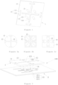
- a radiating structure 1 includes a radiating sheet 11 and a feeding column 14 for connecting the radiating sheet 11 and a feeding network (please refer to figure 3 ).
- the radiation sheet 11 may be a PCB or a metal sheet formed by etching a circuit, and a radiating slot 12 is defined in the middle potion of the radiation sheet 11.
- the radiating slot 12 includes a lateral slot 121 and a longitudinal slot 122 that are communicated with each other and are cross-orthogonal, and the lengths of the lateral slot 121 and the longitudinal slot 122 are both smaller than the lengths of the radiating sheet in corresponding extending directions of the corresponding radiating slots. That is, the radiation slot 12 is of a closed structure.
- the external radiation window of the radiating structure 1 can be increased, thereby reducing the Q value (Quality factor) of the antenna adopting the radiating structure 1, which is helpful to broaden the working frequency band.
- defining a slot on the radiating sheet 11 can also extend the path of the circuit distribution, reduce the resonance frequency of the radiating structure 1, and achieve the purpose of miniaturization.
- the lateral slot 121 and the longitudinal slot 122 arranged in a cross orthogonally can restrict the distribution of current, form two current modes with close resonance frequencies, and achieve the design purpose of broadband.
- the current distribution can be restricted by the radiating slot 12 arranged in a cross shape, and the polarization purity of the radiation field can also be improved, so as to achieve the purpose of improving the cross-polarization suppression ratio.
- the lateral slot 121 and the longitudinal slot 122 of the radiating slot 12 respectively extend along a direction which is at an angle of ⁇ 45° with respect to a polarization direction of the radiating sheet 11.
- the lateral slot 121 and the longitudinal slot 122 communicate with each other, thereby reducing the common body between the two polarization directions on the radiator 11, so as to reduce the electromagnetic coupling between the two polarization directions, and therefore, the isolation between the two polarization directions of the radiating structure 1 can be improved.
- the radiation from adjacent slots of the radiating slot 12 can be synthesized into radiation along a polarization direction between adjacent slots through vector synthesis, and its synthesized length is not less than the length of the radiator 11 in the polarization direction. Therefore, the radiation through vector synthesis of the radiating slot 12 having the cross structure can be superimposed on the radiation along the polarization direction, thereby improving the radiation efficiency.
- the intersection of the lateral slot 121 and the longitudinal slot 122 is located at the geometric center of the radiating sheet 11, and the lengths of the lateral slot 121 and the longitudinal slot 122 are both 0.7 ⁇ , and here, ⁇ is related to the working center frequency of the antenna.
- the radiation length, after vector synthesis, of the lateral slot 121 and the longitudinal slot 122 with a length of 0.7 ⁇ in the polarization direction between the two is equal to the length of the radiator 11 in the polarization direction.
- the radiating structure of the present application in addition to the radiation generated between the inherent outer edge of the radiation sheet 11 and a reflector plate 300, by defining the radiating slot 12 on the radiation sheet 11, the radiation of the cross structure can be added, so that the radiating structure 1 can generate two kinds of radiation simultaneously, so as to achieve the effect of polarization vector superposition enhancement, improve the radiation efficiency of the antenna unit, and further improve the radiation gain of the antenna. Therefore, only one radiating sheet 11 is required to achieve the same radiation efficiency and radiation gain of the traditional antenna adopting the multilayer patch structure, which can reduce the use of antenna components, the structure is simple, and the antenna profile can be reduced, which is helpful to realize the miniaturization of the antenna.
- the length or shape of the lateral slot 121 and the longitudinal slot 122 of the radiating slot 12 can also be changed to reduce errors caused by environmental or processing factors in actual processing and production. This ensures the symmetry of the pattern in the symmetry plane of the antenna, thereby ensuring the radiation efficiency of the antenna and improving the gain of the antenna.
- the radiating sheet 11 may have a symmetrical structure such as a square or a circle, or the radiating sheet 11 may be further provided with a hollow structure that is not communicated with the radiating slot 12, thereby reducing the weight of the radiator 11, in order to achieve the purpose of simple structure and light weight of the antenna unit with the radiating structure 1.
- this is beneficial to reduce the mutual coupling between the radiating structures 1 and play a role in improving the isolation and improving the pattern.
- an outer edge of the radiating sheet 11 is provided with at least one groove 13, and the groove 13 is not communicated with the radiating slot 12.
- the size of the grooves is smaller than 1 8 ⁇ , where ⁇ is related to the working center frequency of the antenna.
- the radiating sheet 11 of the present application has a smaller projected area, reduces the weight of the radiation sheet, can further reduce the common body between the two polarization directions of the radiating sheet 11, thereby achieving the purpose of improving the isolation between the polarization ports of the adjacent radiating structures 1 in the array.
- the groove 13 includes a notch portion 131 and an elongated portion 132 communicating with the notch portion 131.
- the notch portion 131 is formed by extending inwardly from the outer edge of the radiating sheet 11, and the elongated portion 132 is perpendicular to the notch portion 131.
- the edge length of the groove 13 can be further extended, so as to further extend the equivalent electrical length of the outer edge of the radiating sheet 11.
- the purpose of adjusting the radiation of the radiation sheet 11 in different polarization directions can also be achieved by adjusting the location of the elongated portion 132.
- each group of the feeding columns 14 includes two feeding columns 14 arranged along an axis of a corresponding polarization direction. Further, the location and length of the feeding column 14 can be adjusted according to actual conditions. The location of the feeding column 14 is adjusted to achieve the purpose of improving the symmetry of the antenna radiation pattern.
- the feeding column 14 and the radiating sheet 11 are integrally formed. Therefore, the stability of the connection between the feeding structure 2 and the radiating structure 1 is further improved.
- the feeding column 14 and the radiating sheet 11 can be connected by welding or snapping, which is convenient for production.
- the microstrip antenna unit includes a feeding structure 2 and a radiating structure 1 electrically connected to the feeding structure 2, and the radiating structure is the radiating structure 1 mentioned above.
- the radiating structure 1 in this embodiment is only one layer of radiating sheet 11. Therefore, applying the same to the microstrip antenna unit 100 can realize the low-profile design of the microstrip antenna unit 100, with a simple structure and reducing components, and this is helpful for the miniaturization of the antenna.
- the feeding structure 2 includes a feeding network 21 including a dielectric substrate plate 212 and a feeding line 211 provided on the dielectric substrate plate 212 and connected to the feeding column 14.
- a ground layer 213 is provided on the other side of the dielectric substrate plate 212 facing the side where the feeder line 211 is provided.
- the ground layer 213 in this embodiment is a metal floor.
- the dielectric substrate plate 212 of the feeding network 21 is a PCB board with a thickness of 1 mm and a dielectric constant of 3.0.
- the radiating structure 1 includes a radiating sheet 11 and a feeding column 14 for connecting the radiating sheet 11 and the feeding network 21.
- the feeding line 211 is directly electrically connected to the feeding column 14 to realize the feeding of the microstrip antenna unit 100.
- the structure is simple, no components are required, and the low profile of the antenna can be realized. This contributes to miniaturization of the antenna.
- the radiation generated between the outer edge of the radiating sheet 11 and the reflector plate 300 is in a parallel structure relationship with the radiation generated by the radiating slot 12, and the radiation currents generated by the two can be combined in the feeding column 14 to realize power feeding, to achieve the purpose of parallel resonance, thereby achieving the effect of widening the working bandwidth.
- the microstrip antenna unit 100 of the present application is provided with a radiating slot 12 on the radiation sheet 11, and the radiation generated by the radiation slot 12 and the radiation from the inherent outer edge of the radiation sheet 11 are merged through the feeding column 14 to form a parallel structure, and this makes the microstrip antenna unit 100 have a wider working frequency band.
- the connection between the radiating structure 1 and the feeding structure 2 does not require additional components for fastening and interconnection, so there are fewer antenna components, thereby achieving the effects of miniaturization, low profile, and light weight.
- the bandwidth required by the microstrip antenna can be realized only by the radiating sheet 11 with a simple structure, and the isolation of the microstrip antenna can be improved, thereby increasing the radiation gain of the antenna.
- the present application also relates to an array antenna.
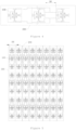
- it includes a reflector plate 300 and at least one antenna array provided on the reflector plate 300, and a plurality of the above-mentioned microstrip antenna units are disposed in the antenna array 100.
- each antenna array has at least one sub-module (not shown in the figure).
- Each of the sub-modules includes a plurality of microstrip antenna units 100 connected by a plurality of feeding networks 21.
- the feeding networks 21 of the microstrip antenna unit 100 in the sub-module are connected by a microstrip line/strip line power dividing network (not shown in the figure) or a coaxial feeding line.
- the sub-module in this embodiment includes three microstrip antenna units 100 arranged in a longitudinal direction, and the three microstrip antenna units 100 are connected by a ⁇ 45° polarized power dividing network.
- the vertical spacing of the three microstrip antenna units DV 0.5-1.0 ⁇ , where ⁇ is related to the working center frequency of the antenna.
- An array antenna of this embodiment consists of 3 row X 8 column of sub-modules, and each column of sub-modules constitutes an antenna array.
- a decoupling isolation strip 200 is provided between the antenna arrays of two adjacent columns, which can reduce the mutual coupling between the antenna sub-modules in the antenna working frequency band, thereby improving the isolation of the antenna sub-modules between adjacent columns, and it has little impact on other performance indicators of the antenna.
- figure 6 shows a simulation curve diagram of the voltage standing wave ratio of the microstrip antenna unit 100 of the present application in the working frequency band.
- the figure shows that the microstrip antenna unit 100 has an impedance bandwidth of more than 20% when the standing wave ratio is less than 2, and this indicates that the microstrip antenna unit 100 has a wider impedance bandwidth under the premise of ensuring the radiation efficiency of the antenna.
- Figure 7 is a graph of isolation of the same polarization ports of the array antenna of the present application. That is, in the frequency range of 2.30GHz-3.00GHz, the isolation of the same polarization is greater than 23dB.
- Figure 8 is a graph of isolation of different polarization ports of the array antenna of the present application. That is, in the frequency range of 2.30GHz-3.00GHz, the isolation of the same polarization is greater than 35dB.
Landscapes
- Engineering & Computer Science (AREA)
- Computer Networks & Wireless Communication (AREA)
- Waveguide Aerials (AREA)
- Variable-Direction Aerials And Aerial Arrays (AREA)
Description
- This application relates to the field of mobile communication antennas, in particular to a radiating structure, a microstrip antenna unit and an array antenna.
- With the refined and deep coverage of mobile communication networks, the trial commercial use of 5G networks, the deployment of large-scale array antennas in the future, and the development of base station master equipment and antennas toward the gradual integration of antennas, the communication system puts forward higher requirements for the miniaturization and light weight of the antenna.
- In 5G communication technology, the first problem to be solved is how to realize the design of large-scale and lightweight array antennas. In a traditional MIMO system, the distance between the antennas is large and the mutual coupling is weak. Therefore, it is often possible to use metal die-cast dipoles with relatively stable structure and performance, but with a large volume and mass. However, in a 5G massive MIMO system, the base station needs to deploy a large number of array antenna units in a given space, and the total weight of the AAU equipment formed by the integration of the main equipment of the base station and the antenna also poses a greater challenge to the load-bearing capacity of the pillar. At this time, the die-cast dipole of the traditional base station antenna is not suitable for the needs of the communication system due to its large volume and heavy mass. In addition, the traditional die-cast dipoles are used in 5G large-scale dense arrays. Due to their large size and obvious mutual coupling effect, the antenna performance will deteriorate.
- The microstrip antenna itself has the advantages of low profile and light weight, and is more suitable for use in 5G large-scale array antennas. In order to solve the mutual coupling effect, that is, the problem of isolation between antenna ports, or to solve the problem of working bandwidth, the main measure of the microstrip antenna is to adopt a double-layer patch solution. That is, a radiation patch is combined with a parasitic patch, and the patches are interconnected by a plastic holding member and fastened to a reflector plate. Or, these patches are printed on a multi-layer PCB board, so that while the existing microstrip antenna obtains corresponding performance, it will also cause problems such as an increase in the number of parts of the array antenna, a complex assembly, and a higher profile.
- Chinese patent publication No.
CN103618149A , entitled "DOUBLE-POLARIZED RADIATION UNIT AND ANTENNA" discloses a double-polarized radiation unit and an antenna. The double-polarized radiation unit comprises two pairs of radiation bodies arranged in a mutually orthogonal mode, a base installed on lower portions of the radiation bodies and a metal baffle board installed on the lower portion of the base. Each radiation body is sequentially provided with at least three dipoles from the center to an outer circle, each dipole comprises two corresponding half-dipoles, and the half-dipole on the outermost side and an adjacent polarized half-dipole form a closed electromagnetic loop. - European patent publication No.
EP3454414A1 , entitled "BROADBAND LOW-PROFILE DUAL-LINEARLY POLARIZED ANTENNA FOR A ONELTE TWO-IN-ONE PLATFORM" discloses a broadband low-profile dual-linearly polarized antenna for a OneLTE two-in-one platform and an antenna array device formed therefrom are provided that can realize low-profile and ultra-broadband and have such advantages as simple structure, neat appearance, easy engineering implementation, and suitability for mass production. The broadband low-profile dual-linearly polarized antenna can include a radiating portion that can include a dielectric substrate, printed folded dipoles spaced apart on an upper surface of the dielectric substrate, first coupled parasitic elements on a lower surface of the dielectric substrate, and second coupled parasitic elements on the upper surface of the dielectric substrate and a feed balun for feeding the radiating portion, wherein each of the printed folded dipoles can include a corresponding one of the first coupled parasitic elements and a corresponding one of the second coupled parasitic elements. - Chinese patent publication No.
CN106329083A , entitled "COMPACT MICROSTRIP ANTENNA" discloses a compact microstrip antenna, which comprises a dielectric layer, a radiation patch, and a grounding part formed on the upper surface and the lower surface of the dielectric layer, wherein gaps are opened in the radiation patch; and the gaps comprise a cross-shaped first gap, and four cross-shaped second gaps symmetrically distributed around the first gap. - A primary object of this application is to provide a radiating structure suitable for the development of the 5G era, with simple structure and low-profile characteristics.
- Another object of the present application is to provide an array antenna including the above-mentioned radiating structure.
- In order to achieve the above objects, this application provides the following technical solution:
- As a first aspect, the present application relates to a radiating structure, which includes a radiation sheet, and a radiating slot is defined in a middle portion of the radiation sheet, the radiating slot includes a lateral slot and a longitudinal slot that are communicated with each other and are cross-orthogonal, and the lengths of the lateral slot and the longitudinal slot are both smaller than the lengths of the radiating sheet in corresponding extending directions of the corresponding radiating slots. At least one groove is provided on an outer edge of the radiating sheet, and the groove is not communicated with the radiating slot, wherein the groove is disposed at a location corresponding to an end portion of the radiating slot.
- Preferably, the lateral slot and the longitudinal slot respectively extend along a direction which is at an angle of ±45° with respect to a polarization direction of the radiating structure.
- Preferably , a vector synthesized length of two adjacent slots of the radiating slot in a polarization direction between the two adjacent slots is not less than a length of the radiation sheet in the polarization direction.
- Preferably, the groove includes a notch portion extending inward from the outer edge of the radiating sheet and an elongated portion perpendicular to the notch portion and communicating with the notch portion.
- Preferably, it further comprises a feeding column for connecting the radiating sheet and a feeding network.
- Preferably, corresponding to two polarization directions of the radiating sheet, two groups of the feeding columns are respectively provided, and each group of the feeding columns includes two feeding columns arranged along an axis of a corresponding polarization direction.
- Preferably, the feeding column and the radiating sheet are integrally formed; or the power feeding column and the radiating sheet are welded or snap- connected.
- Preferably, the radiating sheet is provided with several hollow structures.
- As a second aspect, the present application also relates to an array antenna, including a reflector plate and at least one antenna array provided on the reflector plate, and each antenna array is provided with a plurality of the above-mentioned radiating structures.
- Preferably, a decoupling isolation strip is provided between two adjacent antenna arrays.
- Compared with the prior art, the solution of this application has the following advantages:
- 1. In the radiating structure of the present application, by defining a radiating slot on the radiation sheet, the radiation sheet not only has the radiation generated between its own outer edge and the antenna reflector plate, but also has the radiation of the radiating slot. When the radiating structure works in the antenna system, it can generate two kinds of radiation simultaneously, achieving the effect of polarization vector superposition and enhancement. By increasing an external radiation window of the radiation sheet, the Q value of the microstrip radiating structure can be reduced, which is helpful to broadening the working frequency band. By opening the radiating slot, the current distribution can be restrained, thereby improving the polarization purity of the radiation field, thereby achieving the purpose of improving the antenna cross-polarization suppression ratio. That is, only one layer of radiating sheet is required to achieve the same radiation efficiency and radiation gain of the traditional antenna adopting the multilayer patch structure, thereby reducing the use of parts, its structure is simple, and the antenna profile can be reduced, which is beneficial to the realization the miniaturization of the antenna.
- 2. In the radiating structure of the present application, mutually communicated later slot and longitudinal slot are defined on the radiating sheet, which can reduce the common body in the two polarization directions on the radiating sheet, so as to achieve the purpose of reducing the electromagnetic coupling between the two polarizations. Therefore, the isolation between the two polarization directions of the radiating structure can be improved.
- 3. In the radiating structure of the present application, the equivalent electrical length of the outer edge of the radiator is extended by arranging grooves on the outer edge of the radiator. Compared with the radiating structure of the traditional microstrip antenna unit, the radiation sheet of the present application has a smaller projected area, which can further reduce the common body between the two polarization directions of the radiation sheet. Therefore, the purpose of improving the isolation between the polarization ports of adjacent radiating structures in the array is achieved.
- 4. In the radiating structure of the present application, a radiating slot is provided on the radiation sheet, and the radiation generated by the radiating slot and the radiation on the inherent outer edge of the radiation sheet are merged through the feeding column to form a parallel structure, making the microstrip antenna unit have a wider working frequency band. In addition, the connection between the radiating structure and the feeding structure does not require additional components for fastening and interconnection, so the antenna has fewer components to achieve the effect of miniaturization, low profile, and light weight. In addition, the bandwidth required by the microstrip antenna can be realized by only one layer of radiating sheet with a simple structure, and the isolation of the microstrip antenna can be improved, thereby increasing the radiation gain of the antenna.
- The additional aspects and advantages of this application will be partly given in the following description, which will become obvious from the following description, or be understood through the practice of this application.
- The above and/or additional aspects and advantages of the present application will become obvious and easy to understand from the following description of the embodiments in conjunction with the accompanying drawings, in which:
-
Figure 1 is a schematic structural diagram of an embodiment of a radiating structure of this application; -
Figures 2a-2c are schematic diagrams of various implementation structures of the radiating structure of this application; -
Figure 3 is a schematic structural diagram of an embodiment of a microstrip antenna unit of this application; -
Figure 4 is a schematic structural diagram of an antenna sub-module in the array antenna of this application; -
Figure. 5 is a schematic structural diagram of an embodiment of an array antenna according to this application; -
Figure 6 is a simulation curve diagram of the voltage standing wave ratio of the microstrip antenna unit of the application in the working frequency band; -
Figure 7 is a graph of isolation of the same polarization ports of the array antenna of the present application; and -
Figure 8 is a graph of isolation of different polarization ports of the array antenna of the present application. - In the figure drawings, 1 represents a radiating structure; 11 represents a radiating sheet; 12 represents a radiation slot; 121 represents a lateral slot; 122 represents a longitudinal slot; 13 represents a groove; 131 represents a notch portion; 132 represents an elongated portion; 14 represents a feeding column; 2 represents a feeding structure; 21 represents a feeding network; 211 represents a feeding line; 212 represents a dielectric substrate plate; 213 represents a ground layer; 100 represents a microstrip antenna unit; 200 represents a decoupling strip; and 300 represents a reflector plate.
- The embodiments of the present application are described in detail below. Examples of the embodiments are shown in the accompanying drawings, wherein the same or similar reference numerals indicate the same or similar elements or elements with the same or similar functions. The embodiments described below with reference to the drawings are exemplary, and are only used to explain the present application, and cannot be construed as a limitation to the present application.
- Please refer to
figures 1 to 8 . This application relates to a radiating structure mainly used in the field of mobile communication antennas. By applying the radiatingstructure 1 to an antenna structure, the polarization isolation of the antenna can be improved, and the structure is simple, and it has low profile characteristics, which is helpful to miniaturization. It can provide reliable resources for the refined and deep coverage of mobile communication networks and the development of the 5G era. - Please refer to
figure 1 , a radiatingstructure 1 includes a radiatingsheet 11 and afeeding column 14 for connecting the radiatingsheet 11 and a feeding network (please refer tofigure 3 ). Here, theradiation sheet 11 may be a PCB or a metal sheet formed by etching a circuit, and a radiatingslot 12 is defined in the middle potion of theradiation sheet 11. - Preferably, the radiating
slot 12 includes alateral slot 121 and alongitudinal slot 122 that are communicated with each other and are cross-orthogonal, and the lengths of thelateral slot 121 and thelongitudinal slot 122 are both smaller than the lengths of the radiating sheet in corresponding extending directions of the corresponding radiating slots. That is, theradiation slot 12 is of a closed structure. - By defining the radiating
slot 12 with a closed structure on the radiatingsheet 11, the external radiation window of the radiatingstructure 1 can be increased, thereby reducing the Q value (Quality factor) of the antenna adopting the radiatingstructure 1, which is helpful to broaden the working frequency band. In addition, defining a slot on the radiatingsheet 11 can also extend the path of the circuit distribution, reduce the resonance frequency of the radiatingstructure 1, and achieve the purpose of miniaturization. In addition, thelateral slot 121 and thelongitudinal slot 122 arranged in a cross orthogonally can restrict the distribution of current, form two current modes with close resonance frequencies, and achieve the design purpose of broadband. At the same time, the current distribution can be restricted by the radiatingslot 12 arranged in a cross shape, and the polarization purity of the radiation field can also be improved, so as to achieve the purpose of improving the cross-polarization suppression ratio. - In a preferred embodiment, the
lateral slot 121 and thelongitudinal slot 122 of the radiatingslot 12 respectively extend along a direction which is at an angle of ±45° with respect to a polarization direction of the radiatingsheet 11. In addition, thelateral slot 121 and thelongitudinal slot 122 communicate with each other, thereby reducing the common body between the two polarization directions on theradiator 11, so as to reduce the electromagnetic coupling between the two polarization directions, and therefore, the isolation between the two polarization directions of the radiatingstructure 1 can be improved. - In a further preferred embodiment, the radiation from adjacent slots of the radiating
slot 12 can be synthesized into radiation along a polarization direction between adjacent slots through vector synthesis, and its synthesized length is not less than the length of theradiator 11 in the polarization direction. Therefore, the radiation through vector synthesis of the radiatingslot 12 having the cross structure can be superimposed on the radiation along the polarization direction, thereby improving the radiation efficiency. Preferably, in this embodiment, the intersection of thelateral slot 121 and thelongitudinal slot 122 is located at the geometric center of the radiatingsheet 11, and the lengths of thelateral slot 121 and thelongitudinal slot 122 are both 0.7λ, and here, λ is related to the working center frequency of the antenna. The radiation length, after vector synthesis, of thelateral slot 121 and thelongitudinal slot 122 with a length of 0.7λ in the polarization direction between the two is equal to the length of theradiator 11 in the polarization direction. - In the radiating structure of the present application, in addition to the radiation generated between the inherent outer edge of the
radiation sheet 11 and areflector plate 300, by defining the radiatingslot 12 on theradiation sheet 11, the radiation of the cross structure can be added, so that the radiatingstructure 1 can generate two kinds of radiation simultaneously, so as to achieve the effect of polarization vector superposition enhancement, improve the radiation efficiency of the antenna unit, and further improve the radiation gain of the antenna. Therefore, only one radiatingsheet 11 is required to achieve the same radiation efficiency and radiation gain of the traditional antenna adopting the multilayer patch structure, which can reduce the use of antenna components, the structure is simple, and the antenna profile can be reduced, which is helpful to realize the miniaturization of the antenna. - In a preferred embodiment, the length or shape of the
lateral slot 121 and thelongitudinal slot 122 of the radiatingslot 12 can also be changed to reduce errors caused by environmental or processing factors in actual processing and production. This ensures the symmetry of the pattern in the symmetry plane of the antenna, thereby ensuring the radiation efficiency of the antenna and improving the gain of the antenna. - In addition, referring to
figures 2a to 2c , the radiatingsheet 11 may have a symmetrical structure such as a square or a circle, or the radiatingsheet 11 may be further provided with a hollow structure that is not communicated with the radiatingslot 12, thereby reducing the weight of theradiator 11, in order to achieve the purpose of simple structure and light weight of the antenna unit with the radiatingstructure 1. In addition, in the design of an array antenna with a relatively close unit spacing, this is beneficial to reduce the mutual coupling between the radiatingstructures 1 and play a role in improving the isolation and improving the pattern. - According to the invention, an outer edge of the radiating
sheet 11 is provided with at least onegroove 13, and thegroove 13 is not communicated with the radiatingslot 12. Preferably, in this embodiment, there are 4grooves 13 that are respectively disposed at locations corresponding to end portions of the radiatingslot 12. That is, thegrooves 13 are located in areas defined between the two polarization directions of the radiatingsheet 11. - In a further preferred embodiment, the size of the grooves is smaller than

- By arranging the
grooves 13 on the outer edge of the radiatingsheet 11, the equivalent electrical length of the outer edge of the radiatingsheet 11 can be extended. Compared with the radiatingstructure 1 of a traditionalmicrostrip antenna unit 100, the radiatingsheet 11 of the present application has a smaller projected area, reduces the weight of the radiation sheet, can further reduce the common body between the two polarization directions of the radiatingsheet 11, thereby achieving the purpose of improving the isolation between the polarization ports of theadjacent radiating structures 1 in the array. - Preferably, the
groove 13 includes anotch portion 131 and anelongated portion 132 communicating with thenotch portion 131. Thenotch portion 131 is formed by extending inwardly from the outer edge of the radiatingsheet 11, and theelongated portion 132 is perpendicular to thenotch portion 131. By defining theelongated portion 132 communicating with thenotch portion 131, the edge length of thegroove 13 can be further extended, so as to further extend the equivalent electrical length of the outer edge of the radiatingsheet 11. In addition, the purpose of adjusting the radiation of theradiation sheet 11 in different polarization directions can also be achieved by adjusting the location of theelongated portion 132. - Please refer to
figures 1-2 . Corresponding to two polarization directions of the radiatingsheet 11, two groups of thefeeding columns 14 are respectively provided, and each group of thefeeding columns 14 includes two feedingcolumns 14 arranged along an axis of a corresponding polarization direction. Further, the location and length of thefeeding column 14 can be adjusted according to actual conditions. The location of thefeeding column 14 is adjusted to achieve the purpose of improving the symmetry of the antenna radiation pattern. - In a preferred embodiment, the
feeding column 14 and the radiatingsheet 11 are integrally formed. Therefore, the stability of the connection between the feedingstructure 2 and the radiatingstructure 1 is further improved. - In another preferred embodiment, the
feeding column 14 and the radiatingsheet 11 can be connected by welding or snapping, which is convenient for production. - This application also relates to a microstrip antenna unit, and please refer to
figure 3 , the microstrip antenna unit includes afeeding structure 2 and a radiatingstructure 1 electrically connected to thefeeding structure 2, and the radiating structure is the radiatingstructure 1 mentioned above. By applying the radiatingstructure 1 to themicrostrip antenna unit 100, its working bandwidth can be broadened, and the radiation efficiency can be improved. In addition, the radiatingstructure 1 in this embodiment is only one layer of radiatingsheet 11. Therefore, applying the same to themicrostrip antenna unit 100 can realize the low-profile design of themicrostrip antenna unit 100, with a simple structure and reducing components, and this is helpful for the miniaturization of the antenna. - The feeding
structure 2 includes afeeding network 21 including adielectric substrate plate 212 and afeeding line 211 provided on thedielectric substrate plate 212 and connected to thefeeding column 14. Aground layer 213 is provided on the other side of thedielectric substrate plate 212 facing the side where thefeeder line 211 is provided. Specifically, theground layer 213 in this embodiment is a metal floor. - In a preferred embodiment, the
dielectric substrate plate 212 of thefeeding network 21 is a PCB board with a thickness of 1 mm and a dielectric constant of 3.0. - The radiating
structure 1 includes a radiatingsheet 11 and afeeding column 14 for connecting the radiatingsheet 11 and thefeeding network 21. Thefeeding line 211 is directly electrically connected to thefeeding column 14 to realize the feeding of themicrostrip antenna unit 100. The structure is simple, no components are required, and the low profile of the antenna can be realized. This contributes to miniaturization of the antenna. - The radiation generated between the outer edge of the radiating
sheet 11 and thereflector plate 300 is in a parallel structure relationship with the radiation generated by the radiatingslot 12, and the radiation currents generated by the two can be combined in thefeeding column 14 to realize power feeding, to achieve the purpose of parallel resonance, thereby achieving the effect of widening the working bandwidth. - Based on the above structure, compared with the traditional microstrip antenna, the
microstrip antenna unit 100 of the present application is provided with a radiatingslot 12 on theradiation sheet 11, and the radiation generated by theradiation slot 12 and the radiation from the inherent outer edge of theradiation sheet 11 are merged through thefeeding column 14 to form a parallel structure, and this makes themicrostrip antenna unit 100 have a wider working frequency band. In addition, the connection between the radiatingstructure 1 and thefeeding structure 2 does not require additional components for fastening and interconnection, so there are fewer antenna components, thereby achieving the effects of miniaturization, low profile, and light weight. Moreover, the bandwidth required by the microstrip antenna can be realized only by the radiatingsheet 11 with a simple structure, and the isolation of the microstrip antenna can be improved, thereby increasing the radiation gain of the antenna. - The present application also relates to an array antenna. Referring to
figures 4 and 5 , it includes areflector plate 300 and at least one antenna array provided on thereflector plate 300, and a plurality of the above-mentioned microstrip antenna units are disposed in theantenna array 100. - As a preferred embodiment, each antenna array has at least one sub-module (not shown in the figure). Each of the sub-modules includes a plurality of
microstrip antenna units 100 connected by a plurality of feedingnetworks 21. In addition, thefeeding networks 21 of themicrostrip antenna unit 100 in the sub-module are connected by a microstrip line/strip line power dividing network (not shown in the figure) or a coaxial feeding line. Specifically, the sub-module in this embodiment includes threemicrostrip antenna units 100 arranged in a longitudinal direction, and the threemicrostrip antenna units 100 are connected by a ±45° polarized power dividing network. In addition, the vertical spacing of the three microstrip antenna units DV=0.5-1.0λ, where λ is related to the working center frequency of the antenna. - It should be understood that if the number of
microstrip antenna units 100 in each sub-module is N (N≥3), in the same antenna sub-module, input ends of the +45°polarized feeding networks 21 of themicrostrip antenna units 100 are electrically connected through a one-to-N power dividing network, and input ends of the -45°polarized feeding networks 21 of themicrostrip antenna units 100 are electrically connected through a one-to-N power dividing network. - As a preferred embodiment, please refer to
Figure 5 . An array antenna of this embodiment consists of 3 row X 8 column of sub-modules, and each column of sub-modules constitutes an antenna array. In addition, the distance between two adjacent columns of antenna arrays is DH=0.45-0.75λ, where λ is related to the antenna working center frequency. In addition, adecoupling isolation strip 200 is provided between the antenna arrays of two adjacent columns, which can reduce the mutual coupling between the antenna sub-modules in the antenna working frequency band, thereby improving the isolation of the antenna sub-modules between adjacent columns, and it has little impact on other performance indicators of the antenna. - The application effects of this application will be described in detail below in conjunction with simulation.
-
figure 6 shows a simulation curve diagram of the voltage standing wave ratio of themicrostrip antenna unit 100 of the present application in the working frequency band. The figure shows that themicrostrip antenna unit 100 has an impedance bandwidth of more than 20% when the standing wave ratio is less than 2, and this indicates that themicrostrip antenna unit 100 has a wider impedance bandwidth under the premise of ensuring the radiation efficiency of the antenna. -
Figure 7 is a graph of isolation of the same polarization ports of the array antenna of the present application. That is, in the frequency range of 2.30GHz-3.00GHz, the isolation of the same polarization is greater than 23dB. -
Figure 8 is a graph of isolation of different polarization ports of the array antenna of the present application. That is, in the frequency range of 2.30GHz-3.00GHz, the isolation of the same polarization is greater than 35dB. - The above are only part of the implementation of this application. It should be pointed out that for those of ordinary skill in the art, without departing from the scope of the appended claims, several improvements and modifications can be made, and these improvements and modifications are also regarded as the scope of protection of this application.
Claims (10)
- A radiating structure (1) , comprising a radiating sheet (11) , wherein a radiating slot (12) is defined in a middle portion of the radiating sheet (11) , the radiating slot (12) includes a lateral slot (121) and a longitudinal slot (122) that are communicated with each other and are cross-orthogonal, and the lengths of the lateral slot (121) and the longitudinal slot (122) are both smaller than the lengths of the radiating sheet (11) in corresponding extending directions of the corresponding radiating slots (12) ;
characterized in that
at least one groove (13) is provided on an outer edge of the radiating sheet (11) , and the groove (13) is not communicated with the radiating slot (12) , and the groove (13) is disposed at a location corresponding to an end portion of the radiating slot (12) . - The radiating structure (1) as recited in claim 1, wherein the lateral slot (121) and the longitudinal slot (122) respectively extend along a direction which is at an angle of ±45° with respect to a polarization direction of the radiating structure (1) .
- The radiating structure (1) as recited in claim 2, wherein a vector synthesized length of two adjacent slots of the radiating slot (12) in a polarization direction between the two adjacent slots is not less than a length of the radiation sheet (11) in the polarization direction.
- The radiating structure (1) as recited in claim 1, wherein the groove (13) includes a notch portion (131) extending inward from the outer edge of the radiating sheet (11) and an elongated portion (132) perpendicular to the notch portion (131) and communicating with the notch portion (131) .
- The radiating structure (1) as recited in claim 1, further comprising a feeding column (14) for connecting the radiating sheet (11) and a feeding network.
- The radiating structure (1) as recited in claim 5, wherein corresponding to two polarization directions of the radiating sheet (11) , two groups of the feeding columns (14) are respectively provided, and each group of the feeding columns (14) includes two feeding columns (14) arranged along an axis of a corresponding polarization direction.
- The radiating structure (1) as recited in claim 5, wherein the feeding column (14) and the radiating sheet (11) are integrally formed; or the power feeding column (14) and the radiating sheet (11) are welded or snap- connected.
- The radiating structure (1) as recited in any one of claims 1-7, wherein the radiating sheet (11) is provided with several hollow structures.
- An array antenna, comprising a reflector plate (300) and at least one antenna array provided on the reflector plate, and each antenna array is provided with a plurality of radiating structures (1) as recited in any one of claims 1-8.
- The array antenna as recited in claim 9, wherein a decoupling isolation strip (200) is provided between two adjacent antenna arrays.
Applications Claiming Priority (2)
| Application Number | Priority Date | Filing Date | Title |
|---|---|---|---|
| CN201910407059.5A CN110098477B (en) | 2019-05-16 | 2019-05-16 | Radiation structure and array antenna |
| PCT/CN2019/117111 WO2020228275A1 (en) | 2019-05-16 | 2019-11-11 | Radiating structure and array antenna |
Publications (4)
| Publication Number | Publication Date |
|---|---|
| EP3968458A1 EP3968458A1 (en) | 2022-03-16 |
| EP3968458A4 EP3968458A4 (en) | 2022-07-20 |
| EP3968458C0 EP3968458C0 (en) | 2023-08-30 |
| EP3968458B1 true EP3968458B1 (en) | 2023-08-30 |
Family
ID=67448315
Family Applications (1)
| Application Number | Title | Priority Date | Filing Date |
|---|---|---|---|
| EP19928598.2A Active EP3968458B1 (en) | 2019-05-16 | 2019-11-11 | Radiating structure and array antenna |
Country Status (3)
| Country | Link |
|---|---|
| EP (1) | EP3968458B1 (en) |
| CN (1) | CN110098477B (en) |
| WO (1) | WO2020228275A1 (en) |
Families Citing this family (20)
| Publication number | Priority date | Publication date | Assignee | Title |
|---|---|---|---|---|
| CN110098477B (en) * | 2019-05-16 | 2022-08-26 | 京信通信技术(广州)有限公司 | Radiation structure and array antenna |
| CN113994542A (en) | 2019-05-24 | 2022-01-28 | 康普技术有限责任公司 | Wireless communication system having patch antenna array supporting large scanning angle radiation |
| CN110768005A (en) * | 2019-10-29 | 2020-02-07 | 上海安费诺永亿通讯电子有限公司 | Dual-polarized antenna oscillator |
| CN112751180B (en) | 2019-10-31 | 2022-03-22 | Oppo广东移动通信有限公司 | Antenna module and electronic equipment |
| CN112751168B (en) * | 2019-10-31 | 2022-11-08 | Oppo广东移动通信有限公司 | Antenna module and electronic equipment |
| CN110768007B (en) * | 2019-11-15 | 2025-10-03 | 深圳市雨辰科技有限公司 | Combined planar oscillator near-field antenna |
| CN110943301B (en) * | 2019-12-12 | 2021-02-12 | 中国科学院长春光学精密机械与物理研究所 | Cross-scale dual-bandpass frequency selective surface and its periodic element, design method |
| CN111129735B (en) * | 2019-12-31 | 2022-09-27 | 京信通信技术(广州)有限公司 | Broadband radiation unit and array antenna |
| CN111585007B (en) * | 2020-05-08 | 2022-04-15 | 武汉虹信科技发展有限责任公司 | Highly integrated MIMO antenna |
| US20230318182A1 (en) * | 2020-08-13 | 2023-10-05 | Telefonaktiebolaget Lm Ericsson (Publ) | Antenna radiator, and antenna |
| CN112350060A (en) * | 2020-09-21 | 2021-02-09 | 昆山恩电开通信设备有限公司 | Low-profile high-performance integrated radiating unit |
| CN112397899A (en) * | 2020-11-27 | 2021-02-23 | 浙江盛洋科技股份有限公司 | 5G array antenna |
| CN112886196B (en) * | 2021-01-08 | 2023-12-19 | 深圳市信维通信股份有限公司 | Base station antenna and base station equipment |
| CN113540755B (en) * | 2021-06-24 | 2022-12-13 | 西安电子科技大学 | 5G dual-polarized base station antenna with high isolation characteristic and wide-angle scanning characteristic |
| CN113540823B (en) * | 2021-06-30 | 2022-11-18 | 上海航天电子有限公司 | Small Vivaldi array antenna with unevenly distributed loaded antenna housing |
| WO2023110068A1 (en) | 2021-12-15 | 2023-06-22 | Telefonaktiebolaget Lm Ericsson (Publ) | Radiator as well as antenna |
| CN117080715A (en) * | 2022-05-10 | 2023-11-17 | 安弗施技术公司 | Radiator, antenna and base station |
| CN115441154A (en) * | 2022-09-30 | 2022-12-06 | 武汉凡谷电子技术股份有限公司 | an antenna |
| CN116666974B (en) * | 2023-07-24 | 2023-09-22 | 南京纳特通信电子有限公司 | A doubly-fed polarization switchable ultra-wideband microstrip dipole antenna |
| CN120200016B (en) * | 2025-03-31 | 2026-05-01 | 太原理工大学 | Microstrip antenna device, navigation equipment and manufacturing method |
Family Cites Families (18)
| Publication number | Priority date | Publication date | Assignee | Title |
|---|---|---|---|---|
| FR2598036B1 (en) * | 1986-04-23 | 1988-08-12 | France Etat | PLATE ANTENNA WITH DOUBLE CROSS POLARIZATIONS |
| US6304226B1 (en) * | 1999-08-27 | 2001-10-16 | Raytheon Company | Folded cavity-backed slot antenna |
| US7999744B2 (en) * | 2007-12-10 | 2011-08-16 | City University Of Hong Kong | Wideband patch antenna |
| EP2081251B1 (en) * | 2008-01-15 | 2018-07-11 | HMD Global Oy | Patch antenna |
| JP4858566B2 (en) * | 2009-03-31 | 2012-01-18 | 三菱電機株式会社 | Antenna device |
| CN102610908A (en) * | 2012-03-01 | 2012-07-25 | 西安电子科技大学 | Ultra wide band four-tape circularly polarized antenna |
| CN103367920B (en) * | 2012-03-31 | 2016-08-03 | 深圳市金溢科技股份有限公司 | The OBU of microstrip antenna, electronic equipment and ETC system |
| CN103618149A (en) * | 2013-12-02 | 2014-03-05 | 江苏捷士通射频系统有限公司 | Double-polarized radiation unit and antenna |
| CN106329083A (en) * | 2015-06-15 | 2017-01-11 | 张家港贸安贸易有限公司 | Compact microstrip antenna |
| CN105119044B (en) * | 2015-09-09 | 2019-01-18 | 华为技术有限公司 | A kind of microstrip antenna and communication device |
| CN105846113B (en) * | 2016-05-25 | 2019-01-22 | 广东博纬通信科技有限公司 | A kind of dual-band and dual-polarization narrow beam array antenna |
| CN206059637U (en) * | 2016-07-19 | 2017-03-29 | 深圳市华信天线技术有限公司 | A kind of circular polarized antenna |
| CN207116699U (en) * | 2017-07-25 | 2018-03-16 | 上海汇珏网络通信设备有限公司 | A linear array antenna |
| EP3454414B1 (en) * | 2017-09-08 | 2020-05-27 | PC-Tel, Inc. | Broadband low-profile dual-linearly polarized antenna for a onelte two-in-one platform |
| CN108808231A (en) * | 2018-06-01 | 2018-11-13 | 电子科技大学 | A kind of dual polarization plane ultra wide band mimo antenna |
| CN109659677B (en) * | 2018-12-28 | 2024-08-13 | 华南理工大学 | Antenna and its radiating element |
| CN209804887U (en) * | 2019-05-16 | 2019-12-17 | 京信通信技术(广州)有限公司 | Radiation structure and array antenna |
| CN110098477B (en) * | 2019-05-16 | 2022-08-26 | 京信通信技术(广州)有限公司 | Radiation structure and array antenna |
-
2019
- 2019-05-16 CN CN201910407059.5A patent/CN110098477B/en active Active
- 2019-11-11 EP EP19928598.2A patent/EP3968458B1/en active Active
- 2019-11-11 WO PCT/CN2019/117111 patent/WO2020228275A1/en not_active Ceased
Also Published As
| Publication number | Publication date |
|---|---|
| CN110098477A (en) | 2019-08-06 |
| WO2020228275A1 (en) | 2020-11-19 |
| EP3968458A1 (en) | 2022-03-16 |
| EP3968458C0 (en) | 2023-08-30 |
| EP3968458A4 (en) | 2022-07-20 |
| CN110098477B (en) | 2022-08-26 |
Similar Documents
| Publication | Publication Date | Title |
|---|---|---|
| EP3968458A1 (en) | Radiating structure and array antenna | |
| US8866688B2 (en) | Dual-polarized radiation element and planar oscillator thereof | |
| US8269682B2 (en) | Multi-loop antenna module with wide beamwidth | |
| US8482471B2 (en) | Hybrid multiple-input multiple-output antenna module and system of using the same | |
| CN107230840B (en) | High gain broadband microstrip patch antenna | |
| US20200412002A1 (en) | Antenna Element and Array Antenna | |
| CN111541010B (en) | A 5G low-profile dual-polarization radiating unit and base station antenna | |
| CN116895953B (en) | A dual-polarization ultra-wide bandwidth angular scanning tightly coupled curved array antenna | |
| EP4044373B1 (en) | Omnidirectional dual-polarized antenna and communication device | |
| CN116565557A (en) | A wide-angle scanning ultra-wideband dual-polarization phased array antenna | |
| CN211829186U (en) | 5G low-profile dual-polarized radiation unit and base station antenna | |
| US12136767B2 (en) | Antenna assembly and base station antenna | |
| US20240235058A1 (en) | Decoupling device and decoupling method | |
| CN112670704A (en) | Oblique 45-degree polarized radiation broadband tile-type phased array antenna | |
| CN112688070B (en) | Distributed multi-point feed broadband vertical polarization omnidirectional antenna | |
| US20220294116A1 (en) | Radiation element for antenna and antenna including the radiation element | |
| CN113708051A (en) | Radiation unit, antenna and base station | |
| CN113036404A (en) | Low-profile ultra-wideband dual-polarized antenna element, antenna array and base station equipment | |
| CN209822857U (en) | Novel tightly-fed broadband dual-polarization butterfly-shaped oscillator | |
| CN116154490A (en) | Ultra-wideband tight coupling wide-angle scanning array antenna | |
| CN219180766U (en) | Dual-polarized low-frequency radiating element and antenna using same | |
| CN209804887U (en) | Radiation structure and array antenna | |
| US11183752B2 (en) | Antenna structure and antenna array | |
| US20240006771A1 (en) | Antenna assembly and base station antenna | |
| CN217114776U (en) | Base station antenna with small aperture and narrow beam |
Legal Events
| Date | Code | Title | Description |
|---|---|---|---|
| STAA | Information on the status of an ep patent application or granted ep patent |
Free format text: STATUS: THE INTERNATIONAL PUBLICATION HAS BEEN MADE |
|
| PUAI | Public reference made under article 153(3) epc to a published international application that has entered the european phase |
Free format text: ORIGINAL CODE: 0009012 |
|
| STAA | Information on the status of an ep patent application or granted ep patent |
Free format text: STATUS: REQUEST FOR EXAMINATION WAS MADE |
|
| 17P | Request for examination filed |
Effective date: 20211210 |
|
| AK | Designated contracting states |
Kind code of ref document: A1 Designated state(s): AL AT BE BG CH CY CZ DE DK EE ES FI FR GB GR HR HU IE IS IT LI LT LU LV MC MK MT NL NO PL PT RO RS SE SI SK SM TR |
|
| A4 | Supplementary search report drawn up and despatched |
Effective date: 20220622 |
|
| RIC1 | Information provided on ipc code assigned before grant |
Ipc: H01Q 21/26 20060101ALI20220616BHEP Ipc: H01Q 9/26 20060101ALI20220616BHEP Ipc: H01Q 1/24 20060101ALI20220616BHEP Ipc: H01Q 1/36 20060101AFI20220616BHEP |
|
| DAV | Request for validation of the european patent (deleted) | ||
| DAX | Request for extension of the european patent (deleted) | ||
| GRAP | Despatch of communication of intention to grant a patent |
Free format text: ORIGINAL CODE: EPIDOSNIGR1 |
|
| STAA | Information on the status of an ep patent application or granted ep patent |
Free format text: STATUS: GRANT OF PATENT IS INTENDED |
|
| INTG | Intention to grant announced |
Effective date: 20230517 |
|
| P01 | Opt-out of the competence of the unified patent court (upc) registered |
Effective date: 20230517 |
|
| GRAS | Grant fee paid |
Free format text: ORIGINAL CODE: EPIDOSNIGR3 |
|
| GRAA | (expected) grant |
Free format text: ORIGINAL CODE: 0009210 |
|
| STAA | Information on the status of an ep patent application or granted ep patent |
Free format text: STATUS: THE PATENT HAS BEEN GRANTED |
|
| AK | Designated contracting states |
Kind code of ref document: B1 Designated state(s): AL AT BE BG CH CY CZ DE DK EE ES FI FR GB GR HR HU IE IS IT LI LT LU LV MC MK MT NL NO PL PT RO RS SE SI SK SM TR |
|
| REG | Reference to a national code |
Ref country code: GB Ref legal event code: FG4D |
|
| REG | Reference to a national code |
Ref country code: CH Ref legal event code: EP |
|
| REG | Reference to a national code |
Ref country code: DE Ref legal event code: R096 Ref document number: 602019036521 Country of ref document: DE |
|
| REG | Reference to a national code |
Ref country code: IE Ref legal event code: FG4D |
|
| P04 | Withdrawal of opt-out of the competence of the unified patent court (upc) registered |
Effective date: 20230911 |
|
| U01 | Request for unitary effect filed |
Effective date: 20230908 |
|
| U07 | Unitary effect registered |
Designated state(s): AT BE BG DE DK EE FI FR IT LT LU LV MT NL PT SE SI Effective date: 20230914 |
|
| U20 | Renewal fee for the european patent with unitary effect paid |
Year of fee payment: 5 Effective date: 20231123 |
|
| PG25 | Lapsed in a contracting state [announced via postgrant information from national office to epo] |
Ref country code: GR Free format text: LAPSE BECAUSE OF FAILURE TO SUBMIT A TRANSLATION OF THE DESCRIPTION OR TO PAY THE FEE WITHIN THE PRESCRIBED TIME-LIMIT Effective date: 20231201 |
|
| PG25 | Lapsed in a contracting state [announced via postgrant information from national office to epo] |
Ref country code: IS Free format text: LAPSE BECAUSE OF FAILURE TO SUBMIT A TRANSLATION OF THE DESCRIPTION OR TO PAY THE FEE WITHIN THE PRESCRIBED TIME-LIMIT Effective date: 20231230 |
|
| PG25 | Lapsed in a contracting state [announced via postgrant information from national office to epo] |
Ref country code: RS Free format text: LAPSE BECAUSE OF FAILURE TO SUBMIT A TRANSLATION OF THE DESCRIPTION OR TO PAY THE FEE WITHIN THE PRESCRIBED TIME-LIMIT Effective date: 20230830 Ref country code: NO Free format text: LAPSE BECAUSE OF FAILURE TO SUBMIT A TRANSLATION OF THE DESCRIPTION OR TO PAY THE FEE WITHIN THE PRESCRIBED TIME-LIMIT Effective date: 20231130 Ref country code: IS Free format text: LAPSE BECAUSE OF FAILURE TO SUBMIT A TRANSLATION OF THE DESCRIPTION OR TO PAY THE FEE WITHIN THE PRESCRIBED TIME-LIMIT Effective date: 20231230 Ref country code: HR Free format text: LAPSE BECAUSE OF FAILURE TO SUBMIT A TRANSLATION OF THE DESCRIPTION OR TO PAY THE FEE WITHIN THE PRESCRIBED TIME-LIMIT Effective date: 20230830 Ref country code: GR Free format text: LAPSE BECAUSE OF FAILURE TO SUBMIT A TRANSLATION OF THE DESCRIPTION OR TO PAY THE FEE WITHIN THE PRESCRIBED TIME-LIMIT Effective date: 20231201 |
|
| PG25 | Lapsed in a contracting state [announced via postgrant information from national office to epo] |
Ref country code: PL Free format text: LAPSE BECAUSE OF FAILURE TO SUBMIT A TRANSLATION OF THE DESCRIPTION OR TO PAY THE FEE WITHIN THE PRESCRIBED TIME-LIMIT Effective date: 20230830 |
|
| PG25 | Lapsed in a contracting state [announced via postgrant information from national office to epo] |
Ref country code: ES Free format text: LAPSE BECAUSE OF FAILURE TO SUBMIT A TRANSLATION OF THE DESCRIPTION OR TO PAY THE FEE WITHIN THE PRESCRIBED TIME-LIMIT Effective date: 20230830 |
|
| PG25 | Lapsed in a contracting state [announced via postgrant information from national office to epo] |
Ref country code: SM Free format text: LAPSE BECAUSE OF FAILURE TO SUBMIT A TRANSLATION OF THE DESCRIPTION OR TO PAY THE FEE WITHIN THE PRESCRIBED TIME-LIMIT Effective date: 20230830 Ref country code: RO Free format text: LAPSE BECAUSE OF FAILURE TO SUBMIT A TRANSLATION OF THE DESCRIPTION OR TO PAY THE FEE WITHIN THE PRESCRIBED TIME-LIMIT Effective date: 20230830 Ref country code: ES Free format text: LAPSE BECAUSE OF FAILURE TO SUBMIT A TRANSLATION OF THE DESCRIPTION OR TO PAY THE FEE WITHIN THE PRESCRIBED TIME-LIMIT Effective date: 20230830 Ref country code: CZ Free format text: LAPSE BECAUSE OF FAILURE TO SUBMIT A TRANSLATION OF THE DESCRIPTION OR TO PAY THE FEE WITHIN THE PRESCRIBED TIME-LIMIT Effective date: 20230830 Ref country code: SK Free format text: LAPSE BECAUSE OF FAILURE TO SUBMIT A TRANSLATION OF THE DESCRIPTION OR TO PAY THE FEE WITHIN THE PRESCRIBED TIME-LIMIT Effective date: 20230830 |
|
| REG | Reference to a national code |
Ref country code: DE Ref legal event code: R097 Ref document number: 602019036521 Country of ref document: DE |
|
| REG | Reference to a national code |
Ref country code: CH Ref legal event code: PL |
|
| PG25 | Lapsed in a contracting state [announced via postgrant information from national office to epo] |
Ref country code: MC Free format text: LAPSE BECAUSE OF FAILURE TO SUBMIT A TRANSLATION OF THE DESCRIPTION OR TO PAY THE FEE WITHIN THE PRESCRIBED TIME-LIMIT Effective date: 20230830 |
|
| PLBE | No opposition filed within time limit |
Free format text: ORIGINAL CODE: 0009261 |
|
| STAA | Information on the status of an ep patent application or granted ep patent |
Free format text: STATUS: NO OPPOSITION FILED WITHIN TIME LIMIT |
|
| PG25 | Lapsed in a contracting state [announced via postgrant information from national office to epo] |
Ref country code: CH Free format text: LAPSE BECAUSE OF NON-PAYMENT OF DUE FEES Effective date: 20231130 |
|
| GBPC | Gb: european patent ceased through non-payment of renewal fee |
Effective date: 20231130 |
|
| PG25 | Lapsed in a contracting state [announced via postgrant information from national office to epo] |
Ref country code: MC Free format text: LAPSE BECAUSE OF FAILURE TO SUBMIT A TRANSLATION OF THE DESCRIPTION OR TO PAY THE FEE WITHIN THE PRESCRIBED TIME-LIMIT Effective date: 20230830 Ref country code: CH Free format text: LAPSE BECAUSE OF NON-PAYMENT OF DUE FEES Effective date: 20231130 |
|
| 26N | No opposition filed |
Effective date: 20240603 |
|
| REG | Reference to a national code |
Ref country code: IE Ref legal event code: MM4A |
|
| PG25 | Lapsed in a contracting state [announced via postgrant information from national office to epo] |
Ref country code: IE Free format text: LAPSE BECAUSE OF NON-PAYMENT OF DUE FEES Effective date: 20231111 |
|
| PG25 | Lapsed in a contracting state [announced via postgrant information from national office to epo] |
Ref country code: GB Free format text: LAPSE BECAUSE OF NON-PAYMENT OF DUE FEES Effective date: 20231130 |
|
| PG25 | Lapsed in a contracting state [announced via postgrant information from national office to epo] |
Ref country code: IE Free format text: LAPSE BECAUSE OF NON-PAYMENT OF DUE FEES Effective date: 20231111 Ref country code: GB Free format text: LAPSE BECAUSE OF NON-PAYMENT OF DUE FEES Effective date: 20231130 |
|
| U20 | Renewal fee for the european patent with unitary effect paid |
Year of fee payment: 6 Effective date: 20241126 |
|
| P05 | Withdrawal of opt-out of the competence of the unified patent court (upc) changed |
Free format text: CASE NUMBER: APP_571824/2023 Effective date: 20230914 |
|
| PG25 | Lapsed in a contracting state [announced via postgrant information from national office to epo] |
Ref country code: CY Free format text: LAPSE BECAUSE OF FAILURE TO SUBMIT A TRANSLATION OF THE DESCRIPTION OR TO PAY THE FEE WITHIN THE PRESCRIBED TIME-LIMIT; INVALID AB INITIO Effective date: 20191111 |
|
| PG25 | Lapsed in a contracting state [announced via postgrant information from national office to epo] |
Ref country code: HU Free format text: LAPSE BECAUSE OF FAILURE TO SUBMIT A TRANSLATION OF THE DESCRIPTION OR TO PAY THE FEE WITHIN THE PRESCRIBED TIME-LIMIT; INVALID AB INITIO Effective date: 20191111 |
|
| PG25 | Lapsed in a contracting state [announced via postgrant information from national office to epo] |
Ref country code: TR Free format text: LAPSE BECAUSE OF FAILURE TO SUBMIT A TRANSLATION OF THE DESCRIPTION OR TO PAY THE FEE WITHIN THE PRESCRIBED TIME-LIMIT Effective date: 20230830 |
|
| U20 | Renewal fee for the european patent with unitary effect paid |
Year of fee payment: 7 Effective date: 20251127 |