EP3968398A2 - System and device including memristor material - Google Patents
System and device including memristor material Download PDFInfo
- Publication number
- EP3968398A2 EP3968398A2 EP21195359.1A EP21195359A EP3968398A2 EP 3968398 A2 EP3968398 A2 EP 3968398A2 EP 21195359 A EP21195359 A EP 21195359A EP 3968398 A2 EP3968398 A2 EP 3968398A2
- Authority
- EP
- European Patent Office
- Prior art keywords
- memristor
- conductive plate
- inventive concepts
- curve
- memristor material
- Prior art date
- Legal status (The legal status is an assumption and is not a legal conclusion. Google has not performed a legal analysis and makes no representation as to the accuracy of the status listed.)
- Pending
Links
Images







Classifications
-
- H—ELECTRICITY
- H04—ELECTRIC COMMUNICATION TECHNIQUE
- H04L—TRANSMISSION OF DIGITAL INFORMATION, e.g. TELEGRAPHIC COMMUNICATION
- H04L9/00—Cryptographic mechanisms or cryptographic arrangements for secret or secure communications; Network security protocols
- H04L9/001—Cryptographic mechanisms or cryptographic arrangements for secret or secure communications; Network security protocols using chaotic signals
-
- H—ELECTRICITY
- H10—SEMICONDUCTOR DEVICES; ELECTRIC SOLID-STATE DEVICES NOT OTHERWISE PROVIDED FOR
- H10N—ELECTRIC SOLID-STATE DEVICES NOT OTHERWISE PROVIDED FOR
- H10N70/00—Solid-state devices having no potential barriers, and specially adapted for rectifying, amplifying, oscillating or switching
- H10N70/011—Manufacture or treatment of multistable switching devices
- H10N70/021—Formation of switching materials, e.g. deposition of layers
-
- G—PHYSICS
- G11—INFORMATION STORAGE
- G11C—STATIC STORES
- G11C13/00—Digital stores characterised by the use of storage elements not covered by groups G11C11/00, G11C23/00, or G11C25/00
- G11C13/0002—Digital stores characterised by the use of storage elements not covered by groups G11C11/00, G11C23/00, or G11C25/00 using resistive RAM [RRAM] elements
- G11C13/0021—Auxiliary circuits
- G11C13/0059—Security or protection circuits or methods
-
- G—PHYSICS
- G11—INFORMATION STORAGE
- G11C—STATIC STORES
- G11C13/00—Digital stores characterised by the use of storage elements not covered by groups G11C11/00, G11C23/00, or G11C25/00
- G11C13/0002—Digital stores characterised by the use of storage elements not covered by groups G11C11/00, G11C23/00, or G11C25/00 using resistive RAM [RRAM] elements
- G11C13/0021—Auxiliary circuits
- G11C13/0069—Writing or programming circuits or methods
-
- G—PHYSICS
- G11—INFORMATION STORAGE
- G11C—STATIC STORES
- G11C17/00—Read-only memories programmable only once; Semi-permanent stores, e.g. manually-replaceable information cards
- G11C17/14—Read-only memories programmable only once; Semi-permanent stores, e.g. manually-replaceable information cards in which contents are determined by selectively establishing, breaking or modifying connecting links by permanently altering the state of coupling elements, e.g. PROM
- G11C17/16—Read-only memories programmable only once; Semi-permanent stores, e.g. manually-replaceable information cards in which contents are determined by selectively establishing, breaking or modifying connecting links by permanently altering the state of coupling elements, e.g. PROM using electrically-fusible links
-
- H—ELECTRICITY
- H10—SEMICONDUCTOR DEVICES; ELECTRIC SOLID-STATE DEVICES NOT OTHERWISE PROVIDED FOR
- H10B—ELECTRONIC MEMORY DEVICES
- H10B63/00—Resistance change memory devices, e.g. resistive RAM [ReRAM] devices
- H10B63/20—Resistance change memory devices, e.g. resistive RAM [ReRAM] devices comprising selection components having two electrodes, e.g. diodes
-
- H—ELECTRICITY
- H10—SEMICONDUCTOR DEVICES; ELECTRIC SOLID-STATE DEVICES NOT OTHERWISE PROVIDED FOR
- H10N—ELECTRIC SOLID-STATE DEVICES NOT OTHERWISE PROVIDED FOR
- H10N70/00—Solid-state devices having no potential barriers, and specially adapted for rectifying, amplifying, oscillating or switching
- H10N70/20—Multistable switching devices, e.g. memristors
- H10N70/24—Multistable switching devices, e.g. memristors based on migration or redistribution of ionic species, e.g. anions, vacancies
-
- H—ELECTRICITY
- H10—SEMICONDUCTOR DEVICES; ELECTRIC SOLID-STATE DEVICES NOT OTHERWISE PROVIDED FOR
- H10N—ELECTRIC SOLID-STATE DEVICES NOT OTHERWISE PROVIDED FOR
- H10N70/00—Solid-state devices having no potential barriers, and specially adapted for rectifying, amplifying, oscillating or switching
- H10N70/801—Constructional details of multistable switching devices
-
- H—ELECTRICITY
- H10—SEMICONDUCTOR DEVICES; ELECTRIC SOLID-STATE DEVICES NOT OTHERWISE PROVIDED FOR
- H10N—ELECTRIC SOLID-STATE DEVICES NOT OTHERWISE PROVIDED FOR
- H10N70/00—Solid-state devices having no potential barriers, and specially adapted for rectifying, amplifying, oscillating or switching
- H10N70/801—Constructional details of multistable switching devices
- H10N70/821—Device geometry
- H10N70/826—Device geometry adapted for essentially vertical current flow, e.g. sandwich or pillar type devices
-
- H—ELECTRICITY
- H10—SEMICONDUCTOR DEVICES; ELECTRIC SOLID-STATE DEVICES NOT OTHERWISE PROVIDED FOR
- H10N—ELECTRIC SOLID-STATE DEVICES NOT OTHERWISE PROVIDED FOR
- H10N70/00—Solid-state devices having no potential barriers, and specially adapted for rectifying, amplifying, oscillating or switching
- H10N70/801—Constructional details of multistable switching devices
- H10N70/881—Switching materials
- H10N70/883—Oxides or nitrides
- H10N70/8833—Binary metal oxides, e.g. TaOx
-
- G—PHYSICS
- G11—INFORMATION STORAGE
- G11C—STATIC STORES
- G11C2213/00—Indexing scheme relating to G11C13/00 for features not covered by this group
- G11C2213/10—Resistive cells; Technology aspects
- G11C2213/15—Current-voltage curve
-
- H—ELECTRICITY
- H10—SEMICONDUCTOR DEVICES; ELECTRIC SOLID-STATE DEVICES NOT OTHERWISE PROVIDED FOR
- H10N—ELECTRIC SOLID-STATE DEVICES NOT OTHERWISE PROVIDED FOR
- H10N70/00—Solid-state devices having no potential barriers, and specially adapted for rectifying, amplifying, oscillating or switching
- H10N70/801—Constructional details of multistable switching devices
- H10N70/881—Switching materials
Definitions
- Memristors have been the subject of discussion and research, but have not been used in many commercial applications.
- inventions of the inventive concepts disclosed herein are directed to a system.
- the system may include a first conductive plate configured at least to receive an input signal and a second conductive plate configured at least to output an output signal.
- the system may further include a first memristor material positioned between the first conductive plate and the second conductive plate.
- the system may further include a second memristor material positioned between the first conductive plate and the second conductive plate.
- the first memristor material and the second memristor material may be in parallel electrically.
- the first memristor material may be different from the second memristor material.
- inventions of the inventive concepts disclosed herein are directed to a method.
- the method may include: providing a first conductive plate configured to receive an input signal; providing a second conductive plate configured to output an output signal; providing a first memristor material positioned between the first conductive plate and the second conductive plate; and/or providing a second memristor material positioned between the first conductive plate and the second conductive plate, the first memristor material and the second memristor material being in parallel electrically, the first memristor material being different from the second memristor material.
- inventions of the inventive concepts disclosed herein are directed to a system.
- the system may include a first conductive plate configured at least to receive an input signal.
- the system may include a second conductive plate configured at least to output an output signal.
- the system may further include a memristor material positioned between the first conductive plate and the second conductive plate.
- inventions of the inventive concepts disclosed herein are directed to a method.
- the method may include: providing a first conductive plate configured at least to receive an input signal; providing a second conductive plate configured at least to output an output signal; and/or providing a memristor material positioned between the first conductive plate and the second conductive plate.
- inventive concepts are not limited in their application to the details of construction and the arrangement of the components or steps or methodologies set forth in the following description or illustrated in the drawings.
- inventive concepts disclosed herein may be practiced without these specific details.
- well-known features may not be described in detail to avoid unnecessarily complicating the instant disclosure.
- inventive concepts disclosed herein are capable of other embodiments or of being practiced or carried out in various ways. Also, it is to be understood that the phraseology and terminology employed herein is for the purpose of description and should not be regarded as limiting.
- a letter following a reference numeral is intended to reference an embodiment of the feature or element that may be similar, but not necessarily identical, to a previously described element or feature bearing the same reference numeral (e.g., 1, 1a, 1b).
- reference numeral e.g. 1, 1a, 1b
- Such shorthand notations are used for purposes of convenience only, and should not be construed to limit the inventive concepts disclosed herein in any way unless expressly stated to the contrary.
- any reference to "one embodiment,” or “some embodiments” means that a particular element, feature, structure, or characteristic described in connection with the embodiment is included in at least one embodiment of the inventive concepts disclosed herein.
- the appearances of the phrase “in some embodiments” in various places in the specification are not necessarily all referring to the same embodiment, and embodiments of the inventive concepts disclosed may include one or more of the features expressly described or inherently present herein, or any combination of sub-combination of two or more such features, along with any other features which may not necessarily be expressly described or inherently present in the instant disclosure.
- embodiments of the inventive concepts disclosed herein are directed to a method and a system including at least one device (e.g., at least one memristor) having at least one memristor material.
- at least one device e.g., at least one memristor
- a desired signal response can be achieved by using (e.g., modifying) at least one particular material (e.g., at least one memristor material) as a transmission medium.
- the signal response of the memristor can be modified by controlling an oxygen vacancy transmission rate of the at least one particular material.
- controlling the oxygen vacancy transmission rate of the at least one particular material can be achieved by a physical modification and/or a chemical modification.
- the signal response can provide an asymmetric time based response (e.g., a homogenous asymmetric time based response and/or a compartmentalized asymmetric time based response).
- Some embodiments may allow memristor characteristics to be tuned (e.g., tuned in real time during operation) to meet system design needs. Some embodiments may allow memristor elements to be tuned (e.g., additively tuned) around application specific integrated circuit (ASIC) circuitry, sometimes referred to as trimming. Some embodiments may provide circuit modification (e.g., additive circuit modification) of a memristor to improve ASIC shortcomings. Some embodiments may include tuning (e.g., additively tuning) memristor components to address timing specific needs of signal lines (e.g., key signal lines). For example, some embodiments may allow for custom signal optimization to account for a build process of circuit variance.
- ASIC application specific integrated circuit
- Some embodiments may include physically changing an order and configuration of memristor structures to develop features with unique electrical responses. For example, by controlling a geometry of a medium that is passing a signal, a movement and effect of oxygen vacancies can be controlled so as to modify a response temporarily or permanently. Such responses can inhibit an asymmetric response, a permanent penalty associated with drive direction, a time based response modification, and/or a combination thereof.
- Some embodiments may allow for a potential to provide an element of repeatable uniqueness for use in anti-counterfeiting of electronic devices. Some embodiments may facilitate a generation of behavior based response techniques. Some embodiments may be useful for applications that need unique but repeatable responses (e.g., a unique fingerprint). Some embodiments may provide authenticity validation through unique but repeatable electrical responses.
- Some embodiments may include at least one filter (e.g., a high pass filter and/or a low pass filter), which may include at least one memristor instead of a capacitor.
- at least one filter e.g., a high pass filter and/or a low pass filter
- the system 100 may be implemented as any suitable system, such as at least one vehicle system (e.g., at least one aircraft, at least one watercraft, at least one submersible craft, at least one automobile, and/or at least one train), a communication system, an optical system, a computing device system, a multiple computing device system, a radiofrequency (RF) device system, and/or a multiple RF device system.
- vehicle system e.g., at least one aircraft, at least one watercraft, at least one submersible craft, at least one automobile, and/or at least one train
- RF radiofrequency
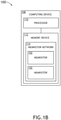
- the system 100 may include at least one device (e.g., at least one memristor 102) including at least two terminals 104, at least two conductive plates 105, and/or at least one memristor material 106. Some or all of the at least one memristor 102 and/or any other components of the system 100 may be communicatively coupled at any given time. Some embodiments may include multiple memristors 102 implemented as a memristor network 114 (as shown in FIGS. 1B-1D ).
- the memristor network 114 may include a plurality of at least partially communicatively coupled (e.g., at least partially interconnected) memristors 102 that may be arranged in an array, in parallel, and/or in series.
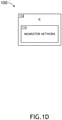
- the at least one memristor 102 may be fabricated on an integrated circuit (IC) device (e.g., IC 118, as shown in FIGS. 1C-1D ).
- the at least one memristor 102 may be part of a memory device (e.g., 112, as shown in FIG. 1B ).
- a first conductive plate 105 may be configured at least to receive an input signal via a first terminal 104; and a second conductive plate 105 may be configured at least to output an output signal via a second terminal 104.
- the at least one memristor material 106 may be positioned between the first conductive plate 105 and the second conductive plate 105.
- the at least one memristor material 106 may be composed of any suitable memristor material, such as any suitable ionic-covalent metal compound.
- each of the at least one memristor material 106 may comprise at least one of: at least one metal oxide (e.g., TiO 2 , ZrO 2 , NiO, CuO, CoO, Fe 2 O 3 , MoO, VO 2 , and/or HfO 2 ), at least one metal sulfide, at least one metal selenide, at least one metal telluride, at least one metal nitride, at least one metal phosphite, and/or at least one metal arsenide.
- at least one metal oxide e.g., TiO 2 , ZrO 2 , NiO, CuO, CoO, Fe 2 O 3 , MoO, VO 2 , and/or HfO 2
- at least one metal sulfide at least one metal selenide, at least one metal telluride, at least
- Each memristor material 106 may have oxygen vacancy and/or anion vacancy characteristics.
- Oxygen vacancy refers to a point defect in a crystal or glass where an oxygen ion is missing at an expected lattice or structure position, which results in a net positive charge, a trapped electron, and a metastable atomic structure.
- Anion vacancy refers to a point defect in a crystal or glass where an anion ion is missing at an expected lattice or structure position, which results in a net positive charge, a trapped electron, and a metastable atomic structure.
- the system 100 may include at least one computing device 108. If the system 100 includes multiple computing devices 108, some or all of the computing devices 108 may be communicatively coupled at any given time.
- the computing device 108 may include at least one processor 110 and/or at least one memory device 112, some or all of which may be communicatively coupled at any given time.
- each of the processor 110 and/or the memory device 112 may include at least one circuit (e.g., at least one IC 118, as shown in FIGS. 1C-1D ).
- the at least one processor 110 may be implemented as any suitable type and number of processors.
- the at least one processor 110 may include at least one general purpose processor (e.g., at least one central processing unit (CPU)), at least one digital signal processor (DSP), at least one application specific integrated circuit (ASIC), at least one field-programmable gate array (FPGA), at least one complex programmable logic device (CPLD), and/or at least one graphics processing unit (GPU).
- the at least one processor 110 may be configured to perform (e.g., collectively perform if more than one processor) any or all of the operations disclosed throughout.
- the processor 110 may be configured to run various software and/or firmware applications and/or computer code stored (e.g., maintained) in a non-transitory computer-readable medium (e.g., memory device 112) and configured to execute various instructions or operations.
- the at least one processor 110 may be configured to: output a signal; receive a signal; output data to the memory device 112; receive data from the memory device 112; determine and/or use a signature of a received signal; perform anti-piracy operations based at least on the signature; perform cyber security authentication operations based at least on the signature; perform unique data storage operations based at least on the signature; perform usage temperature authentication operations based at least on the signature; cause a barrier material to be fused; and/or cause an activation of at least one of a blocking material, a permanent modification material, or a transfer rate modification material.
- the memory device 112 may include the at least one memristor 102, which may be implemented as the memristor network 114 if more than one memristor 102.
- the memory device 112 may be a non-volatile and/or persistent memory device.
- the memory device 112 may be configured to: store data; read data; write data; output data; receive data; receive input signals; output signals; determine and/or use a signature of a received signal; perform anti-piracy operations based at least on the signature; perform cyber security authentication operations based at least on the signature; perform unique data storage operations based at least on the signature; perform usage temperature authentication operations based at least on the signature; cause a barrier material to be fused; and/or cause an activation of at least one of a blocking material, a permanent modification material, or a transfer rate modification material
- the system 100 may include at least one RF tuning device 116. If the system 100 includes multiple RF tuning devices 116, some or all of the RF tuning devices 116 may be communicatively coupled at any given time.
- the RF tuning device 116 may include at least one processor 110, at least one IC 118, and/or at least one memory device 112, some or all of which may be communicatively coupled at any given time.
- each of the processor 110, the IC 118, and/or the memory device 112 may include at least one circuit (e.g., at least one IC 118, as shown in FIGS. 1C-1D ).
- the RF tuning device 116 may be configured to tune RF signal outputs.
- the at least one processor 110 may be implemented similarly and function similarly to the processor 110 shown in FIG 1B , except that the at least one processor 110 may be further configured to cause RF tuning operations to be performed.
- the IC 118 may include the at least one memristor 102, which may be implemented as the memristor network 114 if more than one memristor 102.
- the at least one IC 118 may be configured to perform (e.g., collectively perform if more than one IC) any or all of the operations disclosed throughout.
- the IC 118 may be configured to run various software and/or firmware applications and/or computer code stored (e.g., maintained) in a non-transitory computer-readable medium (e.g., memory device 112) and configured to execute various instructions or operations.
- the IC 118 may be configured to: output a signal; receive a signal; output data to the memory device 112; receive data from the memory device 112; determine and/or use a signature of a received signal; perform anti-piracy operations based at least on the signature; perform cyber security authentication operations based at least on the signature; perform unique data storage operations based at least on the signature; perform usage temperature authentication operations based at least on the signature; cause a barrier material to be fused; cause an activation of at least one of a blocking material, a permanent modification material, or a transfer rate modification material; and/or perform RF signal tuning operations.
- the system 100 may include at least one circuit (e.g., at least one IC 118). If the system 100 includes multiple ICs 118, some or all of the ICs 118 may be communicatively coupled at any given time.
- the at least one IC 118 may be implemented similarly and function similarly to the IC 118 shown in and described with respect to FIG. 1C .
- FIGS. 2-6 exemplary embodiments of the system 100 including at least one memristor 102 according to the inventive concepts disclosed herein are depicted.
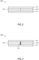
- FIG. 2 an exemplary embodiment of at least one memristor 102 according to the inventive concepts disclosed herein is depicted.
- the memristor 102 may include a first conductive plate 105 configured at least to receive an input signal, a second conductive plate 105 configured at least to output an output signal, and at least two memristor materials (e.g., a first memristor material 106-1 and a second memristor material 106-2).
- the first memristor material 106-1 may be positioned between the first conductive plate 105 and the second conductive plate 105.
- the second memristor material 106-2 may be positioned between the first conductive plate 105 and the second conductive plate 105.
- the first memristor material 106-1 and the second memristor material 106-2 may be in parallel electrically.
- the first memristor material 106-1 may be different from the second memristor material 106-2.
- the first memristor material 106-1 may be a relatively slower or faster response material than the second memristor material 106-2.
- Memristor response may depend on the crystal chemistry, crystal phase, the amount of underproportination and disproportionation, etc. Memristor response may be influenced by the cation-anion bond strength and the cation-anion size ratio.
- the responsiveness of the memristor materials 106 can be measured. In some embodiments, the responsiveness of the memristor materials 106 can be approximated by Gibbs Free Energy of Formation since Gibbs Free Energy of Formation incorporates several energy well/barrier type quantities.
- memristor materials 106 ordered from relatively slower approximated responsiveness to relatively faster approximated responsiveness are: Ti 2 O 3 at - 11,133,903 ⁇ Gf° (kJ/mol); Ta 2 O 5 at -1,910,984 ⁇ Gf° (kJ/mol); Sc 2 O 3 at -1,819,371 ⁇ Gf° (kJ/mol); Nb 2 O 5 at -1,765,859 ⁇ Gf° (kJ/mol); TiO 2 (Rutile) at -889,446 ⁇ Gf° (kJ/mol); TiO 2 (Anatase) at -883,303 ⁇ Gf° (kJ/mol); NbO 2 at -739,194 ⁇ Gf° (kJ/mol); MgO at -569,196 ⁇ Gf° (kJ/mol); and NbO at -391,945 ⁇ Gf° (kJ/mol).
- the first memristor 106-1 material has a first current-voltage (I-V) curve
- the second memristor material 106-2 has a second I-V curve
- the memristor 102 has a third I-V curve, wherein each of the first, second, and third I-V curves are different.
- the third I-V curve is indicative of an asymmetric time-based response (e.g., a homogenous asymmetric time-based response).
- the output signal of the memristor 102 may have a signature based at least on the asymmetric time-based response.
- the signature may be at least semi-unique (e.g., unique, unique to a product, or unique to a manufacturer) and/or may be indicative of at least one of an identity or an authenticity of an electronic component or device.
- a circuit e.g., an IC 118
- the signature can be achieved by strategically selection of the at least two memristor materials (e.g., 106-1, 106-2), dimensions of the at least two memristor materials (e.g., 106-1, 106-2), and/or an arrangement of the at least two memristor materials (e.g., 106-1, 106-2).
- the signature may be used as an identification feature for part authentication.
- FIG. 3 an exemplary embodiment of at least one memristor 102 according to the inventive concepts disclosed herein is depicted.
- the memristor 102 may be implemented similarly and function similarly to the memristor of FIG. 2 , except that the memristor 102 of FIG. 3 may include at least one barrier material 302.
- the barrier material 302 may extend from the first conductive plate 105 to the second conductive plate 105.
- the barrier material 302 may be positioned between the first memristor material 106-1 and the second memristor material 106-2 such that the first memristor material 106-1 is not in contact with the second memristor material 106-2.
- the barrier material 302 may be a fuse configured to permanently configure the memristor 102, for example, that may be activated thermally.
- suitable barrier materials may include any noble metal (e.g., Au, Pt, Ag, Ir, Rh, Ru, Pd, and/or Os), highly covalently bonded material (e.g., carbon allotropes, silicon allotropes, Ge, Te, and/or Se, etc%), mostly elemental forms of nonmetals and metalloids which form solids at standard temperature and pressure (STP) for periodic table groups 14, 15, and 16, or some combination thereof.
- noble metal e.g., Au, Pt, Ag, Ir, Rh, Ru, Pd, and/or Os
- highly covalently bonded material e.g., carbon allotropes, silicon allotropes, Ge, Te, and/or Se, etc.
- STP standard temperature and pressure
- the first memristor 106-1 material has a first current-voltage (I-V) curve
- the second memristor material 106-2 has a second I-V curve
- the memristor 102 has a third I-V curve, wherein each of the first, second, and third I-V curves are different.
- the third I-V curve is indicative of an asymmetric time-based response (e.g., a compartmentalized asymmetric time-based response).
- the output signal of the memristor 102 may have a signature based at least on the asymmetric time-based response.
- the signature may be at least semi-unique (e.g., unique, unique to a product, or unique to a manufacturer) and/or may be indicative of at least one of an identity or an authenticity of an electronic component or device.
- a circuit e.g., an IC 118
- the signature can be achieved by strategic selection of the at least two memristor materials (e.g., 106-1, 106-2), dimensions of the at least two memristor materials (e.g., 106-1, 106-2), and/or an arrangement of the at least two memristor materials (e.g., 106-1, 106-2).
- the signature may be used as an identification feature for part authentication.
- FIG. 4 an exemplary embodiment of at least one memristor 102 according to the inventive concepts disclosed herein is depicted.
- the memristor 102 may be implemented similarly and function similarly to the memristor of FIG. 2 and/or 3, except that the memristor 102 of FIG. 4 may include at least two of the first memristor material 106-1, at least two of the second memristor material 106-2, and at least two barrier material 302.
- the first memristor material 106-1 sections, the second memristor material 106-2 sections, and barrier material 302 sections may be interspersed (e.g., in one dimension or two dimensions (e.g., in a two-dimensional array)).
- one or more of the barrier material 302 sections may be omitted.
- the memristor 102 may include more than one (e.g., two, three, four, or more) type of memristor material 106.
- the barrier material 302 may be used to permanently change the memristor 102.
- the barrier material 302 may be used to permanently change a phase of the memristor 102.
- the barrier material 302 may be used to permanently configure the memristor 102, for example, to set the memristor 102 to a known value.
- the barrier material 302 may be activated thermally and act as a fusing structure.
- different materials for the memristor materials 106-1, 106-2 and/or the barrier material(s) 302 may be used to control a speed of and an amount of oxygen depletion transfer.
- memristors 102 may be arranged in an array as a memristor network 114.
- the memristor network 114 e.g., which may be implemented in the RF tuning device 116 may be used for configuring test values (e.g., resistance values).
- the memristor network 114 may be used to tune a circuit (e.g., an IC 118, such as an ASIC) by trimming resistance values (e.g., by using test selects).
- the memristor network 114 may be used to tune a resistor-capacitor (RC) circuit delay.
- RC resistor-capacitor
- the memristor network 114 may be configured as multiple interconnected memristors 102 or as a single memristor 102 having multiple fuseable barrier materials 302. In some embodiments, one memristor 102 of the memristor network 114 may influence another memristor 102 of the memristor network 114, for example, based on a fusing of a barrier material 302.
- At least one memristor 102 having at least one barrier material 302 may be used in the memory device 112 (e.g., a non-volatile memory device).
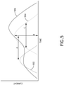
- the graph shows a first curve 502, a second curve 504, and a third curve 506.
- the first curve 502 demonstrates a responsiveness of the first memristor material 106-1.
- the second curve 504 demonstrates a responsiveness of the second memristor material 106-2.
- the third curve 506 demonstrates a responsiveness of the memristor 102 having the first memristor material 106-1 and the second memristor material 106-2.
- the third curve 506 may be indicative of an asymmetric time-based response (e.g., a homogenous asymmetric time-based response and/or a compartmentalized asymmetric time-based response) that may be associated with a signature as discussed herein.
- asymmetric time-based response e.g., a homogenous asymmetric time-based response and/or a compartmentalized asymmetric time-based response
- values of the output current for the memristor 102 can be read at various times (e.g., 5 times, as shown). The combination of the values read at different times can be used as a signature as discussed herein.
- Each memristor 102 may include at least one blocking material 602, at least one permanent modification material 902, and/or at least one transfer rate modification material 702.
- a blocking material 602 may be any suitable material that does not permit transmission of a memristor charge carrying mechanism.
- suitable blocking materials 602 include gold (Au), platinum (Pt), and/or palladium (Pd).
- a permanent modification material 902 may be any suitable material that absorbs memristor charge carriers.
- An example may be a cation oxidation number change that results in absorption or generation of total oxygen vacancies.
- suitable permanent modification materials 902 may include a metal oxide (e.g., a metal oxide near the surface of the electrode whose cation is reduced to its metallic form and whose anion fills the oxygen vacancy), such as a noble metal oxide.
- a transfer rate modification material 702 may be any suitable material that changes a transmission rate of memristor charge carriers.
- An example may be a transient or residual crystallographic phase change which results in a change in oxygen vacancy transmission rate.
- a transfer rate modification material 702 may be implemented by depositing a material in a metastable crystal phase or glassy phase (which may be inherently metastable) such that a thermal or optical stimulus initiates a phase shift to the more stable phase at the usage temperature. Depositing in a metastable phase can be accomplished by modifying the deposition rate, substrate biasing, and/or deposition pressure. Since the oxygen vacancy conduction rate is dependent on the crystal phase, the memristor response will be different after the phase transformation.
- TiO 2 in Rutile and Anatase may have a different memristor response since the bond strength is different and the crystal geometry is different.
- a transfer rate modification material 702 may be implemented by depositing a material that has a crystal phase transition over the operation temperature. In this embodiment the memristor response would change discontinuously at the temperature where the crystal phase changes.
- VO 2 has a monoclinic to tetragonal crystal phase transition around 67 degrees Celsius and may be a suitable transfer rate modification material 702.
- FIG. 7 an exemplary embodiment of at least one memristor 102 according to the inventive concepts disclosed herein is depicted.
- the memristor 102 may be implemented similarly and function similarly to the memristor 102 of FIG. 1A , except that the memristor 102 of FIG. 7 may include at least one transfer rate modification material 702.
- the transfer rate modification material 702 may be positioned between the first conductive plate 105 and the second conductive plate 105. At least a portion of the transfer rate modification material 702 may abut the memristor material 106. The transfer rate modification material 702 may provide a shift in a stabilization time to the output signal after a signal is driven from the second conductive plate 105 (B) to the first conductive plate 105 (A).
- the graph shows a first curve 802 and a second curve 804.
- the first curve 802 is associated with a baseline signal (e.g., an unmodified signal) before activation of the transfer rate modification material 702.
- the second curve 804 is associated with a modified signal after activation of the transfer rate modification material 702. For example, this modification may result in a modified output signal from the first conductive plate 105 (A) to the second conductive plate 105 (B).
- FIG. 9 an exemplary embodiment of at least one memristor 102 according to the inventive concepts disclosed herein is depicted.
- the memristor 102 may be implemented similarly and function similarly to the memristor 102 of FIG. 1A , except that the memristor 102 of FIG. 9 may include at least one permanent modification material 902.
- the permanent modification material 902 may be positioned between the first conductive plate 105 and the second conductive plate 105. At least a portion of the permanent modification material 902 may abut the memristor material 106.
- the permanent modification material 902 may provide a permanent signal modification (e.g., a permanent uniform signal modification) to the output signal after a signal is driven from the second conductive plate 105 (B) to the first conductive plate 105 (A). For example, this modification may result in a modified output signal from the first conductive plate 105 (A) to the second conductive plate 105 (B).
- Each subsequent activation e.g., by driving a signal from the second conductive plate 105 (B) to the first conductive plate 105 (A)
- Each subsequent activation e.g., by driving a signal from the second conductive plate 105 (B) to the first conductive plate 105 (A)
- each subsequent activation e.g., by driving a signal from the second conductive plate 105 (B) to
- the graph shows a first curve 1002 and a second curve 1004.
- the first curve 1002 is associated with a baseline signal (e.g., an unmodified signal) before activation of the permanent modification material 902.
- the second curve 1004 is associated with a modified signal after activation of the permanent modification material 902.
- the memristor 102 may be implemented similarly and function similarly to the memristor 102 of FIG. 9 , except that the at least one permanent modification material 902 does not fully extend along the first plate 105 (A).
- the memristor material 106 may abut a first surface area of the first conductive plate 105 (A).
- the memristor material 106 may abut a second surface area of the second conductive plate 105 (B).
- the first surface area and the second surface area may be different.
- the permanent signal modification may be a permanent asymmetric signal modification.
- the graph shows a first curve 1202, a second curve 1204, and a reduction slope 1206.
- the first curve 1202 is associated with a baseline signal (e.g., an unmodified signal) before activation of the permanent modification material 902.
- the second curve 1204 is associated with a modified signal after activation of the permanent modification material 902.
- the memristor 102 may be implemented similarly and function similarly to the memristor of FIG. 7 , except that the memristor 102 may be a notch filter.
- the device 102A may be implemented similarly and function similarly to the memristor 102 of FIG. 7 , except that the device 102A may further include at least one dielectric material 1402, a third conductive plate 105, and a third terminal 104.
- the device 102A may include the first conductive plate 105, the second conductive plate 105, the memristor material 106, a third conductive plate 105, a dielectric material 1402, a first terminal 104 electrically coupled to the first conductive plate 105, a second terminal 104 electrically coupled to the second conductive plate 105, and a third terminal 104 electrically coupled to the third conductive plate 105.
- the dielectric material 1402 may be positioned between the second conductive plate 105 and the third conductive plate 105.
- the device 102A may have memristor functionality and capacitor functionality.
- the device 102 may be a bandpass filter, which for example, may be combined RC time constant.
- FIGS. 15-16 exemplary embodiments of at least one memristor 102 according to the inventive concepts disclosed herein are depicted.
- the memristor 102 may be implemented similarly and function similarly to the memristor of FIG. 1A , except that in FIGS. 15-16 : the memristor material 106 may abut a first surface area of the first conductive plate 105 (A); the memristor material 106 may abut a second surface area of the second conductive plate 105 (B); and the first surface area and the second surface area may be different (e.g., the first surface area may be less the second surface area as shown in FIGS. 15-16 ).
- the 15-16 may provide an asymmetric signal response.
- the response can be modified to create greater oxygen vacancy density on the first conductive plate 105 (A) and lower density on the second conductive plate 105 (B).
- asymmetric application can be tailored by modification of a location and an amount of surface area covered by the blocking material 1602 (as shown in FIG. 16 ).
- the asymmetric response of the memristor 102 of FIGS. 15-16 can be used for: phase shifting an input signal (e.g., a digital clock phase shift); filtering by using only resistive elements; control system feedback; integrated analog compensation for undesired hysteresis effects (e.g., a lag in a temperature sensor reading versus actual instantaneous temperature) that can reduce or eliminate a need to compensate for such effects through software.
- phase shifting an input signal e.g., a digital clock phase shift
- filtering by using only resistive elements e.g., a digital clock phase shift
- control system feedback e.g., integrated analog compensation for undesired hysteresis effects (e.g., a lag in a temperature sensor reading versus actual instantaneous temperature) that can reduce or eliminate a need to compensate for such effects through software.
- opposing faces of the first and second conductive plates 105 may have different surface areas.
- the memristor 102 may further include a blocking material 1602.
- the blocking material 1602 may be positioned between the first conductive plate 105 and the second conductive plate 105.
- the blocking material 1602 may abut the memristor material 106 and one of the first conductive plate 105 or the second conductive plate 105.
- the graph shows a first I-V curve 1702 and a second I-V curve 1704.
- the first I-V curve 1702 is associated with a baseline signal (e.g., an unmodified signal) of a hypothetical memristor 102 with a first surface area of the first conductive plate 105 equal to the second surface area of the second conductive plate 105.
- the second I-V curve 1704 may be an I-V curve for the output signal of the memristor 102 of FIGS. 15-16 .
- FIG. 18 an exemplary embodiment of at least one memristor 102 according to the inventive concepts disclosed herein is depicted.
- the memristor 102 may be implemented similarly and function similarly to the memristor of FIG. 11 , except that in FIG.
- the memristor 102 includes a permanent modification material 902 and a transfer rate modification material 702; the permanent modification material 902 may be positioned between the first conductive plate 105 (A) and the second conductive plate 105 (B); the transfer rate modification material 702 may be positioned between the first conductive plate 105 (A) and the second conductive plate 105 (B); the permanent modification material 902 and the transfer rate modification material 702 may be in parallel electrically; at least a portion of the permanent modification material 902 may abut the memristor material 106; at least a portion of the transfer rate modification material 702 may abut the memristor material 106; a combination of the permanent modification material 902 and the transfer modification material 702 may provide a modification to the output signal after a signal is driven from the second conductive plate 105 (B) to the first conductive plate 105 (A).
- FIG. 19 an exemplary graph of current (I) versus voltage (V) is shown.
- the graph shows a first I-V curve 1902 and a second I-V curve 1904.
- the first I-V curve 1902 is associated with a baseline signal (e.g., an unmodified signal) of a memristor 102 as shown in FIG. 1A .
- the second I-V curve 1904 may be an I-V curve for the output signal of the memristor 102 of FIG. 18 .
- the system 100 may include a memristor network 114 having any combination of type and/or number of at least two memristors 102, such as shown in FIGS. 1A , 2 , 3 , 4 , 7 , 9 , 11 , 13 , 14 , 15, 16 , and/or 18.
- an exemplary embodiment of a method 2000 may include one or more of the following steps. Additionally, for example, some embodiments may include performing one more instances of the method 2000 iteratively, concurrently, and/or sequentially. Additionally, for example, at least some of the steps of the method 2000 may be performed in parallel and/or concurrently. Additionally, in some embodiments, at least some of the steps of the method 2000 may be performed non-sequentially. Additionally, in some embodiments, at least some of the steps of the method 2000 may be performed in sub-steps of providing various components. In some embodiments, the method 2000 may be performed by a semiconductor fab tool(s).
- a step 2002 may include providing a first conductive plate configured to receive an input signal.
- a step 2004 may include providing a second conductive plate configured to output an output signal.
- a step 2006 may include providing a first memristor material positioned between the first conductive plate and the second conductive plate.
- a step 2008 may include providing a second memristor material positioned between the first conductive plate and the second conductive plate, the first memristor material and the second memristor material being in parallel electrically, the first memristor material being different from the second memristor material.
- method 2000 may include any of the operations disclosed throughout.
- an exemplary embodiment of a method 2100 may include one or more of the following steps. Additionally, for example, some embodiments may include performing one more instances of the method 2100 iteratively, concurrently, and/or sequentially. Additionally, for example, at least some of the steps of the method 2100 may be performed in parallel and/or concurrently. Additionally, in some embodiments, at least some of the steps of the method 2100 may be performed non-sequentially. Additionally, in some embodiments, at least some of the steps of the method 2100 may be performed in sub-steps of providing various components. In some embodiments, the method 2100 may be performed by a semiconductor fab tool(s).
- a step 2102 may include providing a first conductive plate configured at least to receive an input signal.
- a step 2104 may include providing a second conductive plate configured at least to output an output signal.
- a step 2106 may include providing a memristor material positioned between the first conductive plate and the second conductive plate.
- method 2100 may include any of the operations disclosed throughout.
- embodiments of the inventive concepts disclosed herein may be directed to a method and a system including at least one device (e.g., at least one memristor) having at least one memristor material.
- at least one device e.g., at least one memristor
- At least one non-transitory computer-readable medium may refer to as at least one non-transitory computer-readable medium (e.g., at least one memory device (e.g., a non-volatile memory device); e.g., at least one memristor; e.g., at least one computer-readable medium implemented as hardware; e.g., at least one non-transitory processor-readable medium, at least one memory (e.g., at least one nonvolatile memory, at least one volatile memory, or a combination thereof; e.g., at least one random-access memory, at least one flash memory, at least one read-only memory (ROM) (e.g., at least one electrically erasable programmable read-only memory (EEPROM)), at least one on-processor memory (e.g., at least one on-processor cache, at least one on-processor buffer, at least one on-processor flash memory, at least one
- ROM read-only memory
- EEPROM electrically
- At least one means one or a plurality of; for example, “at least one” may comprise one, two, three, ..., one hundred, or more.
- one or more means one or a plurality of; for example, “one or more” may comprise one, two, three, ..., one hundred, or more.
- zero or more means zero, one, or a plurality of; for example, “zero or more” may comprise zero, one, two, three, ..., one hundred, or more.
- the methods, operations, and/or functionality disclosed may be implemented as sets of instructions or software readable by a device. Further, it is understood that the specific order or hierarchy of steps in the methods, operations, and/or functionality disclosed are examples of exemplary approaches. Based upon design preferences, it is understood that the specific order or hierarchy of steps in the methods, operations, and/or functionality can be rearranged while remaining within the scope of the inventive concepts disclosed herein.
- the accompanying claims may present elements of the various steps in a sample order, and are not necessarily meant to be limited to the specific order or hierarchy presented.
- embodiments of the methods according to the inventive concepts disclosed herein may include one or more of the steps described herein. Further, such steps may be carried out in any desired order and two or more of the steps may be carried out simultaneously with one another. Two or more of the steps disclosed herein may be combined in a single step, and in some embodiments, one or more of the steps may be carried out as two or more sub-steps. Further, other steps or sub-steps may be carried in addition to, or as substitutes to one or more of the steps disclosed herein.
- inventive concepts disclosed herein are well adapted to carry out the objects and to attain the advantages mentioned herein as well as those inherent in the inventive concepts disclosed herein. While presently preferred embodiments of the inventive concepts disclosed herein have been described for purposes of this disclosure, it will be understood that numerous changes may be made which will readily suggest themselves to those skilled in the art and which are accomplished within the broad scope and coverage of the inventive concepts disclosed and claimed herein.
Landscapes
- Engineering & Computer Science (AREA)
- Computer Security & Cryptography (AREA)
- Manufacturing & Machinery (AREA)
- Computer Networks & Wireless Communication (AREA)
- Signal Processing (AREA)
- Micromachines (AREA)
- Power Conversion In General (AREA)
Abstract
Description
- The present application is related to
United States Application Serial Number 17/017,313, titled SYSTEM AND DEVICE INCLUDING MEMRISTOR MATERIAL, filed September 10, 2020 . - Memristors have been the subject of discussion and research, but have not been used in many commercial applications.
- In one aspect, embodiments of the inventive concepts disclosed herein are directed to a system. The system may include a first conductive plate configured at least to receive an input signal and a second conductive plate configured at least to output an output signal. The system may further include a first memristor material positioned between the first conductive plate and the second conductive plate. The system may further include a second memristor material positioned between the first conductive plate and the second conductive plate. The first memristor material and the second memristor material may be in parallel electrically. The first memristor material may be different from the second memristor material.
- In a further aspect, embodiments of the inventive concepts disclosed herein are directed to a method. The method may include: providing a first conductive plate configured to receive an input signal; providing a second conductive plate configured to output an output signal; providing a first memristor material positioned between the first conductive plate and the second conductive plate; and/or providing a second memristor material positioned between the first conductive plate and the second conductive plate, the first memristor material and the second memristor material being in parallel electrically, the first memristor material being different from the second memristor material.
- In one aspect, embodiments of the inventive concepts disclosed herein are directed to a system. The system may include a first conductive plate configured at least to receive an input signal. The system may include a second conductive plate configured at least to output an output signal. The system may further include a memristor material positioned between the first conductive plate and the second conductive plate.
- In a further aspect, embodiments of the inventive concepts disclosed herein are directed to a method. The method may include: providing a first conductive plate configured at least to receive an input signal; providing a second conductive plate configured at least to output an output signal; and/or providing a memristor material positioned between the first conductive plate and the second conductive plate.
- Implementations of the inventive concepts disclosed herein may be better understood when consideration is given to the following detailed description thereof. Such description makes reference to the included drawings, which are not necessarily to scale, and in which some features may be exaggerated and some features may be omitted or may be represented schematically in the interest of clarity. Like reference numerals in the drawings may represent and refer to the same or similar element, feature, or function. In the drawings:
-
FIG. 1A is a view of an exemplary embodiment of a system including a memristor according to the inventive concepts disclosed herein. -
FIG. 1B is a view of an exemplary embodiment of the system ofFIG. 1A including a memristor according to the inventive concepts disclosed herein. -
FIG. 1C is a view of an exemplary embodiment of the system ofFIG. 1A including a memristor according to the inventive concepts disclosed herein. -
FIG. 1D is a view of an exemplary embodiment of the system ofFIG. 1A including a memristor according to the inventive concepts disclosed herein. -
FIG. 2 is an exemplary embodiment of a memristor according to the inventive concepts disclosed herein. -
FIG. 3 is an exemplary embodiment of a memristor according to the inventive concepts disclosed herein. -
FIG. 4 is an exemplary embodiment of a memristor according to the inventive concepts disclosed herein. -
FIG. 5 is an exemplary graph according to the inventive concepts disclosed herein. -
FIG. 6 is an exemplary graph according to the inventive concepts disclosed herein. -
FIG. 7 is an exemplary embodiment of a memristor according to the inventive concepts disclosed herein. -
FIG. 8 is an exemplary graph according to the inventive concepts disclosed herein. -
FIG. 9 is an exemplary embodiment of a memristor according to the inventive concepts disclosed herein. -
FIG. 10 is an exemplary graph according to the inventive concepts disclosed herein. -
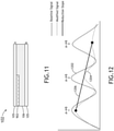
FIG. 11 is an exemplary embodiment of a memristor according to the inventive concepts disclosed herein. -
FIG. 12 is an exemplary graph according to the inventive concepts disclosed herein. -
FIG. 13 is an exemplary embodiment of a memristor according to the inventive concepts disclosed herein. -
FIG. 14 is an exemplary embodiment of a device according to the inventive concepts disclosed herein. -
FIG. 15 is an exemplary embodiment of a memristor according to the inventive concepts disclosed herein. -
FIG. 16 is an exemplary embodiment of a memristor according to the inventive concepts disclosed herein. -
FIG. 17 is an exemplary graph according to the inventive concepts disclosed herein. -
FIG. 18 is an exemplary embodiment of a memristor according to the inventive concepts disclosed herein. -
FIG. 19 is an exemplary graph according to the inventive concepts disclosed herein. -
FIG. 20 is a diagram of an exemplary embodiment of a method according to the inventive concepts disclosed herein. -
FIG. 21 is a diagram of an exemplary embodiment of a method according to the inventive concepts disclosed herein. - Before explaining at least one embodiment of the inventive concepts disclosed herein in detail, it is to be understood that the inventive concepts are not limited in their application to the details of construction and the arrangement of the components or steps or methodologies set forth in the following description or illustrated in the drawings. In the following detailed description of embodiments of the instant inventive concepts, numerous specific details are set forth in order to provide a more thorough understanding of the inventive concepts. However, it will be apparent to one of ordinary skill in the art having the benefit of the instant disclosure that the inventive concepts disclosed herein may be practiced without these specific details. In other instances, well-known features may not be described in detail to avoid unnecessarily complicating the instant disclosure. The inventive concepts disclosed herein are capable of other embodiments or of being practiced or carried out in various ways. Also, it is to be understood that the phraseology and terminology employed herein is for the purpose of description and should not be regarded as limiting.
- As used herein a letter following a reference numeral is intended to reference an embodiment of the feature or element that may be similar, but not necessarily identical, to a previously described element or feature bearing the same reference numeral (e.g., 1, 1a, 1b). Such shorthand notations are used for purposes of convenience only, and should not be construed to limit the inventive concepts disclosed herein in any way unless expressly stated to the contrary.
- Further, unless expressly stated to the contrary, "or" refers to an inclusive or and not to an exclusive or. For example, a condition A or B is satisfied by anyone of the following: A is true (or present) and B is false (or not present), A is false (or not present) and B is true (or present), and both A and B are true (or present).
- In addition, use of the "a" or "an" are employed to describe elements and components of embodiments of the instant inventive concepts. This is done merely for convenience and to give a general sense of the inventive concepts, and "a" and "an" are intended to include one or at least one and the singular also includes the plural unless it is obvious that it is meant otherwise.
- Finally, as used herein any reference to "one embodiment," or "some embodiments" means that a particular element, feature, structure, or characteristic described in connection with the embodiment is included in at least one embodiment of the inventive concepts disclosed herein. The appearances of the phrase "in some embodiments" in various places in the specification are not necessarily all referring to the same embodiment, and embodiments of the inventive concepts disclosed may include one or more of the features expressly described or inherently present herein, or any combination of sub-combination of two or more such features, along with any other features which may not necessarily be expressly described or inherently present in the instant disclosure.
- Broadly, embodiments of the inventive concepts disclosed herein are directed to a method and a system including at least one device (e.g., at least one memristor) having at least one memristor material.
- In some embodiments, for a memristor element, a desired signal response can be achieved by using (e.g., modifying) at least one particular material (e.g., at least one memristor material) as a transmission medium. In some embodiments, the signal response of the memristor can be modified by controlling an oxygen vacancy transmission rate of the at least one particular material. For example, controlling the oxygen vacancy transmission rate of the at least one particular material can be achieved by a physical modification and/or a chemical modification. In some embodiments, the signal response can provide an asymmetric time based response (e.g., a homogenous asymmetric time based response and/or a compartmentalized asymmetric time based response).
- Some embodiments may allow memristor characteristics to be tuned (e.g., tuned in real time during operation) to meet system design needs. Some embodiments may allow memristor elements to be tuned (e.g., additively tuned) around application specific integrated circuit (ASIC) circuitry, sometimes referred to as trimming. Some embodiments may provide circuit modification (e.g., additive circuit modification) of a memristor to improve ASIC shortcomings. Some embodiments may include tuning (e.g., additively tuning) memristor components to address timing specific needs of signal lines (e.g., key signal lines). For example, some embodiments may allow for custom signal optimization to account for a build process of circuit variance.
- Some embodiments may include physically changing an order and configuration of memristor structures to develop features with unique electrical responses. For example, by controlling a geometry of a medium that is passing a signal, a movement and effect of oxygen vacancies can be controlled so as to modify a response temporarily or permanently. Such responses can inhibit an asymmetric response, a permanent penalty associated with drive direction, a time based response modification, and/or a combination thereof.
- Some embodiments may allow for a potential to provide an element of repeatable uniqueness for use in anti-counterfeiting of electronic devices. Some embodiments may facilitate a generation of behavior based response techniques. Some embodiments may be useful for applications that need unique but repeatable responses (e.g., a unique fingerprint). Some embodiments may provide authenticity validation through unique but repeatable electrical responses.
- Some embodiments may include at least one filter (e.g., a high pass filter and/or a low pass filter), which may include at least one memristor instead of a capacitor.
- Referring now to
FIGS. 1A ,1B ,1C , and1D , exemplary embodiments of asystem 100 according to the inventive concepts disclosed herein are depicted. Thesystem 100 may be implemented as any suitable system, such as at least one vehicle system (e.g., at least one aircraft, at least one watercraft, at least one submersible craft, at least one automobile, and/or at least one train), a communication system, an optical system, a computing device system, a multiple computing device system, a radiofrequency (RF) device system, and/or a multiple RF device system. - For example, as shown in
FIG. 1A , thesystem 100 may include at least one device (e.g., at least one memristor 102) including at least twoterminals 104, at least twoconductive plates 105, and/or at least onememristor material 106. Some or all of the at least onememristor 102 and/or any other components of thesystem 100 may be communicatively coupled at any given time. Some embodiments may includemultiple memristors 102 implemented as a memristor network 114 (as shown inFIGS. 1B-1D ). For example, thememristor network 114 may include a plurality of at least partially communicatively coupled (e.g., at least partially interconnected)memristors 102 that may be arranged in an array, in parallel, and/or in series. In some embodiments, the at least onememristor 102 may be fabricated on an integrated circuit (IC) device (e.g.,IC 118, as shown inFIGS. 1C-1D ). In some embodiments, the at least onememristor 102 may be part of a memory device (e.g., 112, as shown inFIG. 1B ). - For example, a first
conductive plate 105 may be configured at least to receive an input signal via afirst terminal 104; and a secondconductive plate 105 may be configured at least to output an output signal via asecond terminal 104. For example, the at least onememristor material 106 may be positioned between the firstconductive plate 105 and the secondconductive plate 105. - In some embodiments, the at least one
memristor material 106 may be composed of any suitable memristor material, such as any suitable ionic-covalent metal compound. For example, each of the at least onememristor material 106 may comprise at least one of: at least one metal oxide (e.g., TiO2, ZrO2, NiO, CuO, CoO, Fe2O3, MoO, VO2, and/or HfO2), at least one metal sulfide, at least one metal selenide, at least one metal telluride, at least one metal nitride, at least one metal phosphite, and/or at least one metal arsenide. TiO2, ZrO2, NiO, CuO, CoO, Fe2O3, MoO, VO2, and HfO2 are known in the art to be suitable memristor materials. Eachmemristor material 106 may have oxygen vacancy and/or anion vacancy characteristics. Oxygen vacancy refers to a point defect in a crystal or glass where an oxygen ion is missing at an expected lattice or structure position, which results in a net positive charge, a trapped electron, and a metastable atomic structure. Anion vacancy refers to a point defect in a crystal or glass where an anion ion is missing at an expected lattice or structure position, which results in a net positive charge, a trapped electron, and a metastable atomic structure. - For example, as shown in
FIG. 1B , thesystem 100 may include at least onecomputing device 108. If thesystem 100 includesmultiple computing devices 108, some or all of thecomputing devices 108 may be communicatively coupled at any given time. - In some embodiments, the
computing device 108 may include at least oneprocessor 110 and/or at least onememory device 112, some or all of which may be communicatively coupled at any given time. In some embodiments, each of theprocessor 110 and/or thememory device 112 may include at least one circuit (e.g., at least oneIC 118, as shown inFIGS. 1C-1D ). - The at least one
processor 110 may be implemented as any suitable type and number of processors. For example, the at least oneprocessor 110 may include at least one general purpose processor (e.g., at least one central processing unit (CPU)), at least one digital signal processor (DSP), at least one application specific integrated circuit (ASIC), at least one field-programmable gate array (FPGA), at least one complex programmable logic device (CPLD), and/or at least one graphics processing unit (GPU). The at least oneprocessor 110 may be configured to perform (e.g., collectively perform if more than one processor) any or all of the operations disclosed throughout. Theprocessor 110 may be configured to run various software and/or firmware applications and/or computer code stored (e.g., maintained) in a non-transitory computer-readable medium (e.g., memory device 112) and configured to execute various instructions or operations. For example, the at least oneprocessor 110 may be configured to: output a signal; receive a signal; output data to thememory device 112; receive data from thememory device 112; determine and/or use a signature of a received signal; perform anti-piracy operations based at least on the signature; perform cyber security authentication operations based at least on the signature; perform unique data storage operations based at least on the signature; perform usage temperature authentication operations based at least on the signature; cause a barrier material to be fused; and/or cause an activation of at least one of a blocking material, a permanent modification material, or a transfer rate modification material. - The
memory device 112 may include the at least onememristor 102, which may be implemented as thememristor network 114 if more than onememristor 102. For example, thememory device 112 may be a non-volatile and/or persistent memory device. For example, thememory device 112 may be configured to: store data; read data; write data; output data; receive data; receive input signals; output signals; determine and/or use a signature of a received signal; perform anti-piracy operations based at least on the signature; perform cyber security authentication operations based at least on the signature; perform unique data storage operations based at least on the signature; perform usage temperature authentication operations based at least on the signature; cause a barrier material to be fused; and/or cause an activation of at least one of a blocking material, a permanent modification material, or a transfer rate modification material - For example, as shown in
FIG. 1C , thesystem 100 may include at least oneRF tuning device 116. If thesystem 100 includes multipleRF tuning devices 116, some or all of theRF tuning devices 116 may be communicatively coupled at any given time. - In some embodiments, the
RF tuning device 116 may include at least oneprocessor 110, at least oneIC 118, and/or at least onememory device 112, some or all of which may be communicatively coupled at any given time. In some embodiments, each of theprocessor 110, theIC 118, and/or thememory device 112 may include at least one circuit (e.g., at least oneIC 118, as shown inFIGS. 1C-1D ). TheRF tuning device 116 may be configured to tune RF signal outputs. - The at least one
processor 110 may be implemented similarly and function similarly to theprocessor 110 shown inFIG 1B , except that the at least oneprocessor 110 may be further configured to cause RF tuning operations to be performed. - The
IC 118 may include the at least onememristor 102, which may be implemented as thememristor network 114 if more than onememristor 102. The at least oneIC 118 may be configured to perform (e.g., collectively perform if more than one IC) any or all of the operations disclosed throughout. TheIC 118 may be configured to run various software and/or firmware applications and/or computer code stored (e.g., maintained) in a non-transitory computer-readable medium (e.g., memory device 112) and configured to execute various instructions or operations. For example, theIC 118 may be configured to: output a signal; receive a signal; output data to thememory device 112; receive data from thememory device 112; determine and/or use a signature of a received signal; perform anti-piracy operations based at least on the signature; perform cyber security authentication operations based at least on the signature; perform unique data storage operations based at least on the signature; perform usage temperature authentication operations based at least on the signature; cause a barrier material to be fused; cause an activation of at least one of a blocking material, a permanent modification material, or a transfer rate modification material; and/or perform RF signal tuning operations. - For example, as shown in
FIG. 1D , thesystem 100 may include at least one circuit (e.g., at least one IC 118). If thesystem 100 includesmultiple ICs 118, some or all of theICs 118 may be communicatively coupled at any given time. The at least oneIC 118 may be implemented similarly and function similarly to theIC 118 shown in and described with respect toFIG. 1C . - Referring now to
FIGS. 2-6 , exemplary embodiments of thesystem 100 including at least onememristor 102 according to the inventive concepts disclosed herein are depicted. - Referring now to
FIG. 2 , an exemplary embodiment of at least onememristor 102 according to the inventive concepts disclosed herein is depicted. - For example, the
memristor 102 may include a firstconductive plate 105 configured at least to receive an input signal, a secondconductive plate 105 configured at least to output an output signal, and at least two memristor materials (e.g., a first memristor material 106-1 and a second memristor material 106-2). The first memristor material 106-1 may be positioned between the firstconductive plate 105 and the secondconductive plate 105. The second memristor material 106-2 may be positioned between the firstconductive plate 105 and the secondconductive plate 105. The first memristor material 106-1 and the second memristor material 106-2 may be in parallel electrically. The first memristor material 106-1 may be different from the second memristor material 106-2. For example, the first memristor material 106-1 may be a relatively slower or faster response material than the second memristor material 106-2. Memristor response may depend on the crystal chemistry, crystal phase, the amount of underproportination and disproportionation, etc. Memristor response may be influenced by the cation-anion bond strength and the cation-anion size ratio. The responsiveness of thememristor materials 106 can be measured. In some embodiments, the responsiveness of thememristor materials 106 can be approximated by Gibbs Free Energy of Formation since Gibbs Free Energy of Formation incorporates several energy well/barrier type quantities. Based on approximated responsiveness using Gibbs Free Energy of Formation, some examples ofmemristor materials 106 ordered from relatively slower approximated responsiveness to relatively faster approximated responsiveness are: Ti2O3 at - 11,133,903 ΔGf° (kJ/mol); Ta2O5 at -1,910,984 ΔGf° (kJ/mol); Sc2O3 at -1,819,371 ΔGf° (kJ/mol); Nb2O5 at -1,765,859 ΔGf° (kJ/mol); TiO2 (Rutile) at -889,446 ΔGf° (kJ/mol); TiO2 (Anatase) at -883,303 ΔGf° (kJ/mol); NbO2 at -739,194 ΔGf° (kJ/mol); MgO at -569,196 ΔGf° (kJ/mol); and NbO at -391,945 ΔGf° (kJ/mol). - In some embodiments, the first memristor 106-1 material has a first current-voltage (I-V) curve, the second memristor material 106-2 has a second I-V curve, and the
memristor 102 has a third I-V curve, wherein each of the first, second, and third I-V curves are different. For example, as shown inFIG. 2 , the third I-V curve is indicative of an asymmetric time-based response (e.g., a homogenous asymmetric time-based response). In some embodiments, the output signal of the memristor 102 may have a signature based at least on the asymmetric time-based response. For example, the signature may be at least semi-unique (e.g., unique, unique to a product, or unique to a manufacturer) and/or may be indicative of at least one of an identity or an authenticity of an electronic component or device. In some embodiments a circuit (e.g., an IC 118) may be configured to receive and use the signature of the output signal for at least one of: anti-piracy, cyber security authentication, unique data storage, electronic serialization, or usage temperature authentication (e.g., by fusing the barrier material 302). For example, the signature can be achieved by strategically selection of the at least two memristor materials (e.g., 106-1, 106-2), dimensions of the at least two memristor materials (e.g., 106-1, 106-2), and/or an arrangement of the at least two memristor materials (e.g., 106-1, 106-2). For example, the signature may be used as an identification feature for part authentication. - Referring now to
FIG. 3 , an exemplary embodiment of at least onememristor 102 according to the inventive concepts disclosed herein is depicted. - For example, the
memristor 102 may be implemented similarly and function similarly to the memristor ofFIG. 2 , except that thememristor 102 ofFIG. 3 may include at least onebarrier material 302. - For example, the
barrier material 302 may extend from the firstconductive plate 105 to the secondconductive plate 105. Thebarrier material 302 may be positioned between the first memristor material 106-1 and the second memristor material 106-2 such that the first memristor material 106-1 is not in contact with the second memristor material 106-2. In some embodiments, thebarrier material 302 may be a fuse configured to permanently configure thememristor 102, for example, that may be activated thermally. For example, some embodiments of suitable barrier materials may include any noble metal (e.g., Au, Pt, Ag, Ir, Rh, Ru, Pd, and/or Os), highly covalently bonded material (e.g., carbon allotropes, silicon allotropes, Ge, Te, and/or Se, etc...), mostly elemental forms of nonmetals and metalloids which form solids at standard temperature and pressure (STP) for periodic table groups 14, 15, and 16, or some combination thereof. - In some embodiments, the first memristor 106-1 material has a first current-voltage (I-V) curve, the second memristor material 106-2 has a second I-V curve, and the
memristor 102 has a third I-V curve, wherein each of the first, second, and third I-V curves are different. For example, as shown inFIG. 2 , the third I-V curve is indicative of an asymmetric time-based response (e.g., a compartmentalized asymmetric time-based response). In some embodiments, the output signal of the memristor 102 may have a signature based at least on the asymmetric time-based response. For example, the signature may be at least semi-unique (e.g., unique, unique to a product, or unique to a manufacturer) and/or may be indicative of at least one of an identity or an authenticity of an electronic component or device. In some embodiments, a circuit (e.g., an IC 118) may be configured to receive and use the signature of the output signal for at least one of: anti-piracy, cyber security authentication, unique data storage, electronic serialization, or usage temperature authentication (e.g., by fusing the barrier material 302). For example, the signature can be achieved by strategic selection of the at least two memristor materials (e.g., 106-1, 106-2), dimensions of the at least two memristor materials (e.g., 106-1, 106-2), and/or an arrangement of the at least two memristor materials (e.g., 106-1, 106-2). For example, the signature may be used as an identification feature for part authentication. - Referring now to
FIG. 4 , an exemplary embodiment of at least onememristor 102 according to the inventive concepts disclosed herein is depicted. - For example, the
memristor 102 may be implemented similarly and function similarly to the memristor ofFIG. 2 and/or 3, except that thememristor 102 ofFIG. 4 may include at least two of the first memristor material 106-1, at least two of the second memristor material 106-2, and at least twobarrier material 302. For example, the first memristor material 106-1 sections, the second memristor material 106-2 sections, andbarrier material 302 sections may be interspersed (e.g., in one dimension or two dimensions (e.g., in a two-dimensional array)). In some embodiments, one or more of thebarrier material 302 sections may be omitted. In some embodiments, thememristor 102 may include more than one (e.g., two, three, four, or more) type ofmemristor material 106. - Referring to
FIGS. 3-4 , in some embodiments, thebarrier material 302 may be used to permanently change thememristor 102. For example, thebarrier material 302 may be used to permanently change a phase of thememristor 102. - For example, the
barrier material 302 may be used to permanently configure thememristor 102, for example, to set thememristor 102 to a known value. For example, thebarrier material 302 may be activated thermally and act as a fusing structure. In some embodiments, different materials for the memristor materials 106-1, 106-2 and/or the barrier material(s) 302 may be used to control a speed of and an amount of oxygen depletion transfer. - In some embodiments,
memristors 102 may be arranged in an array as amemristor network 114. For example, the memristor network 114 (e.g., which may be implemented in the RF tuning device 116) may be used for configuring test values (e.g., resistance values). For example, thememristor network 114 may be used to tune a circuit (e.g., anIC 118, such as an ASIC) by trimming resistance values (e.g., by using test selects). For example, thememristor network 114 may be used to tune a resistor-capacitor (RC) circuit delay. For example, such tuning may be similar to how mixed signals circuits are tuned by swapping resistors after a characterization test is complete, then retesting for proper performance. In some embodiments, thememristor network 114 may be configured as multipleinterconnected memristors 102 or as asingle memristor 102 having multiplefuseable barrier materials 302. In some embodiments, onememristor 102 of thememristor network 114 may influence anothermemristor 102 of thememristor network 114, for example, based on a fusing of abarrier material 302. - In some embodiments, at least one
memristor 102 having at least onebarrier material 302 may be used in the memory device 112 (e.g., a non-volatile memory device). - Referring now to
FIG. 5 , an exemplary graph of current versus time is shown. The graph shows afirst curve 502, asecond curve 504, and athird curve 506. Thefirst curve 502 demonstrates a responsiveness of the first memristor material 106-1. Thesecond curve 504 demonstrates a responsiveness of the second memristor material 106-2. Thethird curve 506 demonstrates a responsiveness of the memristor 102 having the first memristor material 106-1 and the second memristor material 106-2. Thethird curve 506 may be indicative of an asymmetric time-based response (e.g., a homogenous asymmetric time-based response and/or a compartmentalized asymmetric time-based response) that may be associated with a signature as discussed herein. - Referring now to
FIG. 6 , an exemplary graph of current versus time for amemristor 102 is shown. For example, values of the output current for the memristor 102 can be read at various times (e.g., 5 times, as shown). The combination of the values read at different times can be used as a signature as discussed herein. - Referring now to
FIGS. 7-19 , exemplary embodiments of thesystem 100 including at least onememristor 102 according to the inventive concepts disclosed herein are depicted. Eachmemristor 102 may include at least one blocking material 602, at least onepermanent modification material 902, and/or at least one transferrate modification material 702. - In some embodiments, a blocking material 602 may be any suitable material that does not permit transmission of a memristor charge carrying mechanism. Some examples of suitable blocking materials 602 include gold (Au), platinum (Pt), and/or palladium (Pd).
- In some embodiments, a
permanent modification material 902 may be any suitable material that absorbs memristor charge carriers. An example may be a cation oxidation number change that results in absorption or generation of total oxygen vacancies. Some examples of suitablepermanent modification materials 902 may include a metal oxide (e.g., a metal oxide near the surface of the electrode whose cation is reduced to its metallic form and whose anion fills the oxygen vacancy), such as a noble metal oxide. - In some embodiments, a transfer
rate modification material 702 may be any suitable material that changes a transmission rate of memristor charge carriers. An example may be a transient or residual crystallographic phase change which results in a change in oxygen vacancy transmission rate. For example, a transferrate modification material 702 may be implemented by depositing a material in a metastable crystal phase or glassy phase (which may be inherently metastable) such that a thermal or optical stimulus initiates a phase shift to the more stable phase at the usage temperature. Depositing in a metastable phase can be accomplished by modifying the deposition rate, substrate biasing, and/or deposition pressure. Since the oxygen vacancy conduction rate is dependent on the crystal phase, the memristor response will be different after the phase transformation. In some embodiments, for such an example, TiO2 in Rutile and Anatase may have a different memristor response since the bond strength is different and the crystal geometry is different. Additionally, for example, a transferrate modification material 702 may be implemented by depositing a material that has a crystal phase transition over the operation temperature. In this embodiment the memristor response would change discontinuously at the temperature where the crystal phase changes. For example, VO2 has a monoclinic to tetragonal crystal phase transition around 67 degrees Celsius and may be a suitable transferrate modification material 702. - Referring now to
FIG. 7 , an exemplary embodiment of at least onememristor 102 according to the inventive concepts disclosed herein is depicted. The memristor 102 may be implemented similarly and function similarly to thememristor 102 ofFIG. 1A , except that thememristor 102 ofFIG. 7 may include at least one transferrate modification material 702. - In some embodiments, the transfer
rate modification material 702 may be positioned between the firstconductive plate 105 and the secondconductive plate 105. At least a portion of the transferrate modification material 702 may abut thememristor material 106. The transferrate modification material 702 may provide a shift in a stabilization time to the output signal after a signal is driven from the second conductive plate 105 (B) to the first conductive plate 105 (A). - Referring now to
FIG. 8 , an exemplary graph of current versus time is shown. The graph shows afirst curve 802 and asecond curve 804. Thefirst curve 802 is associated with a baseline signal (e.g., an unmodified signal) before activation of the transferrate modification material 702. Thesecond curve 804 is associated with a modified signal after activation of the transferrate modification material 702. For example, this modification may result in a modified output signal from the first conductive plate 105 (A) to the second conductive plate 105 (B). - Referring now to
FIG. 9 , an exemplary embodiment of at least onememristor 102 according to the inventive concepts disclosed herein is depicted. The memristor 102 may be implemented similarly and function similarly to thememristor 102 ofFIG. 1A , except that thememristor 102 ofFIG. 9 may include at least onepermanent modification material 902. - In some embodiments, the
permanent modification material 902 may be positioned between the firstconductive plate 105 and the secondconductive plate 105. At least a portion of thepermanent modification material 902 may abut thememristor material 106. Thepermanent modification material 902 may provide a permanent signal modification (e.g., a permanent uniform signal modification) to the output signal after a signal is driven from the second conductive plate 105 (B) to the first conductive plate 105 (A). For example, this modification may result in a modified output signal from the first conductive plate 105 (A) to the second conductive plate 105 (B). Each subsequent activation (e.g., by driving a signal from the second conductive plate 105 (B) to the first conductive plate 105 (A)) of thepermanent modification material 902 may compound modification effects. - Referring now to
FIG. 10 , an exemplary graph of current versus time is shown. The graph shows afirst curve 1002 and asecond curve 1004. Thefirst curve 1002 is associated with a baseline signal (e.g., an unmodified signal) before activation of thepermanent modification material 902. Thesecond curve 1004 is associated with a modified signal after activation of thepermanent modification material 902. - Referring now to
FIG. 11 , an exemplary embodiment of at least onememristor 102 according to the inventive concepts disclosed herein is depicted. The memristor 102 may be implemented similarly and function similarly to thememristor 102 ofFIG. 9 , except that the at least onepermanent modification material 902 does not fully extend along the first plate 105 (A). For example, thememristor material 106 may abut a first surface area of the first conductive plate 105 (A). Thememristor material 106 may abut a second surface area of the second conductive plate 105 (B). The first surface area and the second surface area may be different. The permanent signal modification may be a permanent asymmetric signal modification. - Referring now to
FIG. 12 , an exemplary graph of current versus time is shown. The graph shows afirst curve 1202, asecond curve 1204, and areduction slope 1206. Thefirst curve 1202 is associated with a baseline signal (e.g., an unmodified signal) before activation of thepermanent modification material 902. Thesecond curve 1204 is associated with a modified signal after activation of thepermanent modification material 902. - Referring now to
FIG. 13 , an exemplary embodiment of at least onememristor 102 according to the inventive concepts disclosed herein is depicted. The memristor 102 may be implemented similarly and function similarly to the memristor ofFIG. 7 , except that the memristor 102 may be a notch filter. - Referring now to
FIG. 14 , an exemplary embodiment of at least onedevice 102A according to the inventive concepts disclosed herein is depicted. Thedevice 102A may be implemented similarly and function similarly to thememristor 102 ofFIG. 7 , except that thedevice 102A may further include at least onedielectric material 1402, a thirdconductive plate 105, and athird terminal 104. - The
device 102A may include the firstconductive plate 105, the secondconductive plate 105, thememristor material 106, a thirdconductive plate 105, adielectric material 1402, afirst terminal 104 electrically coupled to the firstconductive plate 105, asecond terminal 104 electrically coupled to the secondconductive plate 105, and athird terminal 104 electrically coupled to the thirdconductive plate 105. Thedielectric material 1402 may be positioned between the secondconductive plate 105 and the thirdconductive plate 105. Thedevice 102A may have memristor functionality and capacitor functionality. Thedevice 102 may be a bandpass filter, which for example, may be combined RC time constant. - Referring now to
FIGS. 15-16 , exemplary embodiments of at least onememristor 102 according to the inventive concepts disclosed herein are depicted. The memristor 102 may be implemented similarly and function similarly to the memristor ofFIG. 1A , except that inFIGS. 15-16 : thememristor material 106 may abut a first surface area of the first conductive plate 105 (A); thememristor material 106 may abut a second surface area of the second conductive plate 105 (B); and the first surface area and the second surface area may be different (e.g., the first surface area may be less the second surface area as shown inFIGS. 15-16 ). In some embodiments, the memristor ofFIGS. 15-16 may provide an asymmetric signal response. For example, the response can be modified to create greater oxygen vacancy density on the first conductive plate 105 (A) and lower density on the second conductive plate 105 (B). For example, such asymmetric application can be tailored by modification of a location and an amount of surface area covered by the blocking material 1602 (as shown inFIG. 16 ). - In some embodiments, the asymmetric response of the
memristor 102 ofFIGS. 15-16 can be used for: phase shifting an input signal (e.g., a digital clock phase shift); filtering by using only resistive elements; control system feedback; integrated analog compensation for undesired hysteresis effects (e.g., a lag in a temperature sensor reading versus actual instantaneous temperature) that can reduce or eliminate a need to compensate for such effects through software. - As shown in
FIG. 15 , opposing faces of the first and secondconductive plates 105 may have different surface areas. - As shown in
FIG. 16 , thememristor 102 may further include a blockingmaterial 1602. The blockingmaterial 1602 may be positioned between the firstconductive plate 105 and the secondconductive plate 105. The blockingmaterial 1602 may abut thememristor material 106 and one of the firstconductive plate 105 or the secondconductive plate 105. - Referring now to
FIG. 17 , an exemplary graph of current (I) versus voltage (V) is shown. The graph shows afirst I-V curve 1702 and asecond I-V curve 1704. Thefirst I-V curve 1702 is associated with a baseline signal (e.g., an unmodified signal) of ahypothetical memristor 102 with a first surface area of the firstconductive plate 105 equal to the second surface area of the secondconductive plate 105. Thesecond I-V curve 1704 may be an I-V curve for the output signal of thememristor 102 ofFIGS. 15-16 . - Referring now to
FIG. 18 , an exemplary embodiment of at least onememristor 102 according to the inventive concepts disclosed herein is depicted. The memristor 102 may be implemented similarly and function similarly to the memristor ofFIG. 11 , except that inFIG. 18 : thememristor 102 includes apermanent modification material 902 and a transferrate modification material 702; thepermanent modification material 902 may be positioned between the first conductive plate 105 (A) and the second conductive plate 105 (B); the transferrate modification material 702 may be positioned between the first conductive plate 105 (A) and the second conductive plate 105 (B); thepermanent modification material 902 and the transferrate modification material 702 may be in parallel electrically; at least a portion of thepermanent modification material 902 may abut thememristor material 106; at least a portion of the transferrate modification material 702 may abut thememristor material 106; a combination of thepermanent modification material 902 and thetransfer modification material 702 may provide a modification to the output signal after a signal is driven from the second conductive plate 105 (B) to the first conductive plate 105 (A). - Referring now to
FIG. 19 , an exemplary graph of current (I) versus voltage (V) is shown. The graph shows afirst I-V curve 1902 and asecond I-V curve 1904. Thefirst I-V curve 1902 is associated with a baseline signal (e.g., an unmodified signal) of a memristor 102 as shown inFIG. 1A . Thesecond I-V curve 1904 may be an I-V curve for the output signal of thememristor 102 ofFIG. 18 . - In some embodiments, the
system 100 may include amemristor network 114 having any combination of type and/or number of at least twomemristors 102, such as shown inFIGS. 1A ,2 ,3 ,4 ,7 ,9 ,11 ,13 ,14 ,15, 16 , and/or 18. - Referring now to
FIG. 20 , an exemplary embodiment of amethod 2000 according to the inventive concepts disclosed herein may include one or more of the following steps. Additionally, for example, some embodiments may include performing one more instances of themethod 2000 iteratively, concurrently, and/or sequentially. Additionally, for example, at least some of the steps of themethod 2000 may be performed in parallel and/or concurrently. Additionally, in some embodiments, at least some of the steps of themethod 2000 may be performed non-sequentially. Additionally, in some embodiments, at least some of the steps of themethod 2000 may be performed in sub-steps of providing various components. In some embodiments, themethod 2000 may be performed by a semiconductor fab tool(s). - A
step 2002 may include providing a first conductive plate configured to receive an input signal. - A
step 2004 may include providing a second conductive plate configured to output an output signal. - A
step 2006 may include providing a first memristor material positioned between the first conductive plate and the second conductive plate. - A
step 2008 may include providing a second memristor material positioned between the first conductive plate and the second conductive plate, the first memristor material and the second memristor material being in parallel electrically, the first memristor material being different from the second memristor material. - Further, the
method 2000 may include any of the operations disclosed throughout. - Referring now to
FIG. 21 , an exemplary embodiment of amethod 2100 according to the inventive concepts disclosed herein may include one or more of the following steps. Additionally, for example, some embodiments may include performing one more instances of themethod 2100 iteratively, concurrently, and/or sequentially. Additionally, for example, at least some of the steps of themethod 2100 may be performed in parallel and/or concurrently. Additionally, in some embodiments, at least some of the steps of themethod 2100 may be performed non-sequentially. Additionally, in some embodiments, at least some of the steps of themethod 2100 may be performed in sub-steps of providing various components. In some embodiments, themethod 2100 may be performed by a semiconductor fab tool(s). - A
step 2102 may include providing a first conductive plate configured at least to receive an input signal. - A
step 2104 may include providing a second conductive plate configured at least to output an output signal. - A
step 2106 may include providing a memristor material positioned between the first conductive plate and the second conductive plate. - Further, the
method 2100 may include any of the operations disclosed throughout. - As will be appreciated from the above, embodiments of the inventive concepts disclosed herein may be directed to a method and a system including at least one device (e.g., at least one memristor) having at least one memristor material.
- As used throughout and as would be appreciated by those skilled in the art, "at least one non-transitory computer-readable medium" may refer to as at least one non-transitory computer-readable medium (e.g., at least one memory device (e.g., a non-volatile memory device); e.g., at least one memristor; e.g., at least one computer-readable medium implemented as hardware; e.g., at least one non-transitory processor-readable medium, at least one memory (e.g., at least one nonvolatile memory, at least one volatile memory, or a combination thereof; e.g., at least one random-access memory, at least one flash memory, at least one read-only memory (ROM) (e.g., at least one electrically erasable programmable read-only memory (EEPROM)), at least one on-processor memory (e.g., at least one on-processor cache, at least one on-processor buffer, at least one on-processor flash memory, at least one on-processor EEPROM, or a combination thereof), or a combination thereof), at least one storage device (e.g., at least one hard-disk drive, at least one tape drive, at least one solid-state drive, at least one flash drive, at least one readable and/or writable disk of at least one optical drive configured to read from and/or write to the at least one readable and/or writable disk, or a combination thereof), or a combination thereof).
- As used throughout, "at least one" means one or a plurality of; for example, "at least one" may comprise one, two, three, ..., one hundred, or more. Similarly, as used throughout, "one or more" means one or a plurality of; for example, "one or more" may comprise one, two, three, ..., one hundred, or more. Further, as used throughout, "zero or more" means zero, one, or a plurality of; for example, "zero or more" may comprise zero, one, two, three, ..., one hundred, or more.
- In the present disclosure, the methods, operations, and/or functionality disclosed may be implemented as sets of instructions or software readable by a device. Further, it is understood that the specific order or hierarchy of steps in the methods, operations, and/or functionality disclosed are examples of exemplary approaches. Based upon design preferences, it is understood that the specific order or hierarchy of steps in the methods, operations, and/or functionality can be rearranged while remaining within the scope of the inventive concepts disclosed herein. The accompanying claims may present elements of the various steps in a sample order, and are not necessarily meant to be limited to the specific order or hierarchy presented.
- It is to be understood that embodiments of the methods according to the inventive concepts disclosed herein may include one or more of the steps described herein. Further, such steps may be carried out in any desired order and two or more of the steps may be carried out simultaneously with one another. Two or more of the steps disclosed herein may be combined in a single step, and in some embodiments, one or more of the steps may be carried out as two or more sub-steps. Further, other steps or sub-steps may be carried in addition to, or as substitutes to one or more of the steps disclosed herein.
- From the above description, it is clear that the inventive concepts disclosed herein are well adapted to carry out the objects and to attain the advantages mentioned herein as well as those inherent in the inventive concepts disclosed herein. While presently preferred embodiments of the inventive concepts disclosed herein have been described for purposes of this disclosure, it will be understood that numerous changes may be made which will readily suggest themselves to those skilled in the art and which are accomplished within the broad scope and coverage of the inventive concepts disclosed and claimed herein.
Claims (15)
- A system (100), comprising:a first conductive plate (105) configured at least to receive an input signal;a second conductive plate (105) configured at least to output an output signal;a first memristor material (106-1) positioned between the first conductive plate and the second conductive plate; anda second memristor material (106-2) positioned between the first conductive plate and the second conductive plate, the first memristor material and the second memristor material being in parallel electrically, the first memristor material being different from the second memristor material.
- The system of claim 1, further comprising a memristor (102), the memristor comprising the first conductive plate, the second conductive plate, the first memristor material, and the second memristor.
- The system of claim 2, further comprising an integrated circuit (118) "IC", the IC comprising the memristor.
- The system of claim 3, wherein the IC (118) is at least one of a non-volatile memory device or a radio frequency (RF) tuning device.
- The system of claim 2, wherein the first memristor material has a first current-voltage (I-V) curve, wherein the second memristor material has a second I-V curve, wherein the memristor has a third I-V curve, wherein each of the first, second, and third I-V curves is different.
- The system of claim 5, wherein the third I-V curve is indicative of an asymmetric time-based response.
- The system of claim 6, wherein the asymmetric time-based response is a homogenous asymmetric time-based response.
- The system of claim 6, wherein the asymmetric time-based response is a compartmentalized asymmetric time-based response.
- The system of claim 6, wherein the output signal has a signature based at least on the asymmetric time-based response.
- The system of claim 9, wherein the signature of the output signal is indicative of at least one of an identity or an authenticity of an electronic component.
- The system of claim 9, further comprising a circuit configured to use the signature of the output signal for at least one of: anti-piracy, cyber security authentication, unique data storage, or usage temperature authentication.
- The system of claim 2, wherein the memristor further comprises a barrier material, the barrier material extending from the first conductive plate to the second conductive plate, the barrier material positioned between the first memristor material and the second memristor material such that the first memristor material is not in contact with the second memristor material.
- The system of claim 12, wherein the barrier material is a fuse configured to permanently configure the memristor.
- The system of claim 13, wherein the fuse is activated thermally.
- A method (2000), comprising:Providing (2002) a first conductive plate configured to receive an input signal;providing (2004) a second conductive plate configured to output an output signal;providing (2006) a first memristor material positioned between the first conductive plate and the second conductive plate; andproviding (2008) a second memristor material positioned between the first conductive plate and the second conductive plate, the first memristor material and the second memristor material being in parallel electrically, the first memristor material being different from the second memristor material.
Applications Claiming Priority (1)
| Application Number | Priority Date | Filing Date | Title |
|---|---|---|---|
| US17/017,365 US11456418B2 (en) | 2020-09-10 | 2020-09-10 | System and device including memristor materials in parallel |
Publications (2)
| Publication Number | Publication Date |
|---|---|
| EP3968398A2 true EP3968398A2 (en) | 2022-03-16 |
| EP3968398A3 EP3968398A3 (en) | 2022-05-18 |
Family
ID=77666269
Family Applications (1)
| Application Number | Title | Priority Date | Filing Date |
|---|---|---|---|
| EP21195359.1A Pending EP3968398A3 (en) | 2020-09-10 | 2021-09-07 | System and device including memristor material |
Country Status (2)
| Country | Link |
|---|---|
| US (1) | US11456418B2 (en) |
| EP (1) | EP3968398A3 (en) |
Family Cites Families (53)
| Publication number | Priority date | Publication date | Assignee | Title |
|---|---|---|---|---|
| KR100773537B1 (en) | 2003-06-03 | 2007-11-07 | 삼성전자주식회사 | Non-volatile memory device including one switching element and one resistor, and manufacturing method thereof |
| KR101210548B1 (en) | 2008-11-27 | 2012-12-10 | 이화여자대학교 산학협력단 | A nanoparticle assembly-based switching device and a method for preparation of the same |
| US8471234B2 (en) | 2009-01-20 | 2013-06-25 | Hewlett-Packard Development Company, L.P. | Multilayer memristive devices |
| US8520425B2 (en) | 2010-06-18 | 2013-08-27 | Sandisk 3D Llc | Resistive random access memory with low current operation |
| US8385101B2 (en) | 2010-07-30 | 2013-02-26 | Hewlett-Packard Development Company, L.P. | Memory resistor having plural different active materials |
| EP2612357A4 (en) | 2010-08-30 | 2015-03-04 | Hewlett Packard Development Co | MULTILAYER MEMORY MATRIX |
| JP2012089567A (en) * | 2010-10-15 | 2012-05-10 | Toshiba Corp | Non-volatile resistance change element |
| US9432298B1 (en) | 2011-12-09 | 2016-08-30 | P4tents1, LLC | System, method, and computer program product for improving memory systems |
| US8711594B2 (en) | 2011-08-18 | 2014-04-29 | Hewlett-Packard Development Company, L.P. | Asymmetric switching rectifier |
| KR20130052371A (en) | 2011-11-11 | 2013-05-22 | 삼성전자주식회사 | Nonvolatile memory element and memory device including the same |
| CN102611408B (en) | 2012-04-09 | 2014-12-03 | 武汉科技大学 | Band-pass filter based on memristor |
| US9601195B2 (en) | 2013-07-31 | 2017-03-21 | Hewlett Packard Enterprise Development Lp | Voltage control for crosspoint memory structures |
| WO2015065337A1 (en) | 2013-10-29 | 2015-05-07 | Hewlett-Packard Development Company, L.P. | Resistive crosspoint memory array sensing |
| US9754666B2 (en) | 2014-01-31 | 2017-09-05 | Hewlett Packard Enterprise Development Lp | Resistive ratio-based memory cell |
| US9911495B2 (en) | 2014-01-31 | 2018-03-06 | Hewlett Packard Enterprise Development Lp | Memory cell having resistive and capacitive storage elements |
| US10026474B2 (en) | 2014-04-26 | 2018-07-17 | Hewlett Packard Enterprise Development Lp | Switched memristor analog tuning |
| US9911490B2 (en) | 2014-05-30 | 2018-03-06 | Hewlett Packard Enterprise Development Lp | Memory controllers |
| US10147762B2 (en) | 2014-06-26 | 2018-12-04 | Hewlett Packard Enterprise Development Lp | Protective elements for non-volatile memory cells in crossbar arrays |
| WO2016064375A1 (en) | 2014-10-20 | 2016-04-28 | Hewlett Packard Enterprise Development Lp | Clamp circuit |
| EP3210208B1 (en) | 2014-10-23 | 2022-11-30 | Hewlett-Packard Development Company, L.P. | Generating a representative logic indicator of grouped memristors |
| WO2016122523A1 (en) | 2015-01-29 | 2016-08-04 | Hewlett Packard Enterprise Development Lp | Resistive memory devices and arrays |
| US9735357B2 (en) | 2015-02-03 | 2017-08-15 | Crossbar, Inc. | Resistive memory cell with intrinsic current control |
| US10332595B2 (en) | 2015-02-24 | 2019-06-25 | Hewlett Packard Enterprise Development Lp | Determining resistance states of memristors in a crossbar array |
| US9583703B2 (en) | 2015-06-01 | 2017-02-28 | Boise State University | Tunable variable resistance memory device |
| EP3341940A1 (en) * | 2015-08-27 | 2018-07-04 | King Abdullah University Of Science And Technology | Read method compensating parasitic sneak currents in a crossbar memristive memory |
| CN105577355A (en) | 2015-12-12 | 2016-05-11 | 常州大学 | A voltage-controlled memristive chaotic circuit based on a second-order active bandpass filter |
| CN107623506A (en) | 2016-05-30 | 2018-01-23 | 王顺亭 | All-pass wave filtering circuit based on memristor |
| CN105957963B (en) | 2016-06-29 | 2018-09-21 | 北京印刷学院 | A kind of analogue type nano-wire array memristor and preparation method based on PET film |
| CN106301284B (en) | 2016-07-21 | 2018-07-13 | 华中科技大学 | A kind of adjustable filter circuit of bandwidth based on memristor and its operating method |
| WO2018112736A1 (en) | 2016-12-20 | 2018-06-28 | 北京大学 | Data search system and method |
| CN106487355A (en) | 2016-12-20 | 2017-03-08 | 滨州学院 | Single order high-pass filtering circuit based on memristor |
| CN106603220A (en) | 2016-12-22 | 2017-04-26 | 常州大学 | Three-order memristor active band-pass filter chaotic circuit |
| CN106788329A (en) | 2017-01-07 | 2017-05-31 | 滨州学院 | All-pass wave filtering circuit based on memristor |
| CN106712741A (en) | 2017-01-07 | 2017-05-24 | 滨州学院 | Band-pass filter circuit based on memristor |
| US9985206B1 (en) | 2017-02-01 | 2018-05-29 | International Business Machines Corporation | Resistive switching memory stack for three-dimensional structure |
| US10429343B1 (en) | 2017-02-09 | 2019-10-01 | National Technology & Engineering Solutions Of Sandia, Llc | Tunable ionic electronic transistor |
| US10504963B2 (en) * | 2017-08-30 | 2019-12-10 | Taiwan Semiconductor Manufacturing Co., Ltd. | RRAM memory cell with multiple filaments |
| US12183811B2 (en) | 2019-10-01 | 2024-12-31 | Northwestern University | Dual-gated memtransistor crossbar array, fabricating methods and applications of same |
| CN108365089A (en) | 2018-01-05 | 2018-08-03 | 中山大学 | Prepared by a kind of solution combustion method has analog- and digital- multi-functional NiO bases memory resistor and preparation method |
| US10454025B1 (en) * | 2018-06-13 | 2019-10-22 | International Business Machines Corporation | Phase change memory with gradual resistance change |
| WO2020018336A1 (en) | 2018-07-19 | 2020-01-23 | Northwestern University | Thermally activated memristors, fabricating methods and applications of same |
| DE102018213062B3 (en) | 2018-08-03 | 2019-11-14 | Fraunhofer-Gesellschaft zur Förderung der angewandten Forschung e.V. | Integrated electronic circuit comprising a first transistor and a ferroelectric capacitor and method for its production |
| US10930343B2 (en) | 2018-08-21 | 2021-02-23 | Hewlett Packard Enterprise Development Lp | Symmetric bipolar switching in memristors for artificial intelligence hardware |
| US11580411B2 (en) | 2018-12-18 | 2023-02-14 | Hewlett Packard Enterprise Development Lp | Systems for introducing memristor random telegraph noise in Hopfield neural networks |
| CN109743152A (en) | 2019-01-21 | 2019-05-10 | 江苏理工学院 | A kind of quadravalence memristor bandpass filter chaos circuit |
| JP7584899B2 (en) | 2019-06-17 | 2024-11-18 | 三星電子株式会社 | Memristor and neuromorphic device including same |
| US10804324B1 (en) | 2019-07-25 | 2020-10-13 | Tetramem Inc. | 1T2R RRAM cell and common reactive electrode in crossbar array circuits |
| KR102832728B1 (en) | 2019-10-28 | 2025-07-10 | 삼성전자주식회사 | Neuromorphic package devices and neuromorphic computing systems |
| US12373335B2 (en) | 2019-12-26 | 2025-07-29 | Intel Corporation | Memory thin provisioning using memory pools |
| US10810506B1 (en) | 2020-03-02 | 2020-10-20 | International Business Machines Corporation | Qubit biasing scheme using non-volatile devices |
| US11736305B2 (en) * | 2020-04-03 | 2023-08-22 | Arizona Board Of Regents On Behalf Of Northern Arizona University | Fast cryptographic key generation from memristor-based physical unclonable computed functions |
| CN115273932A (en) | 2020-04-06 | 2022-11-01 | 昕原半导体(上海)有限公司 | Unique chip identifier utilizing the unclonable nature of on-chip resistive memory arrays |
| KR102861762B1 (en) | 2020-05-22 | 2025-09-17 | 삼성전자주식회사 | Apparatus for performing in memory processing and computing apparatus having the same |
-
2020
- 2020-09-10 US US17/017,365 patent/US11456418B2/en active Active
-
2021
- 2021-09-07 EP EP21195359.1A patent/EP3968398A3/en active Pending
Also Published As
| Publication number | Publication date |
|---|---|
| US11456418B2 (en) | 2022-09-27 |
| US20220077390A1 (en) | 2022-03-10 |
| EP3968398A3 (en) | 2022-05-18 |
Similar Documents
| Publication | Publication Date | Title |
|---|---|---|
| Park et al. | Differences in nature of defects between SrBi 2 Ta 2 O 9 and Bi 4 Ti 3 O 12 | |
| US7796416B2 (en) | Variable resistance element, its manufacturing method and semiconductor memory device comprising the same | |
| PhilipáWong | Multi-level control of conductive nano-filament evolution in HfO 2 ReRAM by pulse-train operations | |
| US6473332B1 (en) | Electrically variable multi-state resistance computing | |
| US5278636A (en) | Non-volatile, solid state bistable electrical switch | |
| US11462267B2 (en) | System and device including memristor material | |
| Nan et al. | Voltage control of metal-insulator transition and non-volatile ferroelastic switching of resistance in VOx/PMN-PT heterostructures | |
| CN101295763B (en) | Resistive memory device and resistive random access memory stack structure | |
| US8212621B2 (en) | Memristive programmable frequency source and method | |
| JP4805865B2 (en) | Variable resistance element | |
| BRPI0719055A2 (en) | Correlated memory of electrons | |
| Kundozerova et al. | Anodic $\hbox {Nb} _ {2}\hbox {O} _ {5} $ Nonvolatile RRAM | |
| KR20040111563A (en) | Solid electrolyte switching device, fpga using same, memory device, and method for manufacturing solid electrolyte switching device | |
| Siannas et al. | Electronic synapses enabled by an epitaxial SrTiO3‐δ/Hf0. 5Zr0. 5O2 ferroelectric field‐effect memristor integrated on silicon | |
| EP2272113B1 (en) | Multiple bit phase change memory cell | |
| CN111133598A (en) | Scalable and low voltage, non-cast nanoscale vanadium dioxide threshold switching device and relaxation oscillator with current controlled negative differential resistance | |
| Funck et al. | Comprehensive model for the electronic transport in Pt/SrTi O 3 analog memristive devices | |
| JPWO2011052239A1 (en) | Resistance variable nonvolatile memory device and method of forming memory cell | |
| US11631808B2 (en) | System and device including memristor material | |
| US20100073823A1 (en) | Piezoelectric actuator, head slider and magnetic disk drive | |
| JP2014022660A (en) | Variable resistance element, and nonvolatile semiconductor memory device provided with variable resistance element | |
| Li et al. | Realization of resistive switching and magnetoresistance in ZnO/ZnO-Co composite materials | |
| Li et al. | Regulation of oxygen vacancy on behaviors of memristors based on amorphous ZnTiSnO films | |
| US20160351804A1 (en) | Tunable Variable Resistance Memory Device | |
| EP3968399B1 (en) | System and device including memristor material |
Legal Events
| Date | Code | Title | Description |
|---|---|---|---|
| PUAI | Public reference made under article 153(3) epc to a published international application that has entered the european phase |
Free format text: ORIGINAL CODE: 0009012 |
|
| STAA | Information on the status of an ep patent application or granted ep patent |
Free format text: STATUS: THE APPLICATION HAS BEEN PUBLISHED |
|
| AK | Designated contracting states |
Kind code of ref document: A2 Designated state(s): AL AT BE BG CH CY CZ DE DK EE ES FI FR GB GR HR HU IE IS IT LI LT LU LV MC MK MT NL NO PL PT RO RS SE SI SK SM TR |
|
| PUAL | Search report despatched |
Free format text: ORIGINAL CODE: 0009013 |
|
| AK | Designated contracting states |
Kind code of ref document: A3 Designated state(s): AL AT BE BG CH CY CZ DE DK EE ES FI FR GB GR HR HU IE IS IT LI LT LU LV MC MK MT NL NO PL PT RO RS SE SI SK SM TR |
|
| RIC1 | Information provided on ipc code assigned before grant |
Ipc: H01L 45/00 20060101AFI20220411BHEP |
|
| STAA | Information on the status of an ep patent application or granted ep patent |
Free format text: STATUS: REQUEST FOR EXAMINATION WAS MADE |
|
| 17P | Request for examination filed |
Effective date: 20221117 |
|
| RBV | Designated contracting states (corrected) |
Designated state(s): AL AT BE BG CH CY CZ DE DK EE ES FI FR GB GR HR HU IE IS IT LI LT LU LV MC MK MT NL NO PL PT RO RS SE SI SK SM TR |
|
| STAA | Information on the status of an ep patent application or granted ep patent |
Free format text: STATUS: EXAMINATION IS IN PROGRESS |
|
| 17Q | First examination report despatched |
Effective date: 20251017 |