EP3967652A1 - Layered compound and nanosheet containing indium and arsenic, and electrical device using the same - Google Patents
Layered compound and nanosheet containing indium and arsenic, and electrical device using the same Download PDFInfo
- Publication number
- EP3967652A1 EP3967652A1 EP20211720.6A EP20211720A EP3967652A1 EP 3967652 A1 EP3967652 A1 EP 3967652A1 EP 20211720 A EP20211720 A EP 20211720A EP 3967652 A1 EP3967652 A1 EP 3967652A1
- Authority
- EP
- European Patent Office
- Prior art keywords
- layered compound
- nanosheet
- layered
- compound according
- compound
- Prior art date
- Legal status (The legal status is an assumption and is not a legal conclusion. Google has not performed a legal analysis and makes no representation as to the accuracy of the status listed.)
- Pending
Links
Images






Classifications
-
- C—CHEMISTRY; METALLURGY
- C01—INORGANIC CHEMISTRY
- C01G—COMPOUNDS CONTAINING METALS NOT COVERED BY SUBCLASSES C01D OR C01F
- C01G15/00—Compounds of gallium, indium or thallium
- C01G15/006—Compounds containing gallium, indium or thallium, with or without oxygen or hydrogen, and containing two or more other elements
-
- B—PERFORMING OPERATIONS; TRANSPORTING
- B82—NANOTECHNOLOGY
- B82Y—SPECIFIC USES OR APPLICATIONS OF NANOSTRUCTURES; MEASUREMENT OR ANALYSIS OF NANOSTRUCTURES; MANUFACTURE OR TREATMENT OF NANOSTRUCTURES
- B82Y40/00—Manufacture or treatment of nanostructures
-
- C—CHEMISTRY; METALLURGY
- C01—INORGANIC CHEMISTRY
- C01G—COMPOUNDS CONTAINING METALS NOT COVERED BY SUBCLASSES C01D OR C01F
- C01G28/00—Compounds of arsenic
- C01G28/002—Compounds containing arsenic, with or without oxygen or hydrogen, and containing two or more other elements
-
- C—CHEMISTRY; METALLURGY
- C30—CRYSTAL GROWTH
- C30B—SINGLE-CRYSTAL GROWTH; UNIDIRECTIONAL SOLIDIFICATION OF EUTECTIC MATERIAL OR UNIDIRECTIONAL DEMIXING OF EUTECTOID MATERIAL; REFINING BY ZONE-MELTING OF MATERIAL; PRODUCTION OF A HOMOGENEOUS POLYCRYSTALLINE MATERIAL WITH DEFINED STRUCTURE; SINGLE CRYSTALS OR HOMOGENEOUS POLYCRYSTALLINE MATERIAL WITH DEFINED STRUCTURE; AFTER-TREATMENT OF SINGLE CRYSTALS OR A HOMOGENEOUS POLYCRYSTALLINE MATERIAL WITH DEFINED STRUCTURE; APPARATUS THEREFOR
- C30B29/00—Single crystals or homogeneous polycrystalline material with defined structure characterised by the material or by their shape
- C30B29/10—Inorganic compounds or compositions
- C30B29/40—AIIIBV compounds wherein A is B, Al, Ga, In or Tl and B is N, P, As, Sb or Bi
-
- C—CHEMISTRY; METALLURGY
- C30—CRYSTAL GROWTH
- C30B—SINGLE-CRYSTAL GROWTH; UNIDIRECTIONAL SOLIDIFICATION OF EUTECTIC MATERIAL OR UNIDIRECTIONAL DEMIXING OF EUTECTOID MATERIAL; REFINING BY ZONE-MELTING OF MATERIAL; PRODUCTION OF A HOMOGENEOUS POLYCRYSTALLINE MATERIAL WITH DEFINED STRUCTURE; SINGLE CRYSTALS OR HOMOGENEOUS POLYCRYSTALLINE MATERIAL WITH DEFINED STRUCTURE; AFTER-TREATMENT OF SINGLE CRYSTALS OR A HOMOGENEOUS POLYCRYSTALLINE MATERIAL WITH DEFINED STRUCTURE; APPARATUS THEREFOR
- C30B29/00—Single crystals or homogeneous polycrystalline material with defined structure characterised by the material or by their shape
- C30B29/60—Single crystals or homogeneous polycrystalline material with defined structure characterised by the material or by their shape characterised by shape
-
- C—CHEMISTRY; METALLURGY
- C30—CRYSTAL GROWTH
- C30B—SINGLE-CRYSTAL GROWTH; UNIDIRECTIONAL SOLIDIFICATION OF EUTECTIC MATERIAL OR UNIDIRECTIONAL DEMIXING OF EUTECTOID MATERIAL; REFINING BY ZONE-MELTING OF MATERIAL; PRODUCTION OF A HOMOGENEOUS POLYCRYSTALLINE MATERIAL WITH DEFINED STRUCTURE; SINGLE CRYSTALS OR HOMOGENEOUS POLYCRYSTALLINE MATERIAL WITH DEFINED STRUCTURE; AFTER-TREATMENT OF SINGLE CRYSTALS OR A HOMOGENEOUS POLYCRYSTALLINE MATERIAL WITH DEFINED STRUCTURE; APPARATUS THEREFOR
- C30B29/00—Single crystals or homogeneous polycrystalline material with defined structure characterised by the material or by their shape
- C30B29/60—Single crystals or homogeneous polycrystalline material with defined structure characterised by the material or by their shape characterised by shape
- C30B29/64—Flat crystals, e.g. plates, strips or discs
-
- C—CHEMISTRY; METALLURGY
- C30—CRYSTAL GROWTH
- C30B—SINGLE-CRYSTAL GROWTH; UNIDIRECTIONAL SOLIDIFICATION OF EUTECTIC MATERIAL OR UNIDIRECTIONAL DEMIXING OF EUTECTOID MATERIAL; REFINING BY ZONE-MELTING OF MATERIAL; PRODUCTION OF A HOMOGENEOUS POLYCRYSTALLINE MATERIAL WITH DEFINED STRUCTURE; SINGLE CRYSTALS OR HOMOGENEOUS POLYCRYSTALLINE MATERIAL WITH DEFINED STRUCTURE; AFTER-TREATMENT OF SINGLE CRYSTALS OR A HOMOGENEOUS POLYCRYSTALLINE MATERIAL WITH DEFINED STRUCTURE; APPARATUS THEREFOR
- C30B29/00—Single crystals or homogeneous polycrystalline material with defined structure characterised by the material or by their shape
- C30B29/60—Single crystals or homogeneous polycrystalline material with defined structure characterised by the material or by their shape characterised by shape
- C30B29/68—Crystals with laminate structure, e.g. "superlattices"
-
- C—CHEMISTRY; METALLURGY
- C30—CRYSTAL GROWTH
- C30B—SINGLE-CRYSTAL GROWTH; UNIDIRECTIONAL SOLIDIFICATION OF EUTECTIC MATERIAL OR UNIDIRECTIONAL DEMIXING OF EUTECTOID MATERIAL; REFINING BY ZONE-MELTING OF MATERIAL; PRODUCTION OF A HOMOGENEOUS POLYCRYSTALLINE MATERIAL WITH DEFINED STRUCTURE; SINGLE CRYSTALS OR HOMOGENEOUS POLYCRYSTALLINE MATERIAL WITH DEFINED STRUCTURE; AFTER-TREATMENT OF SINGLE CRYSTALS OR A HOMOGENEOUS POLYCRYSTALLINE MATERIAL WITH DEFINED STRUCTURE; APPARATUS THEREFOR
- C30B33/00—After-treatment of single crystals or homogeneous polycrystalline material with defined structure
- C30B33/06—Joining of crystals
-
- C—CHEMISTRY; METALLURGY
- C30—CRYSTAL GROWTH
- C30B—SINGLE-CRYSTAL GROWTH; UNIDIRECTIONAL SOLIDIFICATION OF EUTECTIC MATERIAL OR UNIDIRECTIONAL DEMIXING OF EUTECTOID MATERIAL; REFINING BY ZONE-MELTING OF MATERIAL; PRODUCTION OF A HOMOGENEOUS POLYCRYSTALLINE MATERIAL WITH DEFINED STRUCTURE; SINGLE CRYSTALS OR HOMOGENEOUS POLYCRYSTALLINE MATERIAL WITH DEFINED STRUCTURE; AFTER-TREATMENT OF SINGLE CRYSTALS OR A HOMOGENEOUS POLYCRYSTALLINE MATERIAL WITH DEFINED STRUCTURE; APPARATUS THEREFOR
- C30B33/00—After-treatment of single crystals or homogeneous polycrystalline material with defined structure
- C30B33/08—Etching
- C30B33/10—Etching in solutions or melts
-
- C—CHEMISTRY; METALLURGY
- C30—CRYSTAL GROWTH
- C30B—SINGLE-CRYSTAL GROWTH; UNIDIRECTIONAL SOLIDIFICATION OF EUTECTIC MATERIAL OR UNIDIRECTIONAL DEMIXING OF EUTECTOID MATERIAL; REFINING BY ZONE-MELTING OF MATERIAL; PRODUCTION OF A HOMOGENEOUS POLYCRYSTALLINE MATERIAL WITH DEFINED STRUCTURE; SINGLE CRYSTALS OR HOMOGENEOUS POLYCRYSTALLINE MATERIAL WITH DEFINED STRUCTURE; AFTER-TREATMENT OF SINGLE CRYSTALS OR A HOMOGENEOUS POLYCRYSTALLINE MATERIAL WITH DEFINED STRUCTURE; APPARATUS THEREFOR
- C30B9/00—Single-crystal growth from melt solutions using molten solvents
- C30B9/04—Single-crystal growth from melt solutions using molten solvents by cooling of the solution
- C30B9/06—Single-crystal growth from melt solutions using molten solvents by cooling of the solution using as solvent a component of the crystal composition
-
- H—ELECTRICITY
- H10—SEMICONDUCTOR DEVICES; ELECTRIC SOLID-STATE DEVICES NOT OTHERWISE PROVIDED FOR
- H10D—INORGANIC ELECTRIC SEMICONDUCTOR DEVICES
- H10D62/00—Semiconductor bodies, or regions thereof, of devices having potential barriers
- H10D62/10—Shapes, relative sizes or dispositions of the regions of the semiconductor bodies; Shapes of the semiconductor bodies
- H10D62/117—Shapes of semiconductor bodies
- H10D62/118—Nanostructure semiconductor bodies
-
- H—ELECTRICITY
- H10—SEMICONDUCTOR DEVICES; ELECTRIC SOLID-STATE DEVICES NOT OTHERWISE PROVIDED FOR
- H10N—ELECTRIC SOLID-STATE DEVICES NOT OTHERWISE PROVIDED FOR
- H10N70/00—Solid-state devices having no potential barriers, and specially adapted for rectifying, amplifying, oscillating or switching
- H10N70/801—Constructional details of multistable switching devices
- H10N70/881—Switching materials
- H10N70/884—Switching materials based on at least one element of group IIIA, IVA or VA, e.g. elemental or compound semiconductors
-
- H—ELECTRICITY
- H10—SEMICONDUCTOR DEVICES; ELECTRIC SOLID-STATE DEVICES NOT OTHERWISE PROVIDED FOR
- H10P—GENERIC PROCESSES OR APPARATUS FOR THE MANUFACTURE OR TREATMENT OF DEVICES COVERED BY CLASS H10
- H10P14/00—Formation of materials, e.g. in the shape of layers or pillars
- H10P14/20—Formation of materials, e.g. in the shape of layers or pillars of semiconductor materials
- H10P14/32—Formation of materials, e.g. in the shape of layers or pillars of semiconductor materials characterised by intermediate layers between substrates and deposited layers
- H10P14/3202—Materials thereof
- H10P14/3214—Materials thereof being Group IIIA-VA semiconductors
- H10P14/3221—Arsenides
-
- H—ELECTRICITY
- H10—SEMICONDUCTOR DEVICES; ELECTRIC SOLID-STATE DEVICES NOT OTHERWISE PROVIDED FOR
- H10P—GENERIC PROCESSES OR APPARATUS FOR THE MANUFACTURE OR TREATMENT OF DEVICES COVERED BY CLASS H10
- H10P14/00—Formation of materials, e.g. in the shape of layers or pillars
- H10P14/20—Formation of materials, e.g. in the shape of layers or pillars of semiconductor materials
- H10P14/32—Formation of materials, e.g. in the shape of layers or pillars of semiconductor materials characterised by intermediate layers between substrates and deposited layers
- H10P14/3242—Structure
- H10P14/3244—Layer structure
- H10P14/3246—Monolayers
-
- H—ELECTRICITY
- H10—SEMICONDUCTOR DEVICES; ELECTRIC SOLID-STATE DEVICES NOT OTHERWISE PROVIDED FOR
- H10P—GENERIC PROCESSES OR APPARATUS FOR THE MANUFACTURE OR TREATMENT OF DEVICES COVERED BY CLASS H10
- H10P14/00—Formation of materials, e.g. in the shape of layers or pillars
- H10P14/20—Formation of materials, e.g. in the shape of layers or pillars of semiconductor materials
- H10P14/34—Deposited materials, e.g. layers
- H10P14/3402—Deposited materials, e.g. layers characterised by the chemical composition
- H10P14/3414—Deposited materials, e.g. layers characterised by the chemical composition being group IIIA-VIA materials
- H10P14/3421—Arsenides
-
- B—PERFORMING OPERATIONS; TRANSPORTING
- B82—NANOTECHNOLOGY
- B82Y—SPECIFIC USES OR APPLICATIONS OF NANOSTRUCTURES; MEASUREMENT OR ANALYSIS OF NANOSTRUCTURES; MANUFACTURE OR TREATMENT OF NANOSTRUCTURES
- B82Y30/00—Nanotechnology for materials or surface science, e.g. nanocomposites
-
- C—CHEMISTRY; METALLURGY
- C01—INORGANIC CHEMISTRY
- C01P—INDEXING SCHEME RELATING TO STRUCTURAL AND PHYSICAL ASPECTS OF SOLID INORGANIC COMPOUNDS
- C01P2004/00—Particle morphology
- C01P2004/20—Particle morphology extending in two dimensions, e.g. plate-like
- C01P2004/24—Nanoplates, i.e. plate-like particles with a thickness from 1-100 nanometer
Definitions
- the present invention relates to a layered compound and a nanosheet containing indium and arsenic, and an electrical device using the same, and more particularly, to a layered compound and a nanosheet containing an alkali metal or alkaline earth metal and containing indium and arsenic having various electrical properties, and an electrical device using the same.
- Layered compounds connected to interlayers through van der Waals bonds may show various properties, and the layered compounds may be delaminated through physical or chemical methods to prepare two-dimensional (2D) nanosheets having a thickness of several to hundreds of nanometers, and thus, active research into the layered compounds is underway.
- 2D two-dimensional
- low-dimensional materials such as nanosheets are expected to have innovative new functions that existing bulk materials fail to provide, and are highly likely to serve as next-generation future materials instead of the existing materials.
- the layered compounds having a two-dimensional crystal structure are limited to materials such as graphite, transition metals, and chalcogen compounds to hardly develop into materials of various compositions.
- indium arsenide is widely used in high-power, high-frequency electrical devices as a compound semiconductor material but ternary indium arsenide having a layered structure is not specifically known till now.
- Ternary indium arsenide compounds having a layered structure unlike existing indium arsenide compounds having a different crystal structure, are expected to allow diversified application, and to be applicable to new areas that have not been reached before.
- a layered Group III-V compound having indium and arsenic having indium and arsenic, a nanosheet that may be prepared using the same, and an electrical device including the materials.
- a layered compound represented by [Formula 1] Na 1-x In y As z (0 ⁇ x ⁇ 1.0, 0.8 ⁇ y ⁇ 1.2, 1.2 ⁇ z ⁇ 1.8).
- a nanosheet including a compound represented by [Formula 1] Na 1-x In y As z (0 ⁇ x ⁇ 1.0, 0.8 ⁇ y ⁇ 12, 1.2 ⁇ z ⁇ 1.8), and prepared through a physical or chemical peeling method.
- an electrical device including the layered compound or nanosheet as described above.
- the electrical device may be a memristor.
- a layered compound and a nanosheet provided through an embodiment of the invention may have various electrical properties, thereby enabling the development of new electrical devices.
- the layered compound or nanosheet according to an embodiment of the invention may be represented by Formula 1 below.
- Formula 1 Na 1-x In y As z (0 ⁇ x ⁇ 1.0, 0.8 ⁇ y ⁇ 12, 1.2 ⁇ z ⁇ 1.8)
- InAs is a zinc blende crystal structure, which is incapable of having a layered structure, and accordingly, peeling InAs to form a nanosheet was hardly achievable.
- inventors of the invention have come up with an idea of adding additive elements to In y As z to place the additive elements between In y As z layers so as to prepare a layered compound in which the In y As z layers are connected.
- the inventors have calculated to create a layered material having a new composition and a crystal structure, and as a result, they have succeeded to synthesize a previously unreported new composition of a layered Na 2 In 2 As 3 so as to prepare a layered compound having a composition of Formula 1 above.
- Na is positioned between the In y As z layers to weakly bond the In y As z layers through van der Waals bonds, and a plane on which Na is positioned forms a cleavage plane that is easily cleaved along the plane.
- x may be 0 according to Formula 1 described above, and as described above, Na 2 In 2 As 3 is a previously unreported new synthesized material where x is 0 in Formula 1. Even without the removal of Na, the plane containing Na may be peeled off as a cleavage plane that forms weak van der Waals bonds.
- Na is positioned between the In y As z layers to weakly bond the In y As z layers through the van der Waals bonds, and along this cleavage plane, the plane may thus be easily peeled off into the In y As z layers through either or both physical or chemical methods, and the more Na is removed, the easier the peeling is. Accordingly, through a physical or chemical peeling method, an In y As z nanosheet may be easily obtained from the layered compound, and in this case, Na may partially remain in the In y As z nanosheet.
- the layered structure of the layered compound described in the invention includes a case where repeating two-dimensional In y As z layers are interlayer-bonded through van der Waals bonds by additive element Na as well as a case where the interlayer bonding force between In y As z layers is removed to increase the interlayer distance, thereby causing cracks.
- Na is removed to weaken the interlayer bond, and accordingly, easier peeling to prepare a nanosheet may be achievable.
- the nanosheet prepared through the peeling from the layered compound may be a single layer of In y As z , but may be formed when a plurality of layers overlaps to be several hundreds of nm thick.
- nanosheets may exhibit anisotropy according to a two-dimensional shape only when a thickness to a lateral width is less than a certain level.
- the ratio of a thickness (d) to a width (L) of a nanosheet (d/L) is preferably 0.1 or less.
- a width of the nanosheet prepared through an embodiment of the invention may be 5 ⁇ m or greater, and thus, a thickness of the nanosheet is preferably 500nm or less. In this case, Na may partially remain in the In y As z nanosheet.
- the nanosheet according to an embodiment of the invention refers to a sheet peeled off from a layered compound through a physical or chemical method, and includes being formed as a plurality of In y As z layers in addition to being formed as a single In y As z layer.
- FIG. 1 A conceptual view of examples of the layered compound and the nanosheet is shown in FIG. 1 , which shows that an additive element, Na 11, is positioned between In y As z layers 10 of NaIn y As z to keep the bond between the In y As z layers 10, and in this case, the removal of Na 11 allows the layers to switch to Na 1-x In y As z , and to weaken the bond between the In y As z layers 10, and thus to be easily peeled off physically or chemically, thereby, in the end, developing into a In y As z nanosheet 20. Nanosheets prepared using this way may still contain some Na 11.
- the crystal structure of the layered compound may have a space group of P2 1 /c.
- residual Na in the Na 1-x In y As z layered compound or nanosheet may be in the range of 0.3 ⁇ x ⁇ 0.8 according to Formula 1 below.
- the additive element is removed in a certain fraction or greater from the Na 1-x In y As z compound and the rest some remain. x for this may have a range of 0.3 ⁇ x ⁇ 0.8.
- y may satisfy 0.8 ⁇ y ⁇ 1.2, and z may satisfy 1.2 ⁇ z ⁇ 1.8, and y and z may have slight changes due to defects in initially prepared Na 2 In 2 As 3 , and the removal of Na may cause slight changes in the ratio of In to As during the removal process, and thus, values of y and z in Na 1-x In y As z may change within a range that does not alter the crystal structure for a given amount of Na.
- a strong acid such as nitric acid or hydrochloric acid may be used for the removal of additive elements, and as the additive elements are removed through the strong acid, the place where the additive elements are removed is replaced with hydrogen ions contained in the strong acid which is then bonded thereto, and thus a layered compound containing hydrogen and a nanosheet prepared using the compound may be provided.
- the layered compound containing hydrogen ions or the nanosheet therefrom may be represented by Formula 2 below.
- Formula 2 Na 1-x H n In y As z (0 ⁇ x ⁇ 1.0, 0.8 ⁇ y ⁇ 12, 1.2 ⁇ z ⁇ 1.8, 0 ⁇ n ⁇ x)
- hydrogen ions replace Na, an additive element, and are added in less than the amount of Na removed.
- the range of x an amount from which Na is removed, may be 0.1 ⁇ x ⁇ 0.9, and more preferably may be 0.3 ⁇ x ⁇ 0.8.
- the layered structure of the initial layered compound, NaIn y As z is kept as it is, and as the additive element, Na, is partially removed, the interlayer bonding force is weakened to easily peel the compound off into the In y As z layers, thereby exhibiting various electrical properties through the residual additive elements.
- n above may have the same value as x, and hydrogen ions may replace the removed additive elements to be contained in the layered structure compound.
- the layered compound and the nanosheet described above exhibit various properties as a result of analysis, and these properties will be described below.
- the layered compound and the nanosheet described above may have a space group of P2 1 /c in XRD measurement using CuK ⁇ rays.
- the layered compound has a I (102) /I (002) value of 0.40 or less which is a peak intensity of a (102) plane to a peak intensity of a (002) plane. This is caused when the interlayer distance gradually increases due to the removal of the additive elements from the layered compound, and the same is true for the nanosheet.
- the layered compound in which the additional element, Na partially remains, and the nanosheet using the compound may exhibit various electrical properties due to the residual Na.
- the layered compound or nanosheet as described above may exhibit various electrical properties due to a unique layered structure and residual additive elements.
- the layered structure compound or the nanosheet according to an embodiment of the invention exhibits ferroelectric-like properties.
- Ferroelectric properties are generally found in oxides of an asymmetric structure such as BaTiO 3 of a perovskite structure, and are found according to changes in the position of Ba located at the center.
- the layered structure compound or the nanosheet according to an embodiment of the invention does not have the asymmetric structure, but nevertheless exhibits ferroelectric properties.
- the layered structure compound or the nanosheet does not have an asymmetrical structure, the layered structure compound or the nanosheet still exhibit ferroelectric-like properties since the position of the residual additive elements moves according to an external electric field.
- ferroelectric-like properties of the layered compound or nanosheet according to an embodiment of the invention enables application to various electrical devices.
- the layered structure compound or the nanosheet according to an embodiment of the invention may exhibit resistance switching properties.
- resistance switching properties are generally found in oxides, and recently, using these properties, memory devices such as a memristor capable of storing information like a flash memory have been actively developed, and, through the resistance switching properties, the layered compound and the nanosheet of an embodiment of the invention may be actively used in the development of memory devices such as the memristor.
- Na, In, and As were weighed at a molar ratio of 2:2:3, mixed, and then put into an alumina crucible. Next, the mixture was placed in a quartz tube which was then double-sealed to block outside air. The process was performed in a glove box under argon atmosphere. Thereafter, the resultant was put at a temperature raised to 1000°C in a box furnace, kept for 12 hours, cooled to 500°C at a temperature reduction rate of 5 °C/h, then kept for 100 hours at 500°C, and cooled to room temperature to obtain Na 2 In 2 As 3 .
- the inventors have calculated to project a layered structure using vienna ab initio simulation package (VASP) for a previously unreported new Na 2 In 2 As 3 compound, and as a result, they have found out that the layered structure had a structure of P2 1 /c similar to known Na 2 Al 2 As 3 and Na 2 Ga 2 As 3 .
- VASP vienna ab initio simulation package
- FIG. 2 shows XRD diffraction patterns (Na 2 In 2 As 3 _vasp) of Na 2 In 2 As 3 projected through the calculation using VASP and XRD rotation patterns of Sample A(Na 2 In 2 As 3 _synthesis) synthesized through the method described above.
- Fig. 3 shows a scanning electron microscopy (SEM) image of the synthesized Sample A and results of energy dispersive spectroscopy (EDS) analysis. From the EDS results, it was found that the synthesized Sample A was composed of Na, In, and As.
- Fig. 4 shows results of transmission electron microscopy (TEM) analysis of Sample A.
- SAED selected area electron diffraction
- Fig. 5 shows a schematic view of the structure of Na 2 In 2 As 3 and results of scanning transmission electron microscopy (STEM) analysis.
- STEM scanning transmission electron microscopy
- Fig. 6 shows changes in XRD peaks according to the removal of Na.
- the interplanar distance of the (002) plane was 7.42 ⁇ , and as Na was removed, the interplanar distance gradually increased up to 7.47 ⁇ .
- Changes in the XRD peaks as well were observed according to the changes in the interplanar distance, and it was found that with the removal of Na, the size of the peaks of the (102) plane to the peaks of the (002) plane gradually decreased. Accordingly, the value of I (102) /I (002) was 0.46 in Sample A, decreased to 0.13 in Sample B and to 0.09 in Sample D.
- the (002) and (102) planes showed the same peaks, indicating that the crystal structure having a P2 1 /c space group was kept.
- FIG. 7 shows a nanosheet prepared by removing Na from Sample A to become Sample C, and being peeled off from Sample C using a tape.
- Sample A a cleavage plane between the layers was observed, but in Sample C, as Na was removed, the interlayer distance increased, thereby forming cracks.
- Fig. 8 shows an atomic force microscopy (AFM) image of a nanosheet prepared by being peeled off from Sample C and a line-profile therefrom. It was confirmed that a nanosheet was peeled off to have a thickness of 10 nm to 30 nm.
- AFM atomic force microscopy
- Fig. 9 shows results of scanning transmission electron microscopy (STEM) analysis of Sample D. The data showed that Na was partially removed and there were no changes in the crystal structure even after the removal.
- Fig. 10 is results of TEM analysis of Sample E. It was found that an amorphous structure appeared with the excessive removal of Na.
- the nanosheet kept a high resistance state 1, indicating a low current flow, but when the voltage was greater than a certain level, the nanosheet switched to a low resistance state 2, indicating a sharp increase in the current, and the same properties were shown in an opposite electrode direction, thereby showing resistance switching properties.
- the nanosheet would be applied as a memristor device, which is being actively developed as a neuromorphic memory device.
Landscapes
- Chemical & Material Sciences (AREA)
- Engineering & Computer Science (AREA)
- Organic Chemistry (AREA)
- Crystallography & Structural Chemistry (AREA)
- Materials Engineering (AREA)
- Metallurgy (AREA)
- Inorganic Chemistry (AREA)
- Nanotechnology (AREA)
- Physics & Mathematics (AREA)
- Condensed Matter Physics & Semiconductors (AREA)
- General Physics & Mathematics (AREA)
- Composite Materials (AREA)
- Manufacturing & Machinery (AREA)
- Inorganic Compounds Of Heavy Metals (AREA)
- Semiconductor Memories (AREA)
Abstract
Description
- The present invention relates to a layered compound and a nanosheet containing indium and arsenic, and an electrical device using the same, and more particularly, to a layered compound and a nanosheet containing an alkali metal or alkaline earth metal and containing indium and arsenic having various electrical properties, and an electrical device using the same.
- Layered compounds connected to interlayers through van der Waals bonds may show various properties, and the layered compounds may be delaminated through physical or chemical methods to prepare two-dimensional (2D) nanosheets having a thickness of several to hundreds of nanometers, and thus, active research into the layered compounds is underway.
- In particular, low-dimensional materials such as nanosheets are expected to have innovative new functions that existing bulk materials fail to provide, and are highly likely to serve as next-generation future materials instead of the existing materials.
- However, up until now, the layered compounds having a two-dimensional crystal structure are limited to materials such as graphite, transition metals, and chalcogen compounds to hardly develop into materials of various compositions.
- Meanwhile, indium arsenide is widely used in high-power, high-frequency electrical devices as a compound semiconductor material but ternary indium arsenide having a layered structure is not specifically known till now.
- Ternary indium arsenide compounds having a layered structure, unlike existing indium arsenide compounds having a different crystal structure, are expected to allow diversified application, and to be applicable to new areas that have not been reached before.
- According to an embodiment of the invention, there are provided a layered Group III-V compound having indium and arsenic, a nanosheet that may be prepared using the same, and an electrical device including the materials.
- According to an embodiment of the invention, there is provided a layered compound represented by [Formula 1] Na1-xInyAsz (0≤x<1.0, 0.8≤y≤1.2, 1.2≤z≤1.8).
- According to an embodiment of the invention, there is provided a nanosheet including a compound represented by [Formula 1] Na1-xInyAsz (0≤x<1.0, 0.8≤y≤12, 1.2≤z≤1.8), and prepared through a physical or chemical peeling method.
- According to an embodiment of the invention, there is provided an electrical device including the layered compound or nanosheet as described above.
- In addition, the electrical device may be a memristor.
- A layered compound and a nanosheet provided through an embodiment of the invention may have various electrical properties, thereby enabling the development of new electrical devices.
-
-
Fig. 1 is a conceptual diagram of a layered compound and a nanosheet prepared according to an embodiment of the invention; -
Fig. 2 is a graph showing XRD diffraction patterns of a layered compound according to an embodiment of the invention; -
Fig. 3 shows a scanning electron microscopy (SEM) image of a layered compound according to an embodiment of the invention and results of energy dispersive spectroscopy (EDS) analysis; -
Fig. 4 shows results of transmission electron microscopy (TEM) analysis of a layered compound according to an embodiment of the invention; -
Fig. 5 shows a schematic view of the structure of Na2In2As3 according to an embodiment of the invention and results of scanning transmission electron microscopy (STEM) analysis; -
Fig. 6 is shows results of XRD analysis of a layered compound according to an embodiment of the invention; -
Fig. 7 is SEM and TEM images of a layered compound and a nanosheet according to an embodiment of the invention; -
Fig. 8 shows an atomic force microscopy (AFM) image of a nanosheet according to an embodiment of the invention and a line-profile therefrom; -
Fig. 9 shows results of STEM analysis of a layered compound according to an embodiment of the invention; -
Fig. 10 shows results of TEM analysis of a layered compound according to an embodiment of the invention; -
Fig.11 shows results of evaluation on ferroelectric properties of a nanosheet according to an embodiment of the invention through piezoresponse force microscopy (PFM); and -
Fig. 12 is a graph of changes in current according to voltage for a nanosheet according to an embodiment of the invention. - Hereinafter, configuration and operation of embodiments of the invention will be described with reference to the accompanying drawings. In the following description, when it is determined that the specific description of the known related art unnecessarily obscures the gist of the invention, the detailed description thereof will be omitted. In addition, when an element "includes" a component, it may indicate that the element does not exclude another component unless explicitly described to the contrary, but can further include another component.
- The layered compound or nanosheet according to an embodiment of the invention may be represented by Formula 1 below.
[Formula 1] Na1-xInyAsz
(0≤x<1.0, 0.8≤y≤12, 1.2≤z≤1.8) - In general, InAs is a zinc blende crystal structure, which is incapable of having a layered structure, and accordingly, peeling InAs to form a nanosheet was hardly achievable.
- In order to overcome the limitation, inventors of the invention have come up with an idea of adding additive elements to InyAsz to place the additive elements between InyAsz layers so as to prepare a layered compound in which the InyAsz layers are connected. To this end, the inventors have calculated to create a layered material having a new composition and a crystal structure, and as a result, they have succeeded to synthesize a previously unreported new composition of a layered Na2In2As3 so as to prepare a layered compound having a composition of
Formula 1 above. - In the layered compound having the composition of
Formula 1, Na is positioned between the InyAsz layers to weakly bond the InyAsz layers through van der Waals bonds, and a plane on which Na is positioned forms a cleavage plane that is easily cleaved along the plane. - Meanwhile, in the composition of Na in the Na1-xInyAsz layered compound or nanosheet, x may be 0 according to Formula 1 described above, and as described above, Na2In2As3 is a previously unreported new synthesized material where x is 0 in Formula 1. Even without the removal of Na, the plane containing Na may be peeled off as a cleavage plane that forms weak van der Waals bonds.
- In the layered compound according to an embodiment of the invention, as described above, Na is positioned between the InyAsz layers to weakly bond the InyAsz layers through the van der Waals bonds, and along this cleavage plane, the plane may thus be easily peeled off into the InyAsz layers through either or both physical or chemical methods, and the more Na is removed, the easier the peeling is. Accordingly, through a physical or chemical peeling method, an InyAsz nanosheet may be easily obtained from the layered compound, and in this case, Na may partially remain in the InyAsz nanosheet.
- With the continuous removal of the additive element Na, the distance between the InyAsz compound layers gradually become greater to weaken the interlayer bond force, and eventually the bond between the layers breaks down, which may cause cracks between the layers. Therefore, the layered structure of the layered compound described in the invention includes a case where repeating two-dimensional InyAsz layers are interlayer-bonded through van der Waals bonds by additive element Na as well as a case where the interlayer bonding force between InyAsz layers is removed to increase the interlayer distance, thereby causing cracks. As such, Na is removed to weaken the interlayer bond, and accordingly, easier peeling to prepare a nanosheet may be achievable.
- The nanosheet prepared through the peeling from the layered compound may be a single layer of InyAsz, but may be formed when a plurality of layers overlaps to be several hundreds of nm thick. In general, nanosheets may exhibit anisotropy according to a two-dimensional shape only when a thickness to a lateral width is less than a certain level. To this end, the ratio of a thickness (d) to a width (L) of a nanosheet (d/L) is preferably 0.1 or less. A width of the nanosheet prepared through an embodiment of the invention may be 5 µm or greater, and thus, a thickness of the nanosheet is preferably 500nm or less. In this case, Na may partially remain in the InyAsz nanosheet.
- As such, the nanosheet according to an embodiment of the invention refers to a sheet peeled off from a layered compound through a physical or chemical method, and includes being formed as a plurality of InyAsz layers in addition to being formed as a single InyAsz layer.
- A conceptual view of examples of the layered compound and the nanosheet is shown in
FIG. 1 , which shows that an additive element,Na 11, is positioned between InyAszlayers 10 of NaInyAsz to keep the bond between the InyAszlayers 10, and in this case, the removal ofNa 11 allows the layers to switch to Na1-xInyAsz, and to weaken the bond between the InyAszlayers 10, and thus to be easily peeled off physically or chemically, thereby, in the end, developing into a InyAsznanosheet 20. Nanosheets prepared using this way may still contain someNa 11. - Therefore, x may satisfy 0.1≦x≦=0.9 to ensure easy peeling and to prevent the breakdown of the layered structure or changes in the crystal structure due to excessive removal of Na. In this case, the crystal structure of the layered compound may have a space group of P21/c. The nanosheet peeled off from the layered compound having the range of x described above may equally satisfy 0.1≦=x≦0.9.
- In addition, residual Na in the Na1-xInyAsz layered compound or nanosheet may be in the range of 0.3≦x≦0.8 according to
Formula 1 below. - In the layered compound, in which an additional element, Na is partially removed and a certain amount of Na remains, Na which is an additional element remaining between the layers, becomes movable to exhibit various electrical properties. Therefore, it may be preferable that the additive element is removed in a certain fraction or greater from the Na1-xInyAsz compound and the rest some remain. x for this may have a range of 0.3≦x≦0.8.
- In
Formula 1, y may satisfy 0.8≦y≦1.2, and z may satisfy 1.2≦z≦1.8, and y and z may have slight changes due to defects in initially prepared Na2In2As3, and the removal of Na may cause slight changes in the ratio of In to As during the removal process, and thus, values of y and z in Na1-xInyAsz may change within a range that does not alter the crystal structure for a given amount of Na. - Meanwhile, a strong acid such as nitric acid or hydrochloric acid may be used for the removal of additive elements, and as the additive elements are removed through the strong acid, the place where the additive elements are removed is replaced with hydrogen ions contained in the strong acid which is then bonded thereto, and thus a layered compound containing hydrogen and a nanosheet prepared using the compound may be provided.
- The layered compound containing hydrogen ions or the nanosheet therefrom may be represented by
Formula 2 below.
[Formula 2] Na1-xHnInyAsz
(0≤x<1.0, 0.8≤y≤12, 1.2≤z≤1.8, 0<n≤x) - In this case, hydrogen ions replace Na, an additive element, and are added in less than the amount of Na removed.
- The range of x, an amount from which Na is removed, may be 0.1≦x≦0.9, and more preferably may be 0.3≦x≦0.8. As described above, when some of the additive elements are removed and the rest some remain, the layered structure of the initial layered compound, NaInyAsz, is kept as it is, and as the additive element, Na, is partially removed, the interlayer bonding force is weakened to easily peel the compound off into the InyAsz layers, thereby exhibiting various electrical properties through the residual additive elements.
- In addition, n above may have the same value as x, and hydrogen ions may replace the removed additive elements to be contained in the layered structure compound.
- The layered compound and the nanosheet described above exhibit various properties as a result of analysis, and these properties will be described below.
- The layered compound and the nanosheet described above may have a space group of P21/c in XRD measurement using CuKα rays.
- Meanwhile, in XRD measurement using CuKα rays, the layered compound or nanosheet described above may have peaks at the positions of 2θ = 11.9°± 0.50°, 12.8°±0.50°, 13.5°±0.50°, 15.3°±0.50°, 21.6°±0.50°, 22.7°±0.50°, 23.8°±0.50°, and 27.8°±0.50°, and the peaks may have an intensity of 1% or greater (preferably 3% or greater, more preferably 5% or greater) with respect to a peak having the greatest intensity.
- Meanwhile, as the additive elements are removed from the layered compound or nanosheet, slight changes in the XRD measurement peak may be observed, and according to the changes, in the XRD measurement using CuKα rays, the layered compound has a I(102)/I(002) value of 0.40 or less which is a peak intensity of a (102) plane to a peak intensity of a (002) plane. This is caused when the interlayer distance gradually increases due to the removal of the additive elements from the layered compound, and the same is true for the nanosheet.
- The layered compound in which the additional element, Na partially remains, and the nanosheet using the compound may exhibit various electrical properties due to the residual Na.
- The layered compound or nanosheet as described above may exhibit various electrical properties due to a unique layered structure and residual additive elements.
- First, the layered structure compound or the nanosheet according to an embodiment of the invention exhibits ferroelectric-like properties.
- Ferroelectric properties are generally found in oxides of an asymmetric structure such as BaTiO3 of a perovskite structure, and are found according to changes in the position of Ba located at the center.
- However, the layered structure compound or the nanosheet according to an embodiment of the invention does not have the asymmetric structure, but nevertheless exhibits ferroelectric properties. Despite the fact that the layered structure compound or the nanosheet does not have an asymmetrical structure, the layered structure compound or the nanosheet still exhibit ferroelectric-like properties since the position of the residual additive elements moves according to an external electric field.
- The ferroelectric-like properties of the layered compound or nanosheet according to an embodiment of the invention enables application to various electrical devices.
- In addition, the layered structure compound or the nanosheet according to an embodiment of the invention may exhibit resistance switching properties.
- When a material has resistance switching properties, current does not increase linearly according to voltages applied to the material, but when an initial voltage is applied, the material keeps a high resistance state to have an insignificant increase in the current and then when the material reaches a certain critical point, the material switches to a low resistance state to have a sharp increase in the current.
- These resistance switching properties are generally found in oxides, and recently, using these properties, memory devices such as a memristor capable of storing information like a flash memory have been actively developed, and, through the resistance switching properties, the layered compound and the nanosheet of an embodiment of the invention may be actively used in the development of memory devices such as the memristor.
-
Table 1 Name of sample Removal of additive elements Reaction time Residual Na (at%) Sample A - - 28 Sample B Hydrochloric acid 0.5 hours 17.4 Sample C Hydrochloric acid 1 hour 10.7 Sample D Hydrochloric acid 1.5 hours 8.8 Sample E Hydrochloric acid 4 hours 1.5 - Na, In, and As were weighed at a molar ratio of 2:2:3, mixed, and then put into an alumina crucible. Next, the mixture was placed in a quartz tube which was then double-sealed to block outside air. The process was performed in a glove box under argon atmosphere. Thereafter, the resultant was put at a temperature raised to 1000°C in a box furnace, kept for 12 hours, cooled to 500°C at a temperature reduction rate of 5 °C/h, then kept for 100 hours at 500°C, and cooled to room temperature to obtain Na2In2As3.
- The layered Na2In2As was subjected to reaction overtime in a 0.25M HCl solution diluted with ethanol to remove Na therefrom. The results are shown in the table below. In Table 1, the residual Na represents the results obtained through EDS analysis.
- The samples prepared as in Table 1 above were irradiated with ultrasonic waves in ethanol to prepare peeled nanosheets using a tape.
- The inventors have calculated to project a layered structure using vienna ab initio simulation package (VASP) for a previously unreported new Na2In2As3 compound, and as a result, they have found out that the layered structure had a structure of P21/c similar to known Na2Al2As3 and Na2Ga2As3.
-
FIG. 2 shows XRD diffraction patterns (Na2In2As3_vasp) of Na2In2As3 projected through the calculation using VASP and XRD rotation patterns of Sample A(Na2In2As3_synthesis) synthesized through the method described above. When comparing the peaks of the calculated data with the peaks of the data for Sample A, which is an actual synthesized compound, it was found that (002), (200), (102), (111), (212), (302), (311), and (114) were detected. The 2θ angles of the planes were 11.9 °, 12.8 °, 13.5 °, 15.3 °, 21.6 °, 22.7 °, 23.8 °, and 27.8 °, respectively. -
Fig. 3 shows a scanning electron microscopy (SEM) image of the synthesized Sample A and results of energy dispersive spectroscopy (EDS) analysis. From the EDS results, it was found that the synthesized Sample A was composed of Na, In, and As. -
Fig. 4 shows results of transmission electron microscopy (TEM) analysis of Sample A. As a result of selected area electron diffraction (SAED) analysis through TEM for Sample A, patterns in which the space group of P21/c was present in the (001) direction were measured, and the distance between each (100), (020), and (120) plane was found to be similar in calculation and measurements. -
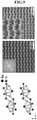
Fig. 5 shows a schematic view of the structure of Na2In2As3 and results of scanning transmission electron microscopy (STEM) analysis. The results of STEM analysis found that the synthesized Sample A had a P21/c space group. - As such, the results of
Figs. 2 to 5 found that the synthesized Sample A was Na2In2As3, a layered material having a new composition and a crystal structure having a P21/c space group. -
Fig. 6 shows changes in XRD peaks according to the removal of Na. In Sample A in which Na was not removed, the interplanar distance of the (002) plane was 7.42 Å, and as Na was removed, the interplanar distance gradually increased up to 7.47 Å. Changes in the XRD peaks as well were observed according to the changes in the interplanar distance, and it was found that with the removal of Na, the size of the peaks of the (102) plane to the peaks of the (002) plane gradually decreased. Accordingly, the value of I(102)/I(002) was 0.46 in Sample A, decreased to 0.13 in Sample B and to 0.09 in Sample D. In addition, when the XRD peaks were compared after the removal of Na, the (002) and (102) planes showed the same peaks, indicating that the crystal structure having a P21/c space group was kept. -
FIG. 7 shows a nanosheet prepared by removing Na from Sample A to become Sample C, and being peeled off from Sample C using a tape. In Sample A, a cleavage plane between the layers was observed, but in Sample C, as Na was removed, the interlayer distance increased, thereby forming cracks. -
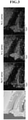
Fig. 8 shows an atomic force microscopy (AFM) image of a nanosheet prepared by being peeled off from Sample C and a line-profile therefrom. It was confirmed that a nanosheet was peeled off to have a thickness of 10 nm to 30 nm. -
Fig. 9 shows results of scanning transmission electron microscopy (STEM) analysis of Sample D. The data showed that Na was partially removed and there were no changes in the crystal structure even after the removal. -
Fig. 10 is results of TEM analysis of Sample E. It was found that an amorphous structure appeared with the excessive removal of Na. - Ferroelectric properties were measured through piezoresponse force microscopy (PFM) for the nanosheet peeled off from Sample C, and the results are shown in
FIG. 11 . It was found that the nanosheet had similar ferroelectric-like properties. - In addition, current changes according to voltages were measured for the nanosheet peeled off from Sample C, and results are shown in
Fig. 12 . - It was found that at an initial voltage, the nanosheet kept a
high resistance state 1, indicating a low current flow, but when the voltage was greater than a certain level, the nanosheet switched to alow resistance state 2, indicating a sharp increase in the current, and the same properties were shown in an opposite electrode direction, thereby showing resistance switching properties. - It was found that using the resistance switching properties, the nanosheet would be applied as a memristor device, which is being actively developed as a neuromorphic memory device.
Claims (15)
- A layered compound represented by Formula 1 below:
[Formula 1] Na1-xInyAsz
(0≤x<1.0, 0.8≤y≤1.2, 1.2≤z≤1.8) - The layered compound according to Claim 1, wherein, the x is 0.
- The layered compound according to Claim 1, wherein the x satisfies 0.1≤x≤0.9.
- The layered compound according to Claim 1, wherein the x satisfies 0.3≤x≤0.8.
- The layered compound according to one of Claims 1 to 4, wherein the layered compound further comprises H.
- The layered compound according to any one of Claims 1 to 5, wherein, in XRD measurement using CuKα rays, the layered compound has peaks at the positions of 2θ = 11.9°± 0.50°, 12.8°±0.50°, 13.5°±0.50°, 15.3°±0.50°, 21.6°±0.50°, 22.7°±0.50°, 23.8°±0.50°, and 27.8°±0.50°, the peaks having an intensity of 1% or greater with respect to a peak having the greatest intensity.
- The layered compound according to any one of Claims 1 to 6, wherein the crystal structure of the layered compound represents a space group of P21/c.
- The layered compound according to any one of Claims 1 to 7, wherein, in XRD measurement using CuKα rays, the layered compound has a I(102)/I(002) value of 0.40 or less which is a peak intensity of a (102) plane to a peak intensity of a (002) plane.
- The layered compound according to any one of Claims 1 to 8, wherein the layered compound exhibits ferroelectric-like properties.
- The layered compound according to any one of Claims 1 to 9, wherein the layered compound exhibits resistance switching properties.
- A nanosheet comprising a compound according to one of claims 1 to 10, and prepared through a physical or chemical peeling method.
- The nanosheet according to Claim 11, wherein the nanosheet has a thickness of 500 nm or less.
- An electrical device comprising the layered compound according to any one of Claims 1 to 9.
- An electrical device comprising the nanosheet according to Claims 11 or 12.
- The electrical device according to Claim 13 or 14, wherein the electrical device is a memristor.
Applications Claiming Priority (1)
| Application Number | Priority Date | Filing Date | Title |
|---|---|---|---|
| KR1020200117533A KR102425889B1 (en) | 2020-09-14 | 2020-09-14 | Layered compounds and nanosheets containing indium and arsenic, and electrical devices using the same |
Publications (1)
| Publication Number | Publication Date |
|---|---|
| EP3967652A1 true EP3967652A1 (en) | 2022-03-16 |
Family
ID=73792930
Family Applications (1)
| Application Number | Title | Priority Date | Filing Date |
|---|---|---|---|
| EP20211720.6A Pending EP3967652A1 (en) | 2020-09-14 | 2020-12-03 | Layered compound and nanosheet containing indium and arsenic, and electrical device using the same |
Country Status (4)
| Country | Link |
|---|---|
| US (1) | US11820669B2 (en) |
| EP (1) | EP3967652A1 (en) |
| JP (1) | JP7116498B2 (en) |
| KR (1) | KR102425889B1 (en) |
Citations (2)
| Publication number | Priority date | Publication date | Assignee | Title |
|---|---|---|---|---|
| US20190352799A1 (en) * | 2018-05-18 | 2019-11-21 | Industry-Academic Cooperation Foundation, Yonsei University | LAYERED GaAs, METHOD OF PREPARING SAME, AND GaAs NANOSHEET EXFOLIATED FROM SAME |
| KR20190132294A (en) * | 2018-05-18 | 2019-11-27 | 연세대학교 산학협력단 | Layered InAs, manufacturing method thereof and InAs nanosheet exfoliated therefrom |
Family Cites Families (2)
| Publication number | Priority date | Publication date | Assignee | Title |
|---|---|---|---|---|
| US10662074B2 (en) * | 2016-12-30 | 2020-05-26 | Nanoco Technologies Ltd. | Template-assisted synthesis of 2D nanosheets using nanoparticle templates |
| KR102271060B1 (en) * | 2018-05-18 | 2021-06-29 | 연세대학교 산학협력단 | Layered AlN, manufacturing method thereof and exfoliated AlN nanosheet therefrom |
-
2020
- 2020-09-14 KR KR1020200117533A patent/KR102425889B1/en active Active
- 2020-12-03 US US17/111,003 patent/US11820669B2/en active Active
- 2020-12-03 EP EP20211720.6A patent/EP3967652A1/en active Pending
- 2020-12-03 JP JP2020201196A patent/JP7116498B2/en active Active
Patent Citations (2)
| Publication number | Priority date | Publication date | Assignee | Title |
|---|---|---|---|---|
| US20190352799A1 (en) * | 2018-05-18 | 2019-11-21 | Industry-Academic Cooperation Foundation, Yonsei University | LAYERED GaAs, METHOD OF PREPARING SAME, AND GaAs NANOSHEET EXFOLIATED FROM SAME |
| KR20190132294A (en) * | 2018-05-18 | 2019-11-27 | 연세대학교 산학협력단 | Layered InAs, manufacturing method thereof and InAs nanosheet exfoliated therefrom |
Also Published As
| Publication number | Publication date |
|---|---|
| JP7116498B2 (en) | 2022-08-10 |
| US20220081314A1 (en) | 2022-03-17 |
| US11820669B2 (en) | 2023-11-21 |
| KR102425889B1 (en) | 2022-07-26 |
| KR20220035597A (en) | 2022-03-22 |
| JP2022048061A (en) | 2022-03-25 |
Similar Documents
| Publication | Publication Date | Title |
|---|---|---|
| Cordero et al. | Probing ferroelectricity in highly conducting materials through their elastic response: Persistence of ferroelectricity in metallic BaTiO 3− δ | |
| US11691891B2 (en) | Layered group III-V compound including additive elements and having ferroelectric-like properties, and nanosheet using the same | |
| US11820669B2 (en) | Layered compound and nanosheet containing indium and arsenic, and electrical device using the same | |
| EP3967658B1 (en) | Layered compound and nanosheet containing indium and phosphorus, and electrical device using the same | |
| US11634340B2 (en) | Layered group III-V compound and nanosheet containing arsenic, and electrical device using the same | |
| KR102425888B1 (en) | Layered compounds and nanosheets containing gallium and arsenic, and electrical devices using the same | |
| KR102453020B1 (en) | Layered compounds and nanosheets containing Zinc and Sulfur, and electrical devices using the same | |
| KR102425893B1 (en) | Layered compounds and nanosheets containing potassium, indium and arsenic, and electrical devices using the same | |
| US11597651B2 (en) | Layered group III-V compound and nanosheet containing phosphorus, and electrical device using the same | |
| KR102425894B1 (en) | Layered compounds and nanosheets containing indium and antimony, and electrical devices using the same | |
| US11643753B2 (en) | Layered group III-V compound and nanosheet containing antimony, and electrical device using the same | |
| KR102484718B1 (en) | Layered compounds and nanosheets containing gallium and arsenic, and electrical devices using the same | |
| KR102425890B1 (en) | Layered compounds and nanosheets containing aluminum and antimony, and electrical devices using the same | |
| KR102425891B1 (en) | Layered compounds and nanosheets containing gallium and antimony, and electrical devices using the same | |
| KR102514683B1 (en) | Layered compounds and nanosheets containing indium and phosphorus, and electrical devices using the same | |
| KR102479782B1 (en) | Layered GaP, GaP nanosheet and Electrical Dvice using the Same | |
| US11840458B2 (en) | Layered GaN and GaN nanosheet, and electrical device using the same | |
| Pascual-González et al. | Point defect engineering of high temperature piezoelectric BiScO3-PbTiO3 for high power operation | |
| SHEETS et al. | Special Issue Ceramics Integration. Liquid-Phase Epitaxial Growth of BaTiO3 Doped (Na0. 5Bi0. 5) TiO3 Single Crystals on a SrTiO3 Single Crystal Substrate. |
Legal Events
| Date | Code | Title | Description |
|---|---|---|---|
| PUAI | Public reference made under article 153(3) epc to a published international application that has entered the european phase |
Free format text: ORIGINAL CODE: 0009012 |
|
| STAA | Information on the status of an ep patent application or granted ep patent |
Free format text: STATUS: THE APPLICATION HAS BEEN PUBLISHED |
|
| AK | Designated contracting states |
Kind code of ref document: A1 Designated state(s): AL AT BE BG CH CY CZ DE DK EE ES FI FR GB GR HR HU IE IS IT LI LT LU LV MC MK MT NL NO PL PT RO RS SE SI SK SM TR |
|
| STAA | Information on the status of an ep patent application or granted ep patent |
Free format text: STATUS: REQUEST FOR EXAMINATION WAS MADE |
|
| 17P | Request for examination filed |
Effective date: 20220914 |
|
| RBV | Designated contracting states (corrected) |
Designated state(s): AL AT BE BG CH CY CZ DE DK EE ES FI FR GB GR HR HU IE IS IT LI LT LU LV MC MK MT NL NO PL PT RO RS SE SI SK SM TR |