EP3967115B1 - Leitfähige übertragung und herstellungsverfahren dafür - Google Patents
Leitfähige übertragung und herstellungsverfahren dafür Download PDFInfo
- Publication number
- EP3967115B1 EP3967115B1 EP20726513.3A EP20726513A EP3967115B1 EP 3967115 B1 EP3967115 B1 EP 3967115B1 EP 20726513 A EP20726513 A EP 20726513A EP 3967115 B1 EP3967115 B1 EP 3967115B1
- Authority
- EP
- European Patent Office
- Prior art keywords
- conductive
- transfer
- article
- layer
- conductive transfer
- Prior art date
- Legal status (The legal status is an assumption and is not a legal conclusion. Google has not performed a legal analysis and makes no representation as to the accuracy of the status listed.)
- Active
Links
Images






Classifications
-
- B—PERFORMING OPERATIONS; TRANSPORTING
- B32—LAYERED PRODUCTS
- B32B—LAYERED PRODUCTS, i.e. PRODUCTS BUILT-UP OF STRATA OF FLAT OR NON-FLAT, e.g. CELLULAR OR HONEYCOMB, FORM
- B32B3/00—Layered products comprising a layer with external or internal discontinuities or unevennesses, or a layer of non-planar shape; Layered products comprising a layer having particular features of form
- B32B3/10—Layered products comprising a layer with external or internal discontinuities or unevennesses, or a layer of non-planar shape; Layered products comprising a layer having particular features of form characterised by a discontinuous layer, i.e. formed of separate pieces of material
- B32B3/12—Layered products comprising a layer with external or internal discontinuities or unevennesses, or a layer of non-planar shape; Layered products comprising a layer having particular features of form characterised by a discontinuous layer, i.e. formed of separate pieces of material characterised by a layer of regularly- arranged cells, e.g. a honeycomb structure
-
- A—HUMAN NECESSITIES
- A61—MEDICAL OR VETERINARY SCIENCE; HYGIENE
- A61N—ELECTROTHERAPY; MAGNETOTHERAPY; RADIATION THERAPY; ULTRASOUND THERAPY
- A61N1/00—Electrotherapy; Circuits therefor
- A61N1/02—Details
- A61N1/04—Electrodes
- A61N1/0404—Electrodes for external use
- A61N1/0408—Use-related aspects
- A61N1/0452—Specially adapted for transcutaneous muscle stimulation [TMS]
-
- A—HUMAN NECESSITIES
- A61—MEDICAL OR VETERINARY SCIENCE; HYGIENE
- A61N—ELECTROTHERAPY; MAGNETOTHERAPY; RADIATION THERAPY; ULTRASOUND THERAPY
- A61N1/00—Electrotherapy; Circuits therefor
- A61N1/02—Details
- A61N1/04—Electrodes
- A61N1/0404—Electrodes for external use
- A61N1/0472—Structure-related aspects
- A61N1/0484—Garment electrodes worn by the patient
-
- B—PERFORMING OPERATIONS; TRANSPORTING
- B32—LAYERED PRODUCTS
- B32B—LAYERED PRODUCTS, i.e. PRODUCTS BUILT-UP OF STRATA OF FLAT OR NON-FLAT, e.g. CELLULAR OR HONEYCOMB, FORM
- B32B7/00—Layered products characterised by the relation between layers; Layered products characterised by the relative orientation of features between layers, or by the relative values of a measurable parameter between layers, i.e. products comprising layers having different physical, chemical or physicochemical properties; Layered products characterised by the interconnection of layers
- B32B7/04—Interconnection of layers
- B32B7/12—Interconnection of layers using interposed adhesives or interposed materials with bonding properties
-
- B—PERFORMING OPERATIONS; TRANSPORTING
- B41—PRINTING; LINING MACHINES; TYPEWRITERS; STAMPS
- B41M—PRINTING, DUPLICATING, MARKING, OR COPYING PROCESSES; COLOUR PRINTING
- B41M3/00—Printing processes to produce particular kinds of printed work, e.g. patterns
- B41M3/12—Transfer pictures or the like, e.g. decalcomanias
-
- H—ELECTRICITY
- H05—ELECTRIC TECHNIQUES NOT OTHERWISE PROVIDED FOR
- H05K—PRINTED CIRCUITS; CASINGS OR CONSTRUCTIONAL DETAILS OF ELECTRIC APPARATUS; MANUFACTURE OF ASSEMBLAGES OF ELECTRICAL COMPONENTS
- H05K3/00—Apparatus or processes for manufacturing printed circuits
- H05K3/0058—Laminating printed circuit boards onto other substrates, e.g. metallic substrates
-
- H—ELECTRICITY
- H05—ELECTRIC TECHNIQUES NOT OTHERWISE PROVIDED FOR
- H05K—PRINTED CIRCUITS; CASINGS OR CONSTRUCTIONAL DETAILS OF ELECTRIC APPARATUS; MANUFACTURE OF ASSEMBLAGES OF ELECTRICAL COMPONENTS
- H05K3/00—Apparatus or processes for manufacturing printed circuits
- H05K3/10—Apparatus or processes for manufacturing printed circuits in which conductive material is applied to the insulating support in such a manner as to form the desired conductive pattern
- H05K3/20—Apparatus or processes for manufacturing printed circuits in which conductive material is applied to the insulating support in such a manner as to form the desired conductive pattern by affixing prefabricated conductor pattern
- H05K3/207—Apparatus or processes for manufacturing printed circuits in which conductive material is applied to the insulating support in such a manner as to form the desired conductive pattern by affixing prefabricated conductor pattern using a prefabricated paste pattern, ink pattern or powder pattern
-
- A—HUMAN NECESSITIES
- A61—MEDICAL OR VETERINARY SCIENCE; HYGIENE
- A61B—DIAGNOSIS; SURGERY; IDENTIFICATION
- A61B5/00—Measuring for diagnostic purposes; Identification of persons
- A61B5/68—Arrangements of detecting, measuring or recording means, e.g. sensors, in relation to patient
- A61B5/6801—Arrangements of detecting, measuring or recording means, e.g. sensors, in relation to patient specially adapted to be attached to or worn on the body surface
- A61B5/6802—Sensor mounted on worn items
- A61B5/6804—Garments; Clothes
-
- B—PERFORMING OPERATIONS; TRANSPORTING
- B32—LAYERED PRODUCTS
- B32B—LAYERED PRODUCTS, i.e. PRODUCTS BUILT-UP OF STRATA OF FLAT OR NON-FLAT, e.g. CELLULAR OR HONEYCOMB, FORM
- B32B2307/00—Properties of the layers or laminate
- B32B2307/20—Properties of the layers or laminate having particular electrical or magnetic properties, e.g. piezoelectric
- B32B2307/202—Conductive
-
- B—PERFORMING OPERATIONS; TRANSPORTING
- B32—LAYERED PRODUCTS
- B32B—LAYERED PRODUCTS, i.e. PRODUCTS BUILT-UP OF STRATA OF FLAT OR NON-FLAT, e.g. CELLULAR OR HONEYCOMB, FORM
- B32B2307/00—Properties of the layers or laminate
- B32B2307/20—Properties of the layers or laminate having particular electrical or magnetic properties, e.g. piezoelectric
- B32B2307/206—Insulating
-
- H—ELECTRICITY
- H05—ELECTRIC TECHNIQUES NOT OTHERWISE PROVIDED FOR
- H05K—PRINTED CIRCUITS; CASINGS OR CONSTRUCTIONAL DETAILS OF ELECTRIC APPARATUS; MANUFACTURE OF ASSEMBLAGES OF ELECTRICAL COMPONENTS
- H05K1/00—Printed circuits
- H05K1/02—Details
- H05K1/03—Use of materials for the substrate
- H05K1/038—Textiles
-
- H—ELECTRICITY
- H05—ELECTRIC TECHNIQUES NOT OTHERWISE PROVIDED FOR
- H05K—PRINTED CIRCUITS; CASINGS OR CONSTRUCTIONAL DETAILS OF ELECTRIC APPARATUS; MANUFACTURE OF ASSEMBLAGES OF ELECTRICAL COMPONENTS
- H05K1/00—Printed circuits
- H05K1/02—Details
- H05K1/09—Use of materials for the conductive, e.g. metallic pattern
- H05K1/092—Dispersed materials, e.g. conductive pastes or inks
- H05K1/095—Dispersed materials, e.g. conductive pastes or inks for polymer thick films, i.e. having a permanent organic polymeric binder
-
- H—ELECTRICITY
- H05—ELECTRIC TECHNIQUES NOT OTHERWISE PROVIDED FOR
- H05K—PRINTED CIRCUITS; CASINGS OR CONSTRUCTIONAL DETAILS OF ELECTRIC APPARATUS; MANUFACTURE OF ASSEMBLAGES OF ELECTRICAL COMPONENTS
- H05K2201/00—Indexing scheme relating to printed circuits covered by H05K1/00
- H05K2201/01—Dielectrics
- H05K2201/0183—Dielectric layers
- H05K2201/0195—Dielectric or adhesive layers comprising a plurality of layers, e.g. in a multilayer structure
-
- H—ELECTRICITY
- H05—ELECTRIC TECHNIQUES NOT OTHERWISE PROVIDED FOR
- H05K—PRINTED CIRCUITS; CASINGS OR CONSTRUCTIONAL DETAILS OF ELECTRIC APPARATUS; MANUFACTURE OF ASSEMBLAGES OF ELECTRICAL COMPONENTS
- H05K2201/00—Indexing scheme relating to printed circuits covered by H05K1/00
- H05K2201/09—Shape and layout
- H05K2201/09209—Shape and layout details of conductors
- H05K2201/09654—Shape and layout details of conductors covering at least two types of conductors provided for in H05K2201/09218 - H05K2201/095
- H05K2201/09681—Mesh conductors, e.g. as a ground plane
-
- H—ELECTRICITY
- H05—ELECTRIC TECHNIQUES NOT OTHERWISE PROVIDED FOR
- H05K—PRINTED CIRCUITS; CASINGS OR CONSTRUCTIONAL DETAILS OF ELECTRIC APPARATUS; MANUFACTURE OF ASSEMBLAGES OF ELECTRICAL COMPONENTS
- H05K3/00—Apparatus or processes for manufacturing printed circuits
- H05K3/10—Apparatus or processes for manufacturing printed circuits in which conductive material is applied to the insulating support in such a manner as to form the desired conductive pattern
- H05K3/12—Apparatus or processes for manufacturing printed circuits in which conductive material is applied to the insulating support in such a manner as to form the desired conductive pattern using thick film techniques, e.g. printing techniques to apply the conductive material or similar techniques for applying conductive paste or ink patterns
- H05K3/1216—Apparatus or processes for manufacturing printed circuits in which conductive material is applied to the insulating support in such a manner as to form the desired conductive pattern using thick film techniques, e.g. printing techniques to apply the conductive material or similar techniques for applying conductive paste or ink patterns by screen printing or stencil printing
Definitions
- the present invention relates to a conductive transfer, an article comprising a conductive transfer and a method of producing a conductive transfer.
- Conductive transfers such as that disclosed by the applicant in patent GB 2 555 592 provide a means by which thin, lightweight and washable conductive elements can be incorporated into flexible items, for example, wearable items such as items of clothing. Such transfers may provide an electrical circuit to an electronic device utilised as part of the clothing. In some applications, the conductive transfer covers a large area of the clothing requiring large amounts of conductive ink to be used.
- US 2008/083721 (Kaiserman, Terrance et al ) describes a heated textile comprising a conductive layer disposed between two dielectric layers.
- the conductive layer comprises a conductive ink composition and defines a circuit.
- the disclosure indicates that the ink used to form the conductive layer should be chosen to provide flexibility and durability of the conductive layer.
- US 2019/053372 (Kwon, Euichul et al ) describes a garment-type electronic device comprising electrical wiring using stretchable conductor composition.
- the disclosure seeks to ensure a lack of level difference at the boundary of the electrode surface to reduce discomfort during wearing of an item.
- US 2004/051082 (Child, Andrew D et al ) describes a static dissipative textile having an electrically conductive surface comprising an electrically conductive coating.
- the conductive coating includes a pattern to provide a static dissipative textile.
- a conductive transfer in accordance with the present invention aims to provide a suitable transfer which can be utilised in a wide variety of applications utilising conventional manufacturing techniques and which can withstand conventional washing techniques and standard use.
- conductive transfer 101 An example of such a conductive transfer which is suitable for application to an article, is represented in cross sectional schematic view as conductive transfer 101. It is appreciated that, in this schematic view, conductive transfer 101 is shown having increased thickness. In practice, conductive transfer 101 is typically in the region of between half a millimetre (0.5 mm) and five millimetres (5 mm) in thickness.
- Conductive transfer 101 comprises a first non-conductive layer 102 and a second non-conductive layer 103. Conductive transfer 101 further comprises a conductive layer 104, which is positioned between first non-conductive layer 102 and second non-conductive layer 103. Conductive transfer 101 also comprises an adhesive layer 105 which is suitable for adhering the conductive transfer to an article, such as the wearable item depicted in Figure 8 .
- each of the layers are printed onto a transfer substrate 106 which can be removed following an application of heat and/or pressure in line with the method of producing the conductive transfer as will be described with respect to Figure 5 .
- first non-conductive layer 102 is printed onto transfer substrate 106 , with the following layers being printed thereon in sequence of conductive layer 104, non-conductive layer 103 and adhesive layer 105.
- non-conductive layer 102 is printed in an arrangement which produces areas of non-conductive ink and areas without non-conductive ink.
- portions 107 and 108 of non-conductive layer 102 provide areas of non-conductive ink and portion 109 presents an area in non-conductive layer 102 which does not comprise non-conductive ink. Consequently, when conductive layer 104 is printed, conductive ink covers portion 109 to provide a section of conductive ink which can be used as an electrical contact point as part of an electrical circuit.
- non-conductive layers 102 and 103 comprise any suitable printing ink for encapsulating the conductive layer 104.
- a suitable printing ink may include a water-based printing ink; an ultraviolet cured printing ink; a solvent based ink; or a latex printing ink. It is appreciated that, in alternative embodiments, other suitable non-conductive encapsulating inks may be utilised.
- conductive layer 104 comprises any suitable conductive printing ink, for example, a conductive ink comprising silver. Other conductive inks such as those including copper may also be utilised.
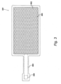
- FIG. 2 A plan view of conductive transfer 101 falling outside the scope of the claimed invention is illustrated in Figure 2 .
- conductive transfer 101 has been applied to a textile 201.
- Conductive transfer 101 comprises a plurality of tessellated cells 202 which are defined by conductive layer 104 and a printed conductive ink.
- non-conductive layer 102 has also been printed in a form that is substantially similar to the pattern of conductive layer 103.
- non-conductive layer 102 is also considered to comprise a plurality of tessellated cells.
- tessellated cells 202 are arranged to form a grid-like pattern. It is appreciated that the tessellated cells may be arranged in any suitable grid-like pattern, and example embodiments herein present possible variations in the tessellated cells rather than an exhaustive list.
- Conductive transfer 101 further comprises electrical contacts 203A and 203B. These electrical contacts correspond to the portion 109 previously indicated in Figure 1 and provide access to conductive layer 104 to allow an electrical current to be supplied to conductive layer 104 to provide functionality to the transfer.
- FIG. 3 A further example embodiment of a conductive transfer falling outside the scope of the present invention is shown in Figure 3 in plan view.
- Conductive transfer 301 comprises first and second non-conductive layers in a substantially similar manner to those as illustrated in respect of conductive transfer 101. Between the two non-conductive layers is a conductive layer which comprises a plurality of tessellated cells 302 defined by a printed conductive ink.
- the plurality of tessellated cells are arranged in the form of a honeycomb pattern over a main element 303 of the conductive layer.
- the conductive layer of transfer 301 comprises main element 303 and an input track 304, which is shown as dashed lines to illustrate where it is partially overprinted by one of the non-conductive layers.
- Input track 304 extends towards one end of conductive transfer 301 and presents an exposed electrical contact point 305 which can be used to connect to, for example, a power source to provide an electric current to the conductive layer.
- input track 304 is printed in the form of a solid input track of conductive ink which connects to main element 303 which is printed in the form of honeycomb tessellated cells.
- the upper non-conductive layer is printed on the conductive layer and includes an open portion which allows for the creation of contact point 305.
- first non-conductive layer is printed in a substantially similar honeycomb pattern over the conductive layer.
- second non-conductive layer may be printed with a substantially similar honeycomb pattern.
- second non-conductive layer is printed as a solid main element.
- each of the tessellated cells includes an inner cell which is absent of conductive material.
- the outline of the tessellated pattern in this case the honeycomb pattern, reduces the volume or quantity of ink required to print a given sized conductive transfer. This in turn reduces the weight of the conductive transfer which can be particularly desirable in respect of transfers which are provided for use with wearable items.
- the inner cells provide apertures in the conductive layer which improves the flexibility and stretchability of the tessellated area. This allows the transfer to be applied to conventional stretchable textiles without loss of functionality.
- a patterned tessellation such as the honeycomb pattern shown in Figure 3 also provides an even electrical current flow when an electrical current is provided via contact point 305.
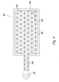
- FIG. 4 An alternative example embodiment of a conductive transfer in accordance with the present invention is shown in Figure 4 in plan view.
- Conductive transfer 401 comprises first and second non-conductive layers and a conductive layer positioned between the two non-conductive layers in a substantially similar manner to conductive transfer 101 as shown in Figure 1 .
- conductive transfer 401 comprises a conductive layer which comprises a plurality of tessellated cells 402 defined by a printed conductive ink.
- each triangular cell includes an inner cell, for example inner cell 404, in which conductive ink has not been printed.
- conductive transfer 401 comprises a main element 405 and an input track 406.
- the plurality of tessellated cells 402 are comprised over both main element 405 and input track 406. Consequently, input track 406 can have increased flexibility and stretchability. It is appreciated that, for a particular application, the cross-sectional area of the input track in part determines the amount of electrical current which can flow along the input track. Consequently, in some embodiments, input track 406 may have an increased cross-sectional area to ensure a desired electrical current is achieved.
- input track 406 extends from main element 405 towards one end whereby the non-conductive layer provides a portion which is utilised as an electrical contact point 407.
- the tessellated cells are arranged in a triangular packing pattern.
- the tessellated cells are arranged in a circular packing arrangement.
- any other suitable packing arrangement may be utilised for the tessellated cells as desired, however, in each embodiment in accordance with the claimed invention the tessellated cells are such that they comprise a cell with an outline defined by the conductive ink and an inner cell which is substantially absent of conductive ink so as to present an aperture in the conductive layer.
- first non-conductive layer of conductive transfer 401 also comprises a substantially similar triangular packing pattern.
- first non-conductive layer of conductive transfer 401 may be printed as a solid input track and main element.
- the non-conductive layer may comprise an alternative patterned effect. In one example, this patterned effect may be simulated to give the appearance of another material, for example, leather.
- the conductive transfer may be utilised on the surface of another item or textile such as a car seat, car interior or similar. In one embodiment, the conductive transfer may be used to provide a circuit for a heated seat.
- FIG. 5 A schematic diagram showing a method of producing any of conductive transfers described herein is shown in Figure 5 .
- a suitable non-conductive ink is printed onto a transfer substrate, such as substrate 106 to produce a first non-conductive layer.
- the first non-conductive layer may be cured as necessary before an electrically conductive ink is printed thereon at step 502. This step thereby produces a conductive layer, which again may undergo any suitable curing process.
- the electrically conductive ink is printed in a pattern which comprises a plurality of tessellated cells which are defined by the printed conductive ink.
- substantially similar non-conductive ink is printed over the conductive layer to produce a second non-conductive layer.
- the second non-conductive layer may undergo a suitable curing process to ensure it is suitable for application of the adhesive material.
- the adhesive material is printed over the second non-conductive layer to produce the adhesive layer. A further curing step may be included thereafter.
- Steps 505 to 507 provide a method of attaching the conductive transfer to an article.
- the conductive transfer is positioned onto an article.
- the adhesive layer is brought into contact with the article such that the transfer substrate 106 is furthest away from the surface of the article.
- an application of heat, pressure or a combination of both heat and pressure is applied to the transfer such that the adhesive layer allows the transfer to adhere to the article.
- transfer substrate 106 can be peeled away and removed leaving the first non-conductive layer as the top surface of the transfer on the article.
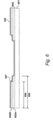
- the aforementioned printing method may include printing additional layers of material in the manner described in Figure 6 .
- transfer substrate 601 has, in accordance with step 501 described previously, has a non-conductive layer 602 printed thereon.
- non-conductive layer 602 comprises a first printed ink layer 602A and a second printed ink layer 602B which have been printed separately. In this way, a first pass of the printing method is made to produce layer 602A, and a second pass is made to produce layer 602B.
- Conductive layer 603 is printed over the non-conductive layer in line with step 502.
- conductive layer 603 forms a contact point 604 as illustrated.
- known non-conductive layers provide a waterfall-effect of the conductive layer over the edge of the non-conductive layer. This can lead to instability in the conductive layer and may lead to breakages.
- printed ink layer 602A comprises a first length 605
- printed ink layer 602B comprises a second length 606. Second length 606 is shorter than first length 605 and, a step 607 is formed between the first and second printed ink layers.
- FIG. 7 A further illustration of the increased durability of the conductive transfer described herein is shown in Figure 7 , whereby, in respect of conductive transfer 701 , the cross-sectional area of the interface between the input track 702 and main element 703 has been increased. In all other respects, conductive transfer 701 can be considered substantially similar to conductive transfer 301.
- the conductive transfer has been widened to include a substantially spherical interface 704 which comprises an increased cross-sectional area.
- the width of input track 702 is less than the diameter of the spherical interface 704.
- any of the conductive transfers described herein may be utilised and attached to any suitable article.
- Examples include a wearable item, a heated seat, a heated blanket, a heat sensor, a medical bandage, a medical pad or a heated pad. It is appreciated however, that this list should not be considered exhaustive.
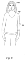
- any of the aforementioned conductive transfers may be applied to the wearable item of Figure 8 .
- a conductive transfer of the type herein described is applied to wearable item 801.
- Wearable item 801 is a conventional top or shirt and conductive transfer 802 is applied on the inside of a sleeve of the wearable item.
- conductive transfer 802 is configured to provide electrical muscle stimulation (EMS) and is incorporated into wearable item 801 such that is it able to be worn close to the skin of wearer 803 and apply EMS to the wearer.
- EMS electrical muscle stimulation
- conductive transfer 802 in this embodiment is worn close to the skin of the user's arm
- wearable items incorporating conductive transfers for use close to the skin may be provided in any embodiments relating to, but not limited to the following: sexual health, urinary & faecal incontinence, pain relief and management, toning & strengthening of muscles, neuromuscular rehabilitation, orthopaedic rehabilitation, muscle control in the avoidance of injuries.
- the conductive transfer is configured to measure vital signs of a wearer of an article to produce an electrocardiogram (ECG).
- ECG Electroencephalogram
- EMG Electromyogram
- GSR Galvanic skin response
- MEG Magnetoencephalogram
- conductive transfer 802 is configure to provide EMS to wearer 803, in particular in relation to wearer 803 's arm.
- conductive transfer 802 is configured to have a plurality of activation zones.
- a first plurality of tessellated cells may correspond to a first activation zone and a second plurality of tessellated cells may correspond to a second activation zone.
- wearer 803 can ensure that a specific activation zone can be utilised for muscle stimulation.
- Providing a conductive transfer with tessellated cells also provides a degree of breathability as the spaces in the cells mean that when applied to a textile or wearable item, air is more easily able to pass through.
- conventional conductive transfers typically print transfers for such applications in the form of solid conductive layers, in some embodiments whereby the conductive transfer is incorporated into a wearable item, the solid print can cause the transfer to slide around and lose contact with the muscle area to which stimulation is required.
- the tessellated cells provide an addition grip due to the breaks in the pattern ensuring that the transfer stays in the intended position so that stimulation is retained at the point of interest.
- wearable items comprise seams whereby a one or more textile panels can be brought together to result in a wearable item.
- a textile panel 901 has been provided with an aperture 902 therethrough.
- Textile panel 901 comprises a first top surface 903 and a second bottom surface 904, which is position substantially opposite to surface 903.
- conductive transfer 905 is affixed to textile panel 901 by positioning conductive transfer 905 through aperture 902 and affixing the conductive transfer 905 to both first surface 903 and second surface 904. This may be achieved by the application of heat and/or pressure previously indicated once the conductive transfer has been positioned through aperture 902.
- a particular advantage of the tessellated cells of the present invention means that, when incorporated into a textile which requires stitching, a stitch which penetrates the conductive transfer, whether intended or not, is less likely to have a negative effect on the operational functionality of the transfer.
- stitching may be specifically designed to ensure that during manufacture, the stitches in the fabric and potentially across the conductive transfer penetrate through the tessellated cells themselves rather than the conductive trace on the conductive layer.
- a stitch may penetrate part of the conductive trace without any adverse effects.
- the textile comprises a seam comprising at least one stitch and the at least one stitch penetrates the textile via a point within a first one of the tessellated cells.
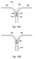
- a first textile panel 1001 and a second textile panel 1002 are arranged to form a seam 1003.
- Each textile panel 1001 and 1002 comprises and aperture 1004 and 1005 respectively through which conductive transfers 1006 and 1007 respectively are positioned therethrough.
- an anisotropic conductive film (ACF) 1008 is positioned between textile panel 1001 and textile panel 1002 thereby providing an electrical connection through ACF bonding.
- Anisotropic conductive film (ACF) is a known film which is used to bond components together following the application of heat and pressure. It is appreciated that, alternatives to ACF may be utilised in alternative embodiments, for example, conductive adhesives, low temperature solder or cured inks such as silver.
- FIG 10B once textile panels 1001 and 1003 have been brought together and bonded, a conventional stitching process can be carried out.
- a first stitch 1009 is positioned across the seam 1003 and a conventional overlocking stitch 1010, performed by an overlocker sewing machine, is used to hold the textile panels together.
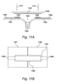
- FIG. 11A A further example showing the incorporation of a conductive transfer into an article comprising textile panels is shown in Figures 11A and 11B .
- Figure 11A shows textile panel 1101 and textile panel 1102 which form a seam 1103 and which are joined by means of an overlocker stitch 1104.
- Textile panel 1101 comprises conductive transfer 1105
- textile panel 1102 comprises a conductive transfer 1106.
- conductive transfer 1105 and conductive transfer 1106 each include contact points in which it is desirable that those contact points are connected to each other across seam 1103.
- further anisotropic conductive film (ACF) 1107 and 1108 respectively is positioned over each of the contact points of conductive transfer 1105 and conductive transfer 1106.
- ACF anisotropic conductive film
- a textile element 1109 which comprises a further conductive transfer 1110 is placed over the conductive transfer 1105 and 1106 and their respective contact points.
- Conductive transfer 1110 has corresponding contact points which are configured to cooperate with those of conductive transfer 1105 and conductive transfer 1106.
- Figure 11B shows a plan view of the arrangement from the top above textile element 1109. With textile panels 1101 and 1102 now joined, additional stitching 1112 can be added to provide extra strengthening across seam 1103.
- a conductive transfer of the type described herein can further be connected to an electronic component such as a power source, for example, a battery, a printed circuit board, a connector or any other suitable or required electronic component.
- a power source for example, a battery, a printed circuit board, a connector or any other suitable or required electronic component.
- a textile panel 1201 comprising a conductive transfer 1202 is provided, along with any suitable electronic component 1203, such as those previously described.
- Conductive transfer 1202 includes a contact point which requires connection to electronic component 1203, which also includes a corresponding contact point for making an electrical connection.
- anisotropic conductive film (ACF) 1204 and 1205 is placed respectively on the contact points of conductive transfer 1201 and electronic component 1203.
- a textile element 1206 which comprises a conductive transfer 1207, which again includes two corresponding contact points on its surface.
- a further textile element 1208 sandwiches conductive transfer 1207 between textile element 1206 and textile element 1208 while retaining exposure to the two contact points of conductive transfer 1207.
- Textile element 1208 provides a clean undersurface which also obscures the view of conductive transfer 1207 in use and presents a textile appearance on the undersurface.
- Figure 12B shows a corresponding plan view, whereby conductive transfer 1202 is connected to electronic component 1203. Again, additional stitching 1210 can be provided to strengthen the seams of the textile or wearable item.
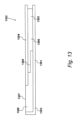
- Figure 13 shows a section of input track 1301 of a conductive transfer 1302.
- Conductive transfer 1301 comprises non-conductive layer 1303 and non-conductive layer 1302 which are substantially similar to the non-conductive layers described previously.
- a first, highly conductive material 1306 is printed across the conductive layer in the portion which, in the finished conductive transfer 1302, is encapsulated by non-conductive layer 1303 and non-conductive layer 1304.
- a second highly washable material 1308 is printed.
- highly washable material 1308 comprises a conductive polymer which comprises a PEDOT/PSS (3,4 polyethylene dioxythiophene base material.
- Highly conductive material 1306 comprises a stretchable silver ink. This arrangement keeps the conductive material 1306 away from being exposed to a standard wash, for example of a wearable item in a washing machine.
- a contact zone 1309 Between the highly conductive material 1306 and the highly washable material 1308 is a contact zone 1309 which ensures a good connection between the two materials.
Landscapes
- Engineering & Computer Science (AREA)
- Health & Medical Sciences (AREA)
- Life Sciences & Earth Sciences (AREA)
- Animal Behavior & Ethology (AREA)
- Veterinary Medicine (AREA)
- Public Health (AREA)
- Biomedical Technology (AREA)
- General Health & Medical Sciences (AREA)
- Nuclear Medicine, Radiotherapy & Molecular Imaging (AREA)
- Radiology & Medical Imaging (AREA)
- Microelectronics & Electronic Packaging (AREA)
- Manufacturing & Machinery (AREA)
- Physics & Mathematics (AREA)
- Biophysics (AREA)
- Pathology (AREA)
- Heart & Thoracic Surgery (AREA)
- Medical Informatics (AREA)
- Molecular Biology (AREA)
- Surgery (AREA)
- Manufacturing Of Printed Wiring (AREA)
Claims (19)
- Eine leitfähige Übertragung (101, 201, 301, 401, 701, 802, 905, 1006, 1007) zum Aufbringen auf ein Objekt (801), welches Folgendes umfasst:eine erste, nichtleitende Schicht (102, 602) und eine zweite, nicht leitende Schicht (103);eine leitende Schicht (104, 603), die zwischen der ersten nichtleitenden Schicht und der zweiten nicht leitenden Schicht positioniert ist; undeine Klebstoffschicht (105) zum Anbringen der leitfähigen Übertragung an einem Objekt, wobeidie leitfähige Schicht eine Vielzahl mosaikartiger Zellen (302, 402) umfasst, die durch eine aufgedruckte leitfähige Druckfarbe definiert sind, wobei die mosaikartigen Zellen so angeordnet sind, dass sie ein gitterförmiges Raster bilden, wobei jede der mosaikartigen Zellen eine innere Zelle (404) enthält, die kein leitfähiges Material enthält, und dadurch gekennzeichnet ist, dass:die leitfähige Schicht ein Hauptelement (303, 405, 703) und eine Eingangsspur (304, 406, 702) umfasst und die Vielzahl der mosaikartigen Zellen über dem Hauptelement und der Eingangsspur der leitfähigen Schicht enthalten ist;die besagte erste nichtleitende Schicht eine erste gedruckte Druckfarbenschicht (602A) und eine zweite gedruckte Druckfarbenschicht (602B) umfasst, wobei die besagte erste gedruckte Druckfarbenschicht eine erste Länge (605) umfasst; unddie zweite gedruckte Druckfarbenschicht eine zweite Länge (606) aufweist, die kürzer als die erste Länge ist, und die zweite gedruckte Druckfarbenschicht die erste gedruckte Druckfarbenschicht überlagert, um eine Stufe (607) zwischen der ersten und der zweiten gedruckten Druckfarbenschicht zu bilden.
- Leitfähige Übertragung nach Anspruch 1, wobei die mosaikartigen Zellen in Form einer der folgenden Formen angeordnet sind:
Wabenmuster, kreisförmige Anordnung oder dreieckige Anordnung (403). - Leitfähige Übertragung nach Anspruch 1 oder Anspruch 2, wobei die Eingabespur eine Druckfarbe mit einem leitfähigen Polymer umfasst.
- Leitfähige Übertragung nach einem der voranstehenden Ansprüche, wobei die erste nichtleitende Schicht auf ein Substrat (106, 601) gedruckt wird.
- Leitfähige Übertragung nach Anspruch 4, wobei das Substrat von der ersten nichtleitenden Schicht durch eine der folgenden Maßnahmen entfernbar ist:
Wärmeeinwirkung; Druckeinwirkung; Wärme- und Druckeinwirkung. - Eine leitfähige Übertragung nach einem der vorstehenden Ansprüche, wobei mindestens eine der ersten nichtleitenden Schicht oder der zweiten nichtleitenden Schicht einen Mustereffekt aufweist.
- Ein Objekt (801), das ein Textil umfasst und ferner eine leitende Übertragung nach einem der vorstehenden Ansprüche umfasst.
- Ein Objekt nach Anspruch 7, wobei das Textil eine Naht (1003) mit mindestens einem Stich (1009) umfasst und wo mindestens ein Stich das Textil über einen Punkt innerhalb einer ersten dieser mosaikartigen Zellen durchdringt.
- Ein Objekt nach Anspruch 7 oder Anspruch 8, wobei die leitende Übertragung so konfiguriert ist, dass sie dem Träger (803) des Objekts eine elektrische Muskelstimulation bietet.
- Ein Objekt nach Anspruch 7 oder Anspruch 8, wobei die leitende Übertragung so konfiguriert ist, dass sie die Vitalfunktionen des Trägers des Objekts misst, um ein Elektrokardiogramm zu erstellen.
- Das Objekt nach einem der Ansprüche 7 bis 10, wobei das Objekt eine Textilplatte (901, 1001, 1002) mit einer durchgehenden Öffnung (902, 1004, 1005), einer ersten Oberfläche (903) und einer zweiten Oberfläche (904), die der ersten Oberfläche gegenüberliegt, umfasst; und
wobei die leitfähige Übertragung durch die Öffnung hindurch angebracht und sowohl an der ersten Oberfläche als auch an der zweiten Oberfläche befestigt ist. - Ein Objekt nach einem der Ansprüche 7 bis 10, wobei das Objekt ein erstes Textilfeld (1001) mit einer ersten Öffnung (1004) und einer ersten leitenden Übertragung (1006), die durch die erste Öffnung hindurch angeordnet ist, umfasst; undein zweites Textilfeld (1002) mit einer zweiten Öffnung (1005) und einer zweiten leitenden Übertragung (1007), die durch die zweite Öffnung hindurch angeordnet ist; wobeidas erste Textilfeld und das zweite Textilfeld so ausgerichtet sind, dass die erste leitende Übertragung und die zweite leitende Übertragung verbunden sind, um eine Naht (1003) zwischen dem ersten und zweiten Textilfeld zu bilden.
- Ein Objekt nach einem der Ansprüche 7 bis 10, wobei das Objekt ein erstes Textilfeld (1101) mit einer ersten leitfähigen Übertragung (1105) und ein zweites Textilfeld (1102) mit einer zweiten leitfähigen Übertragung (1106) umfasst;wobei das Objekt ferner ein Textilelement (1109) umfasst, das eine dritte leitfähige Übertragung (1110) bereitstellt; wobeidie dritte leitfähige Übertragung die erste leitfähige Übertragung und die zweite leitfähige Übertragung über eine Naht (1103) elektrisch verbindet.
- Ein Objekt nach einem der Ansprüche 7 bis 10, wobei das Objekt ein erstes Textilfeld (1201) mit einer ersten leitfähigen Übertragung (1202) und ein Textilelement (1206) mit einer zweiten leitfähigen Übertragung (1207) umfasst; wobeidas besagte Objekt ferner ein elektronisches Bauteil (1203) umfasst;und wobei die besagte zweite leitfähige Übertragung die besagte erste leitfähige Übertragung und das besagte elektronische Bauteil elektrisch miteinander verbindet.
- Ein Objekt nach einem der Ansprüche 7 bis 14, wobei das Objekt eines der folgenden Elemente umfasst:
ein tragbares Element; einen beheizten Sitz; eine beheizte Decke; einen Wärmesensor; eine medizinische Bandage; ein medizinisches Polster; ein Heizkissen. - Ein Verfahren zur Herstellung einer leitfähigen Übertragung (101, 201, 301, 401, 701, 802, 905, 1006, 1007) zum Anbringen auf einem Objekt (801), das die folgenden Schritte umfasst:Drucken einer nichtleitenden Druckfarbe auf ein Substrat (106, 601), um eine erste nichtleitende Schicht (102, 602) zu erzeugen;Drucken einer elektrisch leitfähigen Druckfarbe auf die erste nicht leitfähige Schicht, um eine leitfähige Schicht (104, 603) zu erzeugen, die ein Hauptelement (303, 405, 703) und eine Eingangsspur (304, 406, 702) umfasst;Drucken der besagten nichtleitenden Druckfarbe über die besagte leitfähige Schicht, um eine zweite nichtleitende Schicht (103) zu erzeugen; undDrucken eines Klebstoffs über die zweite nichtleitende Schicht, um eine Haftschicht (105) zu erzeugen; wobeider besagte Druckvorgang einer elektrisch leitfähigen Druckfarbe das Drucken die elektrisch leitfähige Druckfarbe in einem Muster gedruckt wird, das eine Vielzahl mosaikartiger Zellen (302, 402) umfasst, die durch eine gedruckte leitfähige Druckfarbe definiert sind, wobei die Vielzahl mosaikartiger Zellen über dem Hauptelement und der Eingangsspur der leitfähigen Schicht enthalten ist, und wobei die mosaikartigen Zellen so angeordnet sind, dass sie ein gitterartiges Muster zu bilden, wobei jede der mosaikartigen Zellen eine innere Zelle (404) enthält, die kein leitfähiges Material aufweist, und dadurch gekennzeichnet, dassder Druckvorgang der ersten nichtleitenden Schicht das Drucken einer ersten gedruckten Druckfarbschicht (602A) und einer zweiten gedruckten Druckfarbschicht (602B) umfasst, unddie erste gedruckte Druckfarbschicht eine erste Länge (605) aufweist, und die zweite gedruckte Druckfarbschicht eine zweite Länge (606) aufweist, die kürzer als die erste Länge ist, und die zweite gedruckte Druckfarbschicht so gedruckt wird, dass sie die erste gedruckte Druckfarbschicht überlagert um eine Stufe (607) zwischen der ersten und der zweiten gedruckten Druckfarbschicht zu bilden.
- Ein Verfahren zur Herstellung einer leitfähigen Übertragung zum Anbringen auf einem Objekt gemäß Anspruch 16, das ferner den folgenden Schritt umfasst:
Anbringen der leitfähigen Übertragung an einem Objekt durch Anwendung von Wärme und/oder Druck auf die Klebeschicht. - Ein Verfahren zur Herstellung einer leitfähigen Übertragung zum Anbringen an einem Objekt gemäß Anspruch 17, wobei der Schritt des Anbringens die folgenden Schritte umfasst:Positionieren der besagten leitfähigen Übertragung durch eine Öffnung des besagten Objekts; undBefestigen der leitfähigen Übertragung an einer ersten Oberfläche des Objekts und einer zweiten Oberfläche des Objekts, wobei die zweite Oberfläche gegenüber der ersten Oberfläche angeordnet ist.
- Verfahren zur Herstellung einer leitfähigen Übertragung zum Anbringen auf einem Objekt gemäß Anspruch 17 oder Anspruch 18, wobei das Objekt ein Textil umfasst und das Textil eine Naht umfasst, wobei das Verfahren ferner den Schritt umfasst:
Vernähen der Naht, sodass mindestens ein Stich das Textil über einen Punkt innerhalb einer ersten der mosaikartigen Zellen durchdringt.
Applications Claiming Priority (2)
| Application Number | Priority Date | Filing Date | Title |
|---|---|---|---|
| GB1906548.1A GB2583754B (en) | 2019-05-09 | 2019-05-09 | Conductive transfer |
| PCT/GB2020/000046 WO2020225519A1 (en) | 2019-05-09 | 2020-05-05 | Conductive transfer |
Publications (2)
| Publication Number | Publication Date |
|---|---|
| EP3967115A1 EP3967115A1 (de) | 2022-03-16 |
| EP3967115B1 true EP3967115B1 (de) | 2023-04-26 |
Family
ID=67384593
Family Applications (1)
| Application Number | Title | Priority Date | Filing Date |
|---|---|---|---|
| EP20726513.3A Active EP3967115B1 (de) | 2019-05-09 | 2020-05-05 | Leitfähige übertragung und herstellungsverfahren dafür |
Country Status (4)
| Country | Link |
|---|---|
| US (1) | US11457868B2 (de) |
| EP (1) | EP3967115B1 (de) |
| GB (1) | GB2583754B (de) |
| WO (1) | WO2020225519A1 (de) |
Families Citing this family (4)
| Publication number | Priority date | Publication date | Assignee | Title |
|---|---|---|---|---|
| WO2023186235A1 (en) * | 2022-03-29 | 2023-10-05 | Coloplast A/S | Printed electrode assembly |
| KR102663380B1 (ko) * | 2023-11-28 | 2024-05-03 | 주식회사 이엘텍 | 골반 근육 및 그 주변 근육 강화 장치 |
| USD1092768S1 (en) | 2024-03-14 | 2025-09-09 | Davinci Ii Csj, Llc | Foot massage mat |
| CN119818074B (zh) * | 2025-01-03 | 2026-01-13 | 浙江大学 | 肌肉疲劳检测与治疗一体化的织物电子系统 |
Family Cites Families (8)
| Publication number | Priority date | Publication date | Assignee | Title |
|---|---|---|---|---|
| JP2964106B2 (ja) * | 1991-07-15 | 1999-10-18 | 日本写真印刷株式会社 | 転写材とその製造方法 |
| US7592276B2 (en) * | 2002-05-10 | 2009-09-22 | Sarnoff Corporation | Woven electronic textile, yarn and article |
| US20040051082A1 (en) * | 2002-09-16 | 2004-03-18 | Child Andrew D. | Static dissipative textile and method for producing the same |
| US9161393B2 (en) * | 2006-10-04 | 2015-10-13 | T+Ink, Inc. | Heated textiles and methods of making the same |
| ES2532504T3 (es) * | 2009-11-09 | 2015-03-27 | W.L. Gore & Associates Gmbh | Artículo compuesto textil |
| WO2013130145A2 (en) * | 2011-11-30 | 2013-09-06 | The Regents Of The University Of California | Printed biofuel cells |
| KR20180114114A (ko) * | 2016-02-12 | 2018-10-17 | 도요보 가부시키가이샤 | 의복형 전자 기기, 및 의복형 전자 기기의 제조방법 |
| GB2555592B (en) | 2016-11-02 | 2019-02-27 | Conductive Transfers Ltd | Transfer for application to a surface |
-
2019
- 2019-05-09 GB GB1906548.1A patent/GB2583754B/en active Active
-
2020
- 2020-05-05 US US17/609,907 patent/US11457868B2/en active Active
- 2020-05-05 EP EP20726513.3A patent/EP3967115B1/de active Active
- 2020-05-05 WO PCT/GB2020/000046 patent/WO2020225519A1/en not_active Ceased
Also Published As
| Publication number | Publication date |
|---|---|
| GB2583754B (en) | 2022-10-26 |
| US20220202363A1 (en) | 2022-06-30 |
| GB2583754A (en) | 2020-11-11 |
| EP3967115A1 (de) | 2022-03-16 |
| WO2020225519A1 (en) | 2020-11-12 |
| US11457868B2 (en) | 2022-10-04 |
| GB201906548D0 (en) | 2019-06-26 |
Similar Documents
| Publication | Publication Date | Title |
|---|---|---|
| EP3967115B1 (de) | Leitfähige übertragung und herstellungsverfahren dafür | |
| US20240108879A1 (en) | Conductive Circuit | |
| JP6982959B2 (ja) | 伸縮基板モジュール、伸縮性配線基板及びそれらの製造方法 | |
| US8473072B2 (en) | Customizable medical electrode | |
| US10617354B2 (en) | Biometric electrode system and method of manufacture | |
| US20150359485A1 (en) | Biometric signal conduction system and method of manufacture | |
| EP3458146A1 (de) | Elektrode | |
| CN114762543A (zh) | 服装型电子设备及服装型电子设备的制造方法 | |
| DE102015108065B4 (de) | Biometrisches sensorpaket zum anbringen an einem bekleidungsstück | |
| US9961766B2 (en) | Stretchable circuit board and method for manufacturing stretchable circuit board | |
| WO2014019662A1 (de) | Elektrode und messeinrichtung zum erfassen von biomedizinischen vitalparametern | |
| DE102015105004B3 (de) | Textilmaterial mit eingearbeiteten Elastomersensoren | |
| CN115605134A (zh) | 衣服型生理信息测量装置及其制造方法 | |
| JP2018138343A (ja) | 積層導電材及びその製造方法 | |
| JP7842010B2 (ja) | 可撓性基板上の電子部品 | |
| US10993635B1 (en) | Integrating biosensor to compression shirt textile and interconnect method | |
| CN115230380B (zh) | 电子烫画及其制备方法、可穿戴医疗设备 | |
| US11490527B2 (en) | Method for providing electrical connections and apparatus comprising electrical connections | |
| EP4159269B1 (de) | Vorrichtung mit wenigstens einer elektrodeneinheit für eine elektrostimulation oder eine datenerfassung diagnostischer geräte | |
| US20250387059A1 (en) | Conductive transfer | |
| EP4514443B1 (de) | In ein kleidungsstück integrierte trockenelektrode | |
| EP4294271B1 (de) | Elektrode für ein bekleidungsstück, einen gurt oder eine bandage | |
| KR20230111784A (ko) | 의류용 기능성 패턴 유닛 및 이를 구비하는 기능성 웨어 | |
| DE102021104527A1 (de) | Textilbasierter elektrischer Leiter und Verfahren zu dessen Herstellung | |
| TWM557957U (zh) | 轉印結構 |
Legal Events
| Date | Code | Title | Description |
|---|---|---|---|
| STAA | Information on the status of an ep patent application or granted ep patent |
Free format text: STATUS: UNKNOWN |
|
| STAA | Information on the status of an ep patent application or granted ep patent |
Free format text: STATUS: THE INTERNATIONAL PUBLICATION HAS BEEN MADE |
|
| PUAI | Public reference made under article 153(3) epc to a published international application that has entered the european phase |
Free format text: ORIGINAL CODE: 0009012 |
|
| STAA | Information on the status of an ep patent application or granted ep patent |
Free format text: STATUS: REQUEST FOR EXAMINATION WAS MADE |
|
| 17P | Request for examination filed |
Effective date: 20211201 |
|
| AK | Designated contracting states |
Kind code of ref document: A1 Designated state(s): AL AT BE BG CH CY CZ DE DK EE ES FI FR GB GR HR HU IE IS IT LI LT LU LV MC MK MT NL NO PL PT RO RS SE SI SK SM TR |
|
| DAV | Request for validation of the european patent (deleted) | ||
| DAX | Request for extension of the european patent (deleted) | ||
| GRAP | Despatch of communication of intention to grant a patent |
Free format text: ORIGINAL CODE: EPIDOSNIGR1 |
|
| STAA | Information on the status of an ep patent application or granted ep patent |
Free format text: STATUS: GRANT OF PATENT IS INTENDED |
|
| RIC1 | Information provided on ipc code assigned before grant |
Ipc: H05K 3/12 20060101ALN20221027BHEP Ipc: H05K 1/09 20060101ALN20221027BHEP Ipc: H05K 1/03 20060101ALN20221027BHEP Ipc: H05K 3/00 20060101ALI20221027BHEP Ipc: H05K 3/20 20060101AFI20221027BHEP |
|
| INTG | Intention to grant announced |
Effective date: 20221117 |
|
| RBV | Designated contracting states (corrected) |
Designated state(s): AL AT BE BG CH CY CZ DE DK EE ES FI FR GR HR HU IE IS IT LI LT LU LV MC MK MT NL NO PL PT RO RS SE SI SK SM TR |
|
| GRAS | Grant fee paid |
Free format text: ORIGINAL CODE: EPIDOSNIGR3 |
|
| GRAA | (expected) grant |
Free format text: ORIGINAL CODE: 0009210 |
|
| STAA | Information on the status of an ep patent application or granted ep patent |
Free format text: STATUS: THE PATENT HAS BEEN GRANTED |
|
| AK | Designated contracting states |
Kind code of ref document: B1 Designated state(s): AL AT BE BG CH CY CZ DE DK EE ES FI FR GR HR HU IE IS IT LI LT LU LV MC MK MT NL NO PL PT RO RS SE SI SK SM TR |
|
| REG | Reference to a national code |
Ref country code: CH Ref legal event code: EP |
|
| REG | Reference to a national code |
Ref country code: DE Ref legal event code: R096 Ref document number: 602020010148 Country of ref document: DE |
|
| REG | Reference to a national code |
Ref country code: AT Ref legal event code: REF Ref document number: 1563789 Country of ref document: AT Kind code of ref document: T Effective date: 20230515 |
|
| REG | Reference to a national code |
Ref country code: IE Ref legal event code: FG4D |
|
| REG | Reference to a national code |
Ref country code: LT Ref legal event code: MG9D |
|
| REG | Reference to a national code |
Ref country code: NL Ref legal event code: MP Effective date: 20230426 |
|
| REG | Reference to a national code |
Ref country code: AT Ref legal event code: MK05 Ref document number: 1563789 Country of ref document: AT Kind code of ref document: T Effective date: 20230426 |
|
| PG25 | Lapsed in a contracting state [announced via postgrant information from national office to epo] |
Ref country code: NL Free format text: LAPSE BECAUSE OF FAILURE TO SUBMIT A TRANSLATION OF THE DESCRIPTION OR TO PAY THE FEE WITHIN THE PRESCRIBED TIME-LIMIT Effective date: 20230426 |
|
| PG25 | Lapsed in a contracting state [announced via postgrant information from national office to epo] |
Ref country code: SE Free format text: LAPSE BECAUSE OF FAILURE TO SUBMIT A TRANSLATION OF THE DESCRIPTION OR TO PAY THE FEE WITHIN THE PRESCRIBED TIME-LIMIT Effective date: 20230426 Ref country code: PT Free format text: LAPSE BECAUSE OF FAILURE TO SUBMIT A TRANSLATION OF THE DESCRIPTION OR TO PAY THE FEE WITHIN THE PRESCRIBED TIME-LIMIT Effective date: 20230828 Ref country code: NO Free format text: LAPSE BECAUSE OF FAILURE TO SUBMIT A TRANSLATION OF THE DESCRIPTION OR TO PAY THE FEE WITHIN THE PRESCRIBED TIME-LIMIT Effective date: 20230726 Ref country code: ES Free format text: LAPSE BECAUSE OF FAILURE TO SUBMIT A TRANSLATION OF THE DESCRIPTION OR TO PAY THE FEE WITHIN THE PRESCRIBED TIME-LIMIT Effective date: 20230426 Ref country code: AT Free format text: LAPSE BECAUSE OF FAILURE TO SUBMIT A TRANSLATION OF THE DESCRIPTION OR TO PAY THE FEE WITHIN THE PRESCRIBED TIME-LIMIT Effective date: 20230426 |
|
| PG25 | Lapsed in a contracting state [announced via postgrant information from national office to epo] |
Ref country code: RS Free format text: LAPSE BECAUSE OF FAILURE TO SUBMIT A TRANSLATION OF THE DESCRIPTION OR TO PAY THE FEE WITHIN THE PRESCRIBED TIME-LIMIT Effective date: 20230426 Ref country code: PL Free format text: LAPSE BECAUSE OF FAILURE TO SUBMIT A TRANSLATION OF THE DESCRIPTION OR TO PAY THE FEE WITHIN THE PRESCRIBED TIME-LIMIT Effective date: 20230426 Ref country code: LV Free format text: LAPSE BECAUSE OF FAILURE TO SUBMIT A TRANSLATION OF THE DESCRIPTION OR TO PAY THE FEE WITHIN THE PRESCRIBED TIME-LIMIT Effective date: 20230426 Ref country code: LT Free format text: LAPSE BECAUSE OF FAILURE TO SUBMIT A TRANSLATION OF THE DESCRIPTION OR TO PAY THE FEE WITHIN THE PRESCRIBED TIME-LIMIT Effective date: 20230426 Ref country code: IS Free format text: LAPSE BECAUSE OF FAILURE TO SUBMIT A TRANSLATION OF THE DESCRIPTION OR TO PAY THE FEE WITHIN THE PRESCRIBED TIME-LIMIT Effective date: 20230826 Ref country code: HR Free format text: LAPSE BECAUSE OF FAILURE TO SUBMIT A TRANSLATION OF THE DESCRIPTION OR TO PAY THE FEE WITHIN THE PRESCRIBED TIME-LIMIT Effective date: 20230426 Ref country code: GR Free format text: LAPSE BECAUSE OF FAILURE TO SUBMIT A TRANSLATION OF THE DESCRIPTION OR TO PAY THE FEE WITHIN THE PRESCRIBED TIME-LIMIT Effective date: 20230727 |
|
| PG25 | Lapsed in a contracting state [announced via postgrant information from national office to epo] |
Ref country code: FI Free format text: LAPSE BECAUSE OF FAILURE TO SUBMIT A TRANSLATION OF THE DESCRIPTION OR TO PAY THE FEE WITHIN THE PRESCRIBED TIME-LIMIT Effective date: 20230426 |
|
| REG | Reference to a national code |
Ref country code: CH Ref legal event code: PL |
|
| PG25 | Lapsed in a contracting state [announced via postgrant information from national office to epo] |
Ref country code: SK Free format text: LAPSE BECAUSE OF FAILURE TO SUBMIT A TRANSLATION OF THE DESCRIPTION OR TO PAY THE FEE WITHIN THE PRESCRIBED TIME-LIMIT Effective date: 20230426 |
|
| PG25 | Lapsed in a contracting state [announced via postgrant information from national office to epo] |
Ref country code: MC Free format text: LAPSE BECAUSE OF FAILURE TO SUBMIT A TRANSLATION OF THE DESCRIPTION OR TO PAY THE FEE WITHIN THE PRESCRIBED TIME-LIMIT Effective date: 20230426 |
|
| REG | Reference to a national code |
Ref country code: DE Ref legal event code: R097 Ref document number: 602020010148 Country of ref document: DE |
|
| REG | Reference to a national code |
Ref country code: BE Ref legal event code: MM Effective date: 20230531 |
|
| PG25 | Lapsed in a contracting state [announced via postgrant information from national office to epo] |
Ref country code: SM Free format text: LAPSE BECAUSE OF FAILURE TO SUBMIT A TRANSLATION OF THE DESCRIPTION OR TO PAY THE FEE WITHIN THE PRESCRIBED TIME-LIMIT Effective date: 20230426 Ref country code: SK Free format text: LAPSE BECAUSE OF FAILURE TO SUBMIT A TRANSLATION OF THE DESCRIPTION OR TO PAY THE FEE WITHIN THE PRESCRIBED TIME-LIMIT Effective date: 20230426 Ref country code: RO Free format text: LAPSE BECAUSE OF FAILURE TO SUBMIT A TRANSLATION OF THE DESCRIPTION OR TO PAY THE FEE WITHIN THE PRESCRIBED TIME-LIMIT Effective date: 20230426 Ref country code: MC Free format text: LAPSE BECAUSE OF FAILURE TO SUBMIT A TRANSLATION OF THE DESCRIPTION OR TO PAY THE FEE WITHIN THE PRESCRIBED TIME-LIMIT Effective date: 20230426 Ref country code: LU Free format text: LAPSE BECAUSE OF NON-PAYMENT OF DUE FEES Effective date: 20230505 Ref country code: LI Free format text: LAPSE BECAUSE OF NON-PAYMENT OF DUE FEES Effective date: 20230531 Ref country code: EE Free format text: LAPSE BECAUSE OF FAILURE TO SUBMIT A TRANSLATION OF THE DESCRIPTION OR TO PAY THE FEE WITHIN THE PRESCRIBED TIME-LIMIT Effective date: 20230426 Ref country code: DK Free format text: LAPSE BECAUSE OF FAILURE TO SUBMIT A TRANSLATION OF THE DESCRIPTION OR TO PAY THE FEE WITHIN THE PRESCRIBED TIME-LIMIT Effective date: 20230426 Ref country code: CZ Free format text: LAPSE BECAUSE OF FAILURE TO SUBMIT A TRANSLATION OF THE DESCRIPTION OR TO PAY THE FEE WITHIN THE PRESCRIBED TIME-LIMIT Effective date: 20230426 Ref country code: CH Free format text: LAPSE BECAUSE OF NON-PAYMENT OF DUE FEES Effective date: 20230531 |
|
| REG | Reference to a national code |
Ref country code: IE Ref legal event code: MM4A |
|
| PLBE | No opposition filed within time limit |
Free format text: ORIGINAL CODE: 0009261 |
|
| STAA | Information on the status of an ep patent application or granted ep patent |
Free format text: STATUS: NO OPPOSITION FILED WITHIN TIME LIMIT |
|
| 26N | No opposition filed |
Effective date: 20240129 |
|
| PG25 | Lapsed in a contracting state [announced via postgrant information from national office to epo] |
Ref country code: IE Free format text: LAPSE BECAUSE OF NON-PAYMENT OF DUE FEES Effective date: 20230505 |
|
| PG25 | Lapsed in a contracting state [announced via postgrant information from national office to epo] |
Ref country code: IE Free format text: LAPSE BECAUSE OF NON-PAYMENT OF DUE FEES Effective date: 20230505 |
|
| PG25 | Lapsed in a contracting state [announced via postgrant information from national office to epo] |
Ref country code: SI Free format text: LAPSE BECAUSE OF FAILURE TO SUBMIT A TRANSLATION OF THE DESCRIPTION OR TO PAY THE FEE WITHIN THE PRESCRIBED TIME-LIMIT Effective date: 20230426 |
|
| PG25 | Lapsed in a contracting state [announced via postgrant information from national office to epo] |
Ref country code: SI Free format text: LAPSE BECAUSE OF FAILURE TO SUBMIT A TRANSLATION OF THE DESCRIPTION OR TO PAY THE FEE WITHIN THE PRESCRIBED TIME-LIMIT Effective date: 20230426 Ref country code: IT Free format text: LAPSE BECAUSE OF FAILURE TO SUBMIT A TRANSLATION OF THE DESCRIPTION OR TO PAY THE FEE WITHIN THE PRESCRIBED TIME-LIMIT Effective date: 20230426 Ref country code: BE Free format text: LAPSE BECAUSE OF NON-PAYMENT OF DUE FEES Effective date: 20230531 |
|
| PG25 | Lapsed in a contracting state [announced via postgrant information from national office to epo] |
Ref country code: BG Free format text: LAPSE BECAUSE OF FAILURE TO SUBMIT A TRANSLATION OF THE DESCRIPTION OR TO PAY THE FEE WITHIN THE PRESCRIBED TIME-LIMIT Effective date: 20230426 |
|
| PG25 | Lapsed in a contracting state [announced via postgrant information from national office to epo] |
Ref country code: BG Free format text: LAPSE BECAUSE OF FAILURE TO SUBMIT A TRANSLATION OF THE DESCRIPTION OR TO PAY THE FEE WITHIN THE PRESCRIBED TIME-LIMIT Effective date: 20230426 |
|
| PGFP | Annual fee paid to national office [announced via postgrant information from national office to epo] |
Ref country code: DE Payment date: 20250521 Year of fee payment: 6 |
|
| PGFP | Annual fee paid to national office [announced via postgrant information from national office to epo] |
Ref country code: FR Payment date: 20250522 Year of fee payment: 6 |
|
| PG25 | Lapsed in a contracting state [announced via postgrant information from national office to epo] |
Ref country code: CY Free format text: LAPSE BECAUSE OF FAILURE TO SUBMIT A TRANSLATION OF THE DESCRIPTION OR TO PAY THE FEE WITHIN THE PRESCRIBED TIME-LIMIT; INVALID AB INITIO Effective date: 20200505 |
|
| PG25 | Lapsed in a contracting state [announced via postgrant information from national office to epo] |
Ref country code: HU Free format text: LAPSE BECAUSE OF FAILURE TO SUBMIT A TRANSLATION OF THE DESCRIPTION OR TO PAY THE FEE WITHIN THE PRESCRIBED TIME-LIMIT; INVALID AB INITIO Effective date: 20200505 |
|
| REG | Reference to a national code |
Ref country code: DE Ref legal event code: R081 Ref document number: 602020010148 Country of ref document: DE Owner name: CONDUCTIVE TRANSFERS INTERNATIONAL LTD., GB Free format text: FORMER OWNER: CONDUCTIVE TRANSFERS LIMITED, HOYLAND, BARNSLEY, GB |
|
| PG25 | Lapsed in a contracting state [announced via postgrant information from national office to epo] |
Ref country code: TR Free format text: LAPSE BECAUSE OF FAILURE TO SUBMIT A TRANSLATION OF THE DESCRIPTION OR TO PAY THE FEE WITHIN THE PRESCRIBED TIME-LIMIT Effective date: 20230426 |