EP3967028B1 - Ereignisbasierter sichtsensor mit verwendung von ein/aus-ereignis und graustufendetektionsrampen - Google Patents
Ereignisbasierter sichtsensor mit verwendung von ein/aus-ereignis und graustufendetektionsrampen Download PDFInfo
- Publication number
- EP3967028B1 EP3967028B1 EP20726550.5A EP20726550A EP3967028B1 EP 3967028 B1 EP3967028 B1 EP 3967028B1 EP 20726550 A EP20726550 A EP 20726550A EP 3967028 B1 EP3967028 B1 EP 3967028B1
- Authority
- EP
- European Patent Office
- Prior art keywords
- ramp
- event
- count value
- registration
- voltage
- Prior art date
- Legal status (The legal status is an assumption and is not a legal conclusion. Google has not performed a legal analysis and makes no representation as to the accuracy of the status listed.)
- Active
Links
Images





Classifications
-
- H—ELECTRICITY
- H04—ELECTRIC COMMUNICATION TECHNIQUE
- H04N—PICTORIAL COMMUNICATION, e.g. TELEVISION
- H04N25/00—Circuitry of solid-state image sensors [SSIS]; Control thereof
- H04N25/70—SSIS architectures; Circuits associated therewith
- H04N25/76—Addressed sensors, e.g. MOS or CMOS sensors
- H04N25/77—Pixel circuitry, e.g. memories, A/D converters, pixel amplifiers, shared circuits or shared components
- H04N25/771—Pixel circuitry, e.g. memories, A/D converters, pixel amplifiers, shared circuits or shared components comprising storage means other than floating diffusion
-
- H—ELECTRICITY
- H04—ELECTRIC COMMUNICATION TECHNIQUE
- H04N—PICTORIAL COMMUNICATION, e.g. TELEVISION
- H04N25/00—Circuitry of solid-state image sensors [SSIS]; Control thereof
- H04N25/40—Extracting pixel data from image sensors by controlling scanning circuits, e.g. by modifying the number of pixels sampled or to be sampled
-
- H—ELECTRICITY
- H04—ELECTRIC COMMUNICATION TECHNIQUE
- H04N—PICTORIAL COMMUNICATION, e.g. TELEVISION
- H04N25/00—Circuitry of solid-state image sensors [SSIS]; Control thereof
- H04N25/47—Image sensors with pixel address output; Event-driven image sensors; Selection of pixels to be read out based on image data
-
- H—ELECTRICITY
- H04—ELECTRIC COMMUNICATION TECHNIQUE
- H04N—PICTORIAL COMMUNICATION, e.g. TELEVISION
- H04N25/00—Circuitry of solid-state image sensors [SSIS]; Control thereof
- H04N25/70—SSIS architectures; Circuits associated therewith
- H04N25/71—Charge-coupled device [CCD] sensors; Charge-transfer registers specially adapted for CCD sensors
- H04N25/75—Circuitry for providing, modifying or processing image signals from the pixel array
-
- H—ELECTRICITY
- H04—ELECTRIC COMMUNICATION TECHNIQUE
- H04N—PICTORIAL COMMUNICATION, e.g. TELEVISION
- H04N25/00—Circuitry of solid-state image sensors [SSIS]; Control thereof
- H04N25/70—SSIS architectures; Circuits associated therewith
- H04N25/76—Addressed sensors, e.g. MOS or CMOS sensors
- H04N25/766—Addressed sensors, e.g. MOS or CMOS sensors comprising control or output lines used for a plurality of functions, e.g. for pixel output, driving, reset or power
-
- H—ELECTRICITY
- H04—ELECTRIC COMMUNICATION TECHNIQUE
- H04N—PICTORIAL COMMUNICATION, e.g. TELEVISION
- H04N25/00—Circuitry of solid-state image sensors [SSIS]; Control thereof
- H04N25/70—SSIS architectures; Circuits associated therewith
- H04N25/76—Addressed sensors, e.g. MOS or CMOS sensors
- H04N25/77—Pixel circuitry, e.g. memories, A/D converters, pixel amplifiers, shared circuits or shared components
- H04N25/772—Pixel circuitry, e.g. memories, A/D converters, pixel amplifiers, shared circuits or shared components comprising A/D, V/T, V/F, I/T or I/F converters
-
- H—ELECTRICITY
- H04—ELECTRIC COMMUNICATION TECHNIQUE
- H04N—PICTORIAL COMMUNICATION, e.g. TELEVISION
- H04N25/00—Circuitry of solid-state image sensors [SSIS]; Control thereof
- H04N25/70—SSIS architectures; Circuits associated therewith
- H04N25/76—Addressed sensors, e.g. MOS or CMOS sensors
- H04N25/78—Readout circuits for addressed sensors, e.g. output amplifiers or A/D converters
-
- H—ELECTRICITY
- H04—ELECTRIC COMMUNICATION TECHNIQUE
- H04N—PICTORIAL COMMUNICATION, e.g. TELEVISION
- H04N25/00—Circuitry of solid-state image sensors [SSIS]; Control thereof
- H04N25/70—SSIS architectures; Circuits associated therewith
- H04N25/79—Arrangements of circuitry being divided between different or multiple substrates, chips or circuit boards, e.g. stacked image sensors
Definitions
- machine vision is mostly based on conventional cameras and their associated frame-based, spatially resolved optical sensors.
- machine vision tasks e.g., object recognition
- these conventional frame-based cameras, with their image-based optical sensors are well suited.
- other tasks e.g., monitoring, tracking or position and motion estimation
- the conventional image sensors have drawbacks.
- the main drawback is that conventional cameras produce a significant amount of redundant and unnecessary data, which has to be captured, communicated and processed. This high data load slows down the reaction time by decreasing temporal resolution, results in increased power consumption, and increases the size and cost of machine vision systems. In addition, most image sensors suffer from limited dynamic range, poor low-light performance and motion blur.
- Dynamic Vision Sensors overcomes the limitations of frame-based encoding. See U.S. Patent Application Publication No. US 2008/0135731, by Lichtsteiner et al. , entitled “Photoarray for Detecting Time-Dependent Image Data”. These spatially-resolved optical sensors are used in-pixel data compression to remove data redundancy. They can also achieve high temporal resolution, low latency, low power consumption, high dynamic range with little motion blur. The DVS-type of optical sensor is thus well suited, especially for solar or battery powered compressive sensing or for mobile machine vision applications where the position of the system has to be estimated and where processing power is limited due to limited battery capacity.
- the DVS pre-processes visual information locally. Instead of generating crisp images, the DVS produces smart data for computer applications. While conventional image sensors capture a movie as a series of still images, the DVS detects and only transmits the position of changes in a scene. It encodes the visual information much more efficiently than conventional cameras because it does so in-pixel data compression. This means that processing of data is possible using fewer resources, lower net power and with faster system reaction time. The high temporal resolution allows continuously tracking visual features and thereby overcoming the correspondence problem. Additionally, the architecture of DVS allows for high dynamic range and good low-light performance.
- Event-based vision sensors are often but not always variants of the original DVS architectures.
- the pixels of many EVBS's operate asynchronously at least in portions of their pixels without a periodic sampling rate and emit a so-called DVS address event as soon as they perceive a luminance change exceeding an adjustable threshold.
- ON events are associated with an increase in luminance exceeding the threshold; and OFF events are associated with a decrease in luminance exceeding the threshold at a given pixel.
- hybrid spatially-resolved optical sensors For example, it has been proposed to combine frame-based image sensing with event-based vision sensing into the same array of pixels. Moreover, there are other proposed sensor architectures that provide different combinations of event detection and image sensing.
- US 2013/215286 A1 shows a pixel with an integrated ADC (a comparator and ramp signal with latches which store a count value once the ramp signal crosses the pixel signal) and further digital subtractors to create a difference between the pixel and its neighbors and a digital comparator to detect events
- WO 2019/087471 A1 shows an event detection sensor with an analog subtractor and comparator to detect changes as events.
- EP 3 032 822 A1 shows another pixel with an integrated ADC using a stacked chip technology.
- vision sensors capture temporal change events through a combination of several elements, all of which can have certain shortcomings in many of the proposed architectures.
- log photoreceptors are continuous time circuits. They typically have an additional shot noise source from a feedback transistor in each pixel. They also suffer from a reduced signal to noise ratio (SNR) in low-light conditions compared to conventional image sensors. They also tend to be slow in low light conditions.
- SNR signal to noise ratio
- the analog memories of these sensors also present design challenges. They suffer from leakage and can consume a relatively large surface area on the sensor die. Moreover, the nature of the memories means that the integrated signal is lost during pixel reset. The magnitude of the event is lost, i.e. amount of change that triggered the event, is unknown.
- the present invention can be employed to address some or all of these previously identified issues. It can further facilitate higher pixel densities than some previous designs. Moreover, it can further yield a pixel that allows immediate knowledge of the event magnitude, i.e. the amount of change encoded by one event.
- CMOS image sensor (CIS) processes allow small feature sizes on the bottom wafer while having a highly light sensitive upper wafer. This cannot really be leveraged by DVS-type architectures, however.
- the capacitance of metal-insulator-metal (MiM) capacitors common to CMOS processes does not scale with feature size. They thus tend to dominate die area as other circuits shrink.
- many transistors cannot be scaled to the CMOS process's minimal feature size since matching is important.
- transistors have to be designed to operate with high supply voltages and thus thick gate oxide layers to have sufficient swing or sufficiently small gate/channel leakage.
- new CIS processes use highly optimized photoreceptors with full charge transfer to reduce noise, but DVS architectures cannot take advantage of these process advancements because the photodiode is operated in continuous-time.
- Some embodiments of the present invention exploit these stacked CIS processes.
- An optical sensor with a photoreceptor wafer can "write" its value into a lower digital wafer, in which memory and/or processing is possibly performed. Avoiding the use of some or all of the analog memories avoids leakage and in a stacked CIS process, it potentially allows the pixel to be shrunk.
- the proposed invention can be employed to solve these challenges by using an analog and a digital comparator (CX) in combination with two sets of ramps (analog and digital). This allows it to establish an analog to digital (A-D) conversion in time. Multiple analog ramps for each cycle are used to discriminate ON and OFF events. Another analog ramp is used to resolve the pixel's illumination or grayscale value.
- CX digital comparator
- the present approach can achieve this functionality with only a single digital memory per pixel. This feature can be exploited to reduce power and increase density.
- the invention features an optical sensor according to claim 1.
- the invention features an optical sensing method according to claim 5.
- the term “and/or” includes any and all combinations of one or more of the associated listed items. Further, the singular forms and the articles “a”, “an” and “the” are intended to include the plural forms as well, unless expressly stated otherwise. It will be further understood that the terms: includes, comprises, including and/or comprising, when used in this specification, specify the presence of stated features, integers, steps, operations, elements, and/or components, but do not preclude the presence or addition of one or more other features, integers, steps, operations, elements, components, and/or groups thereof. Further, it will be understood that when an element, including component or subsystem, is referred to and/or shown as being connected or coupled to another element, it can be directly connected or coupled to the other element or intervening elements may be present.
- Fig. 1 shows the lay-out of a dynamic vision sensor such as an event-based vision sensor EBVS employing three voltage ramps for ON event, OFF event, and grayscale detection according to the present invention.
- a dynamic vision sensor such as an event-based vision sensor EBVS employing three voltage ramps for ON event, OFF event, and grayscale detection according to the present invention.
- It has an event-based pixel array EBPA and column read-out circuitry RO that reads the events generated by the array EBPA along with grayscale values for each pixel.
- the EBPA is usually a two-dimensional, spatially-resolved array of pixels P. Often the array has more than 100 columns and more than 100 rows. In one example, this readout is row-wise as controlled by a row drivers circuit RS.
- a sensor controller CN coordinates the operation of the sensor EBVS and typically controls an event scanner ES to provide an event data stream in the form of pixel addresses along with gray scale values, potentially via a gray count deconverter GC, to another processing unit (e.g. central processing unit (CPU), microcontroller, digital signal processor (DSP)). Often the event data stream is in the form of the addresses of the pixels P that detected a light change.
- CPU central processing unit
- DSP digital signal processor
- Each of these addresses encodes the position of a pixel in the array, in the form of two numbers representing x-y coordinates. Often, another bit is included to differentiate between ON and OFF events.
- the grayscale values are typically digital words representing the light received by each pixel and are typically accumulated into a frame of image data.
- the sensor controller CN also controls a Vref controller/counter RC that also provides a counter output and a DAC-code to a reference voltage generator RG that generates the reference voltage Vref to the array EBPA.
- the counter output and the reference voltage Vref are produced by the ramp and counter circuit RC and are synchronized in time with each other. This means that there is an established relationship between the instantaneous counter output and the instantaneous voltage of the reference voltage.
- the reference voltage Vref takes the form of an increasing voltage (linear or exponential) ramp over time, that ascends and/or descends in voltage, with the count of the counter tracking and digitally representing Vref.
- this analog ramp is shifted by the thresholds associated with ON events ThrON and OFF events ThrOFF stored in the Vref controller/counter RC. (See,e.g., Fig. 5 ) Also stored in voltage versus time profile is the nominal Vref ramp, Vnom. Often this is simply a lookup table.
- the count that is distributed to the pixel is a gray count because this makes the overall circuit more robust against glitches.
- a gray count converter GC2 and a gray count de-converter GC are needed.
- the gray count converter GC2 converts a normal binary number into a corresponding gray count.
- Gray counts have the property that from one state to the next, only one bit changes.
- the gray count de-converter converts the gray count back to a normal binary number.
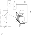
- Fig. 2 shows the general configuration of each of the pixels P along with other circuitry that may or may not be resident in different wafers and thus chip dies of the singulated sensors.
- a count is generated by the Vref controller/counter RC and received through the count driver/tristate buffer TRI. This count is compared to the previous illumination value, held in the old illumination latch array LO, by a digital comparator CX. At the moment the count reaches the stored previous illumination value, the digital comparator signals control logic CL.
- a photoreceptor PR is resident in each of the pixels. It converts the incoming light L into a photoreceptor voltage Vs with either with linear or logarithmic charge to voltage mapping.
- a comparator C of the pixel P compares the photoreceptor voltage Vs with the reference voltage Vref. This comparator may include some form of hysteresis to avoid problems due to bouncing comparator output.
- Vref is a voltage ramp with a threshold offset with respect to a nominal ramp Vnom.
- the Vref ramp has an ON threshold offset (ThrON) and during the threshold OFF event detection phase, the Vref ramp has an OFF threshold offset (ThrOFF) as shown in Fig. 5 .
- the corresponding ON or OFF event is triggered and stored for readout in the event register ER by the control logic CL for either of the threshold ON event detection phase or the threshold OFF event detection phase.
- some embodiments will exploit stacked CIS processes.
- the photoreceptor PR in an upper wafer, will "write" its value into a lower digital wafer, in which memory (old illumination latch array LO) and/or processing (digital comparator CX, control logic CL, event register ER) is performed. Avoiding the use of some or all of the analog memories avoids leakage and in a stacked CIS process; it potentially allows the pixel to be shrunk.
- any portions of analog circuits including PMOS transistors are also implemented in the lower wafer.
- PMOS transistors are in upper wafers.
- two or three PMOS transistors are needed. These can be implemented on lower wafers. This needs two or three wafer-to-wafer connections per pixel depending on the implementation of the amplifier.
- Fig. 3 shows the different phases of the pixels of the sensor.
- step 310 the photoreceptor PR integrates the photocurrent such that the sensor voltage Vs is proportional to the intensity of the received light L, in an exposure phase.
- Vref is set to preferably an exponential ramp plus the ON threshold ThrON. If present, the control logic CL stores an event in the event register ER.
- Vref is set to preferably an exponential ramp plus the OFF threshold ThrOFF. If present, the control logic CL stores an event in the event register ER .
- the thresholds ThrON and ThrOff may be constant during the ramps, or they may vary for different portions of the ramp. If the ramp voltage increases exponentially, it may be beneficial if the thresholds increase exponentially as well.
- the comparator C triggers when the reference voltage Vref exceeds the sensor voltage V, and during this phase, if an event is stored in the event register ER, the control logic CL then clocks the old illumination latch array LO to store the current count as the new illumination value to be held in the latch array.
- the control logic also provides this new illumination value as the pixel's grayscale value.
- the content of the event register ER and illumination latch array LO are provided to indicate an event and the pixel's grayscale value.
- Fig. 4 is a circuit diagram of the pixels P according to a more specific embodiment that uses a level sensitive memory.
- a conventional active pixel circuit (APS) front-end includes a pinned photodiode PD and charge transfer transistor Tx controlled by a charge transfer signal TX, a floating diffusion FD and a reset transistor Trs controlled by a reset signal RS.
- APS active pixel circuit
- the pixel P uses the same comparator C for readout/comparison by providing a feedback path from the output of the comparator C to its inverting input (-).
- a double sampling is inherently used to reduce pixel-to-pixel differences due to comparator offsets.
- the control logic CL includes a multiplexor M that is controlled by a binary signal ON, which is logic high during the threshold ON event detection phase.
- the multiplexor passes the output of the comparator C or its inverse.
- a first AND gate AG1 of the control logic CL receives the output of the multiplexor M, a signal THR that is logic high during both the threshold ON event detection phase and threshold OFF event detection phase along with the output of the digital comparator CX.
- the output of the first AND gate AG1 is received at the set input of a set-reset latch SR. This latch is reset at the end of the registration phase by signal NF.
- the event output is provided through a second AND gate AG2 when signal SEL is high during the readout phase.
- Signal SEL is logic high for each row separately for a short time. There are separate instances: sel 0, sel 1, ... , sel n, for each row of the pixel array.
- a second OR gate OR2 receives the inverted output of the set-reset latch SR, the output of the comparator C and the THR signal. Its inverted output drives the enable inputs of the D latches of the old illumination latch array LO.
- Fig. 5 is a timing diagram showing the signals for the pixel circuit of Fig. 4 .
- Fig. 6 is a circuit diagram of the pixels P according to a second embodiment that also uses a level sensitive memory.
- the output of the multiplexor M is provided to the second OR gate OR2, which also receives a not-output of the set-reset latch SR.
- a pulse-generator is added between OR2 and the enable input E of the memory.
- Fig. 7 is a circuit diagram of the pixels P according to a third embodiment that uses an edge sensitive memory.
- This second set-reset latch SR2 is reset by signal NF that signals the end of the readout phase.
- the output of the multiplexor M is provided to a third AND gate AG3, which also receives a not-output of the set-reset latch SR.
- Fig. 8 is a circuit diagram of the pixels P according to a fourth embodiment.
- a third OR gate OR3 receives the not output of the set-reset latch SR along with an active low row select signal SEL_n enabling row-based readout.
- the active low row select signal SEL_n also controls the old illumination latch array LO via a third AND gate AG3.
- OR1 is inserted between AND gate AG1 and set-reset latch SR.
- An input DRS to this OR gate allows forcing an event in each pixel, which forces the sensor to output grayscale values for each pixel.
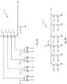
- Fig. 9A is a circuit diagram of one embodiment of the digital comparator CX.
- It includes a series of XOR gates ORC that receive the bits of the count A ⁇ n> and the bits of the old illumination value A ⁇ n> and drive respective PMOS transistors Tc to produce the output OUT.
- Fig. 9B is a circuit diagram of another embodiment of the digital comparator CX.
- NMOS transistor series-connect pairs that receive the bits of the count A ⁇ n> and the bits of the old illumination value B ⁇ n>, respectively. Each pair are in series between an output node OUT and ground.
- a PMOS transistor with the gate connected to a bias voltage implements a current source between the power supply and the output node.
- Fig. 10 shows an alternative front end with an antibloom transistor Ta triggered by an antibloom signal to control the sensitivity of the photodiode PD.
- Anti-bloom transistor prevents photodiode node going below ground, which would turn on Tx transistor.
- Fig. 11 is a block diagram of an exemplary the Vref controller/counter RC.
- the three ramps are each stored in a three separate memory location as lookup table.
- Vref with the ThrON offset for the ON detection phase is stored in memory location 410.
- Vref with the ThrOFF offset for the OFF detection phase is stored in memory location 412.
- Vnom for the registration phase is stored in memory location 412.
- the counter circuit 416 serves as memory address.
- the output of these three memory locations as well as a reset level (is applied to the pixels when signal RS is high) and an idle level (is applied the rest of the time when no ramp and no reset is done) go into the multiplexer 418.
- the output of the multiplexer is connected to the DAC RG.
- An offset may be added to the counter value before the counter value is sent to the array.
- Figs. 12A and 12B show two alternative front end circuits that could be used in place of the previous examples.
- Fig. 12A shows a log feedback arrangement with logarithmic illumination to voltage mapping.
- Fig. 12B shows a photovoltaic arrangement with logarithmic illumination to voltage mapping.
- Figs. 12C and 12D show two further alternative front end circuits that signal to the comparator C.
- Fig. 12C shows a log feedback arrangement wherein the output of the comparator C is feedback through a switch SW3 controlled by the Reset signal. The feedback is received in an amplifier arrangement producing FOut to the comparator C.
- the amplifier comprises transistors T1, T2, T3, T4, where transistor T2 is also controlled by the inverted Reset signal and transistor T3 is controlled by a bias voltage signal.
- Fig. 12D shows a photovoltaic feedback arrangement wherein the output of the comparator C is feedback through switch SW3 controlled by the Reset signal.
- the feedback is received in an amplifier arrangement producing FOut to the comparator C.
- the amplifier comprises transistors T5, and T7.
- Transistor T6 is also controlled by the Reset signal.
- the frontend may also be implemented using logarithmic frontends which results in an increased noise due to the absence of double sampling schemes, mismatch and continuous time operation. If a front-end with logarithmic light to voltage mapping is used, then Vref ramp and counter output should be both linear.
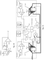
- Fig. 13 shows the lay-out of an event-based vision sensor EBVS employing multiple voltage ramps for ON event, OFF event, and grayscale detection that uses a subpixel scheme.
Landscapes
- Engineering & Computer Science (AREA)
- Multimedia (AREA)
- Signal Processing (AREA)
- Transforming Light Signals Into Electric Signals (AREA)
Claims (8)
- Optischer Sensor mit einer Vielzahl von Pixeln, wobei jedes Pixel umfasst:einen Photorezeptor (PD), der eingerichtet ist, um während einer Belichtungsphase empfangenes Licht in eine Photorezeptorspannung zu konvertieren;einen Analogkomparator (C), der eingerichtet ist, um während einer Detektierungsphase die Photorezeptorspannung mit einer EIN-Ereignisrampe zum Bestimmen von EIN-Ereignissen, einer AUS-Ereignisrampe zum Bestimmen von AUS-Ereignissen, und einer Registrierungsrampe zum Bestimmen einer aktuellen Beleuchtung des Photorezeptors zu vergleichen, wobei die EIN-Ereignisrampe zu der Registrierungsrampe durch einen EIN-Schwellenwertversatz versetzt ist, und die AUS-Ereignisrampe zu der Registrierungsrampe um einen AUS-Schwellenwertversatz in entgegengesetzter Weise versetzt ist, wobei jede der Rampen eine Spannungsrampe ist, deren Spannung im Zeitverlauf zunimmt oder abnimmt, wobei Zählen von Zunahme-/Abnahme-Schritten der Spannungsrampen in digitaler Weise die Werte der Spannungsrampen durch Zählwerte repräsentiert, und eingerichtet ist, um während der Detektierungsphase den Zählwert der Registrierungsrampe als Registrierungszählwert, wenn die Registrierungsrampe die Photorezeptorspannung erreicht, den Zählwert der EIN-Ereignisrampe als EIN-Zählwert, wenn die EIN-Ereignisrampe die Photorezeptorspannung erreicht, und den Zählwert der AUS-Ereignisrampe als AUS-Zählwert zu generieren, wenn die AUS-Ereignisrampe die Photorezeptorspannung erreicht;einen Speicher (LO), der eingerichtet ist, um den Registrierungszählwert während der Detektierungsphase zu speichern;einen Digitalkomparator (AG1), der eingerichtet ist, um den Registrierungszählwert einer früheren Detektierungsphase und entweder den EIN-Zählwert oder den AUS-Zählwert der aktuellen Detektierungsphase zu vergleichen; undSteuerlogik, die eingerichtet ist, um zu bestimmen, dass ein EIN-Ereignis aufgetreten ist, wenn der EIN-Zählwert der aktuellen Detektierungsphase den Registrierungszählwert der früheren Detektierungsphase erreicht, und um zu bestimmen, dass ein AUS-Ereignis aufgetreten ist, wenn ein AUS-Zählwert der aktuellen Detektierungsphase den Registrierungszählwert der früheren Detektierungsphase erreicht.
- Sensor nach Anspruch 1, wobei der Photorezeptor und mindestens ein Teil des Analogkomparators in einem anderen Wafer als von dem Speicher und dem Digitalkomparator implementiert sind.
- Sensor nach einem der Ansprüche 1 bis 2, wobei der Digitalkomparator mit einem anderen Pixel gemeinsam genutzt wird.
- Sensor nach einem der Ansprüche 1 bis 3, wobei die Rampenspannung im Zeitverlauf exponentiell variiert.
- Optisches Abfühlverfahren, umfassend:während einer Belichtungsphase Konvertieren von empfangenem Licht in eine Photorezeptorspannung mit einem Photorezeptor (PD);während einer Detektierungsphase Vergleichen der Photorezeptorspannung mit einer EIN-Ereignisrampe zum Bestimmen von EIN-Ereignissen, einer AUS-Ereignisrampe zum Bestimmen von AUS-Ereignissen, und einer Registrierungsrampe zum Bestimmen einer aktuellen Beleuchtung des Photorezeptors mit einem Analogkomparator (C), wobei die EIN-Ereignisrampe zu der Registrierungsrampe um einen EIN-Schwellenwertversatz versetzt ist, und die AUS-Ereignisrampe zu der Registrierungsrampe um einen AUS-Schwellenwertversatz in entgegengesetzter Weise versetzt ist, wobei jede der Rampen eine Spannungsrampe ist, deren Spannung im Zeitverlauf zunimmt oder abnimmt, wobei Zählen von Zunahme-/Abnahme-Schritten der Spannungsrampen in digitaler Weise die Werte der Spannungsrampen durch Zählwerte repräsentiert, undwährend der Detektierungsphase Generieren des Zählwerts der Registrierungsrampe als Registrierungszählwert, wenn die Registrierungsrampe die Photorezeptorspannung erreicht, des Zählwerts der EIN-Ereignisrampe als EIN-Zählwert, wenn die EIN-Ereignisrampe die Photorezeptorspannung erreicht, und des Zählwerts der AUS-Ereignisrampe als AUS-Zählwert, wenn die AUS-Ereignisrampe die Photorezeptorspannung erreicht, mit dem Analogkomparator C;Speichern des Registrierungszählwerts in einem Speicher (LO) während der Detektierungsphase;Vergleichen des Registrierungszählwerts einer früheren Detektierungsphase und entweder des EIN-Zählwerts oder des AUS-Zählwerts der aktuellen Detektierungsphase mit einem Digitalkomparator (AG1); undmit Steuerlogik Bestimmen, dass ein EIN-Ereignis aufgetreten ist, wenn der EIN-Zählwert der aktuellen Detektierungsphase den Registrierungszählwert der früheren Detektierungsphase erreicht, und Bestimmen, dass ein AUS-Ereignis aufgetreten ist, wenn der AUS-Zählwert der aktuellen Detektierungsphase den Registrierungszählwert der früheren Detektierungsphase erreicht.
- Verfahren nach Anspruch 5, wobei der Photorezeptor und mindestens ein Teil des Analogkomparators in einem anderen Wafer als von dem Speicher und dem Digitalkomparator implementiert sind.
- Verfahren nach einem der Ansprüche 5 bis 6, des Weiteren umfassend gemeinsames Nutzen des Digitalkomparators zwischen den Pixeln.
- Verfahren nach einem der Ansprüche 5 bis 7, wobei Rampenspannungen im Zeitverlauf exponentiell variieren.
Applications Claiming Priority (2)
| Application Number | Priority Date | Filing Date | Title |
|---|---|---|---|
| US201962846283P | 2019-05-10 | 2019-05-10 | |
| PCT/IB2020/054398 WO2020229980A1 (en) | 2019-05-10 | 2020-05-08 | Event-based vision sensor using on/off event and grayscale detection ramps |
Publications (2)
| Publication Number | Publication Date |
|---|---|
| EP3967028A1 EP3967028A1 (de) | 2022-03-16 |
| EP3967028B1 true EP3967028B1 (de) | 2023-11-01 |
Family
ID=70740713
Family Applications (1)
| Application Number | Title | Priority Date | Filing Date |
|---|---|---|---|
| EP20726550.5A Active EP3967028B1 (de) | 2019-05-10 | 2020-05-08 | Ereignisbasierter sichtsensor mit verwendung von ein/aus-ereignis und graustufendetektionsrampen |
Country Status (5)
| Country | Link |
|---|---|
| US (1) | US11825229B2 (de) |
| EP (1) | EP3967028B1 (de) |
| KR (1) | KR20220006082A (de) |
| CN (1) | CN113812142B (de) |
| WO (1) | WO2020229980A1 (de) |
Families Citing this family (12)
| Publication number | Priority date | Publication date | Assignee | Title |
|---|---|---|---|---|
| ES2981443T3 (es) | 2019-04-25 | 2024-10-08 | Beijing Ruisizhixin Tech Co Ltd | Sensor de visión delta |
| ES2962472T3 (es) * | 2020-06-26 | 2024-03-19 | Alpsentek Gmbh | Sensor de imagen delta con almacenamiento de píxeles digital |
| DE102020119243A1 (de) * | 2020-07-21 | 2022-01-27 | Vision Components Gesellschaft Für Bildverarbeitungssysteme Mbh | Verfahren und System bzw. Vorrichtung zum Erkennen eines Objektes in einem elektronischen Bild |
| EP3955566B1 (de) | 2020-08-14 | 2023-06-07 | Alpsentek GmbH | Bildsensor mit konfigurierbarer pixelschaltung und verfahren |
| CN113365004B (zh) * | 2021-06-07 | 2022-03-29 | 豪威芯仑传感器(上海)有限公司 | 一种像素采集电路及图像传感器 |
| CN114095676B (zh) * | 2021-11-23 | 2025-01-10 | 深圳锐视智芯科技有限公司 | 一种带数字像素存储的差量图像传感器 |
| EP4372862A4 (de) | 2022-01-14 | 2025-06-04 | LG Energy Solution, Ltd. | Verfahren zur herstellung einer gelpolymerelektrolyt-sekundärbatterie und gelpolymerelektrolyt-sekundärbatterie daraus |
| US20230243927A1 (en) * | 2022-02-03 | 2023-08-03 | Optex Co., Ltd. | Distance measuring device, automatic door system, opening-closing system, and distance measurement method |
| CN114500868B (zh) * | 2022-04-18 | 2022-07-12 | 深圳锐视智芯科技有限公司 | 一种evs像素工作方法及相关装置 |
| CN116054831B (zh) * | 2022-12-15 | 2025-07-11 | 重庆中星微人工智能芯片技术有限公司 | 一种双斜率模拟数字转换器及模拟数字转换的方法 |
| KR20250011007A (ko) | 2023-07-13 | 2025-01-21 | 삼성전자주식회사 | 바이어스 가변 회로를 포함하는 다이나믹 비전 센서, 이미지 처리 프로세서 및 어플리케이션 프로세서 |
| CN119854650B (zh) * | 2024-12-23 | 2025-12-19 | 华中科技大学 | 一种用于融合型视觉传感器的自适应曝光电路 |
Family Cites Families (7)
| Publication number | Priority date | Publication date | Assignee | Title |
|---|---|---|---|---|
| KR101331982B1 (ko) | 2005-06-03 | 2013-11-25 | 우니페르지타에트 취리히 | 시간 의존적 이미지 데이터를 검출하기 위한 광 어레이 |
| WO2008060124A2 (en) * | 2006-11-17 | 2008-05-22 | Silicon Communications Technology Co., Ltd. | Low power image sensor adjusting reference voltage automatically and optical pointing device comprising the same |
| JP2010251957A (ja) * | 2009-04-14 | 2010-11-04 | Sony Corp | Ad変換装置、固体撮像素子、およびカメラシステム |
| JP6029286B2 (ja) * | 2012-02-17 | 2016-11-24 | キヤノン株式会社 | 光電変換装置および撮像システム |
| TWI659652B (zh) * | 2013-08-05 | 2019-05-11 | 新力股份有限公司 | 攝像裝置、電子機器 |
| WO2018122798A1 (en) | 2016-12-30 | 2018-07-05 | Insightness Ag | Dynamic vision sensor architecture |
| US11082656B2 (en) * | 2017-10-30 | 2021-08-03 | Sony Semiconductor Solutions Corporation | Solid-state imaging device |
-
2020
- 2020-05-08 WO PCT/IB2020/054398 patent/WO2020229980A1/en not_active Ceased
- 2020-05-08 EP EP20726550.5A patent/EP3967028B1/de active Active
- 2020-05-08 US US17/609,439 patent/US11825229B2/en active Active
- 2020-05-08 KR KR1020217038779A patent/KR20220006082A/ko not_active Withdrawn
- 2020-05-08 CN CN202080034755.7A patent/CN113812142B/zh active Active
Also Published As
| Publication number | Publication date |
|---|---|
| US11825229B2 (en) | 2023-11-21 |
| WO2020229980A1 (en) | 2020-11-19 |
| KR20220006082A (ko) | 2022-01-14 |
| CN113812142B (zh) | 2024-10-15 |
| EP3967028A1 (de) | 2022-03-16 |
| US20220224856A1 (en) | 2022-07-14 |
| CN113812142A (zh) | 2021-12-17 |
Similar Documents
| Publication | Publication Date | Title |
|---|---|---|
| EP3967028B1 (de) | Ereignisbasierter sichtsensor mit verwendung von ein/aus-ereignis und graustufendetektionsrampen | |
| EP3967027B1 (de) | Dynamischer bildsensor mit digitaler veränderungserkennung in einem pixel | |
| JP7374242B2 (ja) | 動的ビジョンセンサアーキテクチャ | |
| US11979673B2 (en) | Image sensor with a plurality of super-pixels | |
| US6762401B2 (en) | CMOS image sensor capable of increasing fill factor and driving method thereof | |
| US12058459B2 (en) | NMOS comparator for image sensor pixel | |
| US11785357B2 (en) | Image sensing device operatable in a plurality of modes | |
| CN114365479A (zh) | 基于事件的视觉传感器的延迟均衡 | |
| Niu et al. | High-Speed Trace Detection DROIC for 15μm-Pitch Cryogenic Infrared FPAs | |
| US20260075334A1 (en) | Image sensing device | |
| US20260019720A1 (en) | Image sensing device | |
| US20100225579A1 (en) | Image sensor and optical pointing system | |
| KR20240018345A (ko) | 선택적 멀티플 샘플링을 수행하는 이미지 센서 및 그 동작 방법 |
Legal Events
| Date | Code | Title | Description |
|---|---|---|---|
| STAA | Information on the status of an ep patent application or granted ep patent |
Free format text: STATUS: UNKNOWN |
|
| STAA | Information on the status of an ep patent application or granted ep patent |
Free format text: STATUS: THE INTERNATIONAL PUBLICATION HAS BEEN MADE |
|
| PUAI | Public reference made under article 153(3) epc to a published international application that has entered the european phase |
Free format text: ORIGINAL CODE: 0009012 |
|
| STAA | Information on the status of an ep patent application or granted ep patent |
Free format text: STATUS: REQUEST FOR EXAMINATION WAS MADE |
|
| 17P | Request for examination filed |
Effective date: 20211116 |
|
| AK | Designated contracting states |
Kind code of ref document: A1 Designated state(s): AL AT BE BG CH CY CZ DE DK EE ES FI FR GB GR HR HU IE IS IT LI LT LU LV MC MK MT NL NO PL PT RO RS SE SI SK SM TR |
|
| DAV | Request for validation of the european patent (deleted) | ||
| DAX | Request for extension of the european patent (deleted) | ||
| REG | Reference to a national code |
Ref country code: DE Ref legal event code: R079 Free format text: PREVIOUS MAIN CLASS: H04N0005374500 Ipc: H04N0025470000 Ref document number: 602020020262 Country of ref document: DE |
|
| GRAP | Despatch of communication of intention to grant a patent |
Free format text: ORIGINAL CODE: EPIDOSNIGR1 |
|
| STAA | Information on the status of an ep patent application or granted ep patent |
Free format text: STATUS: GRANT OF PATENT IS INTENDED |
|
| RIC1 | Information provided on ipc code assigned before grant |
Ipc: H04N 25/79 20230101ALI20230503BHEP Ipc: H04N 25/772 20230101ALI20230503BHEP Ipc: H04N 25/47 20230101AFI20230503BHEP |
|
| INTG | Intention to grant announced |
Effective date: 20230525 |
|
| GRAS | Grant fee paid |
Free format text: ORIGINAL CODE: EPIDOSNIGR3 |
|
| GRAA | (expected) grant |
Free format text: ORIGINAL CODE: 0009210 |
|
| STAA | Information on the status of an ep patent application or granted ep patent |
Free format text: STATUS: THE PATENT HAS BEEN GRANTED |
|
| AK | Designated contracting states |
Kind code of ref document: B1 Designated state(s): AL AT BE BG CH CY CZ DE DK EE ES FI FR GB GR HR HU IE IS IT LI LT LU LV MC MK MT NL NO PL PT RO RS SE SI SK SM TR |
|
| REG | Reference to a national code |
Ref country code: GB Ref legal event code: FG4D |
|
| REG | Reference to a national code |
Ref country code: CH Ref legal event code: EP |
|
| REG | Reference to a national code |
Ref country code: IE Ref legal event code: FG4D |
|
| REG | Reference to a national code |
Ref country code: DE Ref legal event code: R096 Ref document number: 602020020262 Country of ref document: DE |
|
| REG | Reference to a national code |
Ref country code: LT Ref legal event code: MG9D |
|
| REG | Reference to a national code |
Ref country code: NL Ref legal event code: MP Effective date: 20231101 |
|
| PG25 | Lapsed in a contracting state [announced via postgrant information from national office to epo] |
Ref country code: GR Free format text: LAPSE BECAUSE OF FAILURE TO SUBMIT A TRANSLATION OF THE DESCRIPTION OR TO PAY THE FEE WITHIN THE PRESCRIBED TIME-LIMIT Effective date: 20240202 |
|
| PG25 | Lapsed in a contracting state [announced via postgrant information from national office to epo] |
Ref country code: IS Free format text: LAPSE BECAUSE OF FAILURE TO SUBMIT A TRANSLATION OF THE DESCRIPTION OR TO PAY THE FEE WITHIN THE PRESCRIBED TIME-LIMIT Effective date: 20240301 |
|
| PG25 | Lapsed in a contracting state [announced via postgrant information from national office to epo] |
Ref country code: LT Free format text: LAPSE BECAUSE OF FAILURE TO SUBMIT A TRANSLATION OF THE DESCRIPTION OR TO PAY THE FEE WITHIN THE PRESCRIBED TIME-LIMIT Effective date: 20231101 |
|
| REG | Reference to a national code |
Ref country code: AT Ref legal event code: MK05 Ref document number: 1628590 Country of ref document: AT Kind code of ref document: T Effective date: 20231101 |
|
| PG25 | Lapsed in a contracting state [announced via postgrant information from national office to epo] |
Ref country code: NL Free format text: LAPSE BECAUSE OF FAILURE TO SUBMIT A TRANSLATION OF THE DESCRIPTION OR TO PAY THE FEE WITHIN THE PRESCRIBED TIME-LIMIT Effective date: 20231101 |
|
| PG25 | Lapsed in a contracting state [announced via postgrant information from national office to epo] |
Ref country code: AT Free format text: LAPSE BECAUSE OF FAILURE TO SUBMIT A TRANSLATION OF THE DESCRIPTION OR TO PAY THE FEE WITHIN THE PRESCRIBED TIME-LIMIT Effective date: 20231101 |
|
| PG25 | Lapsed in a contracting state [announced via postgrant information from national office to epo] |
Ref country code: ES Free format text: LAPSE BECAUSE OF FAILURE TO SUBMIT A TRANSLATION OF THE DESCRIPTION OR TO PAY THE FEE WITHIN THE PRESCRIBED TIME-LIMIT Effective date: 20231101 |
|
| PG25 | Lapsed in a contracting state [announced via postgrant information from national office to epo] |
Ref country code: NL Free format text: LAPSE BECAUSE OF FAILURE TO SUBMIT A TRANSLATION OF THE DESCRIPTION OR TO PAY THE FEE WITHIN THE PRESCRIBED TIME-LIMIT Effective date: 20231101 Ref country code: LT Free format text: LAPSE BECAUSE OF FAILURE TO SUBMIT A TRANSLATION OF THE DESCRIPTION OR TO PAY THE FEE WITHIN THE PRESCRIBED TIME-LIMIT Effective date: 20231101 Ref country code: IS Free format text: LAPSE BECAUSE OF FAILURE TO SUBMIT A TRANSLATION OF THE DESCRIPTION OR TO PAY THE FEE WITHIN THE PRESCRIBED TIME-LIMIT Effective date: 20240301 Ref country code: GR Free format text: LAPSE BECAUSE OF FAILURE TO SUBMIT A TRANSLATION OF THE DESCRIPTION OR TO PAY THE FEE WITHIN THE PRESCRIBED TIME-LIMIT Effective date: 20240202 Ref country code: ES Free format text: LAPSE BECAUSE OF FAILURE TO SUBMIT A TRANSLATION OF THE DESCRIPTION OR TO PAY THE FEE WITHIN THE PRESCRIBED TIME-LIMIT Effective date: 20231101 Ref country code: BG Free format text: LAPSE BECAUSE OF FAILURE TO SUBMIT A TRANSLATION OF THE DESCRIPTION OR TO PAY THE FEE WITHIN THE PRESCRIBED TIME-LIMIT Effective date: 20240201 Ref country code: AT Free format text: LAPSE BECAUSE OF FAILURE TO SUBMIT A TRANSLATION OF THE DESCRIPTION OR TO PAY THE FEE WITHIN THE PRESCRIBED TIME-LIMIT Effective date: 20231101 Ref country code: PT Free format text: LAPSE BECAUSE OF FAILURE TO SUBMIT A TRANSLATION OF THE DESCRIPTION OR TO PAY THE FEE WITHIN THE PRESCRIBED TIME-LIMIT Effective date: 20240301 |
|
| P01 | Opt-out of the competence of the unified patent court (upc) registered |
Effective date: 20240329 |
|
| PG25 | Lapsed in a contracting state [announced via postgrant information from national office to epo] |
Ref country code: SE Free format text: LAPSE BECAUSE OF FAILURE TO SUBMIT A TRANSLATION OF THE DESCRIPTION OR TO PAY THE FEE WITHIN THE PRESCRIBED TIME-LIMIT Effective date: 20231101 Ref country code: RS Free format text: LAPSE BECAUSE OF FAILURE TO SUBMIT A TRANSLATION OF THE DESCRIPTION OR TO PAY THE FEE WITHIN THE PRESCRIBED TIME-LIMIT Effective date: 20231101 Ref country code: PL Free format text: LAPSE BECAUSE OF FAILURE TO SUBMIT A TRANSLATION OF THE DESCRIPTION OR TO PAY THE FEE WITHIN THE PRESCRIBED TIME-LIMIT Effective date: 20231101 Ref country code: NO Free format text: LAPSE BECAUSE OF FAILURE TO SUBMIT A TRANSLATION OF THE DESCRIPTION OR TO PAY THE FEE WITHIN THE PRESCRIBED TIME-LIMIT Effective date: 20240201 Ref country code: LV Free format text: LAPSE BECAUSE OF FAILURE TO SUBMIT A TRANSLATION OF THE DESCRIPTION OR TO PAY THE FEE WITHIN THE PRESCRIBED TIME-LIMIT Effective date: 20231101 Ref country code: HR Free format text: LAPSE BECAUSE OF FAILURE TO SUBMIT A TRANSLATION OF THE DESCRIPTION OR TO PAY THE FEE WITHIN THE PRESCRIBED TIME-LIMIT Effective date: 20231101 |
|
| PGFP | Annual fee paid to national office [announced via postgrant information from national office to epo] |
Ref country code: DE Payment date: 20240418 Year of fee payment: 5 |
|
| PG25 | Lapsed in a contracting state [announced via postgrant information from national office to epo] |
Ref country code: DK Free format text: LAPSE BECAUSE OF FAILURE TO SUBMIT A TRANSLATION OF THE DESCRIPTION OR TO PAY THE FEE WITHIN THE PRESCRIBED TIME-LIMIT Effective date: 20231101 |
|
| PG25 | Lapsed in a contracting state [announced via postgrant information from national office to epo] |
Ref country code: CZ Free format text: LAPSE BECAUSE OF FAILURE TO SUBMIT A TRANSLATION OF THE DESCRIPTION OR TO PAY THE FEE WITHIN THE PRESCRIBED TIME-LIMIT Effective date: 20231101 |
|
| PG25 | Lapsed in a contracting state [announced via postgrant information from national office to epo] |
Ref country code: SK Free format text: LAPSE BECAUSE OF FAILURE TO SUBMIT A TRANSLATION OF THE DESCRIPTION OR TO PAY THE FEE WITHIN THE PRESCRIBED TIME-LIMIT Effective date: 20231101 |
|
| PG25 | Lapsed in a contracting state [announced via postgrant information from national office to epo] |
Ref country code: SM Free format text: LAPSE BECAUSE OF FAILURE TO SUBMIT A TRANSLATION OF THE DESCRIPTION OR TO PAY THE FEE WITHIN THE PRESCRIBED TIME-LIMIT Effective date: 20231101 Ref country code: SK Free format text: LAPSE BECAUSE OF FAILURE TO SUBMIT A TRANSLATION OF THE DESCRIPTION OR TO PAY THE FEE WITHIN THE PRESCRIBED TIME-LIMIT Effective date: 20231101 Ref country code: IT Free format text: LAPSE BECAUSE OF FAILURE TO SUBMIT A TRANSLATION OF THE DESCRIPTION OR TO PAY THE FEE WITHIN THE PRESCRIBED TIME-LIMIT Effective date: 20231101 Ref country code: EE Free format text: LAPSE BECAUSE OF FAILURE TO SUBMIT A TRANSLATION OF THE DESCRIPTION OR TO PAY THE FEE WITHIN THE PRESCRIBED TIME-LIMIT Effective date: 20231101 Ref country code: DK Free format text: LAPSE BECAUSE OF FAILURE TO SUBMIT A TRANSLATION OF THE DESCRIPTION OR TO PAY THE FEE WITHIN THE PRESCRIBED TIME-LIMIT Effective date: 20231101 Ref country code: CZ Free format text: LAPSE BECAUSE OF FAILURE TO SUBMIT A TRANSLATION OF THE DESCRIPTION OR TO PAY THE FEE WITHIN THE PRESCRIBED TIME-LIMIT Effective date: 20231101 |
|
| REG | Reference to a national code |
Ref country code: DE Ref legal event code: R097 Ref document number: 602020020262 Country of ref document: DE |
|
| PLBE | No opposition filed within time limit |
Free format text: ORIGINAL CODE: 0009261 |
|
| STAA | Information on the status of an ep patent application or granted ep patent |
Free format text: STATUS: NO OPPOSITION FILED WITHIN TIME LIMIT |
|
| 26N | No opposition filed |
Effective date: 20240802 |
|
| PG25 | Lapsed in a contracting state [announced via postgrant information from national office to epo] |
Ref country code: SI Free format text: LAPSE BECAUSE OF FAILURE TO SUBMIT A TRANSLATION OF THE DESCRIPTION OR TO PAY THE FEE WITHIN THE PRESCRIBED TIME-LIMIT Effective date: 20231101 |
|
| PG25 | Lapsed in a contracting state [announced via postgrant information from national office to epo] |
Ref country code: SI Free format text: LAPSE BECAUSE OF FAILURE TO SUBMIT A TRANSLATION OF THE DESCRIPTION OR TO PAY THE FEE WITHIN THE PRESCRIBED TIME-LIMIT Effective date: 20231101 |
|
| REG | Reference to a national code |
Ref country code: CH Ref legal event code: PL |
|
| PG25 | Lapsed in a contracting state [announced via postgrant information from national office to epo] |
Ref country code: MC Free format text: LAPSE BECAUSE OF FAILURE TO SUBMIT A TRANSLATION OF THE DESCRIPTION OR TO PAY THE FEE WITHIN THE PRESCRIBED TIME-LIMIT Effective date: 20231101 |
|
| PG25 | Lapsed in a contracting state [announced via postgrant information from national office to epo] |
Ref country code: LU Free format text: LAPSE BECAUSE OF NON-PAYMENT OF DUE FEES Effective date: 20240508 |
|
| GBPC | Gb: european patent ceased through non-payment of renewal fee |
Effective date: 20240508 |
|
| PG25 | Lapsed in a contracting state [announced via postgrant information from national office to epo] |
Ref country code: MC Free format text: LAPSE BECAUSE OF FAILURE TO SUBMIT A TRANSLATION OF THE DESCRIPTION OR TO PAY THE FEE WITHIN THE PRESCRIBED TIME-LIMIT Effective date: 20231101 Ref country code: LU Free format text: LAPSE BECAUSE OF NON-PAYMENT OF DUE FEES Effective date: 20240508 Ref country code: CH Free format text: LAPSE BECAUSE OF NON-PAYMENT OF DUE FEES Effective date: 20240531 |
|
| REG | Reference to a national code |
Ref country code: BE Ref legal event code: MM Effective date: 20240531 |
|
| PG25 | Lapsed in a contracting state [announced via postgrant information from national office to epo] |
Ref country code: IE Free format text: LAPSE BECAUSE OF NON-PAYMENT OF DUE FEES Effective date: 20240508 |
|
| PG25 | Lapsed in a contracting state [announced via postgrant information from national office to epo] |
Ref country code: BE Free format text: LAPSE BECAUSE OF NON-PAYMENT OF DUE FEES Effective date: 20240531 |
|
| PG25 | Lapsed in a contracting state [announced via postgrant information from national office to epo] |
Ref country code: FR Free format text: LAPSE BECAUSE OF NON-PAYMENT OF DUE FEES Effective date: 20240531 |
|
| PG25 | Lapsed in a contracting state [announced via postgrant information from national office to epo] |
Ref country code: GB Free format text: LAPSE BECAUSE OF NON-PAYMENT OF DUE FEES Effective date: 20240508 |
|
| PG25 | Lapsed in a contracting state [announced via postgrant information from national office to epo] |
Ref country code: RO Free format text: LAPSE BECAUSE OF FAILURE TO SUBMIT A TRANSLATION OF THE DESCRIPTION OR TO PAY THE FEE WITHIN THE PRESCRIBED TIME-LIMIT Effective date: 20231101 |
|
| PG25 | Lapsed in a contracting state [announced via postgrant information from national office to epo] |
Ref country code: CY Free format text: LAPSE BECAUSE OF FAILURE TO SUBMIT A TRANSLATION OF THE DESCRIPTION OR TO PAY THE FEE WITHIN THE PRESCRIBED TIME-LIMIT; INVALID AB INITIO Effective date: 20200508 |
|
| PG25 | Lapsed in a contracting state [announced via postgrant information from national office to epo] |
Ref country code: HU Free format text: LAPSE BECAUSE OF FAILURE TO SUBMIT A TRANSLATION OF THE DESCRIPTION OR TO PAY THE FEE WITHIN THE PRESCRIBED TIME-LIMIT; INVALID AB INITIO Effective date: 20200508 |
|
| PG25 | Lapsed in a contracting state [announced via postgrant information from national office to epo] |
Ref country code: FI Free format text: LAPSE BECAUSE OF FAILURE TO SUBMIT A TRANSLATION OF THE DESCRIPTION OR TO PAY THE FEE WITHIN THE PRESCRIBED TIME-LIMIT Effective date: 20231101 |
|
| REG | Reference to a national code |
Ref country code: DE Ref legal event code: R119 Ref document number: 602020020262 Country of ref document: DE |
|
| PG25 | Lapsed in a contracting state [announced via postgrant information from national office to epo] |
Ref country code: DE Free format text: LAPSE BECAUSE OF NON-PAYMENT OF DUE FEES Effective date: 20251202 |