EP3965273A1 - Startup control method and system, and voltage spike measurement circuit and method - Google Patents
Startup control method and system, and voltage spike measurement circuit and method Download PDFInfo
- Publication number
- EP3965273A1 EP3965273A1 EP21195303.9A EP21195303A EP3965273A1 EP 3965273 A1 EP3965273 A1 EP 3965273A1 EP 21195303 A EP21195303 A EP 21195303A EP 3965273 A1 EP3965273 A1 EP 3965273A1
- Authority
- EP
- European Patent Office
- Prior art keywords
- spike
- voltage
- driving signal
- measured
- measurement value
- Prior art date
- Legal status (The legal status is an assumption and is not a legal conclusion. Google has not performed a legal analysis and makes no representation as to the accuracy of the status listed.)
- Pending
Links
Images






Classifications
-
- G—PHYSICS
- G01—MEASURING; TESTING
- G01R—MEASURING ELECTRIC VARIABLES; MEASURING MAGNETIC VARIABLES
- G01R19/00—Arrangements for measuring currents or voltages or for indicating presence or sign thereof
- G01R19/04—Measuring peak values or amplitude or envelope of AC or of pulses
-
- H—ELECTRICITY
- H02—GENERATION; CONVERSION OR DISTRIBUTION OF ELECTRIC POWER
- H02M—APPARATUS FOR CONVERSION BETWEEN AC AND AC, BETWEEN AC AND DC, OR BETWEEN DC AND DC, AND FOR USE WITH MAINS OR SIMILAR POWER SUPPLY SYSTEMS; CONVERSION OF DC OR AC INPUT POWER INTO SURGE OUTPUT POWER; CONTROL OR REGULATION THEREOF
- H02M1/00—Details of apparatus for conversion
- H02M1/0003—Details of control, feedback or regulation circuits
- H02M1/0025—Arrangements for modifying reference values, feedback values or error values in the control loop of a converter
-
- H—ELECTRICITY
- H02—GENERATION; CONVERSION OR DISTRIBUTION OF ELECTRIC POWER
- H02M—APPARATUS FOR CONVERSION BETWEEN AC AND AC, BETWEEN AC AND DC, OR BETWEEN DC AND DC, AND FOR USE WITH MAINS OR SIMILAR POWER SUPPLY SYSTEMS; CONVERSION OF DC OR AC INPUT POWER INTO SURGE OUTPUT POWER; CONTROL OR REGULATION THEREOF
- H02M1/00—Details of apparatus for conversion
- H02M1/08—Circuits specially adapted for the generation of control voltages for semiconductor devices incorporated in static converters
- H02M1/088—Circuits specially adapted for the generation of control voltages for semiconductor devices incorporated in static converters for the simultaneous control of series or parallel connected semiconductor devices
-
- H—ELECTRICITY
- H02—GENERATION; CONVERSION OR DISTRIBUTION OF ELECTRIC POWER
- H02M—APPARATUS FOR CONVERSION BETWEEN AC AND AC, BETWEEN AC AND DC, OR BETWEEN DC AND DC, AND FOR USE WITH MAINS OR SIMILAR POWER SUPPLY SYSTEMS; CONVERSION OF DC OR AC INPUT POWER INTO SURGE OUTPUT POWER; CONTROL OR REGULATION THEREOF
- H02M1/00—Details of apparatus for conversion
- H02M1/32—Means for protecting converters other than automatic disconnection
- H02M1/34—Snubber circuits
- H02M1/342—Active non-dissipative snubbers
-
- H—ELECTRICITY
- H02—GENERATION; CONVERSION OR DISTRIBUTION OF ELECTRIC POWER
- H02M—APPARATUS FOR CONVERSION BETWEEN AC AND AC, BETWEEN AC AND DC, OR BETWEEN DC AND DC, AND FOR USE WITH MAINS OR SIMILAR POWER SUPPLY SYSTEMS; CONVERSION OF DC OR AC INPUT POWER INTO SURGE OUTPUT POWER; CONTROL OR REGULATION THEREOF
- H02M1/00—Details of apparatus for conversion
- H02M1/36—Means for starting or stopping converters
-
- H—ELECTRICITY
- H02—GENERATION; CONVERSION OR DISTRIBUTION OF ELECTRIC POWER
- H02M—APPARATUS FOR CONVERSION BETWEEN AC AND AC, BETWEEN AC AND DC, OR BETWEEN DC AND DC, AND FOR USE WITH MAINS OR SIMILAR POWER SUPPLY SYSTEMS; CONVERSION OF DC OR AC INPUT POWER INTO SURGE OUTPUT POWER; CONTROL OR REGULATION THEREOF
- H02M3/00—Conversion of DC power input into DC power output
- H02M3/01—Resonant DC/DC converters
-
- H—ELECTRICITY
- H02—GENERATION; CONVERSION OR DISTRIBUTION OF ELECTRIC POWER
- H02M—APPARATUS FOR CONVERSION BETWEEN AC AND AC, BETWEEN AC AND DC, OR BETWEEN DC AND DC, AND FOR USE WITH MAINS OR SIMILAR POWER SUPPLY SYSTEMS; CONVERSION OF DC OR AC INPUT POWER INTO SURGE OUTPUT POWER; CONTROL OR REGULATION THEREOF
- H02M3/00—Conversion of DC power input into DC power output
- H02M3/22—Conversion of DC power input into DC power output with intermediate conversion into AC
- H02M3/24—Conversion of DC power input into DC power output with intermediate conversion into AC by static converters
- H02M3/28—Conversion of DC power input into DC power output with intermediate conversion into AC by static converters using discharge tubes with control electrode or semiconductor devices with control electrode to produce the intermediate AC
- H02M3/325—Conversion of DC power input into DC power output with intermediate conversion into AC by static converters using discharge tubes with control electrode or semiconductor devices with control electrode to produce the intermediate AC using devices of a triode or a transistor type requiring continuous application of a control signal
- H02M3/335—Conversion of DC power input into DC power output with intermediate conversion into AC by static converters using discharge tubes with control electrode or semiconductor devices with control electrode to produce the intermediate AC using devices of a triode or a transistor type requiring continuous application of a control signal using semiconductor devices only
- H02M3/33569—Conversion of DC power input into DC power output with intermediate conversion into AC by static converters using discharge tubes with control electrode or semiconductor devices with control electrode to produce the intermediate AC using devices of a triode or a transistor type requiring continuous application of a control signal using semiconductor devices only having several active switching elements
- H02M3/33573—Full-bridge at primary side of an isolation transformer
-
- H—ELECTRICITY
- H02—GENERATION; CONVERSION OR DISTRIBUTION OF ELECTRIC POWER
- H02M—APPARATUS FOR CONVERSION BETWEEN AC AND AC, BETWEEN AC AND DC, OR BETWEEN DC AND DC, AND FOR USE WITH MAINS OR SIMILAR POWER SUPPLY SYSTEMS; CONVERSION OF DC OR AC INPUT POWER INTO SURGE OUTPUT POWER; CONTROL OR REGULATION THEREOF
- H02M3/00—Conversion of DC power input into DC power output
- H02M3/22—Conversion of DC power input into DC power output with intermediate conversion into AC
- H02M3/24—Conversion of DC power input into DC power output with intermediate conversion into AC by static converters
- H02M3/28—Conversion of DC power input into DC power output with intermediate conversion into AC by static converters using discharge tubes with control electrode or semiconductor devices with control electrode to produce the intermediate AC
- H02M3/325—Conversion of DC power input into DC power output with intermediate conversion into AC by static converters using discharge tubes with control electrode or semiconductor devices with control electrode to produce the intermediate AC using devices of a triode or a transistor type requiring continuous application of a control signal
- H02M3/335—Conversion of DC power input into DC power output with intermediate conversion into AC by static converters using discharge tubes with control electrode or semiconductor devices with control electrode to produce the intermediate AC using devices of a triode or a transistor type requiring continuous application of a control signal using semiconductor devices only
- H02M3/33569—Conversion of DC power input into DC power output with intermediate conversion into AC by static converters using discharge tubes with control electrode or semiconductor devices with control electrode to produce the intermediate AC using devices of a triode or a transistor type requiring continuous application of a control signal using semiconductor devices only having several active switching elements
- H02M3/33576—Conversion of DC power input into DC power output with intermediate conversion into AC by static converters using discharge tubes with control electrode or semiconductor devices with control electrode to produce the intermediate AC using devices of a triode or a transistor type requiring continuous application of a control signal using semiconductor devices only having several active switching elements having at least one active switching element at the secondary side of an isolation transformer
-
- H—ELECTRICITY
- H02—GENERATION; CONVERSION OR DISTRIBUTION OF ELECTRIC POWER
- H02M—APPARATUS FOR CONVERSION BETWEEN AC AND AC, BETWEEN AC AND DC, OR BETWEEN DC AND DC, AND FOR USE WITH MAINS OR SIMILAR POWER SUPPLY SYSTEMS; CONVERSION OF DC OR AC INPUT POWER INTO SURGE OUTPUT POWER; CONTROL OR REGULATION THEREOF
- H02M3/00—Conversion of DC power input into DC power output
- H02M3/22—Conversion of DC power input into DC power output with intermediate conversion into AC
- H02M3/24—Conversion of DC power input into DC power output with intermediate conversion into AC by static converters
- H02M3/28—Conversion of DC power input into DC power output with intermediate conversion into AC by static converters using discharge tubes with control electrode or semiconductor devices with control electrode to produce the intermediate AC
- H02M3/325—Conversion of DC power input into DC power output with intermediate conversion into AC by static converters using discharge tubes with control electrode or semiconductor devices with control electrode to produce the intermediate AC using devices of a triode or a transistor type requiring continuous application of a control signal
- H02M3/335—Conversion of DC power input into DC power output with intermediate conversion into AC by static converters using discharge tubes with control electrode or semiconductor devices with control electrode to produce the intermediate AC using devices of a triode or a transistor type requiring continuous application of a control signal using semiconductor devices only
- H02M3/33569—Conversion of DC power input into DC power output with intermediate conversion into AC by static converters using discharge tubes with control electrode or semiconductor devices with control electrode to produce the intermediate AC using devices of a triode or a transistor type requiring continuous application of a control signal using semiconductor devices only having several active switching elements
- H02M3/33576—Conversion of DC power input into DC power output with intermediate conversion into AC by static converters using discharge tubes with control electrode or semiconductor devices with control electrode to produce the intermediate AC using devices of a triode or a transistor type requiring continuous application of a control signal using semiconductor devices only having several active switching elements having at least one active switching element at the secondary side of an isolation transformer
- H02M3/33584—Bidirectional converters
-
- Y—GENERAL TAGGING OF NEW TECHNOLOGICAL DEVELOPMENTS; GENERAL TAGGING OF CROSS-SECTIONAL TECHNOLOGIES SPANNING OVER SEVERAL SECTIONS OF THE IPC; TECHNICAL SUBJECTS COVERED BY FORMER USPC CROSS-REFERENCE ART COLLECTIONS [XRACs] AND DIGESTS
- Y02—TECHNOLOGIES OR APPLICATIONS FOR MITIGATION OR ADAPTATION AGAINST CLIMATE CHANGE
- Y02B—CLIMATE CHANGE MITIGATION TECHNOLOGIES RELATED TO BUILDINGS, e.g. HOUSING, HOUSE APPLIANCES OR RELATED END-USER APPLICATIONS
- Y02B70/00—Technologies for an efficient end-user side electric power management and consumption
- Y02B70/10—Technologies improving the efficiency by using switched-mode power supplies [SMPS], i.e. efficient power electronics conversion e.g. power factor correction or reduction of losses in power supplies or efficient standby modes
Definitions
- the disclosure relates to the field of switching power supply, and particularly to a startup control method and system for a DC/DC converter, and a voltage spike measurement circuit and method for a power switch.
- a voltage spike of a power switch is an important consideration, wherein the power switch may be a diode or a Metal-Oxide-Semiconductor Field-Effect Transistor (MOSFET), for example.
- MOSFET Metal-Oxide-Semiconductor Field-Effect Transistor
- the voltage spike shall be less than the maximum allowable working voltage of the power switch with a certain margin. If the voltage spike exceeds the maximum allowable working voltage, the power switch will have a risk of being damaged.
- the switching power supply does not monitor the voltage spike of the power switch in real time. Besides, at the production stage, it is also difficult to test for the voltage spike, so, only a reasonable design can be used to ensure that the voltage spike is below a limit value.
- a high-voltage lithium battery is connected to a high-voltage bus through a relay to supply power for on-board equipment such as a motor driver or a heater.
- on-board equipment such as a motor driver or a heater.
- the bus capacitors shall be charged to a voltage of the lithium battery.
- the on-board DC/DC converter can provide a reverse charging function using the energy of a low-voltage lead-acid battery.
- a low current of the low-voltage side is often set to ensure the voltage spike of the rectifier power switch does not exceed the limit. Therefore, at the startup stage from a low-voltage side to a high-voltage side, the charging power is limited, and the desired charging time is long.
- an active clamping circuit is widely applied to reduce the voltage spike of the rectifier power switch in the converter.
- the clamping capacitor shall be pre-charged to a preset platform voltage.
- the platform voltage equals a secondary voltage obtained by converting a primary voltage of the high-voltage side via a turn ratio of the transformer. If the clamping capacitor has not been pre-charged, or the pre-charge control accuracy is poor, at the beginning of the soft-start, the power switch in the active clamping circuit will have a large current surge, and the rectifier power switch also may have a large voltage spike.
- the disclosure provides a startup control method and system for a DC/DC converter, and a voltage spike measurement circuit and method for a power switch.
- the disclosure provides a startup control method for a DC/DC converter, which is applied to a startup process of the DC/DC converter with energy transferred from a low-voltage side to a high-voltage side, comprising: determining a duty cycle or a frequency of a driving signal according to at least a voltage spike reference value and a voltage spike measurement value of a power switch at the low-voltage side; and outputting the driving signal to the power switch, thereby controlling on and off of the power switch.
- the disclosure further provides a startup control system for a DC/DC converter, which is applied to a startup process of the DC/DC converter with energy transferred from a low-voltage side to a high-voltage side, comprising: a compensator for at least receiving a voltage spike reference value and a voltage spike measurement value of a power switch at the low-voltage side, and outputting a modulation signal at least according to the voltage spike reference value and the voltage spike measurement value; a driving signal generator for receiving the modulation signal and outputting a driving signal, wherein the driving signal is output to the power switch to control on and off of the power switch.
- a startup control system for a DC/DC converter which is applied to a startup process of the DC/DC converter with energy transferred from a low-voltage side to a high-voltage side, comprising: a compensator for at least receiving a voltage spike reference value and a voltage spike measurement value of a power switch at the low-voltage side, and outputting a modulation signal at least according to the voltage spike reference value
- the voltage spike reference value may comprise a first threshold and a second threshold smaller than the first threshold.
- the compensator may be configured to regulate the modulation signal according to relations between the voltage spike measurement value and the first and second thresholds, thereby regulating a duty cycle of the driving signal.
- the compensator regulates the modulation signal to decrease the duty cycle of the driving signal
- the compensator regulates the modulation signal to increase the duty cycle of the driving signal.
- the compensator may be configured to obtain a voltage error according to the voltage spike measurement value and the voltage spike reference value, and regulate the modulation signal according to the voltage error, thereby regulating the duty cycle of the driving signal.
- the compensator regulates the modulation signal to decrease the duty cycle of the driving signal; and when the voltage spike measurement value is less than the voltage spike reference value, the compensator regulates the modulation signal to increase the duty cycle of the driving signal.
- the compensator may be further configured to receive a low-voltage side current reference value and a low-voltage side current measurement value at the low-voltage side, and output the modulation signal according to the voltage spike reference value, the voltage spike measurement value, the low-voltage side current reference value and the low-voltage side current measurement value.
- the compensator may be further configured to: when the voltage spike measurement value is greater than or equal to the voltage spike reference value, reduce the low-voltage side current reference value, then obtain a current error according to the low-voltage side current reference value and the low-voltage side current measurement value, and obtain the modulation signal according to the current error, thereby regulating the duty cycle of the driving signal. And when the low-voltage side current measurement value is greater than or equal to the low-voltage side current reference value, regulate the modulation signal to decrease the duty cycle of the driving signal.
- the startup control system further comprises a voltage spike measurement unit configured to acquire the voltage spike measurement value of the power switch at the low-voltage side.
- the voltage spike reference value may comprise a first threshold and a second threshold smaller than the first threshold
- the compensator may be configured to regulate the modulation signal according to relations between the voltage spike measurement value and the first and second thresholds, thereby regulating a frequency of the driving signal.
- the compensator regulates the modulation signal to increase the frequency of the driving signal; and when the voltage spike measurement value is less than or equal to the second threshold, the compensator regulates the modulation signal to decrease the frequency of the driving signal.
- the compensator may be configured to obtain a voltage error according to the voltage spike measurement value and the voltage spike reference value, and output the modulation signal according to the voltage error, thereby regulating the frequency of the driving signal.
- the compensator regulates the modulation signal to increase the frequency of the driving signal; when the voltage spike measurement value is less than the voltage spike reference value, the compensator regulates the modulation signal to decrease the frequency of the driving signal.
- the DC/DC converter may comprise a primary circuit, a transformer, and a secondary circuit.
- the primary circuit may comprise a high-voltage capacitor, a first bridge arm, and a second bridge arm connected in parallel to a high-voltage DC end.
- a secondary side of the transformer may comprise a first terminal, a second terminal, and a third terminal.
- the secondary circuit may comprise a first power switch, a second power switch, a filter inductor, and a low-voltage capacitor.
- a primary side of the transformer may be connected to a midpoint of the first bridge arm and a midpoint of the second bridge arm, respectively, the first terminal and the third terminal of the transformer may be connected to one end of the low-voltage capacitor and one DC end of the secondary circuit via the first power switch and the second power switch respectively, and the third terminal of the transformer may be connected to the other end of the low-voltage capacitor and the other DC end of the secondary circuit via the filter inductor.
- the disclosure still further provides a startup control method for a DC/DC converter, which is applied to a startup process of the DC/DC converter with energy transferred from a high-voltage side to a low-voltage side, comprising: acquiring a voltage spike measurement value of a power switch at the low-voltage side; determining a duty cycle or a frequency of a driving signal according to the voltage spike measurement value and a preset voltage; and outputting the driving signal to a power switch at the high-voltage side, thereby charging a clamping capacitor of the power switch at the low-voltage side.
- the duty cycle of the driving signal is gradually increased from zero, and when a difference between the voltage spike measurement values obtained in two adjacent samplings is greater than or equal to a first preset voltage, the duty cycle of the driving signal is controlled to be unchanged until the voltage spike measurement value is greater than or equal to a second preset voltage, then the outputting of the driving signal is stopped.
- the disclosure even further provides a startup control system for a DC/DC converter, which is applied to a startup process of the DC/DC converter with energy transferred from a high-voltage side to a low-voltage side, comprising: a microcontroller unit for receiving a voltage spike measurement value of a power switch at the low-voltage side, and determining a duty cycle or a frequency of a driving signal according to the voltage spike measurement value and a preset voltage, wherein the driving signal is configured to control on or off of a power switch at the high-voltage side, thereby charging a clamping capacitor of the power switch at the low-voltage side.
- the duty cycle of the driving signal output from the microcontroller unit nay be gradually increased from zero.
- the microcontroller unit may control the duty cycle of the driving signal to be unchanged until the voltage spike measurement value is greater than or equal to a second preset voltage, then the microcontroller unit may stop outputting the driving signal.
- the startup control system may further comprise a voltage spike measurement unit configured to acquire the voltage spike measurement value of the power switch at the low-voltage side.
- the DC/DC converter may comprise a primary circuit, a transformer, and a secondary circuit.
- the primary circuit may comprise a high-voltage capacitor, a first bridge arm, and a second bridge arm connected in parallel to a high-voltage DC end.
- a secondary side of the transformer may comprise a first terminal, a second terminal, and a third terminal.
- the secondary circuit may comprise a first power switch, a second power switch, a first clamping branch connected in parallel to the first power switch, a second clamping branch connected in parallel to the second power switch, a filter inductor, and a low-voltage capacitor.
- a primary side of the transformer may be connected to a midpoint of the first bridge arm and a midpoint of the second bridge arm, respectively.
- the first terminal and the third terminal may be connected to one end of the low-voltage capacitor and one DC end of the secondary circuit via the first power switch and the second power switch respectively.
- the third terminal may be connected to the other end of the low-voltage capacitor and the other DC end of the secondary circuit via the filter inductor.
- the first clamping branch and the second clamping branch each may comprise a clamping capacitor.
- the disclosure still further provides a voltage spike measurement circuit for a power switch, comprising: a rectifier unit for receiving a voltage signal of a power switch, and outputting a rectified signal; a capacitive divider unit comprising at least two capacitors connected in series, the capacitive divider unit receiving the rectified signal, dividing the rectified signal according to a capacitance ratio of the at least two capacitors, and outputting a divider signal to a digital signal processor to calculate a voltage spike measurement value of the power switch; and a discharge unit connected in parallel to the capacitive divider unit.
- the rectifier unit may comprise a rectifier diode, and the voltage signal of the power switch may be input from an anode of the rectifier diode.
- the capacitive divider unit may comprise a first capacitor and a second capacitor connected in series, and the divider signal may be output from both ends of the second capacitor.
- the discharge unit may comprise two discharge resistors connected in series, and a connection node of the two discharge resistors may be further connected to a connection node of the first capacitor and the second capacitor.
- the discharge unit may comprise at least one discharge resistor.
- the discharge unit may further comprise a first switch connected in series to the discharge resistor, and a control end of the first switch may be further connected to the digital signal processor.
- the disclosure even further provides a voltage spike measurement method for a power switch, comprising: configuring the voltage spike measurement circuit for a power switch; during a turn-off period of the power switch, when a voltage signal of the power switch is reduced from a spike voltage, calculating a voltage spike measurement value of the power switch through the digital signal processor.
- the discharge unit may comprise at least one discharge resistor and a first switch connected in series to the discharge resistor, wherein a control end of the first switch may be further connected to the digital signal processor.
- the voltage spike measurement method may further comprise: turning on the first switch at a first preset time, such that the capacitive divider unit is discharged through the discharge unit; and turning off the first switch at a second preset time.
- the startup control method and system for a DC/DC converter in the disclosure can improve a reverse charging power to the maximum extent and reduce time desired for charging a bus capacitor when started reversely, and can accurately pre-charge the clamping capacitor when started forwardly.
- the voltage spike measurement circuit and measurement method for a power switch in the disclosure detects voltage stress on the power switch through a capacitive divider.
- the capacitive divider has characteristics of fast response speed, low loss, and strong resistance to interference.
- the capacitive divider does not need an additional RC circuit for filter.
- FIG. 1 shows a topology for a DC/DC converter of the disclosure, wherein reverse working refers to the delivery of energy from a low-voltage side (i.e., LV side) to a high-voltage side (i.e., HV side), and forward working refers to the delivery of energy from the high-voltage side (i.e., HV side) to the low-voltage side (i.e., LV side).
- the DC/DC converter includes a transformer T1, a primary circuit electrically connected to a primary side of the transformer T1, and a secondary circuit electrically connected to a secondary side of the transformer T1.
- the primary circuit includes a high-voltage capacitor C1 and two bridge arms electrically connected in parallel to a high-voltage DC end (HV+ terminal and HV-terminal), wherein the two bridge arms includes a first bridge arm formed by a power switch Qp1 and a power switch Qp2 electrically connected in series and a second bridge arm formed by a power switch Qp3 and a power switch Qp4 electrically connected in series, and wherein the two terminals of the primary side of the transformer T1 is connected to a midpoint of the first bridge arm and a midpoint of the second bridge arm respectively.
- the secondary circuit includes a first power switch SR1, a second power switch SR2, a filter inductor L1, and a low-voltage capacitor C2, wherein the secondary side of the transformer T1 includes a first terminal, a second terminal, and a third terminal.
- One end of the first power switch SRI is electrically connected to the first terminal
- one end of the second power switch SR2 is electrically connected to the third terminal
- both the other end of the first power switch SRI and the other end of the second power switch SR2 are electrically connected to a negative end of the low-voltage capacitor C2 and a DC output negative end (LV-) of the secondary circuit
- the second terminal of the secondary side of the transformer T1 is electrically connected to a positive end of the low-voltage capacitor C2 and a DC output positive end (LV+) of the secondary circuit through the filter inductor L1.
- the active clamping circuits (in this embodiment, for example, a clamping branch consisting of a clamping capacitor Cc1 and a switch Pmos1 electrically connected in series, and a clamping branch consisting of a clamping capacitor Cc2 and a switch Pmos2 electrically connected in series) may be electrically connected in parallel to the first power switch SRI and the second power switch SR2, respectively.
- FIG.2 shows waveforms when the DC/DC converter of FIG. 1 is working reversely.
- the high-voltage capacitor C1 includes capacitors inside the DC/DC converter and on a high-voltage bus and has a very large capacitance value. Since a voltage on the capacitor C1 shall be charged from 0V to a voltage value close to a high-voltage lithium battery voltage in a short time, there may be a large current in the low-voltage side line during a reverse startup stage.
- synchronous rectifier power switches i.e., the power switches SRI and SR2 at the low-voltage side
- a large voltage spike occurs at both ends of the synchronous rectifier power switches (e.g., between a drain and a source of the MOSFET).
- the voltage spike of the synchronous rectifier power switch is often slightly greater than a voltage spike of the clamping capacitor.
- a low-voltage side current value that is the current value of the low-voltage side
- the reverse charging capability of the converter is limited.
- a driving signal for secondary power switches (i.e., power switches at the low-voltage side) of the DC/DC converter is defined as a first driving signal
- a driving signal for primary power switches (i.e., power switches at the high-voltage side) of the DC/DC converter is defined as a second driving signal.
- the disclosure provides a startup control method 100 for a DC/DC converter, which is applied to the startup process of the DC/DC converter with energy transferred from the low-voltage side to the high-voltage side, as shown in FIG. 3 .
- the startup control method 100 may include:
- determining a driving signal may include determining either a duty cycle of a first driving signal or a frequency of the first driving signal.
- FIG. 4 shows a closed-loop control block diagram for a DC/DC converter during its reverse startup process according to one embodiment of the disclosure.
- the DC/DC converter of the disclosure utilizes a startup control system including a compensator 111 and a driving signal generator, wherein the driving signal generator may include a ramp signal generator 112 and a comparator 113, for reverse startup of the DC/DC converter from the low-voltage side to the high-voltage side.
- the compensator 111 is configured to receive at least a voltage spike reference value Spike_ref and a voltage spike measurement value Spike_measured of the power switch at the low-voltage side, and output a modulation signal Error_out at least according to the voltage spike reference value Spike ref and the voltage spike measurement value Spike measured.
- the ramp signal generator 112 is configured to output a ramp signal Ramp_out.
- the comparator 113 is configured to receive the modulation signal Error_out and the ramp signal Ramp_out, and output a first driving signal PWM_out, wherein the first driving signal PWM_out is output to the power switch at the low-voltage side, thereby controlling the on and off of the power switch at the low-voltage side and transmitting energy from the low-voltage side to the high-voltage side.
- the ramp signal Ramp_out may be sawtooth waves, triangular waves, or other waves, but the disclosure is not limited thereto.
- the compensator 111 may include inside a P regulator, a PI regulator, a PID regulator, a PIR regulator, or nonlinear regulators, and the specific types may be selected according to actual situations.
- FIG. 5 shows an embodiment of closed-loop control for the DC/DC converter during its reverse startup process.
- the voltage spike reference value Spike_ref includes a first threshold SR_OV (i.e., an overvoltage point) and a second threshold SR_UV (i.e., an under-voltage point), and the first threshold SR_OV is greater than the second threshold SR UV.
- Determining a duty cycle of the first driving signal PWM_out includes: when the voltage spike measurement value Spike_measured is greater than or equal to the first threshold SR_OV, decreasing the duty cycle of the first driving signal PWM_out; when the voltage spike measurement value Spike measured is less than or equal to the second threshold SR UV, increasing the duty cycle of the first driving signal PWM out; when the voltage spike measurement value Spike measured is between the first threshold SR_OV and the second threshold SR UV, holding the duty cycle of the first driving signal PWM_out unchanged, or decreasing or increasing the duty cycle of the first driving signal PWM out, but the disclosure is not limited thereto. Therefore, the compensator 111 in the startup control system of FIG.
- the 4 of the disclosure is configured to: regulate the output modulation signal Error_out to increase or decrease the duty cycle of the first driving signal PWM_out according to the relation between the voltage spike measurement value Spike measured and the voltage spike reference value (including the overvoltage point and the under-voltage point).
- the compensator 111 regulates the modulation signal Error_out to decrease the duty cycle of the first driving signal PWM out
- the compensator 111 regulates the modulation signal Error_out to increase the duty cycle of the first driving signal PWM_out.
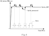
- FIG. 6 shows another embodiment of closed-loop control for the DC/DC converter during its reverse startup process, wherein there is only one reference value.
- Determining the first driving signal PWM_out includes: obtaining a voltage error according to the voltage spike measurement value Spike_measured and the voltage spike reference value Spike ref, obtaining the modulation signal Error_out by inputting the voltage error to a regulator, where the regulator may be a P regulator, a PI regulator, a PID regulator, a PIR regulator or nonlinear regulators, and then obtaining the first driving signal PWM_out according to the modulation signal Error_out.
- the regulation process is as follows: when the voltage spike measurement value Spike_measured is greater than the voltage spike reference value Spike ref, decreasing the duty cycle of the first driving signal PWM_out; and when the voltage spike measurement value Spike_measured is less than the voltage spike reference value Spike ref, increasing the duty cycle of the first driving signal PWM_out.
- 4 may be configured to: regulate the modulation signal Error_out on basis of the voltage error between the voltage spike reference value Spike_ref and the voltage spike measurement value Spike measured, thereby regulating the duty cycle of the first driving signal PWM_out; when the voltage spike measurement value Spike measured is greater than the voltage spike reference value Spike ref, decrease the duty cycle of the first driving signal PWM_out by regulating the modulation signal Error out; and when the voltage spike measurement value Spike measured is less than the voltage spike reference value Spike ref, increase the duty cycle of the first driving signal PWM out by regulating the modulation signal Error_out.
- the voltage spike reference value may be either a constant value or a variable value, such as a value increasing linearly with a specific slope or a stepped-changing value.
- the startup control method 100 may further include determining the duty cycle or the frequency of the first driving signal based on a low-voltage side current reference value and a low-voltage side current measurement value at the low-voltage side.
- FIG. 7 shows a closed-loop control block diagram according to another embodiment of the disclosure when the DC/DC converter is started reversely.
- the compensator 111 is further configured to receive the low-voltage side current reference value iLV_ref and the low-voltage side current measurement value iLV_measured, and output the modulation signal Error_out according to the voltage spike reference value Spike ref, the voltage spike measurement value Spike measured, the low-voltage side current reference value iLV ref, and the low-voltage side current measurement value iLV measured.
- this embodiment adds the low-voltage side current reference value iLV_ref and the low-voltage side current measurement value iLV_measured as inputs to the compensator 111. Therefore, the actual application of the disclosure can be divided into two types: 1. the compensator 111 receives only two variables including the voltage spike reference value Spike_ref and the voltage spike measurement value Spike_measured, and determines the duty cycle or the frequency of the first driving signal PWM_out of the power switch at the low-voltage side according to the two variables. 2.
- the compensator 111 receives four variables including the voltage spike reference value Spike ref, the voltage spike measurement value Spike measured, the low-voltage side current reference value iLV_ref and the low-voltage side current measurement value iLV_measured, and determines the duty cycle or the frequency of the first driving signal PWM_out of the power switch at the low-voltage side according to all the four variables.
- FIG. 8 shows another embodiment of closed-loop control for the DC/DC converter during its reverse startup process.
- determining the duty cycle of the first driving signal includes: when the voltage spike measurement value Spike measured is greater than or equal to the voltage spike reference value Spike ref, reducing the low-voltage side current reference value iLV_ref, thereby decreasing the duty cycle of the first driving signal PWM out.
- a current error is firstly obtained by comparing the low-voltage side current measurement value iLV_measured with the low-voltage side current reference value iLV ref, and then, the current error is inputted to a regulator (such as a P regulator, a PI regulator, or a PIR regulator) to obtain the first driving signal.
- a regulator such as a P regulator, a PI regulator, or a PIR regulator
- the low-voltage side current reference value iLV_ref can be modified according to the voltage spike measurement value and the voltage spike reference value. As the soft-start process tends to its end, the low-voltage side current reference value iLV_ref is linearly reduced as the high-voltage side voltage (the voltage of high-voltage side) rises. If the voltage spike measurement value Spike measured of the power switch at the low-voltage side exceeds the voltage spike reference value Spike_ref, the low-voltage side current reference value iLV_ref is reduced immediately, resulting in that modulation signal Error_out calculated by the compensator 111 changes and the duty cycle of the first driving signal PWM_out decreases eventually.
- the compensator 111 in the startup control system of FIG. 7 of the disclosure may be configured to: when the voltage spike measurement value Spike_measured is greater than or equal to the voltage spike reference value Spike ref, regulate the modulation signal Error_out to decrease the duty cycle of the first driving signal by reducing the low-voltage side current reference value iLV_ref.
- FIG. 9 shows a current-limiting embodiment according to the disclosure when the DC/DC converter is started reversely.
- a low-voltage side overcurrent point iLV_OV i.e., the low-voltage side current reference value
- the duty cycle of the first driving signal is determined, wherein when the low-voltage side current measurement value iLV_measured is greater than or equal to the low-voltage side overcurrent point iLV OV, the duty cycle of the first driving signal is controlled to decrease.
- the working principle of this embodiment is that when the low-voltage side current measurement value iLV_measured is greater than or equal to the preset low-voltage side current reference value (i.e., iLV OV in FIG. 9 ), the duty cycle of the first driving signal is decreased, and when the low-voltage side current measurement value iLV_measured is less than the preset low-voltage side current reference value (i.e., iLV OV in FIG. 9 ), the duty cycle is decided by the voltage spike measurement value and the voltage spike reference value in FIG. 5 or 6 . Therefore, the compensator 111 in the startup control system of FIG. 7 of the disclosure is further configured to: when the low-voltage side current measurement value is greater than or equal to the low-voltage side current reference value, regulate the modulation signal Error_out to decrease the duty cycle of the first driving signal PWM_out.
- the compensator 111 in the startup control system of FIG. 7 of the disclosure is further configured to: when the low-voltage side current measurement value is greater than
- the frequency of the first driving signal when the DC/DC converter is a resonant converter, the frequency of the first driving signal may be determined according to at least the voltage spike measurement value and the voltage spike reference value of the power switch at the low-voltage side.
- different switching frequencies correspond to different gains (i.e., a ratio of the output voltage to the input voltage), so during reverse startup process, the switching frequencies decide currents flowing through the power switches at the low-voltage side, thereby affecting the voltage spike when the power switches are turned off.
- the frequency of the first driving signal can also be controlled by comparing the voltage spike measurement value with the preset voltage spike reference value of the power switch at the low-voltage side.
- the frequency of the first driving signal when the voltage spike measurement value is greater than or equal to the first threshold, the frequency of the first driving signal is increased, and when the voltage spike measurement value is less than or equal to the second threshold, the frequency of the first driving signal is decreased.
- the low-voltage side current may also be limited by taking the low-voltage side current measurement value and the low-voltage side current reference value into consideration, such that the voltage spike of the power switch and the current of the converter are ensured not to exceed a limit during reverse startup process.
- FIG. 10 shows still another closed-loop control block diagram when the DC/DC converter is started reversely according to the disclosure.
- the DC/DC converter of the disclosure can achieve reverse startup from the low-voltage side to the high-voltage side using a startup control system including the compensator 111 and the driving signal generator (including a voltage controlled oscillator 114).
- the compensator 111 is configured to receive the voltage spike reference value Spike_ref and the voltage spike measurement value Spike_measured, or receive the voltage spike reference value Spike ref, the voltage spike measurement value Spike measured, the low-voltage side current reference value iLV ref, and the low-voltage side current measurement value iLV_measured, and output the modulation signal Error_out based on them.
- the voltage controlled oscillator 114 is configured to receive the modulation signal Error_out, and output the first driving signal PWM_out.
- the frequency of the first driving signal PWM_out is determined on basis of the modulation signal Error_out and is sent to the power switch at the low-voltage side, thereby controlling the on or off of the power switch at the low-voltage side, so that the energy can be transmitted from the low-voltage side to the high-voltage side.
- the startup control system of the disclosure may further include a voltage spike measurement unit for acquiring the voltage spike measurement value of the power switch at the low-voltage side.
- the active clamping capacitors Cc1 and Cc2 shall be pre-charged to a voltage value converted from an input voltage at the high-voltage side via a turn ratio of the transformer.
- factors such as device tolerance and environment temperature, such as, delay characteristics of the driver, turn-on and turn-off characteristics of the MOSFET, and capacitance differences of the clamping capacitors, if a difference between a voltage of the clamping capacitors after pre-charging and an expected value is too large, during the soft startup process, the power switches (Pmos1 and Pmos2 shown in FIG. 1 ) within the active clamping circuit may undergo a large current surge, which may result that the spike of the rectifier power switches exceeds a limit.
- the disclosure further provides a startup control method 200 for a DC/DC converter for startup of the DC/DC converter from a high-voltage side to a low-voltage side.
- the startup control method 200 may include:
- determining a driving signal may be determining either a duty cycle or a frequency of a second driving signal.
- the duty cycle of the second driving signal is gradually increased from zero.
- the duty cycle of the second driving signal is controlled to be unchanged till the voltage spike measurement value reaches (i.e., is greater than or equal to) a second preset voltage. Then stop outputting the second driving signal.
- FIG. 12 shows a control block diagram where a clamping capacitor is pre-charged before the DC/DC converter being started forwardly according to the disclosure. It is unnecessary for the DC/DC converter to add an additional pre-charge circuit, thereby pre-charging the clamping capacitor of the power switch at the low-voltage side, and controlling a pre-charge voltage accurately.
- the startup control system of the disclosure includes a microcontroller unit (MCU) 211 for receiving the voltage spike measurement value of the power switch at the low-voltage side, and outputting a second driving signal based on the voltage spike measurement value and a preset voltage, wherein the second driving signal is configured to control the on or off of the power switch at the high-voltage side (e.g., Qp1 to Qp4 shown in FIG. 1 ), thereby charging clamping capacitors (e.g., capacitors Cc1 and Cc2 shown in FIG. 1 ) of the power switch at the low-voltage side.
- MCU microcontroller unit
- the second driving signal may be transmitted to the power switch 213 at the high-voltage side via a driver 212, thereby charging the clamping capacitor 214 of the power switch at the low-voltage side.
- the startup control system may further include a voltage spike measurement unit 215 for acquiring the voltage spike measurement value of the power switch at the low-voltage side that indirectly equivalent to a voltage of the clamping capacitors for feedback control.
- FIG. 13 shows a waveform diagram of one embodiment where the clamping capacitor is pre-charged before the DC/DC converter being started forwardly according to the disclosure.
- FIG. 13 shows the waveform of the second driving signal, the waveform of the actual driving signal output to the power switches at the high-voltage side after the second driving signal passes through the driving chips, and the waveform of the voltage of the clamping capacitor of the power switches at the low-voltage side sequentially from top to bottom.
- the duty cycle of a pulse signal MCU PWM_out i.e., the second driving signal
- a pulse signal MCU PWM_out i.e., the second driving signal
- the power switch at the high-voltage side Due to the narrow width of the pulse signal, the power switch at the high-voltage side is always in an off state, so no energy is delivered to the clamping capacitor of the power switch at the low-voltage side. Subsequently, the duty cycle of the pulse signal MCU PWM_out is gradually increased, such that the power switch at the high-voltage side enters from an off region into a linear region, and the voltage of the clamping capacitor is slightly increased.
- the MCU holds the duty cycle of the pulse signal MCU PWM_out unchanged and charges the clamping capacitor continuously till the voltage spike measurement value reaches a second preset voltage. Then the second driving signal may be closed.
- Such a control method is free from the influence of factors such as parameter difference of the device and temperature change on pre-charge effect, such that consistency of pre-charge results can be ensured.
- the closed-loop pre-charge control method for the active clamping capacitor in the embodiments of the disclosure is not limited to the duty cycle control aforesaid, and may also be frequency control.
- the MCU may timely adjust the frequency of the second driving signal according to the detected voltage spike of the power switch at the low-voltage side.
- the voltage spike measurement value is recognized to begin increasing with a preset extent (i.e., the first preset voltage)
- the frequency of the second driving signal is fixed. Once the voltage spike measurement value reaches a second preset voltage, stop sending the second driving signal.
- the startup control method of the disclosure is not only applicable to the circuit structure shown in FIG. 1 .
- a primary circuit of the DC/DC converter may be a half-bridge structure, and a secondary circuit may be a full-bridge structure.
- the DC/DC converter may be in a resonant topological structure such as LLC or CLLC, but the disclosure is not limited thereto.
- a voltage spike measurement circuit for the power switch in the disclosure mainly includes a rectifier unit 191, a capacitive divider unit 192, and a discharge unit 194.
- the rectifier unit 191 receives a voltage signal Vswitch at both ends of a power switch and outputs a rectified signal.
- the capacitive divider unit 192 includes at least two capacitors connected in series, and the capacitive divider unit 192 receives the rectified signal, divides the rectified signal based on a capacitance ratio of the capacitors, and outputs a divider signal to a digital signal processor (DSP) 193, for example, to calculate a voltage spike measurement value of the power switch.
- DSP digital signal processor
- the discharge unit 194 is connected in parallel to the capacitive divider unit 192.
- the voltage signal may be a voltage signal of the power switch SRI and/or a voltage signal of the power switch SR2 in FIG. 1 .
- the rectifier unit 191 may include, for example, a rectifier diode Dd, and the voltage signal Vswitch at both ends of the power switch is input from an anode of the rectifier diode Dd.
- the rectifier unit 191 can extract and transmit a voltage spike of the power switch to the capacitive divider unit 192.
- the capacitive divider unit 192 may include, for example, a first capacitor Cd1 and a second capacitor Cd2 connected in series, and the divider signal is output from both ends of the second capacitor Cd2.
- the capacitive divider unit 192 can hold the voltage spike of the power switch using the capacitors and divides the voltage spike according to the capacitance ratio to obtain the divider signal receivable by a controller.
- the number of capacitors may be selected according to actual situations.
- the discharge unit 194 may be the structures as shown in FIGS. 15 , 17 , and 19 , but the disclosure is not limited thereto.
- FIG. 15 shows a preferable embodiment of the voltage spike measurement circuit for the power switch according to the disclosure.
- the discharge unit 194 includes a first switch Qnmos connected in series to a discharge resistor Rd, and a control end of the first switch Qnmos is further connected to the digital signal processor DSP.
- the first capacitor Cd1 and the second capacitor Cd2 are preferably C0G ceramic capacitors, with a preferable initial tolerance of 1% or 5%.
- FIG. 16 shows working waveforms in the embodiment of FIG. 15 .
- stage D the voltages of the first capacitor Cd1 and the second capacitor Cd2 are held unchanged because of the cut-off of the discharge circuit.
- the voltages of the first capacitor Cd1 and the second capacitor Cd2 can rise from a relatively high platform voltage to the voltage spike Spike point when the power switch is turned off next time, i.e., during the next voltage spike measurement process, thereby shortening the measurement time.
- a proportional coefficient of the first capacitor Cd1 and the second capacitor Cd2 may be corrected.
- the DSP calculates the sum of voltages of the first capacitor Cd1 and the second capacitor Cd2 by detecting the voltage value of the second capacitor Cd2 and then calculates a platform voltage measurement value at the low-voltage side. Meanwhile, if the switching power supply has an accurate high voltage-side voltage measurement circuit inside, a platform voltage actual value at the low-voltage side can be calculated, and then the proportional coefficient of the first capacitor Cd1 and the second capacitor Cd2 is corrected on basis of the platform voltage measurement value and the platform voltage actual value at the low-voltage side.
- FIG. 17 shows another preferable embodiment of the voltage spike measurement circuit for the power switch according to the disclosure.
- the discharge unit 194 includes two discharge resistors Rd1 and Rd2 connected in series, and a connection node of the two discharge resistors Rd1 and Rd2 is further connected to a connection node of the first capacitor Cd1 and the second capacitor Cd2.
- the first capacitor Cd1 and the second capacitor Cd2 are preferably C0G ceramic capacitors, with a preferable initial tolerance of 1% or 5%, and a preferable tolerance of the two discharge resistors is 1%.
- a measurement error due to the tolerance of the first capacitor Cd1 and the second capacitor Cd2 can be balanced by selecting discharge resistors with high accuracy, thereby improving measurement accuracy.
- FIG. 18 shows working waveforms in the embodiment of FIG. 17 .
- stage A when the voltage Vswitch of the power switch exceeds a sum of voltages of the first capacitor Cd1 and the second capacitor Cd2 connected in series, the first capacitor Cd1 and the second capacitor Cd2 are charged through the diode Dd.
- the diode Dd is reverse cut-off.
- stage B the first capacitor Cd1, and the second capacitor Cd2 are discharged by discharge resistors Rd1 and Rd2.
- the DSP can detect a voltage value of the second capacitor Cd2 at an initial time of stage B, and then calculates the sum of voltages of the first capacitor Cd1 and the second capacitor Cd2 through a relation of the capacitance ratio of the first capacitor Cd1 and the second capacitor Cd2, and the value is proximate to the voltage spike value Spike point of the power switch.
- stage C the first capacitor Cd1, and the second capacitor Cd2 are continuously discharged by the discharge resistors Rd1 and Rd2.
- the embodiment of FIG. 17 cannot correct the proportional coefficient of the first capacitor Cd1 and the second capacitor Cd2. Therefore, an initial deviation and temperature drift characteristics of the first capacitor Cd1 and the second capacitor Cd2 and discharge effect of the discharge resistors Rd1 and Rd2 may influence the accuracy of measurement results of the voltage spike in the embodiment of FIG. 17 .
- the discharge resistors Rd1 and Rd2 may be selected to be with a small tolerance, such as accuracy of +/-0.1%, and an initial deviation of the first capacitor Cd1 and the second capacitor Cd2 can be compensated by reducing resistances of the discharge resistors Rd1 and Rd2 appropriately, thereby obtaining accurate voltage spike measurement values.
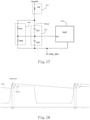
- FIG. 19 shows another preferable embodiment of the voltage spike measurement circuit for a power switch according to the disclosure.
- the discharge unit 194 includes a discharge resistor Rd.
- the first capacitor Cd1 and the second capacitor Cd2 are preferably C0G ceramic capacitors, with a preferable initial tolerance of 1% or 5%.
- FIG. 20 shows working waveforms in the embodiment of FIG. 19 .
- the embodiment of FIG. 19 cannot correct the proportional coefficient of the first capacitor Cd1 and the second capacitor Cd2. Therefore, an initial deviation and temperature drift characteristics of the first capacitor Cd1 and the second capacitor Cd2 and discharge effect of the discharge resistor Rd influence accuracy of measurement results of the voltage spike in the embodiment of FIG. 19 .
- the disclosure further provides a voltage spike measurement method 300 for a power switch, mainly including:
- the voltage spike measurement method 300 for a power switch may further include: turning on the first switch Qnmos at a first preset time, such that the capacitive divider unit 192 is discharged through the discharge unit 194; and turning off the first switch Qnmos at a second preset time, thereby preventing the discharge unit 194 from discharging the capacitive divider unit 192, and holding a high platform voltage on the capacitive divider unit 192.
Landscapes
- Engineering & Computer Science (AREA)
- Power Engineering (AREA)
- Physics & Mathematics (AREA)
- General Physics & Mathematics (AREA)
- Dc-Dc Converters (AREA)
- Electronic Switches (AREA)
Abstract
Description
- The disclosure relates to the field of switching power supply, and particularly to a startup control method and system for a DC/DC converter, and a voltage spike measurement circuit and method for a power switch.
- In the switching power supply, a voltage spike of a power switch is an important consideration, wherein the power switch may be a diode or a Metal-Oxide-Semiconductor Field-Effect Transistor (MOSFET), for example. Generally, the voltage spike shall be less than the maximum allowable working voltage of the power switch with a certain margin. If the voltage spike exceeds the maximum allowable working voltage, the power switch will have a risk of being damaged. Generally speaking, the switching power supply does not monitor the voltage spike of the power switch in real time. Besides, at the production stage, it is also difficult to test for the voltage spike, so, only a reasonable design can be used to ensure that the voltage spike is below a limit value.
- As for the application of electric vehicles, a high-voltage lithium battery is connected to a high-voltage bus through a relay to supply power for on-board equipment such as a motor driver or a heater. Generally, a large number of bus capacitors are connected across the positive and negative poles of the high-voltage bus. Therefore, before the relay is connected, the bus capacitors shall be charged to a voltage of the lithium battery. The on-board DC/DC converter can provide a reverse charging function using the energy of a low-voltage lead-acid battery. When the bus capacitors are charged, a large current of the low-voltage side results in a large voltage spike of the rectifier power switches (power switches at the low-voltage side). In the design phase, a low current of the low-voltage side is often set to ensure the voltage spike of the rectifier power switch does not exceed the limit. Therefore, at the startup stage from a low-voltage side to a high-voltage side, the charging power is limited, and the desired charging time is long.
- Besides, with the improvement of the power density, an active clamping circuit is widely applied to reduce the voltage spike of the rectifier power switch in the converter. Generally, before an output voltage is slowly increased, the clamping capacitor shall be pre-charged to a preset platform voltage. Generally, the platform voltage equals a secondary voltage obtained by converting a primary voltage of the high-voltage side via a turn ratio of the transformer. If the clamping capacitor has not been pre-charged, or the pre-charge control accuracy is poor, at the beginning of the soft-start, the power switch in the active clamping circuit will have a large current surge, and the rectifier power switch also may have a large voltage spike.
- Therefore, it is urgent to develop a new startup control method for a DC/DC converter, which can largely improve startup efficiency and shorten startup time, while ensuring the voltage stress on the power switch does not exceed a limit.
- The disclosure provides a startup control method and system for a DC/DC converter, and a voltage spike measurement circuit and method for a power switch.
- In one aspect, the disclosure provides a startup control method for a DC/DC converter, which is applied to a startup process of the DC/DC converter with energy transferred from a low-voltage side to a high-voltage side, comprising: determining a duty cycle or a frequency of a driving signal according to at least a voltage spike reference value and a voltage spike measurement value of a power switch at the low-voltage side; and outputting the driving signal to the power switch, thereby controlling on and off of the power switch.
- In another aspect, the disclosure further provides a startup control system for a DC/DC converter, which is applied to a startup process of the DC/DC converter with energy transferred from a low-voltage side to a high-voltage side, comprising: a compensator for at least receiving a voltage spike reference value and a voltage spike measurement value of a power switch at the low-voltage side, and outputting a modulation signal at least according to the voltage spike reference value and the voltage spike measurement value; a driving signal generator for receiving the modulation signal and outputting a driving signal, wherein the driving signal is output to the power switch to control on and off of the power switch.
- In one embodiment of the invention, the voltage spike reference value may comprise a first threshold and a second threshold smaller than the first threshold. The compensator may be configured to regulate the modulation signal according to relations between the voltage spike measurement value and the first and second thresholds, thereby regulating a duty cycle of the driving signal. When the voltage spike measurement value is greater than or equal to the first threshold, the compensator regulates the modulation signal to decrease the duty cycle of the driving signal, and when the voltage spike measurement value is less than or equal to the second threshold, the compensator regulates the modulation signal to increase the duty cycle of the driving signal.
- In one embodiment of the invention, the compensator may be configured to obtain a voltage error according to the voltage spike measurement value and the voltage spike reference value, and regulate the modulation signal according to the voltage error, thereby regulating the duty cycle of the driving signal. When the voltage spike measurement value is greater than the voltage spike reference value, the compensator regulates the modulation signal to decrease the duty cycle of the driving signal; and when the voltage spike measurement value is less than the voltage spike reference value, the compensator regulates the modulation signal to increase the duty cycle of the driving signal.
- In one embodiment of the invention, the compensator may be further configured to receive a low-voltage side current reference value and a low-voltage side current measurement value at the low-voltage side, and output the modulation signal according to the voltage spike reference value, the voltage spike measurement value, the low-voltage side current reference value and the low-voltage side current measurement value.
- In one embodiment of the invention, the compensator may be further configured to: when the voltage spike measurement value is greater than or equal to the voltage spike reference value, reduce the low-voltage side current reference value, then obtain a current error according to the low-voltage side current reference value and the low-voltage side current measurement value, and obtain the modulation signal according to the current error, thereby regulating the duty cycle of the driving signal. And when the low-voltage side current measurement value is greater than or equal to the low-voltage side current reference value, regulate the modulation signal to decrease the duty cycle of the driving signal.
- In one embodiment of the invention, the startup control system further comprises a voltage spike measurement unit configured to acquire the voltage spike measurement value of the power switch at the low-voltage side.
- In one embodiment of the invention, the voltage spike reference value may comprise a first threshold and a second threshold smaller than the first threshold, and the compensator may be configured to regulate the modulation signal according to relations between the voltage spike measurement value and the first and second thresholds, thereby regulating a frequency of the driving signal. When the voltage spike measurement value is greater than or equal to the first threshold, the compensator regulates the modulation signal to increase the frequency of the driving signal; and when the voltage spike measurement value is less than or equal to the second threshold, the compensator regulates the modulation signal to decrease the frequency of the driving signal.
- In one embodiment of the invention, the compensator may be configured to obtain a voltage error according to the voltage spike measurement value and the voltage spike reference value, and output the modulation signal according to the voltage error, thereby regulating the frequency of the driving signal. When the voltage spike measurement value is greater than the voltage spike reference value, the compensator regulates the modulation signal to increase the frequency of the driving signal; when the voltage spike measurement value is less than the voltage spike reference value, the compensator regulates the modulation signal to decrease the frequency of the driving signal.
- In one embodiment of the invention, the DC/DC converter may comprise a primary circuit, a transformer, and a secondary circuit. The primary circuit may comprise a high-voltage capacitor, a first bridge arm, and a second bridge arm connected in parallel to a high-voltage DC end. A secondary side of the transformer may comprise a first terminal, a second terminal, and a third terminal. The secondary circuit may comprise a first power switch, a second power switch, a filter inductor, and a low-voltage capacitor. A primary side of the transformer may be connected to a midpoint of the first bridge arm and a midpoint of the second bridge arm, respectively, the first terminal and the third terminal of the transformer may be connected to one end of the low-voltage capacitor and one DC end of the secondary circuit via the first power switch and the second power switch respectively, and the third terminal of the transformer may be connected to the other end of the low-voltage capacitor and the other DC end of the secondary circuit via the filter inductor.
- In another aspect, the disclosure still further provides a startup control method for a DC/DC converter, which is applied to a startup process of the DC/DC converter with energy transferred from a high-voltage side to a low-voltage side, comprising: acquiring a voltage spike measurement value of a power switch at the low-voltage side; determining a duty cycle or a frequency of a driving signal according to the voltage spike measurement value and a preset voltage; and outputting the driving signal to a power switch at the high-voltage side, thereby charging a clamping capacitor of the power switch at the low-voltage side. In one embodiment of the invention, the duty cycle of the driving signal is gradually increased from zero, and when a difference between the voltage spike measurement values obtained in two adjacent samplings is greater than or equal to a first preset voltage, the duty cycle of the driving signal is controlled to be unchanged until the voltage spike measurement value is greater than or equal to a second preset voltage, then the outputting of the driving signal is stopped.
- In another aspect, the disclosure even further provides a startup control system for a DC/DC converter, which is applied to a startup process of the DC/DC converter with energy transferred from a high-voltage side to a low-voltage side, comprising: a microcontroller unit for receiving a voltage spike measurement value of a power switch at the low-voltage side, and determining a duty cycle or a frequency of a driving signal according to the voltage spike measurement value and a preset voltage, wherein the driving signal is configured to control on or off of a power switch at the high-voltage side, thereby charging a clamping capacitor of the power switch at the low-voltage side.
- In one embodiment of the invention, the duty cycle of the driving signal output from the microcontroller unit nay be gradually increased from zero. When a difference between the voltage spike measurement values obtained in two adjacent samplings is greater than or equal to a first preset voltage, the microcontroller unit may control the duty cycle of the driving signal to be unchanged until the voltage spike measurement value is greater than or equal to a second preset voltage, then the microcontroller unit may stop outputting the driving signal.
- In one embodiment of the invention, the startup control system may further comprise a voltage spike measurement unit configured to acquire the voltage spike measurement value of the power switch at the low-voltage side.
- In one embodiment of the invention, the DC/DC converter may comprise a primary circuit, a transformer, and a secondary circuit. The primary circuit may comprise a high-voltage capacitor, a first bridge arm, and a second bridge arm connected in parallel to a high-voltage DC end. A secondary side of the transformer may comprise a first terminal, a second terminal, and a third terminal. The secondary circuit may comprise a first power switch, a second power switch, a first clamping branch connected in parallel to the first power switch, a second clamping branch connected in parallel to the second power switch, a filter inductor, and a low-voltage capacitor. A primary side of the transformer may be connected to a midpoint of the first bridge arm and a midpoint of the second bridge arm, respectively. The first terminal and the third terminal may be connected to one end of the low-voltage capacitor and one DC end of the secondary circuit via the first power switch and the second power switch respectively. The third terminal may be connected to the other end of the low-voltage capacitor and the other DC end of the secondary circuit via the filter inductor. The first clamping branch and the second clamping branch each may comprise a clamping capacitor.
- In another aspect, the disclosure still further provides a voltage spike measurement circuit for a power switch, comprising: a rectifier unit for receiving a voltage signal of a power switch, and outputting a rectified signal; a capacitive divider unit comprising at least two capacitors connected in series, the capacitive divider unit receiving the rectified signal, dividing the rectified signal according to a capacitance ratio of the at least two capacitors, and outputting a divider signal to a digital signal processor to calculate a voltage spike measurement value of the power switch; and a discharge unit connected in parallel to the capacitive divider unit.
- In one embodiment of the invention, the rectifier unit may comprise a rectifier diode, and the voltage signal of the power switch may be input from an anode of the rectifier diode.
- In one embodiment of the invention, the capacitive divider unit may comprise a first capacitor and a second capacitor connected in series, and the divider signal may be output from both ends of the second capacitor.
- In one embodiment of the invention, the discharge unit may comprise two discharge resistors connected in series, and a connection node of the two discharge resistors may be further connected to a connection node of the first capacitor and the second capacitor.
- In one embodiment of the invention, the discharge unit may comprise at least one discharge resistor.
- In one embodiment of the invention, the discharge unit may further comprise a first switch connected in series to the discharge resistor, and a control end of the first switch may be further connected to the digital signal processor.
- In another aspect, the disclosure even further provides a voltage spike measurement method for a power switch, comprising: configuring the voltage spike measurement circuit for a power switch; during a turn-off period of the power switch, when a voltage signal of the power switch is reduced from a spike voltage, calculating a voltage spike measurement value of the power switch through the digital signal processor.
- In one embodiment of the invention, the discharge unit may comprise at least one discharge resistor and a first switch connected in series to the discharge resistor, wherein a control end of the first switch may be further connected to the digital signal processor. The voltage spike measurement method may further comprise: turning on the first switch at a first preset time, such that the capacitive divider unit is discharged through the discharge unit; and turning off the first switch at a second preset time.
- On the premise of ensuring voltage stress on the power switch not to exceed a limit, the startup control method and system for a DC/DC converter in the disclosure can improve a reverse charging power to the maximum extent and reduce time desired for charging a bus capacitor when started reversely, and can accurately pre-charge the clamping capacitor when started forwardly.
- The voltage spike measurement circuit and measurement method for a power switch in the disclosure detects voltage stress on the power switch through a capacitive divider. As compared to the traditional resistance voltage divider, the capacitive divider has characteristics of fast response speed, low loss, and strong resistance to interference. In the disclosure, by dividing the voltage at both ends of the power switch based on a relation of the capacitance ratio then sending the dividing signal to a digital signal processor for measurement, the capacitive divider does not need an additional RC circuit for filter.
- The additional aspects and advantages of the disclosure are partially explained in the below description, and partially apparent from the description, or can be obtained through the practice of the disclosure.
- The exemplary embodiments will be described in detail with reference to the accompanying drawings, through which the above and other features and advantages of the disclosure will become more apparent.
-
FIG. 1 is a topological diagram of a DC/DC converter according to the disclosure. -
FIG. 2 is a waveform diagram of devices when the topology ofFIG. 1 works reversely (with power transferred from a low-voltage side to a high-voltage side). -
FIG. 3 is a flow diagram of a startup control method when the DC/DC converter is started reversely from a low-voltage side to a high-voltage side according to the disclosure. -
FIG. 4 is a closed-loop control block diagram when the DC/DC converter is started reversely according to the disclosure. -
FIG. 5 shows a closed-loop control embodiment when the DC/DC converter is started reversely according to the disclosure. -
FIG. 6 shows another closed-loop control embodiment when the DC/DC converter is started reversely according to the disclosure. -
FIG. 7 is another closed-loop control block diagram when the DC/DC converter is started reversely according to the disclosure. -
FIG. 8 shows still another closed-loop control embodiment when the DC/DC converter is started reversely according to the disclosure. -
FIG. 9 shows a current-limiting embodiment when the DC/DC converter is started reversely according to the disclosure. -
FIG. 10 is still another closed-loop control block diagram when the DC/DC converter is started reversely according to the disclosure. -
FIG. 11 is a flow diagram of a startup control method when the DC/DC converter starts forwardly (with power transferred from a high-voltage side to a low-voltage side) according to the disclosure. -
FIG. 12 is a control block diagram where the DC/DC converter pre-charges a clamping capacitor when started forwardly according to the disclosure. -
FIG. 13 is a waveform diagram of one embodiment where the DC/DC converter pre-charges the clamping capacitor when started forwardly according to the disclosure. -
FIG. 14 is a block diagram of a voltage spike measurement circuit for a power switch according to the disclosure. -
FIG. 15 shows an embodiment of the voltage spike measurement circuit for a power switch according to the disclosure. -
FIG. 16 shows the working waveforms in the embodiment ofFIG. 15 . -
FIG. 17 shows another embodiment of the voltage spike measurement circuit for a power switch according to the disclosure. -
FIG. 18 shows the working waveforms in the embodiment ofFIG. 17 . -
FIG. 19 shows still another embodiment of the voltage spike measurement circuit for a power switch according to the disclosure. -
FIG. 20 shows the working waveforms in the embodiment ofFIG. 19 . -
FIG. 21 is a flow diagram of a voltage spike measurement method for a power switch according to the disclosure. - The exemplary embodiments will now be described more fully with reference to the accompanying drawings. However, the exemplary embodiments can be implemented in various forms and shall not be understood as being limited to the embodiments set forth herein; on the contrary, these embodiments are provided so that this disclosure will be thorough and complete, and the conception of exemplary embodiments will be fully conveyed to those skilled in the art. In the drawings, the same reference sign denotes the same or similar structure, so their detailed description will be omitted.
- When factors/components/the like described and/or illustrated here are introduced, the phrases "one", "a(an)", "the", "said" and "at least one" refer to one or more factors/components/the like. The terms "include", "comprise" and "have" refer to an open and included meaning, and refer to additional factors/components/the like, in addition to the listed factors/components/the like. Also, the terms "first", "second" and the like in the claims are only used as signs, instead of numeral limitations to objects.
- An on-board DC/DC converter is taken as an example.
FIG. 1 shows a topology for a DC/DC converter of the disclosure, wherein reverse working refers to the delivery of energy from a low-voltage side (i.e., LV side) to a high-voltage side (i.e., HV side), and forward working refers to the delivery of energy from the high-voltage side (i.e., HV side) to the low-voltage side (i.e., LV side). As shown inFIG. 1 , the DC/DC converter includes a transformer T1, a primary circuit electrically connected to a primary side of the transformer T1, and a secondary circuit electrically connected to a secondary side of the transformer T1. The primary circuit includes a high-voltage capacitor C1 and two bridge arms electrically connected in parallel to a high-voltage DC end (HV+ terminal and HV-terminal), wherein the two bridge arms includes a first bridge arm formed by a power switch Qp1 and a power switch Qp2 electrically connected in series and a second bridge arm formed by a power switch Qp3 and a power switch Qp4 electrically connected in series, and wherein the two terminals of the primary side of the transformer T1 is connected to a midpoint of the first bridge arm and a midpoint of the second bridge arm respectively. The secondary circuit includes a first power switch SR1, a second power switch SR2, a filter inductor L1, and a low-voltage capacitor C2, wherein the secondary side of the transformer T1 includes a first terminal, a second terminal, and a third terminal. One end of the first power switch SRI is electrically connected to the first terminal, one end of the second power switch SR2 is electrically connected to the third terminal, both the other end of the first power switch SRI and the other end of the second power switch SR2 are electrically connected to a negative end of the low-voltage capacitor C2 and a DC output negative end (LV-) of the secondary circuit, and the second terminal of the secondary side of the transformer T1 is electrically connected to a positive end of the low-voltage capacitor C2 and a DC output positive end (LV+) of the secondary circuit through the filter inductor L1. To reduce a voltage spike on the secondary power switches during the forward working of the DC/DC converter, the active clamping circuits (in this embodiment, for example, a clamping branch consisting of a clamping capacitor Cc1 and a switch Pmos1 electrically connected in series, and a clamping branch consisting of a clamping capacitor Cc2 and a switch Pmos2 electrically connected in series) may be electrically connected in parallel to the first power switch SRI and the second power switch SR2, respectively. -
FIG.2 shows waveforms when the DC/DC converter ofFIG. 1 is working reversely. The high-voltage capacitor C1 includes capacitors inside the DC/DC converter and on a high-voltage bus and has a very large capacitance value. Since a voltage on the capacitor C1 shall be charged from 0V to a voltage value close to a high-voltage lithium battery voltage in a short time, there may be a large current in the low-voltage side line during a reverse startup stage. At the moment the synchronous rectifier power switches (i.e., the power switches SRI and SR2 at the low-voltage side) are turned off, a large voltage spike occurs at both ends of the synchronous rectifier power switches (e.g., between a drain and a source of the MOSFET). The reasons are as follows: a) energy of the leakage inductance on low-voltage side (leakage inductance and PCB leakage inductance at the secondary side of the transformer) is transferred to the clamping capacitors (i.e., Cc1 and Cc2); b) leakage inductance on high-voltage side (leakage inductance and PCB leakage inductance at the primary side of the transformer) prevents rapid rising of a primary current (iT1_pri) of the transformer till the primary current equals to a current value which is converted from a low-voltage side inductive current (iL1) via a turn ratio of the transformer, and during this period, a part of the low-voltage side current iL1 flows to the clamping capacitors; c) with increasing of the voltage at the high-voltage side, a platform voltage converted to the low-voltage side is also increased, and the voltage spike of the clamping capacitors includes the platform voltage. Considering that the clamping effect is not fully ideal (due to a limited capacitance value of the clamping capacitor, a PCB leakage inductance, or a turn-on delay of the diode, etc.), the voltage spike of the synchronous rectifier power switch is often slightly greater than a voltage spike of the clamping capacitor. To ensure the voltage spike of the synchronous rectifier power switch does not exceed a limit, in the control method that known to the inventors, a low-voltage side current value (that is the current value of the low-voltage side) with a margin is set, so the reverse charging capability of the converter is limited. - To facilitate description, hereinafter a driving signal for secondary power switches (i.e., power switches at the low-voltage side) of the DC/DC converter is defined as a first driving signal, and a driving signal for primary power switches (i.e., power switches at the high-voltage side) of the DC/DC converter is defined as a second driving signal.
- The disclosure provides a
startup control method 100 for a DC/DC converter, which is applied to the startup process of the DC/DC converter with energy transferred from the low-voltage side to the high-voltage side, as shown inFIG. 3 . For example, thestartup control method 100 may include: - S101, determining a driving signal at least according to a voltage spike reference value and a voltage spike measurement value of a power switch at the low-voltage side;
- S102, outputting the driving signal to the power switch at the low-voltage side, thereby controlling on and off of the power switch.
- In step S101, determining a driving signal may include determining either a duty cycle of a first driving signal or a frequency of the first driving signal.
- The subsequent embodiments are explained with the example of regulating the duty cycle of the first driving signal.
-
FIG. 4 shows a closed-loop control block diagram for a DC/DC converter during its reverse startup process according to one embodiment of the disclosure. The DC/DC converter of the disclosure utilizes a startup control system including acompensator 111 and a driving signal generator, wherein the driving signal generator may include aramp signal generator 112 and acomparator 113, for reverse startup of the DC/DC converter from the low-voltage side to the high-voltage side. Thecompensator 111 is configured to receive at least a voltage spike reference value Spike_ref and a voltage spike measurement value Spike_measured of the power switch at the low-voltage side, and output a modulation signal Error_out at least according to the voltage spike reference value Spike ref and the voltage spike measurement value Spike measured. Theramp signal generator 112 is configured to output a ramp signal Ramp_out. Thecomparator 113 is configured to receive the modulation signal Error_out and the ramp signal Ramp_out, and output a first driving signal PWM_out, wherein the first driving signal PWM_out is output to the power switch at the low-voltage side, thereby controlling the on and off of the power switch at the low-voltage side and transmitting energy from the low-voltage side to the high-voltage side. - In this embodiment, the ramp signal Ramp_out may be sawtooth waves, triangular waves, or other waves, but the disclosure is not limited thereto. Besides, the
compensator 111 may include inside a P regulator, a PI regulator, a PID regulator, a PIR regulator, or nonlinear regulators, and the specific types may be selected according to actual situations. -
FIG. 5 shows an embodiment of closed-loop control for the DC/DC converter during its reverse startup process. The voltage spike reference value Spike_ref includes a first threshold SR_OV (i.e., an overvoltage point) and a second threshold SR_UV (i.e., an under-voltage point), and the first threshold SR_OV is greater than the second threshold SR UV. Determining a duty cycle of the first driving signal PWM_out includes: when the voltage spike measurement value Spike_measured is greater than or equal to the first threshold SR_OV, decreasing the duty cycle of the first driving signal PWM_out; when the voltage spike measurement value Spike measured is less than or equal to the second threshold SR UV, increasing the duty cycle of the first driving signal PWM out; when the voltage spike measurement value Spike measured is between the first threshold SR_OV and the second threshold SR UV, holding the duty cycle of the first driving signal PWM_out unchanged, or decreasing or increasing the duty cycle of the first driving signal PWM out, but the disclosure is not limited thereto. Therefore, thecompensator 111 in the startup control system ofFIG. 4 of the disclosure is configured to: regulate the output modulation signal Error_out to increase or decrease the duty cycle of the first driving signal PWM_out according to the relation between the voltage spike measurement value Spike measured and the voltage spike reference value (including the overvoltage point and the under-voltage point). When the voltage spike measurement value Spike measured is greater than or equal to the first threshold SR OV, thecompensator 111 regulates the modulation signal Error_out to decrease the duty cycle of the first driving signal PWM out, and when the voltage spike measurement value Spike measured is less than or equal to the second threshold SR UV, thecompensator 111 regulates the modulation signal Error_out to increase the duty cycle of the first driving signal PWM_out. -
FIG. 6 shows another embodiment of closed-loop control for the DC/DC converter during its reverse startup process, wherein there is only one reference value. Determining the first driving signal PWM_out includes: obtaining a voltage error according to the voltage spike measurement value Spike_measured and the voltage spike reference value Spike ref, obtaining the modulation signal Error_out by inputting the voltage error to a regulator, where the regulator may be a P regulator, a PI regulator, a PID regulator, a PIR regulator or nonlinear regulators, and then obtaining the first driving signal PWM_out according to the modulation signal Error_out. The regulation process is as follows: when the voltage spike measurement value Spike_measured is greater than the voltage spike reference value Spike ref, decreasing the duty cycle of the first driving signal PWM_out; and when the voltage spike measurement value Spike_measured is less than the voltage spike reference value Spike ref, increasing the duty cycle of the first driving signal PWM_out.Therefore, thecompensator 111 inFIG. 4 may be configured to: regulate the modulation signal Error_out on basis of the voltage error between the voltage spike reference value Spike_ref and the voltage spike measurement value Spike measured, thereby regulating the duty cycle of the first driving signal PWM_out; when the voltage spike measurement value Spike measured is greater than the voltage spike reference value Spike ref, decrease the duty cycle of the first driving signal PWM_out by regulating the modulation signal Error out; and when the voltage spike measurement value Spike measured is less than the voltage spike reference value Spike ref, increase the duty cycle of the first driving signal PWM out by regulating the modulation signal Error_out. - It shall be noted that in the embodiments of
FIGS. 5 and6 , the voltage spike reference value may be either a constant value or a variable value, such as a value increasing linearly with a specific slope or a stepped-changing value. - In the embodiments shown in
FIGS. 4-6 , only the voltage spike signals on the power switches shall be detected without considering the low-voltage side current. To further improve the control effect of the system, and avoid the overcurrent phenomenon in the startup process, in another embodiment of the disclosure, thestartup control method 100 may further include determining the duty cycle or the frequency of the first driving signal based on a low-voltage side current reference value and a low-voltage side current measurement value at the low-voltage side.FIG. 7 shows a closed-loop control block diagram according to another embodiment of the disclosure when the DC/DC converter is started reversely. In this embodiment, thecompensator 111 is further configured to receive the low-voltage side current reference value iLV_ref and the low-voltage side current measurement value iLV_measured, and output the modulation signal Error_out according to the voltage spike reference value Spike ref, the voltage spike measurement value Spike measured, the low-voltage side current reference value iLV ref, and the low-voltage side current measurement value iLV measured. - As compared to the embodiment shown in
FIG. 4 , this embodiment adds the low-voltage side current reference value iLV_ref and the low-voltage side current measurement value iLV_measured as inputs to thecompensator 111. Therefore, the actual application of the disclosure can be divided into two types: 1. thecompensator 111 receives only two variables including the voltage spike reference value Spike_ref and the voltage spike measurement value Spike_measured, and determines the duty cycle or the frequency of the first driving signal PWM_out of the power switch at the low-voltage side according to the two variables. 2. thecompensator 111 receives four variables including the voltage spike reference value Spike ref, the voltage spike measurement value Spike measured, the low-voltage side current reference value iLV_ref and the low-voltage side current measurement value iLV_measured, and determines the duty cycle or the frequency of the first driving signal PWM_out of the power switch at the low-voltage side according to all the four variables. -
FIG. 8 shows another embodiment of closed-loop control for the DC/DC converter during its reverse startup process. In this embodiment, determining the duty cycle of the first driving signal includes: when the voltage spike measurement value Spike measured is greater than or equal to the voltage spike reference value Spike ref, reducing the low-voltage side current reference value iLV_ref, thereby decreasing the duty cycle of the first driving signal PWM out. Specifically, in this embodiment, a current error is firstly obtained by comparing the low-voltage side current measurement value iLV_measured with the low-voltage side current reference value iLV ref, and then, the current error is inputted to a regulator (such as a P regulator, a PI regulator, or a PIR regulator) to obtain the first driving signal. In this embodiment, the low-voltage side current reference value iLV_ref can be modified according to the voltage spike measurement value and the voltage spike reference value. As the soft-start process tends to its end, the low-voltage side current reference value iLV_ref is linearly reduced as the high-voltage side voltage (the voltage of high-voltage side) rises. If the voltage spike measurement value Spike measured of the power switch at the low-voltage side exceeds the voltage spike reference value Spike_ref, the low-voltage side current reference value iLV_ref is reduced immediately, resulting in that modulation signal Error_out calculated by the compensator 111 changes and the duty cycle of the first driving signal PWM_out decreases eventually. Since the low-voltage side current reduces with the reference value, the voltage spike measurement value Spike_measured of the power switch quickly returns below the voltage spike reference value Spike ref also. Therefore, thecompensator 111 in the startup control system ofFIG. 7 of the disclosure may be configured to: when the voltage spike measurement value Spike_measured is greater than or equal to the voltage spike reference value Spike ref, regulate the modulation signal Error_out to decrease the duty cycle of the first driving signal by reducing the low-voltage side current reference value iLV_ref. - In another embodiment of the disclosure, to ensure that the low-voltage side current is operated within a safe range during the reverse startup process, current-limiting measures are added in the reverse startup process to reduce stress on power supply devices at the low-voltage side.
FIG. 9 shows a current-limiting embodiment according to the disclosure when the DC/DC converter is started reversely. A low-voltage side overcurrent point iLV_OV (i.e., the low-voltage side current reference value) is set in advance, and the duty cycle of the first driving signal is determined, wherein when the low-voltage side current measurement value iLV_measured is greater than or equal to the low-voltage side overcurrent point iLV OV, the duty cycle of the first driving signal is controlled to decrease. The working principle of this embodiment is that when the low-voltage side current measurement value iLV_measured is greater than or equal to the preset low-voltage side current reference value (i.e., iLV OV inFIG. 9 ), the duty cycle of the first driving signal is decreased, and when the low-voltage side current measurement value iLV_measured is less than the preset low-voltage side current reference value (i.e., iLV OV inFIG. 9 ), the duty cycle is decided by the voltage spike measurement value and the voltage spike reference value inFIG. 5 or6 . Therefore, thecompensator 111 in the startup control system ofFIG. 7 of the disclosure is further configured to: when the low-voltage side current measurement value is greater than or equal to the low-voltage side current reference value, regulate the modulation signal Error_out to decrease the duty cycle of the first driving signal PWM_out. - In another embodiment of the disclosure, when the DC/DC converter is a resonant converter, the frequency of the first driving signal may be determined according to at least the voltage spike measurement value and the voltage spike reference value of the power switch at the low-voltage side. In the resonant DC/DC converter, different switching frequencies correspond to different gains (i.e., a ratio of the output voltage to the input voltage), so during reverse startup process, the switching frequencies decide currents flowing through the power switches at the low-voltage side, thereby affecting the voltage spike when the power switches are turned off. Given this, in some embodiments of the disclosure, the frequency of the first driving signal can also be controlled by comparing the voltage spike measurement value with the preset voltage spike reference value of the power switch at the low-voltage side. Specifically, when the voltage spike measurement value is greater than or equal to the first threshold, the frequency of the first driving signal is increased, and when the voltage spike measurement value is less than or equal to the second threshold, the frequency of the first driving signal is decreased. Further, the low-voltage side current may also be limited by taking the low-voltage side current measurement value and the low-voltage side current reference value into consideration, such that the voltage spike of the power switch and the current of the converter are ensured not to exceed a limit during reverse startup process.
-
FIG. 10 shows still another closed-loop control block diagram when the DC/DC converter is started reversely according to the disclosure. In this embodiment, the DC/DC converter of the disclosure can achieve reverse startup from the low-voltage side to the high-voltage side using a startup control system including thecompensator 111 and the driving signal generator (including a voltage controlled oscillator 114). Thecompensator 111 is configured to receive the voltage spike reference value Spike_ref and the voltage spike measurement value Spike_measured, or receive the voltage spike reference value Spike ref, the voltage spike measurement value Spike measured, the low-voltage side current reference value iLV ref, and the low-voltage side current measurement value iLV_measured, and output the modulation signal Error_out based on them. The voltage controlledoscillator 114 is configured to receive the modulation signal Error_out, and output the first driving signal PWM_out. For example, the frequency of the first driving signal PWM_out is determined on basis of the modulation signal Error_out and is sent to the power switch at the low-voltage side, thereby controlling the on or off of the power switch at the low-voltage side, so that the energy can be transmitted from the low-voltage side to the high-voltage side. - The startup control system of the disclosure may further include a voltage spike measurement unit for acquiring the voltage spike measurement value of the power switch at the low-voltage side.
- During an initial stage of forward startup of the DC/DC converter shown in
FIG. 1 , the active clamping capacitors Cc1 and Cc2 shall be pre-charged to a voltage value converted from an input voltage at the high-voltage side via a turn ratio of the transformer. However, due to the influence of factors such as device tolerance and environment temperature, such as, delay characteristics of the driver, turn-on and turn-off characteristics of the MOSFET, and capacitance differences of the clamping capacitors, if a difference between a voltage of the clamping capacitors after pre-charging and an expected value is too large, during the soft startup process, the power switches (Pmos1 and Pmos2 shown inFIG. 1 ) within the active clamping circuit may undergo a large current surge, which may result that the spike of the rectifier power switches exceeds a limit. - As shown in
FIG. 11 , the disclosure further provides astartup control method 200 for a DC/DC converter for startup of the DC/DC converter from a high-voltage side to a low-voltage side. Thestartup control method 200 may include: - S201, acquiring a voltage spike measurement value of a power switch at the low-voltage side;
- S202, determining a driving signal according to the voltage spike measurement value and a preset voltage; and
- S203, outputting the driving signal to a power switch at the high-voltage side, thereby charging a clamping capacitor of the power switch at the low-voltage side.
- It shall be noted that in the step S202, determining a driving signal may be determining either a duty cycle or a frequency of a second driving signal.
- Taking the example of regulating the duty cycle of the second driving signal, during the stage of pre-charging the clamping capacitors, the duty cycle of the second driving signal is gradually increased from zero. When a difference between the voltage spike measurement values obtained in two adjacent samplings reaches (i.e., is greater than or equal to) a first preset voltage, the duty cycle of the second driving signal is controlled to be unchanged till the voltage spike measurement value reaches (i.e., is greater than or equal to) a second preset voltage. Then stop outputting the second driving signal.
-
FIG. 12 shows a control block diagram where a clamping capacitor is pre-charged before the DC/DC converter being started forwardly according to the disclosure. It is unnecessary for the DC/DC converter to add an additional pre-charge circuit, thereby pre-charging the clamping capacitor of the power switch at the low-voltage side, and controlling a pre-charge voltage accurately. The startup control system of the disclosure includes a microcontroller unit (MCU) 211 for receiving the voltage spike measurement value of the power switch at the low-voltage side, and outputting a second driving signal based on the voltage spike measurement value and a preset voltage, wherein the second driving signal is configured to control the on or off of the power switch at the high-voltage side (e.g., Qp1 to Qp4 shown inFIG. 1 ), thereby charging clamping capacitors (e.g., capacitors Cc1 and Cc2 shown inFIG. 1 ) of the power switch at the low-voltage side. - In one embodiment of the disclosure, the second driving signal may be transmitted to the
power switch 213 at the high-voltage side via adriver 212, thereby charging the clampingcapacitor 214 of the power switch at the low-voltage side. Preferably, the startup control system may further include a voltagespike measurement unit 215 for acquiring the voltage spike measurement value of the power switch at the low-voltage side that indirectly equivalent to a voltage of the clamping capacitors for feedback control. -
FIG. 13 shows a waveform diagram of one embodiment where the clamping capacitor is pre-charged before the DC/DC converter being started forwardly according to the disclosure.FIG. 13 shows the waveform of the second driving signal, the waveform of the actual driving signal output to the power switches at the high-voltage side after the second driving signal passes through the driving chips, and the waveform of the voltage of the clamping capacitor of the power switches at the low-voltage side sequentially from top to bottom. The duty cycle of a pulse signal MCU PWM_out (i.e., the second driving signal) emitted from the microcontroller unit at the beginning of pre-charging may be zero, while a voltage spike of the power switch at the low-voltage side is detected. Due to the narrow width of the pulse signal, the power switch at the high-voltage side is always in an off state, so no energy is delivered to the clamping capacitor of the power switch at the low-voltage side. Subsequently, the duty cycle of the pulse signal MCU PWM_out is gradually increased, such that the power switch at the high-voltage side enters from an off region into a linear region, and the voltage of the clamping capacitor is slightly increased. Once a difference of the voltage spike measurement values obtained in two adjacent samplings reaches a first preset voltage, the MCU holds the duty cycle of the pulse signal MCU PWM_out unchanged and charges the clamping capacitor continuously till the voltage spike measurement value reaches a second preset voltage. Then the second driving signal may be closed. Such a control method is free from the influence of factors such as parameter difference of the device and temperature change on pre-charge effect, such that consistency of pre-charge results can be ensured. - It can be understood that the closed-loop pre-charge control method for the active clamping capacitor in the embodiments of the disclosure is not limited to the duty cycle control aforesaid, and may also be frequency control. For example, in the case of a fixed duty cycle, the MCU may timely adjust the frequency of the second driving signal according to the detected voltage spike of the power switch at the low-voltage side. In detail, when the voltage spike measurement value is recognized to begin increasing with a preset extent (i.e., the first preset voltage), the frequency of the second driving signal is fixed. Once the voltage spike measurement value reaches a second preset voltage, stop sending the second driving signal. It shall be noticed that the startup control method of the disclosure is not only applicable to the circuit structure shown in
FIG. 1 . In some other embodiments, a primary circuit of the DC/DC converter may be a half-bridge structure, and a secondary circuit may be a full-bridge structure. In still some other embodiments, the DC/DC converter may be in a resonant topological structure such as LLC or CLLC, but the disclosure is not limited thereto. - Hereinafter a voltage spike measurement circuit for a power switch in the disclosure is explained in detail with reference to
FIGS. 14 to 20 . - As shown in
FIG. 14 , a voltage spike measurement circuit for the power switch in the disclosure mainly includes arectifier unit 191, acapacitive divider unit 192, and adischarge unit 194. Therectifier unit 191 receives a voltage signal Vswitch at both ends of a power switch and outputs a rectified signal. Thecapacitive divider unit 192 includes at least two capacitors connected in series, and thecapacitive divider unit 192 receives the rectified signal, divides the rectified signal based on a capacitance ratio of the capacitors, and outputs a divider signal to a digital signal processor (DSP) 193, for example, to calculate a voltage spike measurement value of the power switch. Thedischarge unit 194 is connected in parallel to thecapacitive divider unit 192. For example, the voltage signal may be a voltage signal of the power switch SRI and/or a voltage signal of the power switch SR2 inFIG. 1 . - In the disclosure, the
rectifier unit 191 may include, for example, a rectifier diode Dd, and the voltage signal Vswitch at both ends of the power switch is input from an anode of the rectifier diode Dd. Therectifier unit 191 can extract and transmit a voltage spike of the power switch to thecapacitive divider unit 192. - In the disclosure, the
capacitive divider unit 192 may include, for example, a first capacitor Cd1 and a second capacitor Cd2 connected in series, and the divider signal is output from both ends of the second capacitor Cd2. Thecapacitive divider unit 192 can hold the voltage spike of the power switch using the capacitors and divides the voltage spike according to the capacitance ratio to obtain the divider signal receivable by a controller. The number of capacitors may be selected according to actual situations. - In the disclosure, the
discharge unit 194 may be the structures as shown inFIGS. 15 ,17 , and19 , but the disclosure is not limited thereto. -
FIG. 15 shows a preferable embodiment of the voltage spike measurement circuit for the power switch according to the disclosure. Thedischarge unit 194 includes a first switch Qnmos connected in series to a discharge resistor Rd, and a control end of the first switch Qnmos is further connected to the digital signal processor DSP. The first capacitor Cd1 and the second capacitor Cd2 are preferably C0G ceramic capacitors, with a preferable initial tolerance of 1% or 5%. -
FIG. 16 shows working waveforms in the embodiment ofFIG. 15 . - 1. During stage A, when the voltage Vswitch of the power switch exceeds a sum of voltages of the first capacitor Cd1 and the second capacitor Cd2 connected in series, the first capacitor Cd1 and the second capacitor Cd2 are charged through the diode Dd. When the voltage Vswitch begins to fall after rising to a voltage spike value Spike point, the diode Dd is reverse cut-off.
- 2. During stage B, the voltages of the first capacitor Cd1, and the second capacitor Cd2 are held unchanged. The DSP detects the voltage value of the second capacitor Cd2, such that the sum of voltages of the first capacitor Cd1 and the second capacitor Cd2 is calculated through a relation of the capacitance ratio of the first capacitor Cd1 and the second capacitor Cd2, and the value is quite proximate to the voltage spike value Spike point. If the influence of the PCB leakage inductance is ignored, a difference between the sum of voltages of the first capacitor Cd1 and the second capacitor Cd2 and the voltage spike value Spike point is only a forward turn-on voltage drop of the diode Dd.
- 3. During stage C, the DSP controls the first switch Qnmos to turn on and discharges the first capacitor Cd1 and the second capacitor Cd2 through the discharge resistor Rd, so the voltages of the first capacitor Cd1 and the second capacitor Cd2 are gradually reduced. At ending of stage C, the sum of voltages of the first capacitor Cd1 and the second capacitor Cd2 is equal to a platform voltage at the low-voltage side obtained by converting a high-voltage side voltage Vin through a turn ratio of the transformer T1.
- 4. During stage D, the DSP controls the first switch Qnmos to turn off, and the discharge circuit is cut off, so the voltages of the first capacitor Cd1 and the second capacitor Cd2 are held unchanged.
- During stage D, the voltages of the first capacitor Cd1 and the second capacitor Cd2 are held unchanged because of the cut-off of the discharge circuit. On one hand, the voltages of the first capacitor Cd1 and the second capacitor Cd2 can rise from a relatively high platform voltage to the voltage spike Spike point when the power switch is turned off next time, i.e., during the next voltage spike measurement process, thereby shortening the measurement time. On the other hand, a proportional coefficient of the first capacitor Cd1 and the second capacitor Cd2 may be corrected. At this stage, the DSP calculates the sum of voltages of the first capacitor Cd1 and the second capacitor Cd2 by detecting the voltage value of the second capacitor Cd2 and then calculates a platform voltage measurement value at the low-voltage side. Meanwhile, if the switching power supply has an accurate high voltage-side voltage measurement circuit inside, a platform voltage actual value at the low-voltage side can be calculated, and then the proportional coefficient of the first capacitor Cd1 and the second capacitor Cd2 is corrected on basis of the platform voltage measurement value and the platform voltage actual value at the low-voltage side.
-
FIG. 17 shows another preferable embodiment of the voltage spike measurement circuit for the power switch according to the disclosure. Thedischarge unit 194 includes two discharge resistors Rd1 and Rd2 connected in series, and a connection node of the two discharge resistors Rd1 and Rd2 is further connected to a connection node of the first capacitor Cd1 and the second capacitor Cd2. The first capacitor Cd1 and the second capacitor Cd2 are preferably C0G ceramic capacitors, with a preferable initial tolerance of 1% or 5%, and a preferable tolerance of the two discharge resistors is 1%. In one embodiment, a measurement error due to the tolerance of the first capacitor Cd1 and the second capacitor Cd2 can be balanced by selecting discharge resistors with high accuracy, thereby improving measurement accuracy. -
FIG. 18 shows working waveforms in the embodiment ofFIG. 17 . - 1. During stage A, when the voltage Vswitch of the power switch exceeds a sum of voltages of the first capacitor Cd1 and the second capacitor Cd2 connected in series, the first capacitor Cd1 and the second capacitor Cd2 are charged through the diode Dd. When the voltage Vswitch begins to fall after rising to a voltage spike value Spike point, the diode Dd is reverse cut-off.
- 2. During stage B, the first capacitor Cd1, and the second capacitor Cd2 are discharged by discharge resistors Rd1 and Rd2. The DSP can detect a voltage value of the second capacitor Cd2 at an initial time of stage B, and then calculates the sum of voltages of the first capacitor Cd1 and the second capacitor Cd2 through a relation of the capacitance ratio of the first capacitor Cd1 and the second capacitor Cd2, and the value is proximate to the voltage spike value Spike point of the power switch. If influences of the PCB leakage inductance and discharging of the discharge resistors Rd1 and Rd2 are ignored, a difference between the sum of voltages of the first capacitor Cd1 and the second capacitor Cd2 and the voltage spike value Spike point of the power switch is only a forward turn-on voltage drop of the diode Dd.
- 3. During stage C, the first capacitor Cd1, and the second capacitor Cd2 are continuously discharged by the discharge resistors Rd1 and Rd2.
- As compared to the embodiment of
FIG. 15 , the embodiment ofFIG. 17 cannot correct the proportional coefficient of the first capacitor Cd1 and the second capacitor Cd2. Therefore, an initial deviation and temperature drift characteristics of the first capacitor Cd1 and the second capacitor Cd2 and discharge effect of the discharge resistors Rd1 and Rd2 may influence the accuracy of measurement results of the voltage spike in the embodiment ofFIG. 17 . In practical application, the discharge resistors Rd1 and Rd2 may be selected to be with a small tolerance, such as accuracy of +/-0.1%, and an initial deviation of the first capacitor Cd1 and the second capacitor Cd2 can be compensated by reducing resistances of the discharge resistors Rd1 and Rd2 appropriately, thereby obtaining accurate voltage spike measurement values. -
FIG. 19 shows another preferable embodiment of the voltage spike measurement circuit for a power switch according to the disclosure. Thedischarge unit 194 includes a discharge resistor Rd. The first capacitor Cd1 and the second capacitor Cd2 are preferably C0G ceramic capacitors, with a preferable initial tolerance of 1% or 5%. -
FIG. 20 shows working waveforms in the embodiment ofFIG. 19 . - 1. During stage A, when the voltage Vswitch of the power switch exceeds a sum of voltages of the first capacitor Cd1 and the second capacitor Cd2 connected in series, the first capacitor Cd1 and the second capacitor Cd2 are charged through the diode Dd. When the voltage Vswitch begins to fall after reaching the voltage spike value Spike point, the diode Dd is reverse cut-off.
- 2. During stage B, the first capacitor Cd1, and the second capacitor Cd2 are discharged by the discharge resistor Rd. The DSP can detect a voltage value of the second capacitor Cd2 at an initial time of stage B, and then calculates the sum of voltages of the first capacitor Cd1 and the second capacitor Cd2 through the relation of the capacitance ratio of the first capacitor Cd1 and the second capacitor Cd2, and the value is proximate to the voltage spike value Spike point of the power switch. If influences of the PCB leakage inductance and discharging of the discharge resistor Rd are ignored, a difference between the sum of voltages of the first capacitor Cd1 and the second capacitor Cd2 and the voltage spike value Spike point of the power switch is only a forward turn-on voltage drop of the diode Dd.
- 3. During stage C, the first capacitor Cd1, and the second capacitor Cd2 are continuously discharged by the discharge resistor Rd.
- As compared to the embodiment of
FIG. 15 , the embodiment ofFIG. 19 cannot correct the proportional coefficient of the first capacitor Cd1 and the second capacitor Cd2. Therefore, an initial deviation and temperature drift characteristics of the first capacitor Cd1 and the second capacitor Cd2 and discharge effect of the discharge resistor Rd influence accuracy of measurement results of the voltage spike in the embodiment ofFIG. 19 . - As shown in
FIG. 21 , the disclosure further provides a voltagespike measurement method 300 for a power switch, mainly including: - S301, configuring the voltage spike measurement circuit for a power switch;
- S302, during a turn-off period of the power switch, once a voltage signal at both ends of the power switch is reduced from a voltage spike, calculating a voltage spike measurement value of the power switch through the digital signal processor.
- In the disclosure, referring to
FIG. 15 , the voltagespike measurement method 300 for a power switch may further include: turning on the first switch Qnmos at a first preset time, such that thecapacitive divider unit 192 is discharged through thedischarge unit 194; and turning off the first switch Qnmos at a second preset time, thereby preventing thedischarge unit 194 from discharging thecapacitive divider unit 192, and holding a high platform voltage on thecapacitive divider unit 192.
Claims (16)
- A startup control method (100) for a DC/DC converter, which is applied to a startup process of the DC/DC converter with energy transferred from a low-voltage side to a high-voltage side, comprising:S101: determining a duty cycle or a frequency of a driving signal according to at least a voltage spike reference value Spike_ref and a voltage spike measurement value Spike_measured of a power switch (SRI, SR2) at the low-voltage side; andS102: outputting the driving signal PWM_out to the power switch (SRI, SR2), thereby controlling on and off of the power switch (SRI, SR2).
- The startup control method (100) according to claim 1, wherein the voltage spike reference value Spike _refcomprises a first threshold SR_OV and a second threshold SR_UV smaller than the first threshold SR OV, andwherein when the voltage spike measurement value Spike measured is greater than or equal to the first threshold SR OV, the duty cycle of the driving signal PWM_out is regulated to decrease, andwhen the voltage spike measurement value Spike_measured is less than or equal to the second threshold SR UV, the duty cycle of the driving signal PWM out is regulated to increase.
- The startup control method (100) according to claim 1, comprising:comparing the voltage spike measurement value Spike measured with the voltage spike reference value Spike ref to obtain a voltage error;regulating the duty cycle of the driving signal PWM_out according to the voltage error;regulating the duty cycle of the driving signal PWM_out to decrease when the voltage spike measurement value Spike_measured is greater than the voltage spike reference value Spike_ref; andregulating the duty cycle of the driving signal PWM_out to increase when the voltage spike measurement value Spike_measured is less than the voltage spike reference value Spike_ref.
- The startup control method (100) according to claim 1, further comprising:
determining the duty cycle or the frequency of the driving signal PWM_out further according to a low-voltage side current reference value iLV_ref and a low-voltage side current measurement value iLV_measured. - The startup control method (100) according to claim 4, wherein determining the duty cycle of the driving signal PWM out comprises:when the voltage spike measurement value Spike_measured is greater than or equal to the voltage spike reference value Spike ref, reducing the low-voltage side current reference value iLV_ref;then, obtaining a current error according to the low-voltage side current reference value iLV_ref and the low-voltage side current measurement value iLV measured;regulating the duty cycle of the driving signal PWM_out according to the current error; andwhen the low-voltage side current measurement value iLV_measured is greater than or equal to the low-voltage side current reference value iLV ref, regulating the duty cycle of the driving signal PWM_out to decrease.
- The startup control method (100) according to claim 1, wherein,the voltage spike reference value Spike ref comprises a first threshold SR_OV and a second threshold SR_UV smaller than the first threshold SR_OV;the frequency of the driving signal PWM_out is increased when the voltage spike measurement value Spike_measured is greater than or equal to the first threshold SR_OV, andthe frequency of the driving signal PWM_out is decreased when the voltage spike measurement value Spike_measured is less than or equal to the second threshold SR UV.
- The startup control method (100) according to claim 1, comprising:comparing the voltage spike measurement value Spike measured with the voltage spike reference value Spike_ref to obtain a voltage error, and regulating the frequency of the driving signal PWM_out according to the voltage error, wherein,the frequency of the driving signal PWM_out is increased when the voltage spike measurement value Spike_measured is greater than the voltage spike reference value Spike_ref; andthe frequency of the driving signal PWM_out is decreased when the voltage spike measurement value Spike_measured is less than the voltage spike reference value Spike ref.
- A startup control system for a DC/DC converter, which is applied to a startup process of the DC/DC converter with energy transferred from a low-voltage side to a high-voltage side, comprising:a compensator (111) configured to receive at least a voltage spike reference value Spike_ref and a voltage spike measurement value Spike measured of a power switch (SRI, SR2) at the low-voltage side, and output a modulation signal Error_out according to at least the voltage spike reference value Spike ref and the voltage spike measurement value Spike measured; anda driving signal generator configured to receive the modulation signal Error_out and output a driving signal PWM_out, which is output to the power switch (SRI, SR2) to control on and off of the power switch (SRI, SR2).
- The startup control system according to claim 8, wherein the voltage spike reference value Spike_ref comprises a first threshold SR_OV and a second threshold SR_UV smaller than the first threshold SR OV, and the compensator (111) is configured to regulate the modulation signal Error_out according to relations between the voltage spike measurement value Spike_measured and the first and second thresholds SR_OV, SR UV, thereby regulating a duty cycle of the driving signal PWM out, wherein,when the voltage spike measurement value Spike_measured is greater than or equal to the first threshold SR_OV, the compensator (111) regulates the modulation signal Error_out to decrease the duty cycle of the driving signal PWM out; andwhen the voltage spike measurement value Spike_measured is less than or equal to the second threshold SR UV, the compensator (111) regulates the modulation signal Error_out to increase the duty cycle of the driving signal PWM_out.
- The startup control system according to claim 8, wherein the compensator (111) is configured to obtain a voltage error according to the voltage spike measurement value Spike_measured and the voltage spike reference value Spike ref, and regulate the modulation signal Error_out according to the voltage error, thereby regulating the duty cycle of the driving signal PWM_out, wherein,when the voltage spike measurement value Spike_measured is greater than the voltage spike reference value Spike _ref, the compensator (111) regulates the modulation signal Error_out to decrease the duty cycle of the driving signal PWM out; andwhen the voltage spike measurement value Spike_measured is less than the voltage spike reference value Spike _ref, the compensator (111) regulates the modulation signal Error_out to increase the duty cycle of the driving signal PWM_out.
- The startup control system according to claim 8, wherein the compensator (111) is further configured to receive a low-voltage side current reference value iLV_ref and a low-voltage side current measurement value iLV_measured at the low-voltage side, and output the modulation signal Error_out according to the voltage spike reference value Spike ref, the voltage spike measurement value Spike measured, the low-voltage side current reference value iLV_ref and the low-voltage side current measurement value iLV_measured.
- The startup control system according to claim 11, wherein the compensator (111) is further configured to:when the voltage spike measurement value Spike_measured is greater than or equal to the voltage spike reference value Spike ref, reduce the low-voltage side current reference value iLV ref, then obtain a current error according to the low-voltage side current reference value iLV_ref and the low-voltage side current measurement value iLV measured, and obtain the modulation signal Error_out according to the current error, thereby regulating the duty cycle of the driving signal PWM_out; andwhen the low-voltage side current measurement value iLV_measured is greater than or equal to the low-voltage side current reference value iLV ref, regulate the modulation signal Error_out to decrease the duty cycle of the driving signal PWM_out.
- The startup control system according to claim 8, wherein the startup control system further comprises:
a voltage spike measurement unit (215) configured to acquire the voltage spike measurement value Spike_measured of the power switch (SRI, SR2) at the low-voltage side. - The startup control system according to claim 8, wherein the voltage spike reference value Spike_measured comprises a first threshold SR_OV and a second threshold SR_UV smaller than the first threshold SR OV, and the compensator (111) is configured to regulate the modulation signal Error_out according to relations between the voltage spike measurement value Spike_measured and the first and second thresholds SR OV, SR UV, thereby regulating a frequency of the driving signal PWM out, wherein,when the voltage spike measurement value Spike_measured is greater than or equal to the first threshold SR_OV, the compensator (111) regulates the modulation signal Error_out to increase the frequency of the driving signal PWM out; andwhen the voltage spike measurement value Spike_measured is less than or equal to the second threshold SR UV, the compensator (111) regulates the modulation signal Error_out to decrease the frequency of the driving signal PWM_out.
- The startup control system according to claim 8, wherein the compensator (111) is configured to obtain a voltage error according to the voltage spike measurement value Spike measured and the voltage spike reference value Spike ref, and output the modulation signal Error_out according to the voltage error, thereby regulating the frequency of the driving signal PWM_out, wherein,when the voltage spike measurement value Spike_measured is greater than the voltage spike reference value Spike _ref, the compensator (111) regulates the modulation signal Error_out to increase the frequency of the driving signal PWM_out;when the voltage spike measurement value Spike_measured is less than the voltage spike reference value Spike _ref, the compensator (111) regulates the modulation signal Error_out to decrease the frequency of the driving signal PWM_out.
- The startup control system according to claim 8, wherein the DC/DC converter comprises:a primary circuit, a transformer (T1), and a secondary circuit;wherein the primary circuit comprises a high-voltage capacitor (C1), a first bridge arm, and a second bridge arm connected in parallel to a high-voltage DC end, a secondary side of the transformer (T1) comprises a first terminal, a second terminal, and a third terminal, and the secondary circuit comprises a first power switch (SRI), a second power switch (SR2), a filter inductor (L1), and a low-voltage capacitor (C2), andwherein a primary side of the transformer (T1) is connected to a midpoint of the first bridge arm and a midpoint of the second bridge arm, respectively, the first terminal and the third terminal of the transformer (T1) are connected to one end of the low-voltage capacitor (C2) and one DC end of the secondary circuit via the first power switch (SRI) and the second power switch (SR2) respectively, and the third terminal of the transformer (T1) is connected to the other end of the low-voltage capacitor (C2) and the other DC end of the secondary circuit via the filter inductor (L1).
Applications Claiming Priority (1)
| Application Number | Priority Date | Filing Date | Title |
|---|---|---|---|
| CN202010936896.XA CN112134453B (en) | 2020-09-08 | 2020-09-08 | Startup control method and system, peak voltage detection circuit and method |
Publications (1)
| Publication Number | Publication Date |
|---|---|
| EP3965273A1 true EP3965273A1 (en) | 2022-03-09 |
Family
ID=73845111
Family Applications (2)
| Application Number | Title | Priority Date | Filing Date |
|---|---|---|---|
| EP21195305.4A Pending EP3965274A3 (en) | 2020-09-08 | 2021-09-07 | Startup control method and system, and voltage spike measurement circuit and method |
| EP21195303.9A Pending EP3965273A1 (en) | 2020-09-08 | 2021-09-07 | Startup control method and system, and voltage spike measurement circuit and method |
Family Applications Before (1)
| Application Number | Title | Priority Date | Filing Date |
|---|---|---|---|
| EP21195305.4A Pending EP3965274A3 (en) | 2020-09-08 | 2021-09-07 | Startup control method and system, and voltage spike measurement circuit and method |
Country Status (3)
| Country | Link |
|---|---|
| US (3) | US11804772B2 (en) |
| EP (2) | EP3965274A3 (en) |
| CN (2) | CN113740597B (en) |
Families Citing this family (17)
| Publication number | Priority date | Publication date | Assignee | Title |
|---|---|---|---|---|
| AU2021424908A1 (en) * | 2021-01-28 | 2023-06-29 | Huawei Digital Power Technologies Co., Ltd. | Conversion circuit, pre-charging control method for conversion circuit, and photovoltaic system |
| CN114175480B (en) * | 2021-04-21 | 2025-06-17 | 深圳欣锐科技股份有限公司 | Control method, device and storage medium of step-down circuit |
| CN113419102B (en) * | 2021-06-26 | 2022-09-13 | 广州金升阳科技有限公司 | Wave crest detection circuit and application thereof |
| CN113630016B (en) * | 2021-08-19 | 2025-07-15 | 深圳威迈斯新能源(集团)股份有限公司 | DC/DC converter and control method thereof |
| CN114430164B (en) * | 2022-01-06 | 2025-01-28 | 上海应用技术大学 | An Output Voltage Slope Control System Based on LLC Topology |
| CN114123801B (en) * | 2022-01-25 | 2022-04-22 | 常州索维尔电子科技有限公司 | Control method and control device of boost circuit based on LLC circuit |
| CN117097162A (en) | 2022-05-12 | 2023-11-21 | 台达电子企业管理(上海)有限公司 | DC/DC converter and control method thereof |
| CN114938046A (en) * | 2022-05-19 | 2022-08-23 | 华为数字能源技术有限公司 | Energy storage device, control method thereof and photovoltaic system |
| CN115769478B (en) * | 2022-05-25 | 2026-03-24 | 深圳市富兰瓦时技术有限公司 | Soft-start methods, power conversion systems and residential energy storage systems |
| CN114710021B (en) * | 2022-06-06 | 2022-09-13 | 阳光电源股份有限公司 | Three-level BOOST converter of suspension capacitor and starting control method thereof |
| CN114977737B (en) * | 2022-07-29 | 2022-11-11 | 深圳市首航新能源股份有限公司 | Voltage spike suppression method and electronic equipment thereof |
| DE102023118449B4 (en) * | 2023-07-12 | 2025-01-30 | Infineon Technologies Ag | CURRENT SENSING CIRCUIT AND CURRENT SENSING METHODS |
| CN117220480B (en) * | 2023-08-08 | 2025-02-07 | 浙江吉利控股集团有限公司 | A protection circuit for a power device and a driving method thereof, and a power supply device |
| EP4550622A1 (en) * | 2023-11-03 | 2025-05-07 | xMEMS Labs, Inc. | Circuit and method of adjusting conduction period for energy-recycling circuit |
| US12270836B1 (en) * | 2023-11-03 | 2025-04-08 | xMEMS Labs, Inc. | Circuit and method of adjusting conduction period for energy-recycling circuit |
| CN117294121B (en) * | 2023-11-23 | 2024-03-29 | 深圳市恒运昌真空技术股份有限公司 | E-class constant-frequency power amplifier parallel driving system of inversion switching circuit and radio frequency power supply |
| CN120768307B (en) * | 2025-09-01 | 2025-12-09 | 杰华特微电子股份有限公司 | Ramp signal generating circuit and ramp signal generating method for power converter |
Citations (3)
| Publication number | Priority date | Publication date | Assignee | Title |
|---|---|---|---|---|
| US5373434A (en) * | 1994-03-21 | 1994-12-13 | International Business Machines Corporation | Pulse width modulated power supply |
| US20150008895A1 (en) * | 2013-07-03 | 2015-01-08 | Anpec Electronics Corporation | Current mode dc-dc conversion device with fast transient response |
| US20170331373A1 (en) * | 2016-05-13 | 2017-11-16 | Mediatek Inc. | Controller for dc/dc power converters |
Family Cites Families (94)
| Publication number | Priority date | Publication date | Assignee | Title |
|---|---|---|---|---|
| JPS60126901A (en) * | 1983-12-09 | 1985-07-06 | Fujitsu Ltd | Peak voltage detecting circuit |
| DE3612147A1 (en) * | 1986-04-10 | 1987-10-15 | Philips Patentverwaltung | CIRCUIT ARRANGEMENT FOR GENERATING A DC VOLTAGE FROM A SINUS-SHAPED INPUT VOLTAGE |
| DE4329821A1 (en) * | 1993-09-03 | 1995-03-09 | Tridonic Bauelemente Ges Mbh | Electronic ballast for supplying a load, for example a lamp |
| US6301133B1 (en) * | 1999-04-07 | 2001-10-09 | Astec International Limited | Power supply system with ORing element and control circuit |
| US6307352B1 (en) * | 1999-10-19 | 2001-10-23 | Enrev Corporation | High energy charge and depolarization pulse conditioner for an enhanced-reliability lead-acid battery charger |
| US20030222633A1 (en) * | 2002-05-31 | 2003-12-04 | Champion Microelectronic Corp. | Switching power supply having alternate function signal |
| TW595270B (en) * | 2002-12-13 | 2004-06-21 | Primax Electronics Ltd | High voltage regulator and operating method thereof |
| TWI222778B (en) * | 2003-07-30 | 2004-10-21 | Delta Electronics Inc | Lose-less voltage-clamping circuit |
| TWI268041B (en) * | 2004-09-09 | 2006-12-01 | Delta Electronics Inc | Input stage circuit of a three-level DC/DC converter |
| US7456620B2 (en) * | 2004-12-03 | 2008-11-25 | The Regents Of The University Of Colorado | Determining dead times in switched-mode DC-DC converters |
| US20060132105A1 (en) * | 2004-12-16 | 2006-06-22 | Prasad Atluri R | Controlling inrush current |
| TWI345430B (en) * | 2005-01-19 | 2011-07-11 | Monolithic Power Systems Inc | Method and apparatus for dc to ac power conversion for driving discharge lamps |
| US7548047B1 (en) * | 2005-05-03 | 2009-06-16 | Marvell International Ltd. | Pulse width modulated buck voltage regulator with stable feedback control loop |
| TWI308000B (en) * | 2005-07-15 | 2009-03-21 | Delta Electronics Inc | Motor control method and apparatus thereof |
| US7616459B2 (en) * | 2005-12-07 | 2009-11-10 | Active-Semi, Inc. | System and method for a primary feedback switched mode power supply |
| KR100703224B1 (en) * | 2006-06-29 | 2007-04-09 | 삼성전기주식회사 | Voltage Feedback Circuit for LC Backlight Inverter |
| US7868603B2 (en) * | 2006-10-04 | 2011-01-11 | Microsemi Corporation | Method and apparatus to compensate for supply voltage variations in a PWM-based voltage regulator |
| TWI340528B (en) * | 2007-04-03 | 2011-04-11 | Delta Electronics Inc | Resonant converter system and controlling method thereof having relatively better efficiency |
| KR100889528B1 (en) * | 2007-06-27 | 2009-03-19 | 삼성에스디아이 주식회사 | Soft-Start Circuit and Power Supply Containing It |
| CN101272089B (en) * | 2008-04-16 | 2010-06-02 | 伊博电源(杭州)有限公司 | Electric voltage peak absorption circuit of DC converter power switch pipe |
| US8106639B1 (en) * | 2008-06-09 | 2012-01-31 | National Semiconductor Corporation | Feed forward control of switching regulator |
| US8390262B2 (en) * | 2008-11-17 | 2013-03-05 | Lepower Semiconductor Inc. | Methods and circuits for LED drivers and for PWM dimming controls |
| US20100259185A1 (en) * | 2009-04-11 | 2010-10-14 | Innosys, Inc. | Thyristor Starting Circuit |
| US8299773B2 (en) * | 2009-07-10 | 2012-10-30 | Delta Electronics, Inc. | System and method for limiting input-current surge in a switching mode power supply |
| US20110260625A1 (en) * | 2010-04-21 | 2011-10-27 | Turocy & Watson, Llp. | Method and apparatus for powering one or more loads from an ac source using a capacitive ballast |
| EP2445098B1 (en) * | 2010-10-25 | 2019-08-07 | STMicroelectronics Srl | Control device for a resonant converter. |
| DE102010061838A1 (en) * | 2010-11-24 | 2012-05-24 | Siemens Aktiengesellschaft | Measuring and / or voltage conversion device |
| GB2486488A (en) | 2010-12-17 | 2012-06-20 | Ge Aviat Systems Ltd | Testing a transient voltage protection device |
| US8810227B2 (en) * | 2011-01-14 | 2014-08-19 | Infineon Technologies Austria Ag | System and method for controlling a switched-mode power supply |
| TWI501534B (en) * | 2011-01-21 | 2015-09-21 | Delta Electronics Inc | System and method for controlling quasi-resonant inverter and electric heating device employing the same |
| US8929106B2 (en) * | 2011-05-20 | 2015-01-06 | General Electric Company | Monotonic pre-bias start-up of a DC-DC converter |
| US20130049478A1 (en) * | 2011-08-25 | 2013-02-28 | General Electric Company | Power system, method of operation thereof, and controller for operating |
| US8537581B2 (en) * | 2011-08-25 | 2013-09-17 | General Electric Company | Power converter system and methods of operating a power converter system |
| US9291683B2 (en) * | 2011-10-11 | 2016-03-22 | General Electric Company | Power module protection at start-up |
| CN102403712A (en) * | 2011-11-22 | 2012-04-04 | 奇瑞汽车股份有限公司 | Processing circuit for phase shifted full bridge diode peak in on-board charger |
| US9143043B2 (en) * | 2012-03-01 | 2015-09-22 | Infineon Technologies Ag | Multi-mode operation and control of a resonant converter |
| US9148053B2 (en) * | 2012-04-10 | 2015-09-29 | Hypertherm, Inc. | Flux saturation controller |
| TW201431296A (en) * | 2013-01-25 | 2014-08-01 | Richtek Technology Corp | Pulse width modulation signal generation circuit and pulse width modulation signal generation method |
| CN103116062B (en) * | 2013-03-11 | 2015-07-08 | 矽力杰半导体技术(杭州)有限公司 | Circuit and method for detecting voltage peak |
| US9042127B2 (en) * | 2013-03-15 | 2015-05-26 | Infineon Technologies Austria Ag | LED power supply |
| TWI502865B (en) * | 2013-07-05 | 2015-10-01 | Richtek Technology Corp | Soft start switching power converter means |
| TWI502866B (en) * | 2013-10-29 | 2015-10-01 | Richtek Technology Corp | Soft start switching power converter means |
| KR20150095181A (en) | 2014-02-11 | 2015-08-20 | 페어차일드코리아반도체 주식회사 | Resonant converter and driving method thereof |
| US9484800B2 (en) * | 2014-03-05 | 2016-11-01 | Tower Semiconductor Ltd. | Soft-start circuit for switching regulator |
| US9479067B2 (en) * | 2014-04-01 | 2016-10-25 | Infineon Technologies Austria Ag | System and method for a switched-mode power supply |
| CN105337503B (en) * | 2014-06-25 | 2017-12-01 | 光宝电子(广州)有限公司 | Direct-current voltage conversion device and the clamp circuit suitable for direct-current voltage conversion device |
| US9741543B2 (en) * | 2014-07-21 | 2017-08-22 | Lam Research Corporation | Multi-range voltage sensor and method for a voltage controlled interface of a plasma processing system |
| US9831684B2 (en) * | 2014-08-08 | 2017-11-28 | Texas Instruments Incorporated | Adaptive rectifier and method of operation |
| CN107431430A (en) * | 2014-10-24 | 2017-12-01 | 德克萨斯仪器股份有限公司 | The soft start controller of converter |
| US9819274B2 (en) * | 2014-11-20 | 2017-11-14 | Microchip Technology Incorporated | Start-up controller for a power converter |
| US9960664B2 (en) * | 2014-12-07 | 2018-05-01 | Alpha And Omega Semiconductor Incorporated | Voltage converter |
| CN204302361U (en) * | 2014-12-17 | 2015-04-29 | 国网湖北省电力公司十堰供电公司 | A kind of power transmission line lightning shielding stream peak-holding circuit |
| TWI530078B (en) * | 2015-03-09 | 2016-04-11 | Richtek Technology Corp | Control circuit and method of fly - back power converter |
| EP3295465A4 (en) * | 2015-03-13 | 2018-11-07 | Rompower Energy Systems, Inc. | Method and apparatus for obtaining soft switching in all the switching elements through current shaping and intelligent control |
| US10277130B2 (en) * | 2015-06-01 | 2019-04-30 | Microchip Technolgoy Incorporated | Primary-side start-up method and circuit arrangement for a series-parallel resonant power converter |
| KR20170002327A (en) * | 2015-06-29 | 2017-01-06 | 페어차일드코리아반도체 주식회사 | Input voltage detecting circuit and power supply device comprising the same |
| JP2017055561A (en) * | 2015-09-09 | 2017-03-16 | 株式会社東芝 | Power supply device and power supply method |
| US10158281B2 (en) * | 2015-09-11 | 2018-12-18 | Intersil Americas LLC | Reducing a drop in a residual supply signal level on start up or restart of a power supply |
| CN105391291B (en) | 2015-11-26 | 2018-03-16 | 华为技术有限公司 | A kind of power circuit |
| US10145868B2 (en) * | 2016-03-14 | 2018-12-04 | Ampere Computing Llc | Self-referenced on-die voltage droop detector |
| KR101721365B1 (en) * | 2016-05-25 | 2017-03-29 | 조병학 | smart voltmeter for electric fence |
| KR101721366B1 (en) * | 2016-05-25 | 2017-03-29 | 조병학 | hand-held voltmeter for electric fence |
| US9843271B1 (en) * | 2016-07-15 | 2017-12-12 | Alexei V. Nikitin | Controllers for regulated power inverters, AC/DC, and DC/DC converters |
| US10186948B2 (en) * | 2016-08-19 | 2019-01-22 | Semiconductor Components Industries, Llc | Burst mode control in resonant converters |
| CN109643955B (en) * | 2016-08-30 | 2021-03-12 | 新唐科技日本株式会社 | Switching power supply device and semiconductor device |
| DE102016217040A1 (en) * | 2016-09-07 | 2018-03-08 | Brusa Elektronik Ag | High performance charge pump with inductive elements |
| CN106535391B (en) * | 2016-10-11 | 2018-12-25 | 昆山龙腾光电有限公司 | Peak current absorbing circuit and its control method and light emitting diode drive device |
| CN206498322U (en) * | 2016-12-16 | 2017-09-15 | 深圳市金威源科技股份有限公司 | A kind of hf switching power supply absorbed with leakage inductance peak voltage |
| DE102017101452A1 (en) * | 2017-01-25 | 2018-07-26 | Eaton Industries (Austria) Gmbh | Low-voltage protection device |
| US10110128B2 (en) * | 2017-03-08 | 2018-10-23 | Allegro Microsystems, Llc | DC-DC converter having feedforward for enhanced output voltage regulation |
| US10439484B2 (en) * | 2017-07-11 | 2019-10-08 | Alexei V. Nikitin | Controllers for regulated power inverters, AC/DC, and DC/DC converters |
| GB2565297B (en) * | 2017-08-07 | 2020-09-02 | Murata Manufacturing Co | An adjustable power supply device for supplying power to a power switch control device |
| US10666152B2 (en) | 2017-08-15 | 2020-05-26 | Dialog Semiconductor Inc. | Valley and peak detection for switching power converter |
| CA3089660C (en) * | 2018-01-29 | 2023-05-16 | Queen's University At Kingston | Resonant power converters and control methods for wide input and output voltage ranges |
| DE102018110665A1 (en) * | 2018-05-03 | 2019-11-07 | Infineon Technologies Austria Ag | POWER SUPPLY |
| US10398004B1 (en) * | 2018-07-06 | 2019-08-27 | Elb Electronics, Inc. | LED fluorescent lamp emulator circuitry |
| US11831307B2 (en) * | 2018-08-08 | 2023-11-28 | Inventchip Technology Co., Ltd. | Power switch drive circuit and device |
| CN110957914B (en) * | 2018-09-26 | 2021-09-07 | 台达电子工业股份有限公司 | Transformer |
| US11394299B2 (en) * | 2018-10-23 | 2022-07-19 | Texas Instruments Incorporated | Common control for multiple power converter operation modes |
| CN109921623B (en) | 2018-11-09 | 2021-03-26 | 上海科世达-华阳汽车电器有限公司 | A power supply circuit and its precharge circuit |
| CN109980909A (en) * | 2019-01-21 | 2019-07-05 | 广州金升阳科技有限公司 | A kind of transformer leakage inductance energy absorption circuit and its control method |
| US11081876B2 (en) * | 2019-04-09 | 2021-08-03 | Renesas Electronics America Inc. | Control circuit for an input filter capacitor in a switch-mode power supply |
| US10952299B1 (en) * | 2019-04-11 | 2021-03-16 | Universal Lighting Technologies, Inc. | Power control method during input line voltage fluctuation |
| CN114667673A (en) * | 2019-08-04 | 2022-06-24 | 内盖夫本古里安大学技术与应用有限公司 | Digital controller for high performance multi-phase VRM with current balancing and near ideal transient response |
| CN110854835B (en) * | 2019-11-27 | 2025-06-10 | 深圳市佳士科技股份有限公司 | Peak voltage absorbing circuit and power supply circuit |
| US10944330B1 (en) * | 2019-12-19 | 2021-03-09 | Cypress Semiconductor Corporation | Self-biased gate driver architecture |
| CN111130332B (en) * | 2020-01-17 | 2024-06-21 | 深圳市毂梁源技术有限公司 | Peak voltage suppression circuit and switching power supply |
| CN111190044B (en) * | 2020-03-10 | 2024-08-02 | 无锡恒芯微科技有限公司 | Peak detection circuit in self-powered system |
| CN111628657B (en) | 2020-06-09 | 2021-10-26 | 江苏经纬轨道交通设备有限公司 | Secondary side clamping method, control device and storage medium of phase-shifted full-bridge module |
| US11942871B2 (en) * | 2020-12-18 | 2024-03-26 | Cypress Semiconductor Corporation | Startup of secondary controller for primary controller powered from AC line |
| US11742789B2 (en) * | 2020-12-23 | 2023-08-29 | Stmicroelectronics S.R.L. | Current monitor circuit, corresponding system and method |
| US11606018B2 (en) * | 2021-02-09 | 2023-03-14 | Alpha And Omega Semiconductor International Lp | High bandwidth constant on-time PWM control |
| US11799287B2 (en) * | 2021-11-09 | 2023-10-24 | Qualcomm Incorporated | Area efficient level translating trigger circuit for electrostatic discharge events |
| CN117097162A (en) * | 2022-05-12 | 2023-11-21 | 台达电子企业管理(上海)有限公司 | DC/DC converter and control method thereof |
-
2020
- 2020-09-08 CN CN202111085825.4A patent/CN113740597B/en active Active
- 2020-09-08 CN CN202010936896.XA patent/CN112134453B/en active Active
-
2021
- 2021-08-30 US US17/446,305 patent/US11804772B2/en active Active
- 2021-09-07 EP EP21195305.4A patent/EP3965274A3/en active Pending
- 2021-09-07 EP EP21195303.9A patent/EP3965273A1/en active Pending
-
2023
- 2023-09-18 US US18/468,746 patent/US12057771B2/en active Active
- 2023-09-18 US US18/468,745 patent/US12034366B2/en active Active
Patent Citations (3)
| Publication number | Priority date | Publication date | Assignee | Title |
|---|---|---|---|---|
| US5373434A (en) * | 1994-03-21 | 1994-12-13 | International Business Machines Corporation | Pulse width modulated power supply |
| US20150008895A1 (en) * | 2013-07-03 | 2015-01-08 | Anpec Electronics Corporation | Current mode dc-dc conversion device with fast transient response |
| US20170331373A1 (en) * | 2016-05-13 | 2017-11-16 | Mediatek Inc. | Controller for dc/dc power converters |
Also Published As
| Publication number | Publication date |
|---|---|
| US20240006986A1 (en) | 2024-01-04 |
| US20240006985A1 (en) | 2024-01-04 |
| US12034366B2 (en) | 2024-07-09 |
| CN113740597B (en) | 2024-08-16 |
| CN112134453B (en) | 2021-10-29 |
| EP3965274A3 (en) | 2022-06-01 |
| US11804772B2 (en) | 2023-10-31 |
| EP3965274A2 (en) | 2022-03-09 |
| US12057771B2 (en) | 2024-08-06 |
| CN112134453A (en) | 2020-12-25 |
| US20220077767A1 (en) | 2022-03-10 |
| CN113740597A (en) | 2021-12-03 |
Similar Documents
| Publication | Publication Date | Title |
|---|---|---|
| US12034366B2 (en) | Startup control method and system | |
| US10554140B1 (en) | AC-DC converter with secondary side-control and synchronous rectifier sense architecture | |
| CN103904903B (en) | Flyback converter | |
| CN109905030B (en) | Voltage converter controller, voltage converter, and method of operating a voltage converter | |
| US7636246B2 (en) | Start-up time reduction in switching regulators | |
| US20190006940A1 (en) | Dc/dc resonant converters and power factor correction using resonant converters, and corresponding control methods | |
| JP3839737B2 (en) | DC voltage conversion circuit | |
| US20170237332A1 (en) | Power Converter with Zero-Voltage Switching Control | |
| CN113746347B (en) | Flyback switching power supply and sampling control circuit, sampling control method and chip thereof | |
| US20200195128A1 (en) | Power supply device, power supply control device, and power supply control method | |
| CN103840667A (en) | Method and apparatus for on/off control of a power converter | |
| US11990843B2 (en) | Methods and circuits for sensing isolated power converter output voltage across the isolation barrier | |
| US20190044433A1 (en) | Dc/dc resonant converters and power factor correction using resonant converters, and corresonding control methods | |
| US20080013236A1 (en) | Passive switching capacitor network auxiliary voltage source for off-line IC chip and additional circuits | |
| US10491127B2 (en) | Power supply control unit and isolation type switching power supply device | |
| CN112787513B (en) | Flyback Power Converter and Its Active Clamp Buffer | |
| JP6806548B2 (en) | Power supply controller and isolated switching power supply | |
| US7113413B1 (en) | Control circuit with tracking turn on/off delay for a single-ended forward converter with synchronous rectification | |
| CN208489798U (en) | The synchronous rectifying controller of adaptive adjustment driving voltage and the circuit for using it | |
| US20220271670A1 (en) | Converter with hold-up circuit and inrush-control circuit | |
| CN101090228A (en) | Auxiliary voltage source of off-line integrated circuit chip and its control detection system | |
| EP1990903A2 (en) | Method and apparatus for controlling the maximum output power of a power converter | |
| JP2018046699A (en) | Power supply control device and isolated switching power supply device | |
| JP6775365B2 (en) | Insulated switching power supply and power supply control | |
| CN117439411A (en) | DC voltage converter and control system and control method thereof |
Legal Events
| Date | Code | Title | Description |
|---|---|---|---|
| PUAI | Public reference made under article 153(3) epc to a published international application that has entered the european phase |
Free format text: ORIGINAL CODE: 0009012 |
|
| STAA | Information on the status of an ep patent application or granted ep patent |
Free format text: STATUS: THE APPLICATION HAS BEEN PUBLISHED |
|
| AK | Designated contracting states |
Kind code of ref document: A1 Designated state(s): AL AT BE BG CH CY CZ DE DK EE ES FI FR GB GR HR HU IE IS IT LI LT LU LV MC MK MT NL NO PL PT RO RS SE SI SK SM TR |
|
| STAA | Information on the status of an ep patent application or granted ep patent |
Free format text: STATUS: REQUEST FOR EXAMINATION WAS MADE |
|
| 17P | Request for examination filed |
Effective date: 20220908 |
|
| RBV | Designated contracting states (corrected) |
Designated state(s): AL AT BE BG CH CY CZ DE DK EE ES FI FR GB GR HR HU IE IS IT LI LT LU LV MC MK MT NL NO PL PT RO RS SE SI SK SM TR |
|
| STAA | Information on the status of an ep patent application or granted ep patent |
Free format text: STATUS: EXAMINATION IS IN PROGRESS |
|
| 17Q | First examination report despatched |
Effective date: 20230331 |
|
| RAP3 | Party data changed (applicant data changed or rights of an application transferred) |
Owner name: DELTA ELECTRONICS (SHANGHAI) CO., LTD. |