US10193455B2 - Resonant capacitor stabilizer in resonant converters - Google Patents
Resonant capacitor stabilizer in resonant converters Download PDFInfo
- Publication number
- US10193455B2 US10193455B2 US15/668,975 US201715668975A US10193455B2 US 10193455 B2 US10193455 B2 US 10193455B2 US 201715668975 A US201715668975 A US 201715668975A US 10193455 B2 US10193455 B2 US 10193455B2
- Authority
- US
- United States
- Prior art keywords
- resonant
- power switch
- voltage
- capacitor
- current sense
- Prior art date
- Legal status (The legal status is an assumption and is not a legal conclusion. Google has not performed a legal analysis and makes no representation as to the accuracy of the status listed.)
- Active
Links
Images


Classifications
-
- H—ELECTRICITY
- H02—GENERATION; CONVERSION OR DISTRIBUTION OF ELECTRIC POWER
- H02M—APPARATUS FOR CONVERSION BETWEEN AC AND AC, BETWEEN AC AND DC, OR BETWEEN DC AND DC, AND FOR USE WITH MAINS OR SIMILAR POWER SUPPLY SYSTEMS; CONVERSION OF DC OR AC INPUT POWER INTO SURGE OUTPUT POWER; CONTROL OR REGULATION THEREOF
- H02M3/00—Conversion of dc power input into dc power output
- H02M3/22—Conversion of dc power input into dc power output with intermediate conversion into ac
- H02M3/24—Conversion of dc power input into dc power output with intermediate conversion into ac by static converters
- H02M3/28—Conversion of dc power input into dc power output with intermediate conversion into ac by static converters using discharge tubes with control electrode or semiconductor devices with control electrode to produce the intermediate ac
- H02M3/325—Conversion of dc power input into dc power output with intermediate conversion into ac by static converters using discharge tubes with control electrode or semiconductor devices with control electrode to produce the intermediate ac using devices of a triode or a transistor type requiring continuous application of a control signal
- H02M3/335—Conversion of dc power input into dc power output with intermediate conversion into ac by static converters using discharge tubes with control electrode or semiconductor devices with control electrode to produce the intermediate ac using devices of a triode or a transistor type requiring continuous application of a control signal using semiconductor devices only
- H02M3/338—Conversion of dc power input into dc power output with intermediate conversion into ac by static converters using discharge tubes with control electrode or semiconductor devices with control electrode to produce the intermediate ac using devices of a triode or a transistor type requiring continuous application of a control signal using semiconductor devices only in a self-oscillating arrangement
- H02M3/3381—Conversion of dc power input into dc power output with intermediate conversion into ac by static converters using discharge tubes with control electrode or semiconductor devices with control electrode to produce the intermediate ac using devices of a triode or a transistor type requiring continuous application of a control signal using semiconductor devices only in a self-oscillating arrangement using a single commutation path
-
- H—ELECTRICITY
- H02—GENERATION; CONVERSION OR DISTRIBUTION OF ELECTRIC POWER
- H02M—APPARATUS FOR CONVERSION BETWEEN AC AND AC, BETWEEN AC AND DC, OR BETWEEN DC AND DC, AND FOR USE WITH MAINS OR SIMILAR POWER SUPPLY SYSTEMS; CONVERSION OF DC OR AC INPUT POWER INTO SURGE OUTPUT POWER; CONTROL OR REGULATION THEREOF
- H02M3/00—Conversion of dc power input into dc power output
- H02M3/22—Conversion of dc power input into dc power output with intermediate conversion into ac
- H02M3/24—Conversion of dc power input into dc power output with intermediate conversion into ac by static converters
- H02M3/28—Conversion of dc power input into dc power output with intermediate conversion into ac by static converters using discharge tubes with control electrode or semiconductor devices with control electrode to produce the intermediate ac
- H02M3/325—Conversion of dc power input into dc power output with intermediate conversion into ac by static converters using discharge tubes with control electrode or semiconductor devices with control electrode to produce the intermediate ac using devices of a triode or a transistor type requiring continuous application of a control signal
- H02M3/335—Conversion of dc power input into dc power output with intermediate conversion into ac by static converters using discharge tubes with control electrode or semiconductor devices with control electrode to produce the intermediate ac using devices of a triode or a transistor type requiring continuous application of a control signal using semiconductor devices only
- H02M3/33507—Conversion of dc power input into dc power output with intermediate conversion into ac by static converters using discharge tubes with control electrode or semiconductor devices with control electrode to produce the intermediate ac using devices of a triode or a transistor type requiring continuous application of a control signal using semiconductor devices only with automatic control of the output voltage or current, e.g. flyback converters
- H02M3/33515—Conversion of dc power input into dc power output with intermediate conversion into ac by static converters using discharge tubes with control electrode or semiconductor devices with control electrode to produce the intermediate ac using devices of a triode or a transistor type requiring continuous application of a control signal using semiconductor devices only with automatic control of the output voltage or current, e.g. flyback converters with digital control
-
- G—PHYSICS
- G01—MEASURING; TESTING
- G01R—MEASURING ELECTRIC VARIABLES; MEASURING MAGNETIC VARIABLES
- G01R19/00—Arrangements for measuring currents or voltages or for indicating presence or sign thereof
- G01R19/14—Indicating direction of current; Indicating polarity of voltage
-
- G—PHYSICS
- G01—MEASURING; TESTING
- G01R—MEASURING ELECTRIC VARIABLES; MEASURING MAGNETIC VARIABLES
- G01R31/00—Arrangements for testing electric properties; Arrangements for locating electric faults; Arrangements for electrical testing characterised by what is being tested not provided for elsewhere
-
- H—ELECTRICITY
- H02—GENERATION; CONVERSION OR DISTRIBUTION OF ELECTRIC POWER
- H02H—EMERGENCY PROTECTIVE CIRCUIT ARRANGEMENTS
- H02H1/00—Details of emergency protective circuit arrangements
- H02H1/0007—Details of emergency protective circuit arrangements concerning the detecting means
-
- H—ELECTRICITY
- H02—GENERATION; CONVERSION OR DISTRIBUTION OF ELECTRIC POWER
- H02M—APPARATUS FOR CONVERSION BETWEEN AC AND AC, BETWEEN AC AND DC, OR BETWEEN DC AND DC, AND FOR USE WITH MAINS OR SIMILAR POWER SUPPLY SYSTEMS; CONVERSION OF DC OR AC INPUT POWER INTO SURGE OUTPUT POWER; CONTROL OR REGULATION THEREOF
- H02M1/00—Details of apparatus for conversion
- H02M1/08—Circuits specially adapted for the generation of control voltages for semiconductor devices incorporated in static converters
- H02M1/083—Circuits specially adapted for the generation of control voltages for semiconductor devices incorporated in static converters for the ignition at the zero crossing of the voltage or the current
-
- H—ELECTRICITY
- H02—GENERATION; CONVERSION OR DISTRIBUTION OF ELECTRIC POWER
- H02M—APPARATUS FOR CONVERSION BETWEEN AC AND AC, BETWEEN AC AND DC, OR BETWEEN DC AND DC, AND FOR USE WITH MAINS OR SIMILAR POWER SUPPLY SYSTEMS; CONVERSION OF DC OR AC INPUT POWER INTO SURGE OUTPUT POWER; CONTROL OR REGULATION THEREOF
- H02M1/00—Details of apparatus for conversion
- H02M1/32—Means for protecting converters other than automatic disconnection
-
- H—ELECTRICITY
- H02—GENERATION; CONVERSION OR DISTRIBUTION OF ELECTRIC POWER
- H02M—APPARATUS FOR CONVERSION BETWEEN AC AND AC, BETWEEN AC AND DC, OR BETWEEN DC AND DC, AND FOR USE WITH MAINS OR SIMILAR POWER SUPPLY SYSTEMS; CONVERSION OF DC OR AC INPUT POWER INTO SURGE OUTPUT POWER; CONTROL OR REGULATION THEREOF
- H02M1/00—Details of apparatus for conversion
- H02M1/36—Means for starting or stopping converters
-
- H—ELECTRICITY
- H02—GENERATION; CONVERSION OR DISTRIBUTION OF ELECTRIC POWER
- H02M—APPARATUS FOR CONVERSION BETWEEN AC AND AC, BETWEEN AC AND DC, OR BETWEEN DC AND DC, AND FOR USE WITH MAINS OR SIMILAR POWER SUPPLY SYSTEMS; CONVERSION OF DC OR AC INPUT POWER INTO SURGE OUTPUT POWER; CONTROL OR REGULATION THEREOF
- H02M3/00—Conversion of dc power input into dc power output
- H02M3/01—Resonant DC/DC converters
-
- H—ELECTRICITY
- H02—GENERATION; CONVERSION OR DISTRIBUTION OF ELECTRIC POWER
- H02M—APPARATUS FOR CONVERSION BETWEEN AC AND AC, BETWEEN AC AND DC, OR BETWEEN DC AND DC, AND FOR USE WITH MAINS OR SIMILAR POWER SUPPLY SYSTEMS; CONVERSION OF DC OR AC INPUT POWER INTO SURGE OUTPUT POWER; CONTROL OR REGULATION THEREOF
- H02M3/00—Conversion of dc power input into dc power output
- H02M3/22—Conversion of dc power input into dc power output with intermediate conversion into ac
- H02M3/24—Conversion of dc power input into dc power output with intermediate conversion into ac by static converters
- H02M3/28—Conversion of dc power input into dc power output with intermediate conversion into ac by static converters using discharge tubes with control electrode or semiconductor devices with control electrode to produce the intermediate ac
- H02M3/325—Conversion of dc power input into dc power output with intermediate conversion into ac by static converters using discharge tubes with control electrode or semiconductor devices with control electrode to produce the intermediate ac using devices of a triode or a transistor type requiring continuous application of a control signal
- H02M3/335—Conversion of dc power input into dc power output with intermediate conversion into ac by static converters using discharge tubes with control electrode or semiconductor devices with control electrode to produce the intermediate ac using devices of a triode or a transistor type requiring continuous application of a control signal using semiconductor devices only
- H02M3/33507—Conversion of dc power input into dc power output with intermediate conversion into ac by static converters using discharge tubes with control electrode or semiconductor devices with control electrode to produce the intermediate ac using devices of a triode or a transistor type requiring continuous application of a control signal using semiconductor devices only with automatic control of the output voltage or current, e.g. flyback converters
- H02M3/33523—Conversion of dc power input into dc power output with intermediate conversion into ac by static converters using discharge tubes with control electrode or semiconductor devices with control electrode to produce the intermediate ac using devices of a triode or a transistor type requiring continuous application of a control signal using semiconductor devices only with automatic control of the output voltage or current, e.g. flyback converters with galvanic isolation between input and output of both the power stage and the feedback loop
-
- H—ELECTRICITY
- H02—GENERATION; CONVERSION OR DISTRIBUTION OF ELECTRIC POWER
- H02M—APPARATUS FOR CONVERSION BETWEEN AC AND AC, BETWEEN AC AND DC, OR BETWEEN DC AND DC, AND FOR USE WITH MAINS OR SIMILAR POWER SUPPLY SYSTEMS; CONVERSION OF DC OR AC INPUT POWER INTO SURGE OUTPUT POWER; CONTROL OR REGULATION THEREOF
- H02M3/00—Conversion of dc power input into dc power output
- H02M3/22—Conversion of dc power input into dc power output with intermediate conversion into ac
- H02M3/24—Conversion of dc power input into dc power output with intermediate conversion into ac by static converters
- H02M3/28—Conversion of dc power input into dc power output with intermediate conversion into ac by static converters using discharge tubes with control electrode or semiconductor devices with control electrode to produce the intermediate ac
- H02M3/325—Conversion of dc power input into dc power output with intermediate conversion into ac by static converters using discharge tubes with control electrode or semiconductor devices with control electrode to produce the intermediate ac using devices of a triode or a transistor type requiring continuous application of a control signal
- H02M3/335—Conversion of dc power input into dc power output with intermediate conversion into ac by static converters using discharge tubes with control electrode or semiconductor devices with control electrode to produce the intermediate ac using devices of a triode or a transistor type requiring continuous application of a control signal using semiconductor devices only
- H02M3/33538—Conversion of dc power input into dc power output with intermediate conversion into ac by static converters using discharge tubes with control electrode or semiconductor devices with control electrode to produce the intermediate ac using devices of a triode or a transistor type requiring continuous application of a control signal using semiconductor devices only of the forward type
- H02M3/33546—Conversion of dc power input into dc power output with intermediate conversion into ac by static converters using discharge tubes with control electrode or semiconductor devices with control electrode to produce the intermediate ac using devices of a triode or a transistor type requiring continuous application of a control signal using semiconductor devices only of the forward type with automatic control of the output voltage or current
-
- H—ELECTRICITY
- H02—GENERATION; CONVERSION OR DISTRIBUTION OF ELECTRIC POWER
- H02M—APPARATUS FOR CONVERSION BETWEEN AC AND AC, BETWEEN AC AND DC, OR BETWEEN DC AND DC, AND FOR USE WITH MAINS OR SIMILAR POWER SUPPLY SYSTEMS; CONVERSION OF DC OR AC INPUT POWER INTO SURGE OUTPUT POWER; CONTROL OR REGULATION THEREOF
- H02M3/00—Conversion of dc power input into dc power output
- H02M3/22—Conversion of dc power input into dc power output with intermediate conversion into ac
- H02M3/24—Conversion of dc power input into dc power output with intermediate conversion into ac by static converters
- H02M3/28—Conversion of dc power input into dc power output with intermediate conversion into ac by static converters using discharge tubes with control electrode or semiconductor devices with control electrode to produce the intermediate ac
- H02M3/325—Conversion of dc power input into dc power output with intermediate conversion into ac by static converters using discharge tubes with control electrode or semiconductor devices with control electrode to produce the intermediate ac using devices of a triode or a transistor type requiring continuous application of a control signal
- H02M3/335—Conversion of dc power input into dc power output with intermediate conversion into ac by static converters using discharge tubes with control electrode or semiconductor devices with control electrode to produce the intermediate ac using devices of a triode or a transistor type requiring continuous application of a control signal using semiconductor devices only
- H02M3/33569—Conversion of dc power input into dc power output with intermediate conversion into ac by static converters using discharge tubes with control electrode or semiconductor devices with control electrode to produce the intermediate ac using devices of a triode or a transistor type requiring continuous application of a control signal using semiconductor devices only having several active switching elements
- H02M3/33571—Half-bridge at primary side of an isolation transformer
-
- H—ELECTRICITY
- H02—GENERATION; CONVERSION OR DISTRIBUTION OF ELECTRIC POWER
- H02M—APPARATUS FOR CONVERSION BETWEEN AC AND AC, BETWEEN AC AND DC, OR BETWEEN DC AND DC, AND FOR USE WITH MAINS OR SIMILAR POWER SUPPLY SYSTEMS; CONVERSION OF DC OR AC INPUT POWER INTO SURGE OUTPUT POWER; CONTROL OR REGULATION THEREOF
- H02M3/00—Conversion of dc power input into dc power output
- H02M3/22—Conversion of dc power input into dc power output with intermediate conversion into ac
- H02M3/24—Conversion of dc power input into dc power output with intermediate conversion into ac by static converters
- H02M3/28—Conversion of dc power input into dc power output with intermediate conversion into ac by static converters using discharge tubes with control electrode or semiconductor devices with control electrode to produce the intermediate ac
- H02M3/325—Conversion of dc power input into dc power output with intermediate conversion into ac by static converters using discharge tubes with control electrode or semiconductor devices with control electrode to produce the intermediate ac using devices of a triode or a transistor type requiring continuous application of a control signal
- H02M3/335—Conversion of dc power input into dc power output with intermediate conversion into ac by static converters using discharge tubes with control electrode or semiconductor devices with control electrode to produce the intermediate ac using devices of a triode or a transistor type requiring continuous application of a control signal using semiconductor devices only
- H02M3/337—Conversion of dc power input into dc power output with intermediate conversion into ac by static converters using discharge tubes with control electrode or semiconductor devices with control electrode to produce the intermediate ac using devices of a triode or a transistor type requiring continuous application of a control signal using semiconductor devices only in push-pull configuration
- H02M3/3376—Conversion of dc power input into dc power output with intermediate conversion into ac by static converters using discharge tubes with control electrode or semiconductor devices with control electrode to produce the intermediate ac using devices of a triode or a transistor type requiring continuous application of a control signal using semiconductor devices only in push-pull configuration with automatic control of output voltage or current
-
- H—ELECTRICITY
- H02—GENERATION; CONVERSION OR DISTRIBUTION OF ELECTRIC POWER
- H02M—APPARATUS FOR CONVERSION BETWEEN AC AND AC, BETWEEN AC AND DC, OR BETWEEN DC AND DC, AND FOR USE WITH MAINS OR SIMILAR POWER SUPPLY SYSTEMS; CONVERSION OF DC OR AC INPUT POWER INTO SURGE OUTPUT POWER; CONTROL OR REGULATION THEREOF
- H02M3/00—Conversion of dc power input into dc power output
- H02M3/22—Conversion of dc power input into dc power output with intermediate conversion into ac
- H02M3/24—Conversion of dc power input into dc power output with intermediate conversion into ac by static converters
- H02M3/28—Conversion of dc power input into dc power output with intermediate conversion into ac by static converters using discharge tubes with control electrode or semiconductor devices with control electrode to produce the intermediate ac
- H02M3/325—Conversion of dc power input into dc power output with intermediate conversion into ac by static converters using discharge tubes with control electrode or semiconductor devices with control electrode to produce the intermediate ac using devices of a triode or a transistor type requiring continuous application of a control signal
- H02M3/335—Conversion of dc power input into dc power output with intermediate conversion into ac by static converters using discharge tubes with control electrode or semiconductor devices with control electrode to produce the intermediate ac using devices of a triode or a transistor type requiring continuous application of a control signal using semiconductor devices only
- H02M3/338—Conversion of dc power input into dc power output with intermediate conversion into ac by static converters using discharge tubes with control electrode or semiconductor devices with control electrode to produce the intermediate ac using devices of a triode or a transistor type requiring continuous application of a control signal using semiconductor devices only in a self-oscillating arrangement
- H02M3/3385—Conversion of dc power input into dc power output with intermediate conversion into ac by static converters using discharge tubes with control electrode or semiconductor devices with control electrode to produce the intermediate ac using devices of a triode or a transistor type requiring continuous application of a control signal using semiconductor devices only in a self-oscillating arrangement with automatic control of output voltage or current
-
- H—ELECTRICITY
- H02—GENERATION; CONVERSION OR DISTRIBUTION OF ELECTRIC POWER
- H02M—APPARATUS FOR CONVERSION BETWEEN AC AND AC, BETWEEN AC AND DC, OR BETWEEN DC AND DC, AND FOR USE WITH MAINS OR SIMILAR POWER SUPPLY SYSTEMS; CONVERSION OF DC OR AC INPUT POWER INTO SURGE OUTPUT POWER; CONTROL OR REGULATION THEREOF
- H02M1/00—Details of apparatus for conversion
- H02M1/0003—Details of control, feedback or regulation circuits
- H02M1/0009—Devices or circuits for detecting current in a converter
-
- H—ELECTRICITY
- H02—GENERATION; CONVERSION OR DISTRIBUTION OF ELECTRIC POWER
- H02M—APPARATUS FOR CONVERSION BETWEEN AC AND AC, BETWEEN AC AND DC, OR BETWEEN DC AND DC, AND FOR USE WITH MAINS OR SIMILAR POWER SUPPLY SYSTEMS; CONVERSION OF DC OR AC INPUT POWER INTO SURGE OUTPUT POWER; CONTROL OR REGULATION THEREOF
- H02M1/00—Details of apparatus for conversion
- H02M1/0003—Details of control, feedback or regulation circuits
- H02M1/0032—Control circuits allowing low power mode operation, e.g. in standby mode
- H02M1/0035—Control circuits allowing low power mode operation, e.g. in standby mode using burst mode control
-
- H—ELECTRICITY
- H02—GENERATION; CONVERSION OR DISTRIBUTION OF ELECTRIC POWER
- H02M—APPARATUS FOR CONVERSION BETWEEN AC AND AC, BETWEEN AC AND DC, OR BETWEEN DC AND DC, AND FOR USE WITH MAINS OR SIMILAR POWER SUPPLY SYSTEMS; CONVERSION OF DC OR AC INPUT POWER INTO SURGE OUTPUT POWER; CONTROL OR REGULATION THEREOF
- H02M1/00—Details of apparatus for conversion
- H02M1/0048—Circuits or arrangements for reducing losses
- H02M1/0054—Transistor switching losses
-
- H02M2001/0009—
-
- H02M2001/0035—
-
- H02M2001/0054—
-
- Y—GENERAL TAGGING OF NEW TECHNOLOGICAL DEVELOPMENTS; GENERAL TAGGING OF CROSS-SECTIONAL TECHNOLOGIES SPANNING OVER SEVERAL SECTIONS OF THE IPC; TECHNICAL SUBJECTS COVERED BY FORMER USPC CROSS-REFERENCE ART COLLECTIONS [XRACs] AND DIGESTS
- Y02—TECHNOLOGIES OR APPLICATIONS FOR MITIGATION OR ADAPTATION AGAINST CLIMATE CHANGE
- Y02B—CLIMATE CHANGE MITIGATION TECHNOLOGIES RELATED TO BUILDINGS, e.g. HOUSING, HOUSE APPLIANCES OR RELATED END-USER APPLICATIONS
- Y02B70/00—Technologies for an efficient end-user side electric power management and consumption
- Y02B70/10—Technologies improving the efficiency by using switched-mode power supplies [SMPS], i.e. efficient power electronics conversion e.g. power factor correction or reduction of losses in power supplies or efficient standby modes
Definitions
- This description relates to improving operations of resonant converters.
- Resonant converters may convert an input voltage to an output voltage.
- the voltage of a resonant capacitor may be unpredictable.
- the voltage of the resonant capacitor may vary between a low voltage level and a high voltage level. If the resonant capacitor stops operating (e.g., power-off or trigging of a protection mechanism), the switching operation of a bridge circuit may be disabled. At this moment, the value of the voltage of the resonant capacitor may be unknown causing it to be unpredictable as subsequent start-up.
- a resonant converter for resonant capacitance stabilization during start-up includes an oscillator configured to generate a first clock signal to drive a first driver for a first power switch, and a second clock signal to drive a second driver for a second power switch during switching operations, and a resonant capacitor stabilizer configured to control the second driver to periodically activate the second power switch to discharge a resonant capacitor of a resonant network during initialization of the switching operations of the resonant converter.
- FIG. 1A illustrates a resonant converter for resonant capacitance stabilization during start-up according an implementation.
- FIG. 1B illustrates a resonant converter for resonant capacitance stabilization during start-up according another implementation.
- FIG. 2 illustrates an example of a bridge circuit of the resonant converter according to an implementation.
- FIG. 3 illustrates an example of a feedback circuit and an isolation circuit of the resonant converter according to an implementation.
- FIG. 4 illustrates an example of an integrated current sense circuit of the resonant converter according to an implementation.
- FIG. 5 illustrates a timing diagram of signals of a resonant capacitor stabilizer of the resonant converter according to an implementation.
- FIG. 6 illustrates example simulation results of the resonant capacitor stabilizer according to an implementation.
- FIG. 7 illustrates example simulation results of soft start operations with capacitor stabilization by the resonant capacitor stabilizer according to an implementation.
- FIG. 8 illustrates example simulation results of soft start operations without using capacitor stabilization by the resonant capacitor stabilizer according to an implementation.
- a resonant converter can be configured, during start-up, to provide resonant capacitance stabilization.
- the resonant converter can include an oscillator and a resonant capacitor stabilizer.
- the oscillator can be configured to drive multiple switches, and the resonant capacitor stabilizer can be configured to periodically activate at least one of the power switches to discharge a resonant capacitor of a resonant network during initialization of the switching operations of the resonant converter.
- the resonant capacitor stabilizer may reduce the amount of current spike through one of the power switches.
- FIG. 1A illustrates a resonant converter 100 for resonant capacitance stabilization during start-up according an implementation.
- the resonant converter 100 may be an electric power converter that includes a network of one or more inductors and one or more capacitors, which are tuned to resonate at one or more frequencies, and convert an input voltage to an output voltage based on resonant current oscillation.
- the resonant converter 100 includes an oscillator 150 configured to generate a first clock signal to drive a first driver 152 for a first power switch, and a second clock signal to drive a second driver 154 for a second power switch during switching operations.
- the resonant converter 100 includes a resonant capacitor stabilizer 101 configured to control the second driver 154 to periodically activate the second power switch (at different instances) to discharge a resonant capacitor 110 of a resonant network 105 during initialization of the switching operations of the resonant converter 100 .
- the resonant capacitor stabilizer 101 is configured to send a capacitor stabilization signal to the second driver 154 to turn-on the second power switch to discharge the resonant capacitor 110 in response to a start of the initialization of the switching operations of the resonant converter 100 .
- the second power switch may be activated until a voltage of an integrated current sense signal is equal to or below a voltage threshold.
- the resonant capacitor stabilizer 101 may receive the integrated current sense signal sensed on a primary side of a transformer of the resonant network 105 .
- the resonant converter 100 may include an integrated current sense circuit 140 connected to the resonant capacitor 110 .
- the integrated current sense circuit 140 is configured to sense the integrated current sense signal on the primary side of the transformer of the resonant network 105 .
- the integrated current sense circuit 140 is configured to sense the integrated current sense signal using a capacitor divider 189 .
- the second power switch transitions to a deactivated state.
- the second power switch may have a first duration in which in the second power switch is activated during the first activation instance (e.g., from the time the first power switch is activated until the second power switch is deactivated).
- the resonant capacitor stabilizer 101 may re-activate the second power switch at a second activation instance by sending the capacitor stabilization signal to the second driver 154 to turn-on the second power switch again to discharge the resonant capacitor 110 , and the second power switch remains activated until the voltage of the integrated current sense signal is equal to or below the voltage threshold.
- the second power switch may have a second duration in which in the second power switch is activated during the second activation instance.
- the second power switch may be deactivated during the period of time between the first duration and the second duration.
- the first duration may be separated from the second duration at a predetermined interval of time (which may be same or different between other activation instances).
- the resonant capacitor stabilizer 101 may continue to periodically activate the second power switch (e.g., at a third activation instance, a fourth activation instance, and so forth) until the resonant capacitor 110 is fully (or substantially) discharged. For example, at each activation instance, the resonant capacitor stabilizer 101 may discharge the resonant capacitor 110 (a portion at a time) until the resonant capacitor 110 is fully (or substantially) discharged.
- the activation time of the second power switch increases over time as the resonant capacitor stabilizer 101 periodically activates the second power switch. For example, when the second activation instance occurs after the first activation instance, the second duration (at the second activation instance) may be longer than the first duration (at the first activation instance).
- the resonant capacitor stabilizer 101 After the resonant capacitor 110 is discharged (or after the end of the capacitor stabilization period), the resonant capacitor stabilizer 101 is configured to trigger a soft start circuit 188 to start soft start operations.
- the resonant capacitor stabilizer 101 is configured to compare an activation time of the second power switch at each activation instance to a threshold, and, in response to the activation time (e.g., the length of the second duration) being greater than the threshold time, the resonant capacitor stabilizer 101 may determine that the resonant capacitor 110 is discharged, and then trigger the soft start circuit 188 to start soft start operations.
- the soft start circuit 188 may control the oscillation 150 to alternatively generate the first clock signal and the second clock signal and gradually increase a duty cycle and gradually decrease the switching frequency of the first and second clock signals.
- the soft start circuit 188 may control the oscillation 150 to alternatively generate the first clock signal and the second clock signal and gradually increase a duty cycle and gradually decrease the switching frequency of the first and second clock signals.
- Resonant converters having the resonant capacitor stabilizer 101 can be advantageous over existing solutions because the resonant capacitor stabilizer 101 may reduce the amount of current spike through the second power switch by discharging the resonant capacitor 110 several times in a gradual manner.
- the existing solutions may activate the second power switch for a relatively long period of time, which can generate a relatively large amount of current through the second power switch.
- the resonant capacitor stabilizer 101 compares the voltage of the integrated current sense signal to a voltage threshold (and de-activates the resonant capacitor 110 discharge when the voltage is below the voltage threshold), the amount of negative current flowing through the second power switch can be reduced.
- the resonant capacitor stabilizer 101 may discharge the resonant capacitor 110 to a relatively low level (e.g., 0V), and the subsequent generation of a short first clock signal and a longer second clock signal may reduce the current spike through the second power switch, as further shown in, for example, FIG. 7 .
- FIG. 1B illustrates a resonant converter 180 for resonant capacitance stabilization during start-up according to another implementation.
- the resonant converter 180 may be an electric power converter that includes a network of one or more inductors and one or more capacitors, which are tuned to resonate at one or more frequencies, and convert an input voltage (V in ) to an output voltage (V o ) based on resonant current oscillation.
- the resonant converter 180 may be a direct current (DC) to DC converter.
- the resonant converter 180 may be a Zero Voltage Switching (ZVS) resonant converter, which turns on at zero voltage, and the output voltage can be controlled by varying the frequency of the switching.
- ZVS Zero Voltage Switching
- the resonant converter 180 can be used in a variety of different applications such as Advanced Technology eXtended (ATX) power, server power, audio systems, lighting, game console, computing devices, low to high power applications, and/or soft switching to high frequency switching.
- ATX Advanced Technology eXtended
- the resonant converter 180 is incorporated into an integrated circuit (IC) having a plurality of pins (e.g., a 16 pin or 20 pin arrangement). As shown in FIG. 1B , the pins may include an integrated current sense access pin 146 for access to the integrated current sense signal, a frequency-controlled voltage signal access pin 148 for access to the frequency-controlled voltage signal (VFCTRL), a first gate access pin 107 for access to the gate of a first power switch 106 , a second gate access pin 109 for access to the gate of a second power switch 108 .
- the IC having the resonant converter 180 may include other pins such as a ground pin, a power supply pin, line voltage sensing, voltage switching node pin, etc.
- the resonant converter 180 may have other components and circuits such as a resonant capacitor stabilizer as disclosed in U.S. patent application Ser. No. 15/668,974, filed on Aug. 4, 2017, integrated current sense short protection as disclosed in U.S. patent application Ser. No. 15/668,980, filed on Aug. 4, 2017, and/or advanced burst mode control with power estimation as disclosed in U.S. patent application Ser. No. 15/668,983, filed on Aug. 4, 2017, each of which is incorporated by reference in its entirety.
- a resonant capacitor stabilizer as disclosed in U.S. patent application Ser. No. 15/668,974, filed on Aug. 4, 2017, integrated current sense short protection as disclosed in U.S. patent application Ser. No. 15/668,980, filed on Aug. 4, 2017, and/or advanced burst mode control with power estimation as disclosed in U.S. patent application Ser. No. 15/668,983, filed on Aug. 4, 2017, each of which is incorporated by reference in its entirety.
- the resonant converter 180 may include an input capacitance circuit 103 , a bridge circuit 104 , the resonant network 105 , a transformer 116 , a rectification circuit 124 , and an output capacitance circuit 125 . Also, the resonant converter 180 may include a feedback circuit 144 , an isolation circuit 142 , and a voltage controlled oscillator 150 (controlled by a frequency-controlled signal (V FCTRL )), as well as the first driver 152 , and the second driver 154 .
- V FCTRL frequency-controlled signal
- the input capacitance circuit 103 may receive an input voltage (V in ).
- the input capacitance circuit 103 may include an input capacitor (C in ) 102 and a ground 113 .
- the input capacitor 102 may be a polarized capacitor having a negative terminal and a positive terminal. The negative terminal of the input capacitor 102 may be coupled to the ground 113 .
- the input capacitance circuit 103 may be considered a circuit separate from the bridge circuit 104 . In some examples, the input capacitance circuit 103 may be considered as part of the bridge circuit 104 .
- the bridge circuit 104 may be a half-bridge circuit.
- the bridge circuit 104 may include a pair of power switches including a first power switch 106 and a second power switch 108 .
- the first power switch 106 and the second power switch 108 are Metal Oxide Semiconductor Field Effect Transistors (MOSFET) power switches.
- the bridge circuit 104 is a full-bridge circuit having two or more pairs of MOSFET switches.
- FIG. 2 illustrates an example of the bridge circuit 104 having the first power switch 106 and the second power switch 108 according to an implementation.
- the first power switch 106 and the second power switch 108 may be an N-type MOSFETs.
- each of the first power switch 106 and the second power switch 108 includes a gate (G), a source (S), and a drain (D).
- each of the first power switch 106 and the second power switch 108 includes an intrinsic body diode 131 , an anti-diode 133 , and a parasitic output capacitor 135 .
- the bridge circuit 104 may generate a square wave voltage by alternatively driving the first power switch 106 and the second power switch 108 .
- the bridge circuit 104 is alternatively driven with a 50% duty cycle for each switch.
- the voltage controlled oscillator 150 Based on the voltage-controlled signal (V FCTRL ), the voltage controlled oscillator 150 generates the first clock signal to control the first driver 152 , and the second clock signal to control the second driver 154 .
- the first driver 152 is connected to the gate of the first power switch 106
- the second driver 154 is connected to the gate of the second power switch 108 .
- the first driver 152 and the second driver 154 may switch the first power switch 106 and the second power switch 108 , respectively, on and off in phase opposition symmetrically, that is, for exactly the same time (or around the same time). This can be referred to as 50% duty cycle operation even if the conduction time of either power switch 106 , 108 is slightly shorter than 50% of the switching period. In other words, the first power switch 106 and the second power switch 108 may operate under the condition of equal pulse width (or substantial equal pulse width). In some examples, a dead time (e.g., a small dead time) is inserted between the turn-off of either power switch 106 , 108 and the turn-on of the complementary one. This may ensure that the first power switch 106 and the second power switch 108 will not cross-conduct (or substantially not cross-conduct).
- a dead time e.g., a small dead time
- the bridge circuit 104 Based on the switching of the first power switch 106 and the second power switch 108 , the bridge circuit 104 generates a square waveform, which excites the resonant network 105 .
- the resonant network 105 filters the higher harmonic currents of the square waveform generated by the bridge circuit 104 . Essentially, only sinusoidal current is allowed to flow through the resonant network 105 even though a square wave voltage is applied to the resonant network 105 .
- the resonant network 105 generates and outputs a resonant sinusoidal waveform that is scaled by the transformer 116 and rectified by the rectification circuit 124 , and the output capacitance circuit 125 filters the rectified current and outputs a DC output voltage (V o ).
- the output voltage (V o ) may be adjusted by changing the operational frequency of the first power switch 106 and the second power switch 108 .
- the resonant network 105 includes at least three reactive elements.
- the resonant converter 180 is an LLC resonant converter.
- the resonant network 105 may include a resonant capacitor (C r ) 110 , a resonant inductor (L r ) 112 , and a magnetizing inductor (L m ) 114 .
- the magnetizing inductor 114 is configured to operate as a shunt inductor. The current lags the voltage applied to the resonant network 105 , which allows the first power switch 106 and the second power switch 108 to be turned on with zero voltage.
- the transformer 116 includes a primary side winding 120 and one or more secondary side windings such as a first secondary side winding 118 and a second secondary side winding 122 .
- the first secondary side winding 118 and the second secondary side winding 122 are coupled in series.
- the secondary side winding includes only one winding (e.g., either first secondary side winding 118 or second secondary side winding 122 ).
- the transformer 116 includes multiple windings on the primary side and multiple windings on the secondary side.
- the rectification circuit 124 may produce a DC voltage by rectifying AC current.
- the rectification circuit 124 may rectify the AC current with rectifier diodes such as a first rectification diode 130 , and a second rectification diode 132 .
- the rectification circuit 124 includes only one rectification diode (e.g., either the first rectification diode 130 or the second rectification diode 132 ).
- the rectification circuit 124 includes more than two rectification diodes.
- the anode of the first rectification diode 130 is connected to the positive terminal of the first secondary side winding 118
- the anode of the second rectification diode 132 is connected to the negative terminal of the second secondary side winding 122 .
- the output capacitance circuit 125 may filter the rectified current and output the DC output voltage (V o ).
- the output capacitance circuit 125 may include an output capacitor (C o ) 126 , and an output resistor (R o ) 128 .
- the output capacitor 126 is connected in parallel to the output resistor 128 .
- the output capacitance circuit 125 may be considered a circuit separate from the rectification circuit 124 . In some examples, the output capacitance circuit 125 may be considered as part of the rectification circuit 124 .
- the first rectification diode 130 and the second rectification diode 132 are connected to the output capacitor 126 .
- the cathode of the first rectification diode 130 is connected to the positive terminal of the output capacitor 126
- the cathode of the second rectification diode 132 is also connected to the positive terminal of the output capacitor 126 .
- the negative terminal of the output capacitor 126 is connected to a ground 134 .
- the feedback circuit 144 may be configured to regulate the switching frequency of the resonant converter 180 with a voltage feedback loop by sensing the output voltage.
- the feedback circuit 144 may be connected to the output capacitance circuit 125 and/or the rectification circuit 124 .
- the isolation circuit 142 is provided on the voltage feedback loop in order to provide isolation required by safety regulations.
- the isolation circuit 142 may receive a signal from the feedback circuit 144 , and then generate the frequency-controlled voltage signal V FCTRL which is supplied to the oscillator 150 .
- FIG. 3 illustrates an example of the feedback circuit 144 and the isolation circuit 142 according to an implementation.
- the feedback circuit 144 may include a shunt regulator 163 .
- the feedback circuit 144 may also include one or more compensation resistors and one or more compensation capacitors.
- the feedback circuit 144 may include a capacitor 153 , a resistor 155 , a resistor 159 , and a resistor 161 .
- the isolation circuit 142 may include an opto-coupler 151 .
- the opto-coupler 151 may be coupled to the feedback circuit 144 and the voltage-controlled signal access pin 148 .
- the resonant converter 180 may include a resistor (R fmin ) 167 , a resistor (R ss ) 169 , a capacitor (C ss ) 171 , a resistor 173 , and a resister 165 .
- the resistor 167 may be coupled to the voltage-controlled signal access pin 148 , and the resistor 167 may be in parallel with the resistor 169 and the capacitor 171 .
- the resistor 173 may be disposed between the opto-coupler 151 and the voltage-controlled signal access pin 148 .
- the current I PRI (through the resonant inductor 112 ) lags the voltage applied to the resonant network 105 , which allows the first power switch 106 and the second power switch 108 to be turned on with zero voltage.
- the first power switch 106 turns on while the voltage across the first power switch 106 is zero (or close to zero) by flowing current through the anti-diode 133 of the first power switch 106 .
- the parasitic output capacitor 135 of the first power switch 106 is discharged before the first power switch 106 is turned on.
- the second power switch 108 turns on while the voltage across the second power switch 108 is zero (or close to zero) by flowing current through the anti-diode 133 of second power switch 108 .
- the parasitic output capacitor 135 of the second power switch 108 is discharged before the second power switch 108 is turned on.
- the resonant capacitor stabilizer 101 is configured to stabilize the resonant capacitor 110 before the soft start circuit 188 is triggered.
- the resonant capacitor stabilizer 101 may control the second driver 154 to periodically activate, over time, the second power switch 108 to discharge the resonant capacitor 110 during initialization of the switching operations of the resonant converter 180 such that the resonant capacitor 110 is periodically discharged at each activation instance until the resonant capacitor 110 is completely (or substantially discharged).
- the resonant capacitor stabilizer 101 may include a timer 181 , a voltage comparator 182 , a latch 184 , and an on-time counter 186 .
- the latch 184 includes a set terminal (S), a reset terminal (R), and an output terminal (Q).
- the output terminal of the latch 184 may be connected to the second driver 154 .
- the timer 181 may be connected to the set terminal (S) of the latch 184 .
- the voltage comparator 182 may include a positive input terminal configured to receive a reference voltage (e.g., the voltage threshold) and a negative terminal configured to receive the voltage of the integrated current sense signal sensed by the integrated current sense circuit 140 .
- the integrated current sense circuit 140 is connected to the resonant capacitor 110 , and configured to sense the integrated current on the primary side of the transformer 116 .
- FIG. 4 illustrates an example of the integrated current sense circuit 140 according to an implementation.
- the integrated current sense signal may be the integrated current of the primary side of the transformer 116 .
- the integrated current sense circuit 140 senses the integrated current sense signal by the capacitor divider 189 from the voltage of the resonance capacitor 110 .
- the integrated current sense circuit 140 may include a first capacitor 141 and a second capacitor 143 .
- the first capacitor 141 and the second capacitor 143 are configured as the capacitor divider 189 from the voltage of the resonance capacitor 110 .
- the first capacitor 141 may be in series with the second capacitor 143 .
- the integrated current sense circuit 140 may include a resistor 145 in parallel with the second capacitor 143 .
- the resonant converter 100 may include an integrated current access pin 149 coupled to a point between the first capacitor 141 and the second capacitor, which may receive the integrated current sense signal.
- the voltage (V ICS ) of the integrated current sense signal may have a relation with the current (I PRI ) flowing through the resonance inductor 112 .
- V ICS k*(integral (I PRI )) ⁇ bias voltage.
- the ratio of the first capacitor 141 and the second capacitor 143 may determine the constant k, and the resistor 145 may remove the voltage offset (or voltage bias) of the voltage of the capacitor divider 189 .
- the output terminal of the voltage comparator 182 may be connected to the reset terminal (R) of the latch 184 .
- the on-time counter 186 may be connected to the output terminal (Q) of the latch 184 , and the on-time counter 186 may be connected to the timer 181 .
- the timer 181 Upon start of the initialization of the switching operations of the resonant converter 180 (e.g., after the switching operations were disrupted such as power-off or the invoking of the isolation circuit 142 or other protection mechanisms), the timer 181 is configured to activate the second power switch 108 (by triggering a high state of the capacitor stabilization signal) in order to discharge the resonant capacitor 110 .
- the timer 181 is configured to activate the set terminal (S) of the latch 184 such that the output terminal (Q) of the latch 184 generates and sends the high state of the capacitor stabilization signal to the second driver 154 to turn-on the second power switch 108 to discharge the resonant capacitor 110 .
- the set terminal (S) of the latch 184 transitions to a logic high causing the output (Q) of the latch 184 to transition to a logic high (thereby providing the high state of the capacitor stabilization signal 502 ), which instructs the second driver 154 to turn-on the second power switch 108 .
- the resonant capacitor stabilizer 101 activates the second power switch 108 until the voltage of the integrated current sense signal is equal to or below the voltage threshold.
- the voltage comparator 182 may compare the voltage of the integrated current sense signal to the reference voltage (V 1 ), and, in response to the reference voltage being larger than the voltage of the integrated current sense signal, the voltage comparator 182 may reset the latch 184 causing the second power switch 108 to de-activate.
- the timer 181 may re-activate the second power switch 108 (by triggering a high state of the capacitor stabilization signal) in order to re-discharge the resonant capacitor 110 until the voltage of the integrated current sense signal is equal to or below the voltage threshold.
- the resonant capacitor stabilizer 101 may continue to re-activate and deactivate the second power switch 108 during the capacitor stabilization period.
- the timer 181 may turn-on the second power switch 108 every X micro-seconds, where X may include any value between, for example, 9-15 micro-seconds.
- the timer 181 may turn-on the second power switch 108 every 12.78 micro-seconds.
- the length of time between power switch activations in which the second power switch 108 is deactivated is the same throughout the capacitor stabilization period.
- the length of time between one or more power switch activations is different from another power switch activation during the capacitor stabilization period. For example, a second activation may occur X micro-seconds after a first activation, and a third activation may occur Y micro-seconds after the second activation, where X and Y are different.
- the on-time counter 186 may count an activation time of the second power switch 108 (e.g., how long the second power switch 108 has been turned-on or activated within a particular activation instance). The on-time counter 186 may compare the activation time to a threshold, and, in response to the activation time being greater than the threshold level, the on-time counter 186 may send a stabilization end signal (indicating end of the capacitor stabilization period) to the timer 181 .
- an activation time of the second power switch 108 e.g., how long the second power switch 108 has been turned-on or activated within a particular activation instance.
- the on-time counter 186 may compare the activation time to a threshold, and, in response to the activation time being greater than the threshold level, the on-time counter 186 may send a stabilization end signal (indicating end of the capacitor stabilization period) to the timer 181 .
- the on-time counter 186 may generate and send the stabilization end signal to the timer 181 .
- the resonant capacitor 110 may be considered discharged (e.g., at or around 0V), and the high-side switch (e.g., the first power switch 106 ) may be ready to operate.
- the timer 181 may be disabled.
- the on-time counter 186 may send a signal to the soft start circuit 188 to perform soft start operations of the resonant converter 180 .
- the soft start circuit 188 may gradually increase, over time, a duty cycle, and gradually decrease, over time, a switching frequency of the first and second clock signals generated by the oscillator 150 .
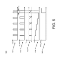
- FIG. 5 illustrates a timing diagram 500 of the signals of the resonant capacitor stabilizer 101 according to an implementation.
- the timing diagram 500 shows a signal waveform 501 generated by the timer 181 , the capacitor stabilization signal 502 sent to the second driver 154 that depicts the actuation duration of the second power switch 108 , the voltage (V ICS ) 503 of the integrated current sense signal, the voltage (V CR ) 504 of the resonant capacitor 110 , and the stabilization end signal 505 generated by on-time counter 186 .
- each pulse of the timer's signal waveform 501 starts a pulse of the capacitor stabilization signal 502 .
- the set terminal (S) of the latch 184 transitions to a logic high causing the output (Q) to transition to a logic high (thereby providing the capacitor stabilization signal 502 ), which instructs the second driver 154 to turn-on the second power switch 108 .
- a pulse width of the high state of the capacitor stabilization signal 502 indicates how long the second power driver 108 is activated to discharge the resonant capacitor 110 during a particular activation instance.
- the output of the comparator 182 is a logic high to reset the latch 184 to turn-off the second power switch 108 (thereby defining the end of the high state of a particular pulse of the capacitor stabilization signal 502 ).
- the voltage (V CR ) 504 of the resonant capacitor 110 is discharged (e.g., each activation causes the voltage (V CR ) 504 to decrease a certain amount until the resonant capacitor 110 is fully (or substantially) discharged.
- the on-time counter 186 transitions to a logic high (thereby providing the stabilization end signal), which disables the timer 181 .
- the high period of the capacitor stabilization signal 502 gradually becomes longer until reaching the threshold (T TH ) causing the end of the capacitor stabilization period in which the resonant capacitor 110 is fully discharged.
- FIG. 6 illustrates example simulation results 600 of the resonant capacitor stabilizer 101 according to an implementation.
- the simulation results 600 depict the various signals of FIG. 5 under a simulation scenario.
- the voltage (V CR ) of the resonant capacitor 110 is gradually discharged during the capacitor stabilization period.
- FIG. 7 illustrates example simulation results 700 of soft start operations with capacitor stabilization by the resonant capacitor stabilizer 101 according to an implementation.
- the soft start circuit 162 causes the oscillator 150 to generate alternating first and second clock signals. Over time, the soft start circuit 162 increases the duty cycle and decreases the frequency of the first and second clock signals. During the course of the soft start operations (as the duty cycle increases and the frequency decreases), the amount of current (I PRI ) on the primary side of the transformer 116 increases.
- FIG. 8 illustrates example simulation results 800 of soft start operations without using capacitor stabilization by the resonant capacitor stabilizer 101 according to an implementation.
- the amount of current (I PRI ) on the primary side of the transformer 116 increases.
- the operations of the resonant capacitor stabilizer 101 before the soft start operations reduces the amount of current spikes (I PRI ) on the primary side of the transformer 116 .
- the current (I PRI ) is gradually increased, thereby reducing the effects of having large current spikes in the second power switch 108 .
- a resonant converter for resonant capacitance stabilization during start-up includes an oscillator configured to generate a first clock signal to drive a first driver for a first power switch, and a second clock signal to drive a second driver for a second power switch during switching operations, and a resonant capacitor stabilizer configured to control the second driver to periodically activate the second power switch to discharge a resonant capacitor of a resonant network during initialization of the switching operations of the resonant converter.
- the resonant converter may include one or more of the following features (or any combination thereof).
- the resonant capacitor stabilizer may be configured to activate the second power switch for a first duration and activate the second power switch for a second duration such that the second power switch is deactivated during a period of time between the first duration and the second duration.
- the second duration may be longer than the first duration.
- the resonant capacitor stabilizer may be configured to deactivate the second power switch in response to a voltage of an integrated current sense signal being equal to or below a voltage threshold.
- the resonant converter may include an integrated current sense circuit connected to the resonant capacitor, and the integrated current sense circuit may be configured to sense the integrated current sense signal on a primary side of a transformer of the resonant network.
- the resonant capacitor stabilizer may be configured to receive the voltage of the integrated current sense signal, and compare the voltage of the integrated current sense signal to the voltage threshold.
- the resonant capacitor stabilizer may be configured to trigger a soft start circuit to start soft start operations in response to the second power switch being activated longer than a threshold.
- the resonant capacitor stabilizer may include a latch having a set terminal, a reset terminal, and an output terminal, where the output terminal of the latch may be connected to the second driver.
- the resonant capacitor stabilizer may include a timer connected to the set terminal of the latch, and a voltage comparator having a first input terminal connected to a voltage of an integrated current sense signal, a second input terminal connected to a reference voltage, and an output terminal connected to the reset terminal of the latch.
- the resonant capacitor stabilizer may include an on-time counter connected to the timer and the output terminal of the latch. The timer may be configured to periodically activate the set terminal of the latch such that the output terminal of the latch periodically sends a high state of a capacitor stabilization signal to the second driver to turn-on the second power switch to discharge the resonant capacitor.
- the on-time counter may be configured to count an activation time of the second power switch, and, in response to the activation time exceeding a threshold, the on-time counter is configured to send a stabilization end signal to the timer to end the discharging of the resonant capacitor.
- the voltage comparator may be configured to compare the voltage of the integrated current sense signal and the reference voltage, and, in response to the reference voltage being larger than the voltage of the integrated current sense signal, the voltage comparator is configured to reset the latch causing the second power switch to deactivate.
- a resonant converter for resonant capacitance stabilization during start-up includes an oscillator configured to generate a first clock signal to drive a first driver for a first power switch, and a second clock signal to drive a second driver for a second power switch during switching operations, and a resonant capacitor stabilizer configured to control the second driver to activate the second power switch to discharge a resonant capacitor of a resonant network during a capacitor stabilization period that occurs during initialization of the switching operations of the resonant converter.
- the resonant capacitor stabilizer is configured to control the second driver to deactivate the second power switch in response to a voltage of an integrated current sense signal being equal to or less than a threshold voltage.
- the resonant converter may include one of more of the above/below features (or any combination thereof).
- the resonant capacitor stabilizer may be configured to control the second driver to activate and deactivate multiple times during the capacitor stabilization period.
- the resonant capacitor stabilizer is configured to activate the second power switch at a first time and then deactivate the second power switch when the voltage of the integrated current sense signal is equal to or less than the threshold voltage such that the second power switch is activated for a first duration.
- the resonant capacitor stabilizer may be configured to activate the second power switch at a second time and then deactivate the second power switch when the voltage of the integrated current sense signal is equal to or less than the threshold voltage such that the second power switch is activated for a second duration.
- the second duration may be longer than the first duration.
- the resonant capacitor stabilizer may be configured to receive the integrated current sense signal sensed on a primary side of a transformer of the resonant network.
- the resonant converter may include an integrated current sense circuit connected to the resonant capacitor, where the integrated current sense circuit is configured to sense the integrated current sense signal on the primary side of the transformer of the resonant network, and the integrated current sense circuit includes a capacitor divider.
- the resonant capacitor stabilizer may be configured to trigger a soft start circuit to start soft start operations in response to an activation period of the second power switch being longer than a threshold.
- a resonant converter for resonant capacitance stabilization during start-up includes an oscillator configured to generate a first clock signal to drive a first driver for a first power switch, and a second clock signal to drive a second driver for a second power switch during switching operations, and a resonant capacitor stabilizer configured to control the second driver to activate the second power switch to discharge a resonant capacitor of a resonant network during initialization of the switching operations of the resonant converter.
- the resonant capacitor stabilizer includes a timer configured to periodically activate the second power switch, and an on-time counter is configured to count an activation time of the second power switch.
- the resonant capacitor stabilizer is configured to trigger a soft start circuit to start soft start operations in response to the activation time of the second power switch exceeding a threshold.
- the resonant converter may include one of more of the above/below features (or any combination thereof).
- the resonant capacitor stabilizer may be configured to deactivate the second power switch at each activation instance in response to a voltage of an integrated current sense signal being equal to or below a voltage threshold.
- the second power switch may be a low-side metal oxide semiconductor field effect transistor (MOSFET).
Landscapes
- Engineering & Computer Science (AREA)
- Power Engineering (AREA)
- Physics & Mathematics (AREA)
- General Physics & Mathematics (AREA)
- Dc-Dc Converters (AREA)
Abstract
Description
Claims (19)
Priority Applications (3)
| Application Number | Priority Date | Filing Date | Title |
|---|---|---|---|
| US15/668,975 US10193455B2 (en) | 2016-08-19 | 2017-08-04 | Resonant capacitor stabilizer in resonant converters |
| KR1020170104748A KR102226978B1 (en) | 2016-08-19 | 2017-08-18 | Resonant capacitor stabilizer in resonant converters |
| CN201721042467.8U CN207368881U (en) | 2016-08-19 | 2017-08-18 | For carrying out the resonance converter of resonant capacitance stabilization during startup |
Applications Claiming Priority (2)
| Application Number | Priority Date | Filing Date | Title |
|---|---|---|---|
| US201662377063P | 2016-08-19 | 2016-08-19 | |
| US15/668,975 US10193455B2 (en) | 2016-08-19 | 2017-08-04 | Resonant capacitor stabilizer in resonant converters |
Publications (2)
| Publication Number | Publication Date |
|---|---|
| US20180054133A1 US20180054133A1 (en) | 2018-02-22 |
| US10193455B2 true US10193455B2 (en) | 2019-01-29 |
Family
ID=61192297
Family Applications (4)
| Application Number | Title | Priority Date | Filing Date |
|---|---|---|---|
| US15/668,980 Active 2038-06-30 US10693379B2 (en) | 2016-08-19 | 2017-08-04 | Short-circuit protection using pulse width modulation (PWM) for resonant converters |
| US15/668,975 Active US10193455B2 (en) | 2016-08-19 | 2017-08-04 | Resonant capacitor stabilizer in resonant converters |
| US15/668,974 Active US10374516B2 (en) | 2016-08-19 | 2017-08-04 | Non zero-voltage switching (ZVS) detection in resonant converters |
| US15/668,983 Active US10186948B2 (en) | 2016-08-19 | 2017-08-04 | Burst mode control in resonant converters |
Family Applications Before (1)
| Application Number | Title | Priority Date | Filing Date |
|---|---|---|---|
| US15/668,980 Active 2038-06-30 US10693379B2 (en) | 2016-08-19 | 2017-08-04 | Short-circuit protection using pulse width modulation (PWM) for resonant converters |
Family Applications After (2)
| Application Number | Title | Priority Date | Filing Date |
|---|---|---|---|
| US15/668,974 Active US10374516B2 (en) | 2016-08-19 | 2017-08-04 | Non zero-voltage switching (ZVS) detection in resonant converters |
| US15/668,983 Active US10186948B2 (en) | 2016-08-19 | 2017-08-04 | Burst mode control in resonant converters |
Country Status (3)
| Country | Link |
|---|---|
| US (4) | US10693379B2 (en) |
| KR (4) | KR20180020920A (en) |
| CN (4) | CN107769567B (en) |
Cited By (1)
| Publication number | Priority date | Publication date | Assignee | Title |
|---|---|---|---|---|
| US20220286056A1 (en) * | 2021-03-03 | 2022-09-08 | Semiconductor Components Industries, Llc | Resonant converter with dual-mode control |
Families Citing this family (43)
| Publication number | Priority date | Publication date | Assignee | Title |
|---|---|---|---|---|
| US10693379B2 (en) | 2016-08-19 | 2020-06-23 | Semiconductor Components Industries, Llc | Short-circuit protection using pulse width modulation (PWM) for resonant converters |
| US10483855B2 (en) * | 2017-08-07 | 2019-11-19 | Semiconductor Components Industries, Llc | Power limit protection for resonant power converter |
| US10530617B2 (en) | 2017-08-07 | 2020-01-07 | Micron Technology, Inc. | Programmable channel equalization for multi-level signaling |
| US10277435B2 (en) * | 2017-08-07 | 2019-04-30 | Micron Technology, Inc. | Method to vertically align multi-level cells |
| US10447512B2 (en) | 2017-08-07 | 2019-10-15 | Micron Technology, Inc. | Channel equalization for multi-level signaling |
| WO2019183880A1 (en) * | 2018-03-29 | 2019-10-03 | 深圳驿普乐氏科技有限公司 | Llc resonant converter as well as control circuit and resonant current sampling circuit thereof |
| CN108923657B (en) * | 2018-07-02 | 2020-06-09 | 杭州茂力半导体技术有限公司 | Resonant converter and control circuit and control method thereof |
| US10838016B2 (en) * | 2018-07-06 | 2020-11-17 | Texas Instruments Incorporated | Short detect scheme for an output pin |
| KR102440976B1 (en) | 2018-07-27 | 2022-09-08 | 삼성디스플레이 주식회사 | Driving voltage provider |
| EP3624319A1 (en) * | 2018-09-14 | 2020-03-18 | Delta Electronics (Thailand) Public Co., Ltd. | Switch protection |
| DE102018124581B4 (en) * | 2018-10-05 | 2022-07-07 | Infineon Technologies Austria Ag | Power converter control, asymmetric power converter and method of operating a power converter |
| US10644591B1 (en) | 2018-10-16 | 2020-05-05 | Linear Technology Holding Llc | Regulator light load control techniques |
| US11081966B2 (en) * | 2018-12-13 | 2021-08-03 | Power Integrations, Inc. | Multi zone secondary burst modulation for resonant converters |
| US11196347B2 (en) * | 2018-12-13 | 2021-12-07 | Power Integrations, Inc. | Apparatus and methods for controlling a switch drive signal following mode transitions in a switching power converter |
| US11196351B2 (en) * | 2019-02-14 | 2021-12-07 | Texas Instruments Incorporated | Burst mode operation for a resonant converter |
| CN110212767B (en) * | 2019-04-30 | 2020-08-04 | 东南大学 | Digital control method for realizing multi-step frequency modulation of LL C resonant converter |
| TWI703423B (en) * | 2019-06-19 | 2020-09-01 | 群光電能科技股份有限公司 | Power supply device and a power supply method |
| CN110518679A (en) * | 2019-08-30 | 2019-11-29 | 南方电网科学研究院有限责任公司 | Controllable charging load circuit and control method thereof |
| CN110752750B (en) * | 2019-10-14 | 2021-09-10 | 成都芯源系统有限公司 | Resonant converter and control circuit and control method thereof |
| US10931204B1 (en) * | 2019-11-12 | 2021-02-23 | Monolithic Power Systems, Inc. | Isolated resonant converter with fixed output ripple |
| JP7493711B2 (en) * | 2019-11-22 | 2024-06-03 | 株式会社アパード | Power converter and control method thereof |
| KR102281633B1 (en) * | 2019-12-03 | 2021-07-23 | 엘에스일렉트릭(주) | Apparatus and method for controlling inverter |
| US11502597B2 (en) * | 2020-01-08 | 2022-11-15 | Infineon Technologies Austria Ag | Startup of a voltage converter |
| TWI728704B (en) * | 2020-02-17 | 2021-05-21 | 亞源科技股份有限公司 | Power factor correction circuit with burst setting and method for operation the same |
| CN112886820B (en) * | 2020-03-06 | 2022-11-18 | 陶顺祝 | Resonant circuit converter and control method |
| TWI725807B (en) * | 2020-04-07 | 2021-04-21 | 新唐科技股份有限公司 | Control system of voltage regulation and method thereof |
| JP7472654B2 (en) * | 2020-05-27 | 2024-04-23 | 富士電機株式会社 | Switching control circuit, LLC converter |
| CN111813000B (en) * | 2020-06-11 | 2023-04-11 | 广西电网有限责任公司电力科学研究院 | Method and device for simulating ferromagnetic resonance of power distribution network real-time test platform |
| CN113949272A (en) | 2020-06-30 | 2022-01-18 | 台达电子工业股份有限公司 | DC-DC resonant converter and control method thereof |
| CN112134453B (en) * | 2020-09-08 | 2021-10-29 | 台达电子企业管理(上海)有限公司 | Start control method and system, and peak voltage detection circuit and method |
| US11594948B2 (en) | 2021-02-09 | 2023-02-28 | Excelsys Tecnologies Ltd. | Reduced power consumption for LLC resonant converter under light load |
| JP2022142919A (en) * | 2021-03-17 | 2022-10-03 | 富士電機株式会社 | Switching control circuit and resonant converter |
| CN112821762B (en) * | 2021-04-16 | 2021-09-03 | 深圳市拓尔微电子有限责任公司 | Control circuit and booster circuit |
| CN216959654U (en) * | 2021-04-21 | 2022-07-12 | 友尚股份有限公司 | Power converter |
| CN113452254B (en) * | 2021-05-27 | 2023-03-31 | 华为数字能源技术有限公司 | Resonance transformation system and control method |
| CN115882703A (en) * | 2021-08-19 | 2023-03-31 | 力智电子股份有限公司 | Intelligent power level module, current monitoring signal generating circuit and method thereof |
| US11855544B2 (en) * | 2022-02-03 | 2023-12-26 | Lee Fredrik Mazurek | Single stage synchronous harmonic current controlled power system |
| US11755304B2 (en) * | 2022-02-04 | 2023-09-12 | Toshiba Tec Kabushiki Kaisha | Electric device and method for controlling same |
| WO2023231201A1 (en) | 2022-05-30 | 2023-12-07 | 上海新进芯微电子有限公司 | Control system for burst mode of switching power supply, and pwm controller |
| WO2024016301A1 (en) * | 2022-07-22 | 2024-01-25 | 华为数字能源技术有限公司 | Control circuit for asymmetrical half-bridge flyback circuit, power supply module, and electronic device |
| TWI837944B (en) * | 2022-11-15 | 2024-04-01 | 宏碁股份有限公司 | Power supply device with high output stability |
| US11855545B1 (en) * | 2023-09-10 | 2023-12-26 | Lee Fredrik Mazurek | Single stage synchronous generalized regulator |
| CN117175952B (en) * | 2023-11-01 | 2024-01-30 | 艾科微电子(深圳)有限公司 | Power supply controller, switch type power supply and control method |
Citations (17)
| Publication number | Priority date | Publication date | Assignee | Title |
|---|---|---|---|---|
| US5973943A (en) | 1998-01-05 | 1999-10-26 | International Rectifier Corporation | Non zero-voltage switching protection circuit |
| US6256210B1 (en) | 1999-05-26 | 2001-07-03 | U.S. Philips Corporation | Converter for conversion of an input voltage into an output voltage |
| US6331755B1 (en) | 1998-01-13 | 2001-12-18 | International Rectifier Corporation | Circuit for detecting near or below resonance operation of a fluorescent lamp driven by half-bridge circuit |
| US6496387B2 (en) | 2000-04-10 | 2002-12-17 | Koninklijke Phillips Electronics N.V. | Resonant converter comprising a control circuit |
| US6879115B2 (en) | 2002-07-09 | 2005-04-12 | International Rectifier Corporation | Adaptive ballast control IC |
| US7116561B2 (en) * | 2005-01-06 | 2006-10-03 | Sanken Electric Co., Ltd. | Resonant power source apparatus |
| US7323825B2 (en) | 2005-12-02 | 2008-01-29 | Fairchild Korea Semiconductor, Ltd. | Ballast integrated circuit (IC) |
| US20090244934A1 (en) | 2008-03-28 | 2009-10-01 | Delta Electronics Inc. | Synchronous rectification circuit having burst mode controller and controlling method thereof |
| US7750615B2 (en) | 2007-01-18 | 2010-07-06 | Fairchild Korea Semiconductor, Ltd. | Burst mode operation in a DC-DC converter |
| US20100202170A1 (en) | 2009-02-06 | 2010-08-12 | Jin-Tae Kim | Soft-Burst Circuit For Switched-Mode Power Supplies |
| US8014176B2 (en) | 2008-07-25 | 2011-09-06 | Cirrus Logic, Inc. | Resonant switching power converter with burst mode transition shaping |
| US20120307530A1 (en) | 2009-11-30 | 2012-12-06 | Panasonic Corporation | Power supply device and method for controlling same |
| US8737101B2 (en) | 2010-02-24 | 2014-05-27 | Fairchild Korea Semiconductor Ltd. | Switch driving circuit and switch driving method |
| US20150003117A1 (en) | 2013-06-26 | 2015-01-01 | Stmicroelectronics S.R.L. | Method of controlling a switching converter in burst mode and related controller for a switching converter |
| US20150229220A1 (en) * | 2014-02-11 | 2015-08-13 | Fairchild Korea Semiconductor Ltd. | Switch control circuit and resonant converter including the same |
| US9203318B2 (en) | 2013-12-18 | 2015-12-01 | Texas Instruments Deutschland Gmbh | Primary side current regulation on LLC converters for LED driving |
| US20180054134A1 (en) * | 2016-08-19 | 2018-02-22 | Fairchild Korea Semiconductor Ltd. | Burst mode control in resonant converters |
Family Cites Families (10)
| Publication number | Priority date | Publication date | Assignee | Title |
|---|---|---|---|---|
| CN102136801B (en) | 2010-01-21 | 2014-02-19 | 台达电子工业股份有限公司 | Resonant converter and intermittent mode control method thereof |
| EP2445098B1 (en) | 2010-10-25 | 2019-08-07 | STMicroelectronics Srl | Control device for a resonant converter. |
| CN102055310B (en) * | 2010-11-01 | 2013-09-11 | 崇贸科技股份有限公司 | Power supply unit with functions of open loop protection and short circuit protection |
| EP2458723B1 (en) | 2010-11-24 | 2016-08-17 | Nxp B.V. | A circuit for a resonant converter |
| US8730687B2 (en) | 2011-03-09 | 2014-05-20 | System General Corporation | Switching controller with valley-lock switching and limited maximum frequency for quasi-resonant power converters |
| US9143043B2 (en) | 2012-03-01 | 2015-09-22 | Infineon Technologies Ag | Multi-mode operation and control of a resonant converter |
| CN103457453B (en) | 2012-06-04 | 2016-05-11 | 台达电子工业股份有限公司 | A kind of control method for reducing audio noise |
| US20140009970A1 (en) | 2012-07-06 | 2014-01-09 | Power Systems Technologies, Ltd. | Controller for a Power Converter and Method of Operating the Same |
| CN104298331A (en) * | 2013-07-16 | 2015-01-21 | 鸿富锦精密工业(深圳)有限公司 | Power supply circuit for power supply control chip |
| US9257913B1 (en) * | 2014-09-06 | 2016-02-09 | Texas Instruments Incorporated | LLC converter and loss of inductive mode detection circuit |
-
2017
- 2017-08-04 US US15/668,980 patent/US10693379B2/en active Active
- 2017-08-04 US US15/668,975 patent/US10193455B2/en active Active
- 2017-08-04 US US15/668,974 patent/US10374516B2/en active Active
- 2017-08-04 US US15/668,983 patent/US10186948B2/en active Active
- 2017-08-18 CN CN201710709422.XA patent/CN107769567B/en active Active
- 2017-08-18 KR KR1020170104695A patent/KR20180020920A/en not_active Application Discontinuation
- 2017-08-18 CN CN201721037508.4U patent/CN207559860U/en active Active
- 2017-08-18 KR KR1020170104680A patent/KR20180020919A/en not_active Application Discontinuation
- 2017-08-18 CN CN201710709398.XA patent/CN107769583B/en active Active
- 2017-08-18 KR KR1020170104708A patent/KR102225011B1/en active IP Right Grant
- 2017-08-18 CN CN201721042467.8U patent/CN207368881U/en active Active
- 2017-08-18 KR KR1020170104748A patent/KR102226978B1/en active IP Right Grant
Patent Citations (17)
| Publication number | Priority date | Publication date | Assignee | Title |
|---|---|---|---|---|
| US5973943A (en) | 1998-01-05 | 1999-10-26 | International Rectifier Corporation | Non zero-voltage switching protection circuit |
| US6331755B1 (en) | 1998-01-13 | 2001-12-18 | International Rectifier Corporation | Circuit for detecting near or below resonance operation of a fluorescent lamp driven by half-bridge circuit |
| US6256210B1 (en) | 1999-05-26 | 2001-07-03 | U.S. Philips Corporation | Converter for conversion of an input voltage into an output voltage |
| US6496387B2 (en) | 2000-04-10 | 2002-12-17 | Koninklijke Phillips Electronics N.V. | Resonant converter comprising a control circuit |
| US6879115B2 (en) | 2002-07-09 | 2005-04-12 | International Rectifier Corporation | Adaptive ballast control IC |
| US7116561B2 (en) * | 2005-01-06 | 2006-10-03 | Sanken Electric Co., Ltd. | Resonant power source apparatus |
| US7323825B2 (en) | 2005-12-02 | 2008-01-29 | Fairchild Korea Semiconductor, Ltd. | Ballast integrated circuit (IC) |
| US7750615B2 (en) | 2007-01-18 | 2010-07-06 | Fairchild Korea Semiconductor, Ltd. | Burst mode operation in a DC-DC converter |
| US20090244934A1 (en) | 2008-03-28 | 2009-10-01 | Delta Electronics Inc. | Synchronous rectification circuit having burst mode controller and controlling method thereof |
| US8014176B2 (en) | 2008-07-25 | 2011-09-06 | Cirrus Logic, Inc. | Resonant switching power converter with burst mode transition shaping |
| US20100202170A1 (en) | 2009-02-06 | 2010-08-12 | Jin-Tae Kim | Soft-Burst Circuit For Switched-Mode Power Supplies |
| US20120307530A1 (en) | 2009-11-30 | 2012-12-06 | Panasonic Corporation | Power supply device and method for controlling same |
| US8737101B2 (en) | 2010-02-24 | 2014-05-27 | Fairchild Korea Semiconductor Ltd. | Switch driving circuit and switch driving method |
| US20150003117A1 (en) | 2013-06-26 | 2015-01-01 | Stmicroelectronics S.R.L. | Method of controlling a switching converter in burst mode and related controller for a switching converter |
| US9203318B2 (en) | 2013-12-18 | 2015-12-01 | Texas Instruments Deutschland Gmbh | Primary side current regulation on LLC converters for LED driving |
| US20150229220A1 (en) * | 2014-02-11 | 2015-08-13 | Fairchild Korea Semiconductor Ltd. | Switch control circuit and resonant converter including the same |
| US20180054134A1 (en) * | 2016-08-19 | 2018-02-22 | Fairchild Korea Semiconductor Ltd. | Burst mode control in resonant converters |
Non-Patent Citations (11)
Cited By (2)
| Publication number | Priority date | Publication date | Assignee | Title |
|---|---|---|---|---|
| US20220286056A1 (en) * | 2021-03-03 | 2022-09-08 | Semiconductor Components Industries, Llc | Resonant converter with dual-mode control |
| US11799382B2 (en) * | 2021-03-03 | 2023-10-24 | Semiconductor Components Industries, Llc | Resonant converter with dual-mode control |
Also Published As
| Publication number | Publication date |
|---|---|
| KR20180020922A (en) | 2018-02-28 |
| KR102225011B1 (en) | 2021-03-10 |
| KR102226978B1 (en) | 2021-03-15 |
| US10186948B2 (en) | 2019-01-22 |
| US20180054134A1 (en) | 2018-02-22 |
| US20180054111A1 (en) | 2018-02-22 |
| US20180054130A1 (en) | 2018-02-22 |
| CN207559860U (en) | 2018-06-29 |
| US10374516B2 (en) | 2019-08-06 |
| KR20180020921A (en) | 2018-02-28 |
| US10693379B2 (en) | 2020-06-23 |
| US20180054133A1 (en) | 2018-02-22 |
| CN207368881U (en) | 2018-05-15 |
| CN107769583B (en) | 2021-05-14 |
| KR20180020920A (en) | 2018-02-28 |
| CN107769567B (en) | 2020-12-11 |
| KR20180020919A (en) | 2018-02-28 |
| CN107769583A (en) | 2018-03-06 |
| CN107769567A (en) | 2018-03-06 |
Similar Documents
| Publication | Publication Date | Title |
|---|---|---|
| US10193455B2 (en) | Resonant capacitor stabilizer in resonant converters | |
| US11824453B2 (en) | Secondary controller for use in synchronous flyback converter | |
| US10186976B2 (en) | Peak switching and optimal SR drive timing control | |
| US10277130B2 (en) | Primary-side start-up method and circuit arrangement for a series-parallel resonant power converter | |
| US20180269797A1 (en) | Flyback converter with secondary side regulation | |
| JP5900607B2 (en) | Switching power supply | |
| CN106059304B (en) | Switch with efficient voltage reduction using secondary switches | |
| US20180076721A1 (en) | Quasi-resonant valley lockout without feedback reference | |
| US10693386B2 (en) | Current protected integrated transformer driver for isolating a DC-DC convertor | |
| US20150124495A1 (en) | Reducing power consumption of a synchronous rectifier controller | |
| US8625314B2 (en) | Switching power supply apparatus | |
| US20020131282A1 (en) | Switching power supply | |
| EP0736959B1 (en) | Low dissipation power controller | |
| EP2963793A1 (en) | A SMPC, controller therefor, power supply and a method of controlling a SMPC | |
| US12095377B2 (en) | Discharge prevention of the power switch in a power converter |
Legal Events
| Date | Code | Title | Description |
|---|---|---|---|
| AS | Assignment |
Owner name: FAIRCHILD KOREA SEMICONDUCTOR LTD., KOREA, REPUBLI Free format text: ASSIGNMENT OF ASSIGNORS INTEREST;ASSIGNORS:MOON, SANGCHEOL;KIM, JINTAE;CHOI, HANGSEOK;SIGNING DATES FROM 20170731 TO 20170803;REEL/FRAME:043200/0171 |
|
| AS | Assignment |
Owner name: SEMICONDUCTOR COMPONENTS INDUSTRIES, LLC, ARIZONA Free format text: ASSIGNMENT OF ASSIGNORS INTEREST;ASSIGNOR:FAIRCHILD KOREA SEMICONDUCTOR, LTD.;REEL/FRAME:044361/0205 Effective date: 20171102 |
|
| AS | Assignment |
Owner name: DEUTSCHE BANK AG NEW YORK BRANCH, AS COLLATERAL AGENT, NEW YORK Free format text: PATENT SECURITY AGREEMENT;ASSIGNORS:SEMICONDUCTOR COMPONENTS INDUSTRIES, LLC;FAIRCHILD SEMICONDUCTOR CORPORATION;REEL/FRAME:046530/0460 Effective date: 20171110 Owner name: DEUTSCHE BANK AG NEW YORK BRANCH, AS COLLATERAL AG Free format text: PATENT SECURITY AGREEMENT;ASSIGNORS:SEMICONDUCTOR COMPONENTS INDUSTRIES, LLC;FAIRCHILD SEMICONDUCTOR CORPORATION;REEL/FRAME:046530/0460 Effective date: 20171110 |
|
| STCF | Information on status: patent grant |
Free format text: PATENTED CASE |
|
| MAFP | Maintenance fee payment |
Free format text: PAYMENT OF MAINTENANCE FEE, 4TH YEAR, LARGE ENTITY (ORIGINAL EVENT CODE: M1551); ENTITY STATUS OF PATENT OWNER: LARGE ENTITY Year of fee payment: 4 |
|
| AS | Assignment |
Owner name: FAIRCHILD SEMICONDUCTOR CORPORATION, ARIZONA Free format text: RELEASE OF SECURITY INTEREST IN PATENTS RECORDED AT REEL 046530, FRAME 0460;ASSIGNOR:DEUTSCHE BANK AG NEW YORK BRANCH, AS COLLATERAL AGENT;REEL/FRAME:064075/0001 Effective date: 20230622 Owner name: SEMICONDUCTOR COMPONENTS INDUSTRIES, LLC, ARIZONA Free format text: RELEASE OF SECURITY INTEREST IN PATENTS RECORDED AT REEL 046530, FRAME 0460;ASSIGNOR:DEUTSCHE BANK AG NEW YORK BRANCH, AS COLLATERAL AGENT;REEL/FRAME:064075/0001 Effective date: 20230622 |