EP3964842A1 - Arrangement and switching device with contactless current measuring capability - Google Patents
Arrangement and switching device with contactless current measuring capability Download PDFInfo
- Publication number
- EP3964842A1 EP3964842A1 EP21193143.1A EP21193143A EP3964842A1 EP 3964842 A1 EP3964842 A1 EP 3964842A1 EP 21193143 A EP21193143 A EP 21193143A EP 3964842 A1 EP3964842 A1 EP 3964842A1
- Authority
- EP
- European Patent Office
- Prior art keywords
- electrical conductor
- resistance
- hall sensor
- housing
- switching device
- Prior art date
- Legal status (The legal status is an assumption and is not a legal conclusion. Google has not performed a legal analysis and makes no representation as to the accuracy of the status listed.)
- Granted
Links
Images



Classifications
-
- G—PHYSICS
- G01—MEASURING; TESTING
- G01R—MEASURING ELECTRIC VARIABLES; MEASURING MAGNETIC VARIABLES
- G01R15/00—Details of measuring arrangements of the types provided for in groups G01R17/00 - G01R29/00, G01R33/00 - G01R33/26 or G01R35/00
- G01R15/14—Adaptations providing voltage or current isolation, e.g. for high-voltage or high-current networks
- G01R15/20—Adaptations providing voltage or current isolation, e.g. for high-voltage or high-current networks using galvano-magnetic devices, e.g. Hall-effect devices, i.e. measuring a magnetic field via the interaction between a current and a magnetic field, e.g. magneto resistive or Hall effect devices
- G01R15/202—Adaptations providing voltage or current isolation, e.g. for high-voltage or high-current networks using galvano-magnetic devices, e.g. Hall-effect devices, i.e. measuring a magnetic field via the interaction between a current and a magnetic field, e.g. magneto resistive or Hall effect devices using Hall-effect devices
-
- G—PHYSICS
- G01—MEASURING; TESTING
- G01R—MEASURING ELECTRIC VARIABLES; MEASURING MAGNETIC VARIABLES
- G01R19/00—Arrangements for measuring currents or voltages or for indicating presence or sign thereof
- G01R19/0092—Measuring current only
-
- G—PHYSICS
- G01—MEASURING; TESTING
- G01R—MEASURING ELECTRIC VARIABLES; MEASURING MAGNETIC VARIABLES
- G01R1/00—Details of instruments or arrangements of the types included in groups G01R5/00 - G01R13/00 and G01R31/00
- G01R1/20—Modifications of basic electric elements for use in electric measuring instruments; Structural combinations of such elements with such instruments
- G01R1/203—Resistors used for electric measuring, e.g. decade resistors standards, resistors for comparators, series resistors, shunts
-
- G—PHYSICS
- G01—MEASURING; TESTING
- G01R—MEASURING ELECTRIC VARIABLES; MEASURING MAGNETIC VARIABLES
- G01R1/00—Details of instruments or arrangements of the types included in groups G01R5/00 - G01R13/00 and G01R31/00
- G01R1/30—Structural combination of electric measuring instruments with basic electronic circuits, e.g. with amplifier
-
- G—PHYSICS
- G01—MEASURING; TESTING
- G01R—MEASURING ELECTRIC VARIABLES; MEASURING MAGNETIC VARIABLES
- G01R15/00—Details of measuring arrangements of the types provided for in groups G01R17/00 - G01R29/00, G01R33/00 - G01R33/26 or G01R35/00
- G01R15/14—Adaptations providing voltage or current isolation, e.g. for high-voltage or high-current networks
- G01R15/146—Measuring arrangements for current not covered by other subgroups of G01R15/14, e.g. using current dividers, shunts, or measuring a voltage drop
-
- G—PHYSICS
- G01—MEASURING; TESTING
- G01R—MEASURING ELECTRIC VARIABLES; MEASURING MAGNETIC VARIABLES
- G01R15/00—Details of measuring arrangements of the types provided for in groups G01R17/00 - G01R29/00, G01R33/00 - G01R33/26 or G01R35/00
- G01R15/14—Adaptations providing voltage or current isolation, e.g. for high-voltage or high-current networks
- G01R15/20—Adaptations providing voltage or current isolation, e.g. for high-voltage or high-current networks using galvano-magnetic devices, e.g. Hall-effect devices, i.e. measuring a magnetic field via the interaction between a current and a magnetic field, e.g. magneto resistive or Hall effect devices
- G01R15/207—Constructional details independent of the type of device used
-
- H—ELECTRICITY
- H01—ELECTRIC ELEMENTS
- H01H—ELECTRIC SWITCHES; RELAYS; SELECTORS; EMERGENCY PROTECTIVE DEVICES
- H01H71/00—Details of the protective switches or relays covered by groups H01H73/00 - H01H83/00
- H01H71/04—Means for indicating condition of the switching device
-
- H—ELECTRICITY
- H01—ELECTRIC ELEMENTS
- H01H—ELECTRIC SWITCHES; RELAYS; SELECTORS; EMERGENCY PROTECTIVE DEVICES
- H01H9/00—Details of switching devices, not covered by groups H01H1/00 - H01H7/00
- H01H9/02—Bases, casings, or covers
-
- H—ELECTRICITY
- H01—ELECTRIC ELEMENTS
- H01H—ELECTRIC SWITCHES; RELAYS; SELECTORS; EMERGENCY PROTECTIVE DEVICES
- H01H71/00—Details of the protective switches or relays covered by groups H01H73/00 - H01H83/00
- H01H71/04—Means for indicating condition of the switching device
- H01H2071/048—Means for indicating condition of the switching device containing non-mechanical switch position sensor, e.g. HALL sensor
Definitions
- the invention relates to an arrangement, comprising a first electrical conductor having a first resistance and a second electrical conductor, which is switched in parallel with the first electrical conductor and which has a second, higher resistance. Both the first resistance and the second resistance each are below 0.1 ⁇ between connection points between the first electrical conductor and the second electrical conductor. Furthermore, the invention relates to a switching device, which comprises a housing, two main terminals reaching through the housing and a conductive main current path, which connects the two main terminals within the housing.
- the main current path comprises a first electrical conductor having a first resistance
- the switching device comprises a switch arranged in the main current path.
- one problem of the invention is to provide an improved arrangement and to provide an improved switching device with contactless current measuring capability.
- a possibility for contactless measurement of high currents shall be provided.
- the object of the invention is also solved by a switching device as disclosed in the opening paragraph, additionally comprising
- the switching device can be embodied as a circuit breaker, which is a switching device with trigger unit automatically triggering the switch in a fault condition, e.g. in case of overcurrent or in case of a fault current.
- the switching device may also comprise a calculation unit, which is connected to the hall sensor and which is designed to calculate a total current through the first electrical conductor and the second electrical conductor based on the current measured by the hall sensor and based on a ratio between the first resistance and the second resistance or based on a ratio between the total resistance, which is the sum of the first resistance and the second resistance, and the second resistance.
- a calculation unit which is connected to the hall sensor and which is designed to calculate a total current through the first electrical conductor and the second electrical conductor based on the current measured by the hall sensor and based on a ratio between the first resistance and the second resistance or based on a ratio between the total resistance, which is the sum of the first resistance and the second resistance, and the second resistance.
- the switching device can be seen as comprising an arrangement of the aforementioned kind, which is arranged in the main current path within the housing.
- the calculation unit may also be an external calculation unit, which is arranged out of the housing and even at a distance from the switching device.
- a current I 1 flows trough first electrical conductor, and a current I 2 flows through the second electrical conductor, wherein a total current I T is the sum of both.
- the result i.e. the value of the total current I T can be communicated to a receiving party via a wired or wireless data interface, which is connected to the calculation unit and which can also be part of the above arrangement or the above switching device.
- the calculation unit and the data interface together can form an processing unit.
- the sum of the first resistance R 1 and the second resistance R 2 in the given context may also denoted as "parallel sum”.
- the current through the second electrical conductor can be kept small so that the magnetic field and hence the signal to be measured by the hall sensor are also comparably small.
- the limited measuring range of a hall sensor can be expanded, and comparably small hall sensors can be used for measuring high currents.
- the hall sensor can be arranged
- Near to in the above context in particular means that at least 95% of the magnetic field, which the hall sensor measures, originates from the second electrical conductor.
- a magnetic flux caused by the current through the second electrical conductor is concentrated within the magnetic core.
- an influence on the hall sensor caused by interfering magnetic fields can be kept low so that the measurement is not deteriorated by those interfering magnetic fields.
- an influence from an interfering magnetic field caused by the current through the first electrical conductor is thereby kept low.
- the magnetic flux in the annular magnetic core and thus the signal measured by the hall sensor can be increased compared to embodiments without such windings. Accordingly, provided the same sensitivity of the hall sensor, the current through the second electrical conductor can be lowered by the use of windings compared to embodiments without such windings.
- the air gap of the annular magnetic core can be filled out by the hall sensor, or there may also be an additional "true” air gap.
- an insulation between the second electrical conductor and conducting structures of the hall sensor (and also to the connection to the calculating unit and to conducting structures of the calculation unit) is designed to operate at least until a voltage of 1 kV or withstand at least a voltage of 1 kV. In this way, the risk for a flashover from the second electrical conductor to the calculation unit, the data interface and electronic circuits connected thereto is very low.
- the first electrical conductor and the second electrical conductor are embodied as a single piece.
- the first electrical conductor and the second electrical conductor can be made of a one-piece metal bar. So, the first electrical conductor and the second electrical conductor are easy to produce, for example by punching or laser cutting the desired shape out of a metal sheet material. But it is also beneficial if the second electrical conductor is made of or comprises a wire, in particular a stranded wire. In this way, the arrangement provides enhanced flexibility with regards to where the hall sensor can be arranged in relation to the first electrical conductor.
- the first and the second electrical conductor can be made from copper, steel, aluminum, brass or another metal alloy.
- a magnetic shielding is arranged around the hall sensor.
- a magnetic field interfering with the magnetic field originating from the current through the second electrical conductor is kept away from the hall sensor so that the measurement is not deteriorated by those interfering magnetic fields.
- an interfering magnetic field caused by the current through the first electrical conductor is thereby kept away from the hall sensor.
- a magnetic shielding shall not derogate a magnetic field in the magnetic cores of the cases b) to d) mentioned hereinbefore which originates from the current through the second electrical conductor.
- a quotient Q between the second resistance R 2 and the first resistance R 1 is greater than 2.
- Q R 2 /R 1 > 2 and R 1 ⁇ 0.5 ⁇ R 2 .
- this choice reduces the operational requirements of the hall sensor meaning that its measuring range can be comparably low and it can be smaller.
- this choice diminishes power consumption of R 2 and heating up the same.
- the quotient Q can also be greater than 5 or even greater than 10.
- the hall sensor is arranged within the housing.
- the switching device and the hall sensor form an integrated solution.
- the calculation unit and also the data interface can be arranged within the housing.
- the calculation unit and/or the data interface can also be arranged out of the housing.
- the hall sensor and also the calculation unit and also the data interface can be detachably connected to the housing.
- switching devices can be retrofitted with a current sensing device, comprising the hall sensor, the calculation unit and the data interface if desired.
- the second electrical conductor is lead through the housing and the hall sensor is arranged out of the housing.
- the second electrical conductor can comprise a first part and a second part, wherein the first part of the second electrical conductor can be detachably connected to secondary terminals of the switching device, which are electrically connected to the second parts of the second electrical conductor within the housing.
- the hall sensor and also the calculation unit and also the data interface can be detachably connected to the housing. That also means that the calculation unit and also the data interface can be arranged out of the housing, too.
- this embodiment provides retrofitting switching devices with a current sensing device, comprising the hall sensor, the calculation unit and the data interface if desired.
- the hall sensor or the current sensing device can be embodied as plug-in device or plug-on device.
- the second electrical conductor is lead to the housing and runs near to or within the housing in a contactless region and the hall sensor is arranged out of the housing in this contactless region.
- the second electrical conductor runs in parallel to an outer border of the housing in the contactless region.
- This embodiment takes advantage of the contactless measuring capability of the hall sensor.
- the second electrical conductor needs not to be lead through the housing and there is no need for secondary terminals, which generally involve the risk of electrical shocks if they are not covered properly when no current sensing device is attached to the switching device.
- the embodiment in question does not need such a cover and hence is particularly safe.
- the calculation unit and the data interface can be arranged out of the housing, too.
- the hall sensor and also the calculation unit and also the data interface can be detachably connected to the housing. In that, switching devices again can be retrofitted with a current sensing device, comprising the hall sensor, the calculation unit and the data interface if desired.
- Fig. 1 shows a first example of an arrangement 1a for measuring a current.
- the arrangement 1a comprises a metal bar 2, which has common electrical conductors 3a, 3b, a first electrical conductor 4 and a second electrical conductor 5.
- the first electrical conductor 4 is switched in parallel with the second electrical conductor 5, and both are connected to each other at connection points P 1 , P 2 .
- the metal bar 2 is one-piece and the common electrical conductors 3a, 3b, the first electrical conductor 4 and a second electrical conductor 5 are sections thereof.
- the first electrical conductor 4 has a first resistance R 1
- the second electrical conductor 5 has a second, higher resistance R 2 , wherein the first resistance R 1 and the second resistance R 2 each are below 0.1 ⁇ between connection points P 1 , P 2 between the first electrical conductor 4 and the second electrical conductor 5.
- the metal bar 2 comprises optional mounting holes 6a, 6b, by which the arrangement 1a can be switched into an electric circuit.
- the arrangement 1a furthermore comprises a hall sensor 8, which is mounted to the second electrical conductor 5 with an insulation 7 in-between. Further on, the arrangement 1a comprises a calculation unit 9, which is connected to the hall sensor 8 at an input side and which is connected to a wireless data interface 10 on its output side. The calculation unit 9 and the wireless data interface 10 together form a processing unit 11.
- the hall sensor 8 measures the current I 2 through the second electrical conductor 5, and the calculation unit 9 calculates the total current I T through the first electrical conductor 4 and the second electrical conductor 5 based on the current I 2 measured by the hall sensor 8 and based on a ratio between the first resistance R 1 and the second resistance R 2 or based on a ratio between the total resistance, which is the sum of the first resistance R 1 and the second resistance R 2 , and the second resistance R 2 .
- the result i.e. the value of the total current I T can be communicated to a receiving party via the wireless data interface 10.
- a wired data interface would be applicable as well.
- a quotient Q between the second resistance R 2 and the first resistance R 1 is greater than 2.
- Q R 2 /R 1 > 2 and R 1 ⁇ 0.5 ⁇ R 2 .
- this choice reduces the operational requirements of the hall sensor 8 meaning that its measuring range can be comparably low and it can be smaller.
- this choice diminishes power consumption of R 2 and heating up the same.
- the quotient Q can also be greater than 5 or even greater than 10.
- An advantage of using the arrangement 1a for measuring the total current I T is that comparably large currents can be measured with high accuracy and with having galvanic separation.
- the insulation 7 between the second electrical conductor 5 and conducting structures of the hall sensor 8 is designed to operate until or withstand at least a voltage of 1 kV.
- Fig. 2 shows a second embodiment of an arrangement 1b for measuring a current, which is similar to the arrangement 1a shown in Fig. 1 .
- a magnetic shielding 12 is arranged around the hall sensor 8.
- a magnetic field interfering with the magnetic field originating from the current I 2 through the second electrical conductor 5 is kept away from the hall sensor 8 so that the measurement is not deteriorated by those interfering magnetic fields.
- an interfering magnetic field caused by the current I 1 through the first electrical conductor 4 is thereby kept away from the hall sensor 8.
- Fig. 3 shows another embodiment of an arrangement 1c for measuring a current, which is similar to the arrangement 1a shown in Fig. 1 .
- an annular magnetic core 13a surrounds the second electrical conductor 5, and the hall sensor 8 is located in an air gap G of this annular magnetic core 13a.
- Fig. 4 shows a side view of the arrangement 1c of Fig. 3 in the plane AA.
- a magnetic flux caused by the current I 2 through the second electrical conductor 5 is concentrated within the annular magnetic core 13a.
- an influence on the hall sensor 8 caused by interfering magnetic fields can be kept low so that the measurement is not deteriorated by those interfering magnetic fields as well.
- Fig. 5 shows another embodiment of an arrangement 1d for measuring a current, which is similar to the arrangement 1a shown in Fig. 1 .
- the second electrical conductor 5 is made of or comprises a wire, in particular a stranded wire. So, the arrangement 1d provides enhanced flexibility with regards to where the hall sensor 8 can be arranged in relation to the first electrical conductor 4.
- the wire can be welded or soldered to the metal bar 2.
- Fig. 6 shows another embodiment of an arrangement 1e for measuring a current, which is similar to the arrangement 1c shown in Figs. 3 and 4 .
- the second electrical conductor 5 is wound around an annular magnetic core 13a, wherein the hall sensor 8 again is located in an air gap G of this annular magnetic core 13a.
- an air gap G of the annular magnetic core 13a can be filled out by the hall sensor 8 like this is depicted in Fig. 5 , or there may also be an additional "true” air gap like this is depicted in Figs. 3 and 4 .
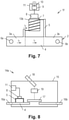
- Fig. 7 shows another embodiment of an arrangement 1f for measuring a current, which is similar to the arrangement 1e shown in Fig. 5 .
- the second electrical conductor 5 is not wound around an annular magnetic core 13a, but around an open, non-annular magnetic core 13b.
- the hall sensor 8 is arranged on the non-annular magnetic core 13b like this is depicted in Fig. 6 or near to the non-annular magnetic core 13b.
- a magnetic flux caused by the current I 2 through the second electrical conductor 5 is guided in the magnetic core 13b. That is why an influence of interfering magnetic fields again can be kept low so that the measurement is not deteriorated by those interfering magnetic fields.
- a magnetic core 13a, 13b in addition to the advantages noted above, helps to increase the distance of the hall sensor 8 from the first electrical conductor 4 what reduces an influence of the current I 1 trough first electrical conductor 4 on the measurement of the hall sensor 8, too, and also enhances design freedom.
- the hall sensor 8 can be arranged:
- Near to in the above context in particular means that at least 95% of the magnetic field, which the hall sensor 8 measures, originates from the current I 2 through the second electrical conductor 5.
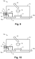
- Fig. 8 shows a first embodiment of a switching device 14a, which comprises a housing 15, two main terminals 16a, 16b reaching through the housing 15 and a (conductive) main current path, which connects the two main terminals 16a, 16b within the housing 15. Furthermore, the switching device 14a comprises a switch 17 arranged in the main current path. A lever 18 and a trigger unit 19 are connected to the switch 17 to operate the same manually and automatically in an overcurrent situation as is generally known.
- the main current path comprises a first electrical conductor 4 having a first resistance R 1 .
- a second electrical conductor 5 is switched in parallel to the first electrical conductor 4 and has a second, higher resistance R 2 .
- the switching device 14a also comprises a hall sensor 8, which is prepared to measure a current I 2 through the second electrical conductor 5.
- the first resistance R 1 and the second resistance R 2 are each are below 0.1 ⁇ between connection points P 1 , P 2 between the first electrical conductor 4 and the second electrical conductor 5.
- the switching device 14a can comprise a calculation unit 9 which is connected to the hall sensor 8 and which is designed to calculate a total current I T through the first electrical conductor 4 and the second electrical conductor 5 based on the current I 2 measured by the hall sensor 8 and based on a ratio between the first resistance R 1 and the second resistance R 2 or based on a ratio between the total resistance, which is the sum of the first resistance R 1 and the second resistance R 2 , and the second resistance R 2 .
- a calculation unit 9 which is connected to the hall sensor 8 and which is designed to calculate a total current I T through the first electrical conductor 4 and the second electrical conductor 5 based on the current I 2 measured by the hall sensor 8 and based on a ratio between the first resistance R 1 and the second resistance R 2 or based on a ratio between the total resistance, which is the sum of the first resistance R 1 and the second resistance R 2 , and the second resistance R 2 .
- the hall sensor 8 is arranged within the housing 15.
- the calculation unit 9 and also the data interface 10 is arranged within the housing 15 in Fig. 8 .
- Such a switching device 14a then can be seen as comprising an arrangement 1a..1f according to the examples disclosed hereinbefore, which is arranged in the main current path within the housing 15.
- the hall sensor 8 of the switching device 14a can also be connected to an external calculation unit 9 and communicate with the same by wire or wirelessly.
- the hall sensor 8, the calculation unit 9 and the data interface 10 can be arranged out of the housing 15.
- the hall sensor 8 and also the calculation unit 9 and also the data interface 10 can be detachably connected to the housing 15.
- Fig. 9 shows another embodiment of a switching device 14b, which is similar to the switching device 14a shown in Fig. 8 .
- the second electrical conductor comprises a first part 5a and a second part 5b.
- the first part 5a of the second electrical conductor is detachably connected to secondary terminals 20, which are electrically connected to the second parts 5b of the second electrical conductor within the housing 15.
- the hall sensor 8 is arranged out of the housing 15.
- the calculation unit 9 and also the data interface 10 are arranged out of the housing 15, too. So, the second electrical conductor 5a, 5b is lead through the housing 15 in this example.
- the hall sensor 8 and also the calculation unit 9 and also the data interface 10 can be detachably connected to the housing 15 as this is depicted in Fig. 9 .
- switching devices 14b can be retrofitted with a current sensing device, comprising the hall sensor 8, the calculation unit 9 and the data interface 10, if desired.
- Fig. 10 shows another embodiment of a switching device 14c, which is similar to the switching device 14b shown in Fig. 9 .
- the second electrical conductor 5 is lead to the housing 15 and runs near to or within the housing 15 in a contactless region C, and the hall sensor 8 is arranged out of the housing 15 in this contactless region C.
- the second electrical conductor 5 runs in parallel to an outer border of the housing 15 in the contactless region C like this is depicted in Fig. 10 .
- the hall sensor 8, the calculation unit 9 and also the data interface 10 are arranged out of the housing 15, and again it is advantageous if the hall sensor 8, the calculation unit 9 and also the data interface 10 are detachably connected to the housing 15.
- switching devices 14c can be retrofitted with a current sensing device, comprising the hall sensor 8, the calculation unit 9 and the data interface 10, if desired, too.
- the embodiment shown in Fig. 10 takes advantage of the contactless measuring capability of the hall sensor 8.
- the second electrical conductor 5 needs not to be lead through the housing 15 and there is no need for secondary terminals 20, which generally involve the risk of electrical shocks if they are not covered properly when no current sensing device is attached to the switching device 14b.
- the embodiment of Fig. 10 does not need such a cover and hence is particularly safe.
- Fig. 11 shows another embodiment of a switching device 14d, which is similar to the switching device 14c shown in Fig. 10 .
- an annular magnetic core 13a around the second electrical conductor 5 is used to guide the magnetic flux, which is caused by a current I 2 in the second electrical conductor 5, to the hall sensor 8.
- the hall sensor 8 is arranged in a gap G in the annular magnetic core 13a, just like it is the case in the example shown in Figs. 3 and 4 . So, the working principle and the advantages resulting thereof disclosed for the arrangement 1c of Figs. 3 and 4 are applicable to the switching device 14d of Fig. 11 equivalently.
- the housing 15 can fully enclose the annular magnetic core 13a, meaning that the hall sensor 8 is positioned in a groove of the housing 15 which is located in the air gap G of the annular magnetic core 13a.
- this embodiment is another example which is particularly useful for retrofitting a switching device 14d with a current sensing device, comprising the hall sensor 8, the calculation unit 9 and the data interface 10, if desired.
- the switching device 14d shown in Fig. 11 takes advantage of the contactless measuring capability of the hall sensor 8, and again there is no need to lead the second electrical conductor 5 through the housing 15 and no need for secondary terminals 20.
- the switching device 14d is particularly safe as well.
- Fig. 12 shows another embodiment of a switching device 14e, which is similar to the switching device 14d shown in Fig. 11 .
- an open, non-annular magnetic core 13b is used, around which the second electrical conductor 5 is wound. So, again the magnetic flux, which is caused by a current I 2 in the second electrical conductor 5, is guided to the hall sensor 8.
- the working principle and the advantages resulting thereof disclosed for the arrangement 1f shown in Fig. 7 are applicable to the switching device 14e of Fig. 12 equivalently.
- the housing 15 can fully enclose the annular magnetic core 13b, meaning that the hall sensor 8 is positioned out of the housing 15.
- this embodiment is another example which is particularly useful for retrofitting a switching device 14e with a current sensing device, comprising the hall sensor 8, the calculation unit 9 and the data interface 10, if desired.
- the switching device 14e shown in Fig. 12 takes advantage of the contactless measuring capability of the hall sensor 8, and again there is no need to lead the second electrical conductor 5 through the housing 15 and no need for secondary terminals 20.
- the switching device 14e is particularly safe as well.
- the hall sensor 8 in a switching device 14a..14e can be arranged:
- the invention is not limited to the embodiments disclosed hereinbefore, but combinations of the different variants are possible.
- the arrangements 1a..1f and the switching devices 14a..14e may have more or less parts than shown in the figures.
- the arrangements 1a..1f and the switching devices 14a..14e as well as parts thereof may also be shown in different scales and may be bigger or smaller than depicted.
- the description may comprise subject matter of further independent inventions.
Landscapes
- Physics & Mathematics (AREA)
- General Physics & Mathematics (AREA)
- Measuring Instrument Details And Bridges, And Automatic Balancing Devices (AREA)
Abstract
Description
- The invention relates to an arrangement, comprising a first electrical conductor having a first resistance and a second electrical conductor, which is switched in parallel with the first electrical conductor and which has a second, higher resistance. Both the first resistance and the second resistance each are below 0.1 Ω between connection points between the first electrical conductor and the second electrical conductor. Furthermore, the invention relates to a switching device, which comprises a housing, two main terminals reaching through the housing and a conductive main current path, which connects the two main terminals within the housing. The main current path comprises a first electrical conductor having a first resistance, and the switching device comprises a switch arranged in the main current path.
- Generally, such an arrangement and such a switching device are known. There are also known various methods and arrangements for current measuring. However, there is missing a possibility for contactless measurement of high currents.
- Accordingly, one problem of the invention is to provide an improved arrangement and to provide an improved switching device with contactless current measuring capability. In particular, a possibility for contactless measurement of high currents shall be provided.
- The object of the invention is solved by an arrangement as disclosed in the opening paragraph, additionally comprising
- a hall sensor, which is prepared to measure a current through the second electrical conductor, and
- a calculation unit, which is connected to the hall sensor and which is designed to calculate a total current through the first electrical conductor and the second electrical conductor based on the current measured by the hall sensor and based on a ratio between the first resistance and the second resistance or based on a ratio between the total resistance, which is the sum of the first resistance and the second resistance, and the second resistance.
- The object of the invention is also solved by a switching device as disclosed in the opening paragraph, additionally comprising
- a second electrical conductor, which is switched in parallel to the first electrical conductor and which has a second, higher resistance, and
- a hall sensor, which is prepared to measure a current through the second electrical conductor,
- wherein the first resistance and the second resistance each are below 0.1 Ω between connection points between the first electrical conductor and the second electrical conductor.
- Beneficially, the switching device can be embodied as a circuit breaker, which is a switching device with trigger unit automatically triggering the switch in a fault condition, e.g. in case of overcurrent or in case of a fault current.
- In particular, the switching device may also comprise a calculation unit, which is connected to the hall sensor and which is designed to calculate a total current through the first electrical conductor and the second electrical conductor based on the current measured by the hall sensor and based on a ratio between the first resistance and the second resistance or based on a ratio between the total resistance, which is the sum of the first resistance and the second resistance, and the second resistance.
- In this case, the switching device can be seen as comprising an arrangement of the aforementioned kind, which is arranged in the main current path within the housing. However, the calculation unit may also be an external calculation unit, which is arranged out of the housing and even at a distance from the switching device.
- When a voltage is applied between connection points between the first electrical conductor and the second electrical conductor, a current I1 flows trough first electrical conductor, and a current I2 flows through the second electrical conductor, wherein a total current IT is the sum of both. As generally known the relation between the currents is IT = I1+I2 and I1 · R1 = I2 · R2 in the arrangement defined above. The total current IT can be calculated by calculating the current I1 = I2 · R2/R1 and by subsequently calculating IT = I1+I2 or by directly calculating IT = I2 · (R1+R2)/R1 or by IT = I2 · (1+R2/R1).
- The result, i.e. the value of the total current IT can be communicated to a receiving party via a wired or wireless data interface, which is connected to the calculation unit and which can also be part of the above arrangement or the above switching device. The calculation unit and the data interface together can form an processing unit.
- The sum of the first resistance R1 and the second resistance R2 in the given context may also denoted as "parallel sum".
- By these measures, a device for contactless measurement of high currents is provided. Advantageously, the current through the second electrical conductor can be kept small so that the magnetic field and hence the signal to be measured by the hall sensor are also comparably small. In this way, the limited measuring range of a hall sensor can be expanded, and comparably small hall sensors can be used for measuring high currents.
- Generally, the hall sensor can be arranged
- a) on or near to the second electrical conductor or
- b) in an air gap of an annular magnetic core around the second electrical conductor or
- c) in an air gap of an annular magnetic core around which the second electrical conductor is wound or
- d) on or near an open, non-annular magnetic core around which the second electrical conductor is wound.
- "Near to" in the above context in particular means that at least 95% of the magnetic field, which the hall sensor measures, originates from the second electrical conductor.
- By using a magnetic core, a magnetic flux caused by the current through the second electrical conductor is concentrated within the magnetic core. Hence, an influence on the hall sensor caused by interfering magnetic fields can be kept low so that the measurement is not deteriorated by those interfering magnetic fields. In particular, an influence from an interfering magnetic field caused by the current through the first electrical conductor is thereby kept low.
- By winding the second electrical conductor around the magnetic core, the magnetic flux in the annular magnetic core and thus the signal measured by the hall sensor can be increased compared to embodiments without such windings. Accordingly, provided the same sensitivity of the hall sensor, the current through the second electrical conductor can be lowered by the use of windings compared to embodiments without such windings.
- The air gap of the annular magnetic core can be filled out by the hall sensor, or there may also be an additional "true" air gap.
- Further advantageous embodiments are disclosed in the claims and in the description as well as in the figures.
- Preferably, an insulation between the second electrical conductor and conducting structures of the hall sensor (and also to the connection to the calculating unit and to conducting structures of the calculation unit) is designed to operate at least until a voltage of 1 kV or withstand at least a voltage of 1 kV. In this way, the risk for a flashover from the second electrical conductor to the calculation unit, the data interface and electronic circuits connected thereto is very low.
- In another preferred embodiment, the first electrical conductor and the second electrical conductor are embodied as a single piece. In particular, the first electrical conductor and the second electrical conductor can be made of a one-piece metal bar. So, the first electrical conductor and the second electrical conductor are easy to produce, for example by punching or laser cutting the desired shape out of a metal sheet material. But it is also beneficial if the second electrical conductor is made of or comprises a wire, in particular a stranded wire. In this way, the arrangement provides enhanced flexibility with regards to where the hall sensor can be arranged in relation to the first electrical conductor. Generally, the first and the second electrical conductor can be made from copper, steel, aluminum, brass or another metal alloy.
- Advantageously, a magnetic shielding is arranged around the hall sensor. Hence, a magnetic field interfering with the magnetic field originating from the current through the second electrical conductor is kept away from the hall sensor so that the measurement is not deteriorated by those interfering magnetic fields. In particular, an interfering magnetic field caused by the current through the first electrical conductor is thereby kept away from the hall sensor. Of course, a magnetic shielding shall not derogate a magnetic field in the magnetic cores of the cases b) to d) mentioned hereinbefore which originates from the current through the second electrical conductor.
- Preferably, a quotient Q between the second resistance R2 and the first resistance R1 is greater than 2. In other words that means Q = R2/R1 > 2 and R1 < 0.5 · R2. Firstly, this choice reduces the operational requirements of the hall sensor meaning that its measuring range can be comparably low and it can be smaller. Secondly, this choice diminishes power consumption of R2 and heating up the same. To even increase these benefits, the quotient Q can also be greater than 5 or even greater than 10.
- In an advantageous embodiment of the switching device, the hall sensor is arranged within the housing. Hence, the switching device and the hall sensor form an integrated solution. In addition, the calculation unit and also the data interface can be arranged within the housing. However, the calculation unit and/or the data interface can also be arranged out of the housing. Moreover, the hall sensor and also the calculation unit and also the data interface can be detachably connected to the housing. In that, switching devices can be retrofitted with a current sensing device, comprising the hall sensor, the calculation unit and the data interface if desired.
- In another advantageous embodiment of the switching device, the second electrical conductor is lead through the housing and the hall sensor is arranged out of the housing. In particular, the second electrical conductor can comprise a first part and a second part, wherein the first part of the second electrical conductor can be detachably connected to secondary terminals of the switching device, which are electrically connected to the second parts of the second electrical conductor within the housing. In addition, the hall sensor and also the calculation unit and also the data interface can be detachably connected to the housing. That also means that the calculation unit and also the data interface can be arranged out of the housing, too. Beneficially, also this embodiment provides retrofitting switching devices with a current sensing device, comprising the hall sensor, the calculation unit and the data interface if desired. In particular, the hall sensor or the current sensing device can be embodied as plug-in device or plug-on device.
- In yet another advantageous embodiment of the switching device, the second electrical conductor is lead to the housing and runs near to or within the housing in a contactless region and the hall sensor is arranged out of the housing in this contactless region. Beneficially, the second electrical conductor runs in parallel to an outer border of the housing in the contactless region. This embodiment takes advantage of the contactless measuring capability of the hall sensor. Hence, the second electrical conductor needs not to be lead through the housing and there is no need for secondary terminals, which generally involve the risk of electrical shocks if they are not covered properly when no current sensing device is attached to the switching device. The embodiment in question does not need such a cover and hence is particularly safe. In addition to the hall sensor, the calculation unit and the data interface can be arranged out of the housing, too. In particular, the hall sensor and also the calculation unit and also the data interface can be detachably connected to the housing. In that, switching devices again can be retrofitted with a current sensing device, comprising the hall sensor, the calculation unit and the data interface if desired.
- It should be noted at this point that the various embodiments of the disclosed arrangement and the advantages resulting thereof similarly apply to the disclosed switching device and vice versa.
- The invention now is described in more detail hereinafter with reference to particular embodiments, which the invention however is not limited to.
- Fig. 1
- shows a first example of an arrangement for measuring a current;
- Fig. 2
- shows an example of an arrangement for measuring a current with a magnetic shielding;
- Fig. 3
- shows an example of an arrangement for measuring a current with a annular magnetic core around the second electrical conductor;
- Fig. 4
- shows a side view of
Fig. 3 in the plane AA; - Fig. 5
- shows an example of an arrangement for measuring a current with a second electrical conductor being embodied as a wire;
- Fig. 6
- shows an example of an arrangement for measuring a current, wherein the second electrical conductor is wound around an annular magnetic core;
- Fig. 7
- shows an example of an arrangement for measuring a current, wherein the second electrical conductor is wound around a non-annular magnetic core;
- Fig. 8
- shows a first example of an arrangement of a switching device with current measuring capability;
- Fig. 9
- shows an example of an arrangement of a switching device with a plug-in current measuring device;
- Fig. 10
- shows an example of an arrangement of a switching device with a contactless measuring region;
- Fig. 11
- shows an example of an arrangement of a switching device with an annular magnetic core and
- Fig. 12
- shows an example of an arrangement of a switching device with a non-annular magnetic core.
- Generally, same parts or similar parts are denoted with the same/similar names and reference signs. The features disclosed in the description apply to parts with the same/similar names respectively reference signs. Indicating the orientation and relative position (up, down, sideward, etc) is related to the associated figure, and indication of the orientation and/or relative position has to be amended in different figures accordingly as the case may be.
-
Fig. 1 shows a first example of anarrangement 1a for measuring a current. Thearrangement 1a comprises ametal bar 2, which has commonelectrical conductors electrical conductor 4 and a secondelectrical conductor 5. The firstelectrical conductor 4 is switched in parallel with the secondelectrical conductor 5, and both are connected to each other at connection points P1, P2. In the example shown inFig. 1 , themetal bar 2 is one-piece and the commonelectrical conductors electrical conductor 4 and a secondelectrical conductor 5 are sections thereof. - The first
electrical conductor 4 has a first resistance R1, and the secondelectrical conductor 5 has a second, higher resistance R2, wherein the first resistance R1 and the second resistance R2 each are below 0.1 Ω between connection points P1, P2 between the firstelectrical conductor 4 and the secondelectrical conductor 5. - The
metal bar 2 comprises optional mountingholes arrangement 1a can be switched into an electric circuit. - The
arrangement 1a furthermore comprises ahall sensor 8, which is mounted to the secondelectrical conductor 5 with aninsulation 7 in-between. Further on, thearrangement 1a comprises acalculation unit 9, which is connected to thehall sensor 8 at an input side and which is connected to awireless data interface 10 on its output side. Thecalculation unit 9 and thewireless data interface 10 together form aprocessing unit 11. - When the
arrangement 1a is switched into an electric circuit or strictly speaking when a voltage is applied between the commonelectrical conductors electrical conductors electrical conductor 4, and a current I2 flows through the secondelectrical conductor 5. As generally known the relation between the currents is IT = I1+I2 and I1 · R1 = I2 · R2. - The
hall sensor 8 measures the current I2 through the secondelectrical conductor 5, and thecalculation unit 9 calculates the total current IT through the firstelectrical conductor 4 and the secondelectrical conductor 5 based on the current I2 measured by thehall sensor 8 and based on a ratio between the first resistance R1 and the second resistance R2 or based on a ratio between the total resistance, which is the sum of the first resistance R1 and the second resistance R2, and the second resistance R2. In math language this means that the total current IT can be calculated by calculating the current I1 = I2 · R2/R1 and by subsequently calculating IT = I1+I2 or by directly calculating IT = I2 · (1+R2/R1). - The result, i.e. the value of the total current IT can be communicated to a receiving party via the
wireless data interface 10. However, using a wired data interface would be applicable as well. - It is advantageous, if a quotient Q between the second resistance R2 and the first resistance R1 is greater than 2. In other words that means Q = R2/R1 > 2 and R1 < 0.5 · R2. Firstly, this choice reduces the operational requirements of the
hall sensor 8 meaning that its measuring range can be comparably low and it can be smaller. Secondly, this choice diminishes power consumption of R2 and heating up the same. To even increase these benefits, the quotient Q can also be greater than 5 or even greater than 10. - An advantage of using the
arrangement 1a for measuring the total current IT is that comparably large currents can be measured with high accuracy and with having galvanic separation. Preferably, theinsulation 7 between the secondelectrical conductor 5 and conducting structures of thehall sensor 8 is designed to operate until or withstand at least a voltage of 1 kV. The same counts for the connection to thecalculation unit 9 and to conducting structures of thecalculation unit 9, which are preferably designed to withstand at least an insulation voltage of 1 kV as well. -
Fig. 2 shows a second embodiment of anarrangement 1b for measuring a current, which is similar to thearrangement 1a shown inFig. 1 . In contrast, a magnetic shielding 12 is arranged around thehall sensor 8. Advantageously, a magnetic field interfering with the magnetic field originating from the current I2 through the secondelectrical conductor 5 is kept away from thehall sensor 8 so that the measurement is not deteriorated by those interfering magnetic fields. In particular, an interfering magnetic field caused by the current I1 through the firstelectrical conductor 4 is thereby kept away from thehall sensor 8. -
Fig. 3 shows another embodiment of anarrangement 1c for measuring a current, which is similar to thearrangement 1a shown inFig. 1 . In contrast, an annularmagnetic core 13a surrounds the secondelectrical conductor 5, and thehall sensor 8 is located in an air gap G of this annularmagnetic core 13a.Fig. 4 shows a side view of thearrangement 1c ofFig. 3 in the plane AA. In this embodiment, a magnetic flux caused by the current I2 through the secondelectrical conductor 5 is concentrated within the annularmagnetic core 13a. Hence, an influence on thehall sensor 8 caused by interfering magnetic fields can be kept low so that the measurement is not deteriorated by those interfering magnetic fields as well. -
Fig. 5 shows another embodiment of anarrangement 1d for measuring a current, which is similar to thearrangement 1a shown inFig. 1 . In contrast, the secondelectrical conductor 5 is made of or comprises a wire, in particular a stranded wire. So, thearrangement 1d provides enhanced flexibility with regards to where thehall sensor 8 can be arranged in relation to the firstelectrical conductor 4. The wire can be welded or soldered to themetal bar 2. -
Fig. 6 shows another embodiment of anarrangement 1e for measuring a current, which is similar to thearrangement 1c shown inFigs. 3 and 4 . In contrast, the secondelectrical conductor 5 is wound around an annularmagnetic core 13a, wherein thehall sensor 8 again is located in an air gap G of this annularmagnetic core 13a. By these measures, the magnetic flux in the annularmagnetic core 13a and thus the signal measured by thehall sensor 8 can be increased compared to the magnetic flux and the signal provided by thearrangement 1c ofFigs. 3 and 4 . Accordingly, provided the same sensitivity of thehall sensor 8, the current I2 through the secondelectrical conductor 5 can be lowered in thearrangement 1e compared to thearrangement 1c. - Generally, an air gap G of the annular
magnetic core 13a can be filled out by thehall sensor 8 like this is depicted inFig. 5 , or there may also be an additional "true" air gap like this is depicted inFigs. 3 and 4 . -
Fig. 7 shows another embodiment of anarrangement 1f for measuring a current, which is similar to thearrangement 1e shown inFig. 5 . In contrast, the secondelectrical conductor 5 is not wound around an annularmagnetic core 13a, but around an open, non-annularmagnetic core 13b. Thehall sensor 8 is arranged on the non-annularmagnetic core 13b like this is depicted inFig. 6 or near to the non-annularmagnetic core 13b. Again, a magnetic flux caused by the current I2 through the secondelectrical conductor 5 is guided in themagnetic core 13b. That is why an influence of interfering magnetic fields again can be kept low so that the measurement is not deteriorated by those interfering magnetic fields. - Generally, a
magnetic core hall sensor 8 from the firstelectrical conductor 4 what reduces an influence of the current I1 trough firstelectrical conductor 4 on the measurement of thehall sensor 8, too, and also enhances design freedom. - Concluding, the
hall sensor 8 can be arranged: - a) on or near to the second electrical conductor 5 (see
Figs. 1, 2 and5 ) or - b) in an air gap G of an annular
magnetic core 13a around the second electrical conductor 5 (seeFigs. 3 and 4 ) or - c) in an air gap G of an annular
magnetic core 13a around which the secondelectrical conductor 5 wound (seeFig. 6 ) or - d) on or near an open, non-annular
magnetic core 13b around which the secondelectrical conductor 5 wound (seeFig. 7 ). - "Near to" in the above context in particular means that at least 95% of the magnetic field, which the
hall sensor 8 measures, originates from the current I2 through the secondelectrical conductor 5. - Based on the above advantages, the
arrangements 1a..1f particularly qualify for an use in a switching device and more particularly for a use in a switching device, which is embodied as a circuit breaker.Fig. 8 shows a first embodiment of aswitching device 14a, which comprises ahousing 15, twomain terminals housing 15 and a (conductive) main current path, which connects the twomain terminals housing 15. Furthermore, theswitching device 14a comprises aswitch 17 arranged in the main current path. Alever 18 and atrigger unit 19 are connected to theswitch 17 to operate the same manually and automatically in an overcurrent situation as is generally known. - Further on, the main current path comprises a first
electrical conductor 4 having a first resistance R1. A secondelectrical conductor 5 is switched in parallel to the firstelectrical conductor 4 and has a second, higher resistance R2. Theswitching device 14a also comprises ahall sensor 8, which is prepared to measure a current I2 through the secondelectrical conductor 5. Again, the first resistance R1 and the second resistance R2 are each are below 0.1 Ω between connection points P1, P2 between the firstelectrical conductor 4 and the secondelectrical conductor 5. - In particular, like this is the case in
Fig. 8 , theswitching device 14a can comprise acalculation unit 9 which is connected to thehall sensor 8 and which is designed to calculate a total current IT through the firstelectrical conductor 4 and the secondelectrical conductor 5 based on the current I2 measured by thehall sensor 8 and based on a ratio between the first resistance R1 and the second resistance R2 or based on a ratio between the total resistance, which is the sum of the first resistance R1 and the second resistance R2, and the second resistance R2. - In the embodiment of
Fig. 8 , thehall sensor 8 is arranged within thehousing 15. In addition, thecalculation unit 9 and also thedata interface 10 is arranged within thehousing 15 inFig. 8 . Such aswitching device 14a then can be seen as comprising anarrangement 1a..1f according to the examples disclosed hereinbefore, which is arranged in the main current path within thehousing 15. However, thehall sensor 8 of theswitching device 14a can also be connected to anexternal calculation unit 9 and communicate with the same by wire or wirelessly. - Generally, as this is outlined in the following examples, the
hall sensor 8, thecalculation unit 9 and thedata interface 10 can be arranged out of thehousing 15. In particular, thehall sensor 8 and also thecalculation unit 9 and also thedata interface 10 can be detachably connected to thehousing 15. -
Fig. 9 shows another embodiment of aswitching device 14b, which is similar to theswitching device 14a shown inFig. 8 . In contrast, here the second electrical conductor comprises afirst part 5a and asecond part 5b. Thefirst part 5a of the second electrical conductor is detachably connected tosecondary terminals 20, which are electrically connected to thesecond parts 5b of the second electrical conductor within thehousing 15. Thehall sensor 8 is arranged out of thehousing 15. Thecalculation unit 9 and also thedata interface 10 are arranged out of thehousing 15, too. So, the secondelectrical conductor housing 15 in this example. In particular, thehall sensor 8 and also thecalculation unit 9 and also thedata interface 10 can be detachably connected to thehousing 15 as this is depicted inFig. 9 . In that, switchingdevices 14b can be retrofitted with a current sensing device, comprising thehall sensor 8, thecalculation unit 9 and thedata interface 10, if desired. -
Fig. 10 shows another embodiment of a switching device 14c, which is similar to theswitching device 14b shown inFig. 9 . In contrast, the secondelectrical conductor 5 is lead to thehousing 15 and runs near to or within thehousing 15 in a contactless region C, and thehall sensor 8 is arranged out of thehousing 15 in this contactless region C. Beneficially, the secondelectrical conductor 5 runs in parallel to an outer border of thehousing 15 in the contactless region C like this is depicted inFig. 10 . Again, thehall sensor 8, thecalculation unit 9 and also thedata interface 10 are arranged out of thehousing 15, and again it is advantageous if thehall sensor 8, thecalculation unit 9 and also thedata interface 10 are detachably connected to thehousing 15. Hence, switching devices 14c can be retrofitted with a current sensing device, comprising thehall sensor 8, thecalculation unit 9 and thedata interface 10, if desired, too. The embodiment shown inFig. 10 takes advantage of the contactless measuring capability of thehall sensor 8. Hence, the secondelectrical conductor 5 needs not to be lead through thehousing 15 and there is no need forsecondary terminals 20, which generally involve the risk of electrical shocks if they are not covered properly when no current sensing device is attached to theswitching device 14b. The embodiment ofFig. 10 does not need such a cover and hence is particularly safe. -
Fig. 11 shows another embodiment of aswitching device 14d, which is similar to the switching device 14c shown inFig. 10 . In contrast, an annularmagnetic core 13a around the secondelectrical conductor 5 is used to guide the magnetic flux, which is caused by a current I2 in the secondelectrical conductor 5, to thehall sensor 8. Thehall sensor 8 is arranged in a gap G in the annularmagnetic core 13a, just like it is the case in the example shown inFigs. 3 and 4 . So, the working principle and the advantages resulting thereof disclosed for thearrangement 1c ofFigs. 3 and 4 are applicable to theswitching device 14d ofFig. 11 equivalently. It should be noted, that thehousing 15 can fully enclose the annularmagnetic core 13a, meaning that thehall sensor 8 is positioned in a groove of thehousing 15 which is located in the air gap G of the annularmagnetic core 13a. So, this embodiment is another example which is particularly useful for retrofitting aswitching device 14d with a current sensing device, comprising thehall sensor 8, thecalculation unit 9 and thedata interface 10, if desired. Again, theswitching device 14d shown inFig. 11 takes advantage of the contactless measuring capability of thehall sensor 8, and again there is no need to lead the secondelectrical conductor 5 through thehousing 15 and no need forsecondary terminals 20. Thus, theswitching device 14d is particularly safe as well. - It should also be noted that it is possible to wind the second
electrical conductor 5 around the annularmagnetic core 13a like this is shown for thearrangement 1e ofFig. 6 . Accordingly, the working principle and the advantages resulting thereof disclosed for thearrangement 1e shown inFig. 6 are applicable to aswitching device 14d ofFig. 11 modified in this way equivalently. -
Fig. 12 shows another embodiment of aswitching device 14e, which is similar to theswitching device 14d shown inFig. 11 . In contrast, an open, non-annularmagnetic core 13b is used, around which the secondelectrical conductor 5 is wound. So, again the magnetic flux, which is caused by a current I2 in the secondelectrical conductor 5, is guided to thehall sensor 8. The working principle and the advantages resulting thereof disclosed for thearrangement 1f shown inFig. 7 are applicable to theswitching device 14e ofFig. 12 equivalently. It should be noted that again thehousing 15 can fully enclose the annularmagnetic core 13b, meaning that thehall sensor 8 is positioned out of thehousing 15. So, this embodiment is another example which is particularly useful for retrofitting aswitching device 14e with a current sensing device, comprising thehall sensor 8, thecalculation unit 9 and thedata interface 10, if desired. Again, theswitching device 14e shown inFig. 12 takes advantage of the contactless measuring capability of thehall sensor 8, and again there is no need to lead the secondelectrical conductor 5 through thehousing 15 and no need forsecondary terminals 20. Thus, theswitching device 14e is particularly safe as well. - So, in conclusion, the
hall sensor 8 in aswitching device 14a..14e can be arranged: - a) on or near to the second electrical conductor 5 (see
Figs. 8 ,9 and 10 particularly in combination withFigs. 1, 2 and5 ) or - b) in an air gap G of an annular
magnetic core 13a around the second electrical conductor 5 (seeFig. 11 particularly in combination withFigs. 3 and 4 ) or - c) in an air gap G of an annular
magnetic core 13a around which the secondelectrical conductor 5 wound (refer toFig. 11 in combination withFig. 6 ) or - d) on or near an open, non-annular
magnetic core 13b around which the secondelectrical conductor 5 wound (seeFig. 12 particularly in combination withFig. 7 ). - Furthermore, it is noted that the invention is not limited to the embodiments disclosed hereinbefore, but combinations of the different variants are possible. In reality, the
arrangements 1a..1f and theswitching devices 14a..14e may have more or less parts than shown in the figures. Thearrangements 1a..1f and theswitching devices 14a..14e as well as parts thereof may also be shown in different scales and may be bigger or smaller than depicted. Finally, the description may comprise subject matter of further independent inventions. - It should also be noted that the term "comprising" does not exclude other elements and the use of articles "a" or "an" does not exclude a plurality. Also, elements described in association with different embodiments may be combined. It should also be noted that reference signs in the claims should not be construed as limiting the scope of the claims.
-
- 1a..1f
- arrangement
- 2
- metal bar
- 3a, 3b
- common electrical conductor
- 4
- first electrical conductor
- 5, 5a, 5b
- second electrical conductor
- 6a, 6b
- mounting hole
- 7
- insulation
- 8
- hall sensor
- 9
- calculation unit
- 10
- wireless data interface
- 11
- processing unit
- 12
- magnetic shielding
- 13a, 13b
- magnetic core
- 14a..14e
- switching device / circuit breaker
- 15
- housing
- 16a, 16b
- main terminal
- 17
- switch
- 18
- lever
- 19
- trigger unit
- 20
- secondary terminal
- C
- contactless region
- G
- air gap
- P1, P2
- connection point
- R1, R2
- resistance
- I1
- (first) current trough first electrical conductor
- I2
- (second) current trough second electrical conductor
- IT
- total current
Claims (15)
- Arrangement (1a..1f), comprising- a first electrical conductor (4) having a first resistance (R1),- a second electrical conductor (5, 5a, 5b), which is switched in parallel with the first electrical conductor (4) and which has a second, higher resistance,- wherein the first resistance (R1) and the second resistance (R2) each are below 0.1 Ω between connection points (P1, P2) between the first electrical conductor (4) and the second electrical conductor (5, 5a, 5b),characterized in- a hall sensor (8), which is prepared to measure a current (I2) through the second electrical conductor (5, 5a, 5b), and- a calculation unit (9), which is connected to the hall sensor (8) and which is designed to calculate a total current (IT) through the first electrical conductor (4) and the second electrical conductor (5, 5a, 5b) based on the current (I2) measured by the hall sensor (8) and based on a ratio between the first resistance (R1) and the second resistance (R2) or based on a ratio between the total resistance, which is the sum of the first resistance (R1) and the second resistance (R2), and the second resistance (R2).
- Arrangement (1a..1f) as claimed in claim 1, characterized in that the hall sensor (8) is arrangeda) on or near to the second electrical conductor (5, 5a, 5b) orb) in an air gap (G) of an annular magnetic core (13a) around the second electrical conductor (5, 5a, 5b) orc) in an air gap (G) of an annular magnetic core (13a) around which the second electrical conductor (5, 5a, 5b) is wound ord) on or near an open, non-annular magnetic core (13b) around which the second electrical conductor (5, 5a, 5b) is wound.
- Arrangement (1a..1f) as claimed in claim 1 or 2, characterized that an insulation (7) between the second electrical conductor (5, 5a, 5b) and conducting structures of the hall sensor (8) is designed to operate until or withstand at least a voltage of 1 kV.
- Arrangement (1a..1f) as claimed in any one of claims 1 to 3, characterized in that the first electrical conductor (4) and the second electrical conductor (5, 5a, 5b) are embodied as a single piece.
- Arrangement (1a..1f) as claimed in any one of claims 1 to 4, characterized in a magnetic shielding (12) around the hall sensor (8).
- Arrangement (1a..1f) as claimed in any one of claims 1 to 5, characterized in a wired or wireless data interface (10) connected to the calculation unit (9).
- Arrangement (1a..1f) as claimed in any one of claims 1 to 6, characterized in that a quotient Q between the second resistance (R2) and the first resistance (R1) is greater than 2.
- Switching device (14a..14e), comprising- a housing (15),- two main terminals (16a, 16b) reaching through the housing (15),- a main current path, which connects the two main terminals (16a, 16b) within the housing (15) and which comprises a first electrical conductor (4) having a first resistance (R1), and- a switch (17) arranged in the main current path,characterized in- a second electrical conductor (5, 5a, 5b), which is switched in parallel to the first electrical conductor (4) and which has a second, higher resistance (R2), and- a hall sensor (8), which is prepared to measure a current (I2) through the second electrical conductor (5, 5a, 5b),- wherein the first resistance (R1) and the second resistance (R2) each are below 0.1 Ω between connection points (P1, P2) between the first electrical conductor (4) and the second electrical conductor (5, 5a, 5b).
- Switching device (14a..14e) as claimed in claim 8, characterized in a calculation unit (9) which is connected to the hall sensor (8) and which is designed to calculate a total current (IT) through the first electrical conductor (4) and the second electrical conductor (5, 5a, 5b) based on the current (I2) measured by the hall sensor (8) and based on a ratio between the first resistance (R1) and the second resistance (R2) or based on a ratio between the total resistance, which is the sum of the first resistance (R1) and the second resistance (R2), and the second resistance (R2).
- Switching device (14a..14e) as claimed in claim 8 or 9, characterized that the hall sensor (8) is arrangeda) on or near to the second electrical conductor (5, 5a, 5b) orb) in an air gap (G) of an annular magnetic core (13a) around the second electrical conductor (5, 5a, 5b) orc) in an air gap (G) of an annular magnetic core (13a) around which the second electrical conductor (5, 5a, 5b) is wound ord) on or near an open, non-annular magnetic core (13b) around which the second electrical conductor (5, 5a, 5b) is wound.
- Switching device (14a..14e) as claimed in any one of claims 8 to 10, characterized in that the hall sensor (8) is arranged within the housing (15).
- Switching device (14a..14e) as claimed in any one of claims 8 to 10, characterized in that the second electrical conductor (5, 5a, 5b) is lead through the housing (15) and the hall sensor (8) is arranged out of the housing (15).
- Switching device (14a..14e) as claimed in any one of claims 8 to 10, characterized in that the second electrical conductor (5, 5a, 5b) is lead to the housing (15) and runs near to or within the housing (15) in a contactless region (C) and the hall sensor (8) is arranged out of the housing (15) in this contactless region (C).
- Switching device (14a..14e), comprising- a housing (15),- two main terminals (16a, 16b) reaching through the housing,- a main current path connecting the two main terminals (16a, 16b) within the housing (15) and- a switch (17) in the main current path,characterized in- an arrangement (1a..1f) according to any one of the claims 1 to 7 arranged in the main current path within the housing (15).
- Switching device (14a..14e) as claimed in any one of claims 8 to 14, characterized in that the switching device (14a..14e) is embodied as a circuit breaker.
Applications Claiming Priority (1)
| Application Number | Priority Date | Filing Date | Title |
|---|---|---|---|
| GB2013891.3A GB2598602A (en) | 2020-09-03 | 2020-09-03 | Arrangement and switching device with contactless current measuring capability |
Publications (2)
| Publication Number | Publication Date |
|---|---|
| EP3964842A1 true EP3964842A1 (en) | 2022-03-09 |
| EP3964842B1 EP3964842B1 (en) | 2024-06-26 |
Family
ID=72841354
Family Applications (1)
| Application Number | Title | Priority Date | Filing Date |
|---|---|---|---|
| EP21193143.1A Active EP3964842B1 (en) | 2020-09-03 | 2021-08-25 | Arrangement and switching device with contactless current measuring capability |
Country Status (5)
| Country | Link |
|---|---|
| US (1) | US11821923B2 (en) |
| EP (1) | EP3964842B1 (en) |
| CN (1) | CN114137275A (en) |
| GB (1) | GB2598602A (en) |
| ZA (1) | ZA202106132B (en) |
Cited By (1)
| Publication number | Priority date | Publication date | Assignee | Title |
|---|---|---|---|---|
| DE102024003298A1 (en) * | 2024-10-09 | 2026-04-09 | Methode Electronics Malta Ltd. | Methods for measuring current by proportional magnetic field measurements in current-carrying conductors |
Citations (7)
| Publication number | Priority date | Publication date | Assignee | Title |
|---|---|---|---|---|
| US4492919A (en) * | 1982-04-12 | 1985-01-08 | General Electric Company | Current sensors |
| EP0359886A1 (en) * | 1987-08-26 | 1990-03-28 | Olivier Bruni | Device for measuring high currents |
| JPH1073619A (en) * | 1996-08-30 | 1998-03-17 | Yazaki Corp | Current detection device and electric connection box for vehicle |
| US5841272A (en) * | 1995-12-20 | 1998-11-24 | Sundstrand Corporation | Frequency-insensitive current sensor |
| US6515468B1 (en) * | 1999-08-27 | 2003-02-04 | Yazaki Corporation | Current sensor and electric circuit using the same |
| US20110006763A1 (en) * | 2009-07-07 | 2011-01-13 | Anthonius Bakker | Hall effect current sensor system and associated flip-chip packaging |
| US20180045762A1 (en) * | 2015-07-24 | 2018-02-15 | Murata Manufacturing Co., Ltd. | Current sensor |
Family Cites Families (9)
| Publication number | Priority date | Publication date | Assignee | Title |
|---|---|---|---|---|
| FR2655156B1 (en) * | 1989-11-24 | 1992-01-10 | Merlin Gerin | PERMANENT CONTROL SYSTEM FOR THE ELECTRICAL CONDUCTION OF A NETWORK. |
| US7628378B2 (en) * | 2007-05-22 | 2009-12-08 | Fema Corporation Of Michigan | Proportional solenoid with armature motion sensing |
| US7728578B2 (en) * | 2008-05-15 | 2010-06-01 | Silicon Laboratories Inc. | Method and apparatus for high current measurement |
| US8896290B2 (en) * | 2012-02-14 | 2014-11-25 | Siemens Industry, Inc. | Hall effect current sensor for medium-voltage applications |
| US9103852B2 (en) * | 2013-10-22 | 2015-08-11 | Eaton Corporation | Direct current sensing circuit and circuit interrupter including the same |
| CN105158543B (en) * | 2015-09-23 | 2018-10-30 | 红相股份有限公司 | Based on double Hall elements to the collecting unit of UHVDC Arrester leakage current |
| US9678111B2 (en) * | 2015-10-07 | 2017-06-13 | Nxp B.V. | Current sensing with compensation for component variations |
| CN106855584A (en) * | 2016-12-09 | 2017-06-16 | 德阳市库伦电气有限公司 | A kind of method that use current transformer measures electric current |
| EP3767316B1 (en) * | 2019-07-19 | 2022-03-30 | Yazaki Corporation | Switch failure detection device |
-
2020
- 2020-09-03 GB GB2013891.3A patent/GB2598602A/en not_active Withdrawn
-
2021
- 2021-08-25 EP EP21193143.1A patent/EP3964842B1/en active Active
- 2021-08-25 ZA ZA2021/06132A patent/ZA202106132B/en unknown
- 2021-08-30 US US17/460,377 patent/US11821923B2/en active Active
- 2021-08-31 CN CN202111009965.3A patent/CN114137275A/en active Pending
Patent Citations (7)
| Publication number | Priority date | Publication date | Assignee | Title |
|---|---|---|---|---|
| US4492919A (en) * | 1982-04-12 | 1985-01-08 | General Electric Company | Current sensors |
| EP0359886A1 (en) * | 1987-08-26 | 1990-03-28 | Olivier Bruni | Device for measuring high currents |
| US5841272A (en) * | 1995-12-20 | 1998-11-24 | Sundstrand Corporation | Frequency-insensitive current sensor |
| JPH1073619A (en) * | 1996-08-30 | 1998-03-17 | Yazaki Corp | Current detection device and electric connection box for vehicle |
| US6515468B1 (en) * | 1999-08-27 | 2003-02-04 | Yazaki Corporation | Current sensor and electric circuit using the same |
| US20110006763A1 (en) * | 2009-07-07 | 2011-01-13 | Anthonius Bakker | Hall effect current sensor system and associated flip-chip packaging |
| US20180045762A1 (en) * | 2015-07-24 | 2018-02-15 | Murata Manufacturing Co., Ltd. | Current sensor |
Cited By (1)
| Publication number | Priority date | Publication date | Assignee | Title |
|---|---|---|---|---|
| DE102024003298A1 (en) * | 2024-10-09 | 2026-04-09 | Methode Electronics Malta Ltd. | Methods for measuring current by proportional magnetic field measurements in current-carrying conductors |
Also Published As
| Publication number | Publication date |
|---|---|
| US20220065899A1 (en) | 2022-03-03 |
| US11821923B2 (en) | 2023-11-21 |
| GB202013891D0 (en) | 2020-10-21 |
| CN114137275A (en) | 2022-03-04 |
| EP3964842B1 (en) | 2024-06-26 |
| ZA202106132B (en) | 2024-08-28 |
| GB2598602A (en) | 2022-03-09 |
Similar Documents
| Publication | Publication Date | Title |
|---|---|---|
| US4591942A (en) | Current sensing transformer assembly | |
| US10732206B2 (en) | Current sensor and method of assembly | |
| US6515468B1 (en) | Current sensor and electric circuit using the same | |
| EP3964842B1 (en) | Arrangement and switching device with contactless current measuring capability | |
| US8111504B2 (en) | Current sensor assembly | |
| US11099239B2 (en) | Measuring device for use in an electric switching device | |
| US10712372B2 (en) | Current measurement device, manufacturing method, protection module and differential circuit breaker including such a device | |
| CA2387022A1 (en) | Circuit breaker with shunt | |
| JP2008288101A (en) | CT built-in circuit breaker | |
| CN206876746U (en) | Electric parameter measurement component | |
| EP4439087A1 (en) | Inductive coupling proximity current sensor for energy measurement | |
| US4675598A (en) | Current measuring device in an electrical distribution switchboard or enclosure | |
| CN107833736B (en) | Combined high-voltage current transformer | |
| EP2909854B1 (en) | Electrical switching apparatus including transductor circuit and alternating current electronic trip circuit | |
| KR101604279B1 (en) | Dc sensor for dc circuit breaker | |
| JP2013161752A (en) | Circuit breaker | |
| CN104508500B (en) | The device of the electric current flowed through for measuring in conductor | |
| EP4386391A1 (en) | Current detector and power harvester with interposed magnetic shields for low-voltage switches | |
| CN105706194A (en) | Current transformers for low voltage leakage circuit breakers | |
| JP7233355B2 (en) | Mounting terminal block for circuit breaker | |
| CN109300749B (en) | Differential electric protection device | |
| JP2785415B2 (en) | Earth leakage breaker | |
| KR200310166Y1 (en) | Insulator having Voltage Measuring Means | |
| RU90256U1 (en) | CIRCUIT BREAKER CURRENT TRANSFORMER | |
| EP0903765A2 (en) | A circuit breaker |
Legal Events
| Date | Code | Title | Description |
|---|---|---|---|
| PUAI | Public reference made under article 153(3) epc to a published international application that has entered the european phase |
Free format text: ORIGINAL CODE: 0009012 |
|
| STAA | Information on the status of an ep patent application or granted ep patent |
Free format text: STATUS: THE APPLICATION HAS BEEN PUBLISHED |
|
| AK | Designated contracting states |
Kind code of ref document: A1 Designated state(s): AL AT BE BG CH CY CZ DE DK EE ES FI FR GB GR HR HU IE IS IT LI LT LU LV MC MK MT NL NO PL PT RO RS SE SI SK SM TR |
|
| STAA | Information on the status of an ep patent application or granted ep patent |
Free format text: STATUS: REQUEST FOR EXAMINATION WAS MADE |
|
| 17P | Request for examination filed |
Effective date: 20220819 |
|
| RBV | Designated contracting states (corrected) |
Designated state(s): AL AT BE BG CH CY CZ DE DK EE ES FI FR GB GR HR HU IE IS IT LI LT LU LV MC MK MT NL NO PL PT RO RS SE SI SK SM TR |
|
| P01 | Opt-out of the competence of the unified patent court (upc) registered |
Effective date: 20230521 |
|
| GRAP | Despatch of communication of intention to grant a patent |
Free format text: ORIGINAL CODE: EPIDOSNIGR1 |
|
| STAA | Information on the status of an ep patent application or granted ep patent |
Free format text: STATUS: GRANT OF PATENT IS INTENDED |
|
| INTG | Intention to grant announced |
Effective date: 20240318 |
|
| GRAS | Grant fee paid |
Free format text: ORIGINAL CODE: EPIDOSNIGR3 |
|
| GRAA | (expected) grant |
Free format text: ORIGINAL CODE: 0009210 |
|
| STAA | Information on the status of an ep patent application or granted ep patent |
Free format text: STATUS: THE PATENT HAS BEEN GRANTED |
|
| AK | Designated contracting states |
Kind code of ref document: B1 Designated state(s): AL AT BE BG CH CY CZ DE DK EE ES FI FR GB GR HR HU IE IS IT LI LT LU LV MC MK MT NL NO PL PT RO RS SE SI SK SM TR |
|
| REG | Reference to a national code |
Ref country code: GB Ref legal event code: FG4D |
|
| REG | Reference to a national code |
Ref country code: CH Ref legal event code: EP |
|
| REG | Reference to a national code |
Ref country code: DE Ref legal event code: R096 Ref document number: 602021014740 Country of ref document: DE |
|
| REG | Reference to a national code |
Ref country code: NL Ref legal event code: FP |
|
| PG25 | Lapsed in a contracting state [announced via postgrant information from national office to epo] |
Ref country code: BG Free format text: LAPSE BECAUSE OF FAILURE TO SUBMIT A TRANSLATION OF THE DESCRIPTION OR TO PAY THE FEE WITHIN THE PRESCRIBED TIME-LIMIT Effective date: 20240626 |
|
| PG25 | Lapsed in a contracting state [announced via postgrant information from national office to epo] |
Ref country code: FI Free format text: LAPSE BECAUSE OF FAILURE TO SUBMIT A TRANSLATION OF THE DESCRIPTION OR TO PAY THE FEE WITHIN THE PRESCRIBED TIME-LIMIT Effective date: 20240626 Ref country code: HR Free format text: LAPSE BECAUSE OF FAILURE TO SUBMIT A TRANSLATION OF THE DESCRIPTION OR TO PAY THE FEE WITHIN THE PRESCRIBED TIME-LIMIT Effective date: 20240626 |
|
| REG | Reference to a national code |
Ref country code: LT Ref legal event code: MG9D |
|
| PG25 | Lapsed in a contracting state [announced via postgrant information from national office to epo] |
Ref country code: GR Free format text: LAPSE BECAUSE OF FAILURE TO SUBMIT A TRANSLATION OF THE DESCRIPTION OR TO PAY THE FEE WITHIN THE PRESCRIBED TIME-LIMIT Effective date: 20240927 |
|
| PG25 | Lapsed in a contracting state [announced via postgrant information from national office to epo] |
Ref country code: LV Free format text: LAPSE BECAUSE OF FAILURE TO SUBMIT A TRANSLATION OF THE DESCRIPTION OR TO PAY THE FEE WITHIN THE PRESCRIBED TIME-LIMIT Effective date: 20240626 |
|
| PG25 | Lapsed in a contracting state [announced via postgrant information from national office to epo] |
Ref country code: NO Free format text: LAPSE BECAUSE OF FAILURE TO SUBMIT A TRANSLATION OF THE DESCRIPTION OR TO PAY THE FEE WITHIN THE PRESCRIBED TIME-LIMIT Effective date: 20240926 Ref country code: LV Free format text: LAPSE BECAUSE OF FAILURE TO SUBMIT A TRANSLATION OF THE DESCRIPTION OR TO PAY THE FEE WITHIN THE PRESCRIBED TIME-LIMIT Effective date: 20240626 Ref country code: HR Free format text: LAPSE BECAUSE OF FAILURE TO SUBMIT A TRANSLATION OF THE DESCRIPTION OR TO PAY THE FEE WITHIN THE PRESCRIBED TIME-LIMIT Effective date: 20240626 Ref country code: GR Free format text: LAPSE BECAUSE OF FAILURE TO SUBMIT A TRANSLATION OF THE DESCRIPTION OR TO PAY THE FEE WITHIN THE PRESCRIBED TIME-LIMIT Effective date: 20240927 Ref country code: FI Free format text: LAPSE BECAUSE OF FAILURE TO SUBMIT A TRANSLATION OF THE DESCRIPTION OR TO PAY THE FEE WITHIN THE PRESCRIBED TIME-LIMIT Effective date: 20240626 Ref country code: BG Free format text: LAPSE BECAUSE OF FAILURE TO SUBMIT A TRANSLATION OF THE DESCRIPTION OR TO PAY THE FEE WITHIN THE PRESCRIBED TIME-LIMIT Effective date: 20240626 Ref country code: RS Free format text: LAPSE BECAUSE OF FAILURE TO SUBMIT A TRANSLATION OF THE DESCRIPTION OR TO PAY THE FEE WITHIN THE PRESCRIBED TIME-LIMIT Effective date: 20240926 |
|
| REG | Reference to a national code |
Ref country code: AT Ref legal event code: MK05 Ref document number: 1698128 Country of ref document: AT Kind code of ref document: T Effective date: 20240626 |
|
| PG25 | Lapsed in a contracting state [announced via postgrant information from national office to epo] |
Ref country code: PT Free format text: LAPSE BECAUSE OF FAILURE TO SUBMIT A TRANSLATION OF THE DESCRIPTION OR TO PAY THE FEE WITHIN THE PRESCRIBED TIME-LIMIT Effective date: 20241028 |
|
| PG25 | Lapsed in a contracting state [announced via postgrant information from national office to epo] |
Ref country code: PT Free format text: LAPSE BECAUSE OF FAILURE TO SUBMIT A TRANSLATION OF THE DESCRIPTION OR TO PAY THE FEE WITHIN THE PRESCRIBED TIME-LIMIT Effective date: 20241028 |
|
| PG25 | Lapsed in a contracting state [announced via postgrant information from national office to epo] |
Ref country code: PL Free format text: LAPSE BECAUSE OF FAILURE TO SUBMIT A TRANSLATION OF THE DESCRIPTION OR TO PAY THE FEE WITHIN THE PRESCRIBED TIME-LIMIT Effective date: 20240626 |
|
| PG25 | Lapsed in a contracting state [announced via postgrant information from national office to epo] |
Ref country code: EE Free format text: LAPSE BECAUSE OF FAILURE TO SUBMIT A TRANSLATION OF THE DESCRIPTION OR TO PAY THE FEE WITHIN THE PRESCRIBED TIME-LIMIT Effective date: 20240626 |
|
| PG25 | Lapsed in a contracting state [announced via postgrant information from national office to epo] |
Ref country code: AT Free format text: LAPSE BECAUSE OF FAILURE TO SUBMIT A TRANSLATION OF THE DESCRIPTION OR TO PAY THE FEE WITHIN THE PRESCRIBED TIME-LIMIT Effective date: 20240626 Ref country code: IS Free format text: LAPSE BECAUSE OF FAILURE TO SUBMIT A TRANSLATION OF THE DESCRIPTION OR TO PAY THE FEE WITHIN THE PRESCRIBED TIME-LIMIT Effective date: 20241026 |
|
| PG25 | Lapsed in a contracting state [announced via postgrant information from national office to epo] |
Ref country code: CZ Free format text: LAPSE BECAUSE OF FAILURE TO SUBMIT A TRANSLATION OF THE DESCRIPTION OR TO PAY THE FEE WITHIN THE PRESCRIBED TIME-LIMIT Effective date: 20240626 |
|
| PG25 | Lapsed in a contracting state [announced via postgrant information from national office to epo] |
Ref country code: RO Free format text: LAPSE BECAUSE OF FAILURE TO SUBMIT A TRANSLATION OF THE DESCRIPTION OR TO PAY THE FEE WITHIN THE PRESCRIBED TIME-LIMIT Effective date: 20240626 Ref country code: SK Free format text: LAPSE BECAUSE OF FAILURE TO SUBMIT A TRANSLATION OF THE DESCRIPTION OR TO PAY THE FEE WITHIN THE PRESCRIBED TIME-LIMIT Effective date: 20240626 |
|
| PG25 | Lapsed in a contracting state [announced via postgrant information from national office to epo] |
Ref country code: ES Free format text: LAPSE BECAUSE OF FAILURE TO SUBMIT A TRANSLATION OF THE DESCRIPTION OR TO PAY THE FEE WITHIN THE PRESCRIBED TIME-LIMIT Effective date: 20240626 Ref country code: SM Free format text: LAPSE BECAUSE OF FAILURE TO SUBMIT A TRANSLATION OF THE DESCRIPTION OR TO PAY THE FEE WITHIN THE PRESCRIBED TIME-LIMIT Effective date: 20240626 |
|
| PG25 | Lapsed in a contracting state [announced via postgrant information from national office to epo] |
Ref country code: SM Free format text: LAPSE BECAUSE OF FAILURE TO SUBMIT A TRANSLATION OF THE DESCRIPTION OR TO PAY THE FEE WITHIN THE PRESCRIBED TIME-LIMIT Effective date: 20240626 Ref country code: SK Free format text: LAPSE BECAUSE OF FAILURE TO SUBMIT A TRANSLATION OF THE DESCRIPTION OR TO PAY THE FEE WITHIN THE PRESCRIBED TIME-LIMIT Effective date: 20240626 Ref country code: RO Free format text: LAPSE BECAUSE OF FAILURE TO SUBMIT A TRANSLATION OF THE DESCRIPTION OR TO PAY THE FEE WITHIN THE PRESCRIBED TIME-LIMIT Effective date: 20240626 Ref country code: PL Free format text: LAPSE BECAUSE OF FAILURE TO SUBMIT A TRANSLATION OF THE DESCRIPTION OR TO PAY THE FEE WITHIN THE PRESCRIBED TIME-LIMIT Effective date: 20240626 Ref country code: IS Free format text: LAPSE BECAUSE OF FAILURE TO SUBMIT A TRANSLATION OF THE DESCRIPTION OR TO PAY THE FEE WITHIN THE PRESCRIBED TIME-LIMIT Effective date: 20241026 Ref country code: ES Free format text: LAPSE BECAUSE OF FAILURE TO SUBMIT A TRANSLATION OF THE DESCRIPTION OR TO PAY THE FEE WITHIN THE PRESCRIBED TIME-LIMIT Effective date: 20240626 Ref country code: EE Free format text: LAPSE BECAUSE OF FAILURE TO SUBMIT A TRANSLATION OF THE DESCRIPTION OR TO PAY THE FEE WITHIN THE PRESCRIBED TIME-LIMIT Effective date: 20240626 Ref country code: CZ Free format text: LAPSE BECAUSE OF FAILURE TO SUBMIT A TRANSLATION OF THE DESCRIPTION OR TO PAY THE FEE WITHIN THE PRESCRIBED TIME-LIMIT Effective date: 20240626 Ref country code: AT Free format text: LAPSE BECAUSE OF FAILURE TO SUBMIT A TRANSLATION OF THE DESCRIPTION OR TO PAY THE FEE WITHIN THE PRESCRIBED TIME-LIMIT Effective date: 20240626 |
|
| REG | Reference to a national code |
Ref country code: DE Ref legal event code: R097 Ref document number: 602021014740 Country of ref document: DE |
|
| REG | Reference to a national code |
Ref country code: CH Ref legal event code: PL |
|
| PG25 | Lapsed in a contracting state [announced via postgrant information from national office to epo] |
Ref country code: DK Free format text: LAPSE BECAUSE OF FAILURE TO SUBMIT A TRANSLATION OF THE DESCRIPTION OR TO PAY THE FEE WITHIN THE PRESCRIBED TIME-LIMIT Effective date: 20240626 |
|
| PG25 | Lapsed in a contracting state [announced via postgrant information from national office to epo] |
Ref country code: LU Free format text: LAPSE BECAUSE OF NON-PAYMENT OF DUE FEES Effective date: 20240825 |
|
| PG25 | Lapsed in a contracting state [announced via postgrant information from national office to epo] |
Ref country code: MC Free format text: LAPSE BECAUSE OF FAILURE TO SUBMIT A TRANSLATION OF THE DESCRIPTION OR TO PAY THE FEE WITHIN THE PRESCRIBED TIME-LIMIT Effective date: 20240626 Ref country code: CH Free format text: LAPSE BECAUSE OF NON-PAYMENT OF DUE FEES Effective date: 20240831 |
|
| PLBE | No opposition filed within time limit |
Free format text: ORIGINAL CODE: 0009261 |
|
| STAA | Information on the status of an ep patent application or granted ep patent |
Free format text: STATUS: NO OPPOSITION FILED WITHIN TIME LIMIT |
|
| 26N | No opposition filed |
Effective date: 20250327 |
|
| REG | Reference to a national code |
Ref country code: BE Ref legal event code: MM Effective date: 20240831 |
|
| PG25 | Lapsed in a contracting state [announced via postgrant information from national office to epo] |
Ref country code: BE Free format text: LAPSE BECAUSE OF NON-PAYMENT OF DUE FEES Effective date: 20240831 |
|
| PG25 | Lapsed in a contracting state [announced via postgrant information from national office to epo] |
Ref country code: IE Free format text: LAPSE BECAUSE OF NON-PAYMENT OF DUE FEES Effective date: 20240825 |
|
| PGFP | Annual fee paid to national office [announced via postgrant information from national office to epo] |
Ref country code: NL Payment date: 20250723 Year of fee payment: 5 |
|
| PG25 | Lapsed in a contracting state [announced via postgrant information from national office to epo] |
Ref country code: SE Free format text: LAPSE BECAUSE OF FAILURE TO SUBMIT A TRANSLATION OF THE DESCRIPTION OR TO PAY THE FEE WITHIN THE PRESCRIBED TIME-LIMIT Effective date: 20240626 |
|
| PGFP | Annual fee paid to national office [announced via postgrant information from national office to epo] |
Ref country code: DE Payment date: 20250724 Year of fee payment: 5 |
|
| PGFP | Annual fee paid to national office [announced via postgrant information from national office to epo] |
Ref country code: IT Payment date: 20250723 Year of fee payment: 5 |
|
| PGFP | Annual fee paid to national office [announced via postgrant information from national office to epo] |
Ref country code: GB Payment date: 20250724 Year of fee payment: 5 |
|
| PGFP | Annual fee paid to national office [announced via postgrant information from national office to epo] |
Ref country code: FR Payment date: 20250723 Year of fee payment: 5 |
|
| PG25 | Lapsed in a contracting state [announced via postgrant information from national office to epo] |
Ref country code: CY Free format text: LAPSE BECAUSE OF FAILURE TO SUBMIT A TRANSLATION OF THE DESCRIPTION OR TO PAY THE FEE WITHIN THE PRESCRIBED TIME-LIMIT; INVALID AB INITIO Effective date: 20210825 |
|
| PG25 | Lapsed in a contracting state [announced via postgrant information from national office to epo] |
Ref country code: HU Free format text: LAPSE BECAUSE OF FAILURE TO SUBMIT A TRANSLATION OF THE DESCRIPTION OR TO PAY THE FEE WITHIN THE PRESCRIBED TIME-LIMIT; INVALID AB INITIO Effective date: 20210825 |