EP3964808A1 - Detection sensor and detection device including the same - Google Patents
Detection sensor and detection device including the same Download PDFInfo
- Publication number
- EP3964808A1 EP3964808A1 EP21191264.7A EP21191264A EP3964808A1 EP 3964808 A1 EP3964808 A1 EP 3964808A1 EP 21191264 A EP21191264 A EP 21191264A EP 3964808 A1 EP3964808 A1 EP 3964808A1
- Authority
- EP
- European Patent Office
- Prior art keywords
- signals
- film
- vibratable
- pass filter
- controller
- Prior art date
- Legal status (The legal status is an assumption and is not a legal conclusion. Google has not performed a legal analysis and makes no representation as to the accuracy of the status listed.)
- Granted
Links
Images

Classifications
-
- G—PHYSICS
- G01—MEASURING; TESTING
- G01H—MEASUREMENT OF MECHANICAL VIBRATIONS OR ULTRASONIC, SONIC OR INFRASONIC WAVES
- G01H11/00—Measuring mechanical vibrations or ultrasonic, sonic or infrasonic waves by detecting changes in electric or magnetic properties
- G01H11/06—Measuring mechanical vibrations or ultrasonic, sonic or infrasonic waves by detecting changes in electric or magnetic properties by electric means
- G01H11/08—Measuring mechanical vibrations or ultrasonic, sonic or infrasonic waves by detecting changes in electric or magnetic properties by electric means using piezoelectric devices
-
- G—PHYSICS
- G01—MEASURING; TESTING
- G01D—MEASURING NOT SPECIALLY ADAPTED FOR A SPECIFIC VARIABLE; ARRANGEMENTS FOR MEASURING TWO OR MORE VARIABLES NOT COVERED IN A SINGLE OTHER SUBCLASS; TARIFF METERING APPARATUS; MEASURING OR TESTING NOT OTHERWISE PROVIDED FOR
- G01D5/00—Mechanical means for transferring the output of a sensing member; Means for converting the output of a sensing member to another variable where the form or nature of the sensing member does not constrain the means for converting; Transducers not specially adapted for a specific variable
- G01D5/12—Mechanical means for transferring the output of a sensing member; Means for converting the output of a sensing member to another variable where the form or nature of the sensing member does not constrain the means for converting; Transducers not specially adapted for a specific variable using electric or magnetic means
- G01D5/14—Mechanical means for transferring the output of a sensing member; Means for converting the output of a sensing member to another variable where the form or nature of the sensing member does not constrain the means for converting; Transducers not specially adapted for a specific variable using electric or magnetic means influencing the magnitude of a current or voltage
-
- G—PHYSICS
- G01—MEASURING; TESTING
- G01J—MEASUREMENT OF INTENSITY, VELOCITY, SPECTRAL CONTENT, POLARISATION, PHASE OR PULSE CHARACTERISTICS OF INFRARED, VISIBLE OR ULTRAVIOLET LIGHT; COLORIMETRY; RADIATION PYROMETRY
- G01J5/00—Radiation pyrometry, e.g. infrared or optical thermometry
- G01J5/02—Constructional details
- G01J5/04—Casings
- G01J5/041—Mountings in enclosures or in a particular environment
- G01J5/045—Sealings; Vacuum enclosures; Encapsulated packages; Wafer bonding structures; Getter arrangements
-
- G—PHYSICS
- G01—MEASURING; TESTING
- G01J—MEASUREMENT OF INTENSITY, VELOCITY, SPECTRAL CONTENT, POLARISATION, PHASE OR PULSE CHARACTERISTICS OF INFRARED, VISIBLE OR ULTRAVIOLET LIGHT; COLORIMETRY; RADIATION PYROMETRY
- G01J5/00—Radiation pyrometry, e.g. infrared or optical thermometry
- G01J5/02—Constructional details
- G01J5/08—Optical arrangements
- G01J5/0875—Windows; Arrangements for fastening thereof
-
- G—PHYSICS
- G01—MEASURING; TESTING
- G01J—MEASUREMENT OF INTENSITY, VELOCITY, SPECTRAL CONTENT, POLARISATION, PHASE OR PULSE CHARACTERISTICS OF INFRARED, VISIBLE OR ULTRAVIOLET LIGHT; COLORIMETRY; RADIATION PYROMETRY
- G01J5/00—Radiation pyrometry, e.g. infrared or optical thermometry
- G01J5/10—Radiation pyrometry, e.g. infrared or optical thermometry using electric radiation detectors
- G01J5/34—Radiation pyrometry, e.g. infrared or optical thermometry using electric radiation detectors using capacitors, e.g. pyroelectric capacitors
-
- G—PHYSICS
- G01—MEASURING; TESTING
- G01J—MEASUREMENT OF INTENSITY, VELOCITY, SPECTRAL CONTENT, POLARISATION, PHASE OR PULSE CHARACTERISTICS OF INFRARED, VISIBLE OR ULTRAVIOLET LIGHT; COLORIMETRY; RADIATION PYROMETRY
- G01J5/00—Radiation pyrometry, e.g. infrared or optical thermometry
- G01J5/10—Radiation pyrometry, e.g. infrared or optical thermometry using electric radiation detectors
- G01J5/34—Radiation pyrometry, e.g. infrared or optical thermometry using electric radiation detectors using capacitors, e.g. pyroelectric capacitors
- G01J5/35—Electrical features thereof
-
- H—ELECTRICITY
- H04—ELECTRIC COMMUNICATION TECHNIQUE
- H04R—LOUDSPEAKERS, MICROPHONES, GRAMOPHONE PICK-UPS OR LIKE ACOUSTIC ELECTROMECHANICAL TRANSDUCERS; ELECTRIC HEARING AIDS; PUBLIC ADDRESS SYSTEMS
- H04R17/00—Piezoelectric transducers; Electrostrictive transducers
- H04R17/02—Microphones
- H04R17/025—Microphones using a piezoelectric polymer
Definitions
- the invention relates to detection sensors and detection devices including the same.
- the detection sensor includes a case having an opening, a pyroelectric film, a piezoelectric film, a first field effect transistor, and a second field effect transistor.
- the pyroelectric film is disposed in the case such as to face the opening.
- the piezoelectric film is disposed at a predetermined spacing from the pyroelectric film, and the space therebetween is airtight.
- the piezoelectric film has a face facing the pyroelectric film and a light-reflective electrode provided on the facing face.
- a detection signal is generated and inputted into the first field effect transistor.
- the first field effect transistor is configured to perform impedance conversion on the inputted detection signal and output the converted detection signal as an output signal. Sound waves incident through the opening vibrate the pyroelectric film, and the vibration is transmitted to, and vibrates, the piezoelectric film to generate a detection signal to be inputted into the second field effect transistor.
- the second field effect transistor is configured to perform impedance conversion on the inputted detection signal and output the converted detection signal as an output signal.
- the conventional detection sensor is thus able to detect both infrared rays and sound waves.
- the above conventional detection sensor receives infrared rays and sound waves through the common opening, which is wide open to take in infrared rays. Therefore, the opening easily allows dirt, dust, and/or water to enter therethrough into the conventional detection sensor.
- the invention provides a detection sensor resisting entry of dirt, dust, and/or water.
- the invention also provides a detection device including the detection sensor.
- a detection sensor includes a vibratable film constituted by a piezoelectric film, a case accommodating the vibratable film, and a circuit board.
- the vibratable film is configured to be irradiated with infrared rays and thereby generate first electric signals through a pyroelectric effect, and configured to be vibrated by sound waves and thereby generate second electric signals through a piezoelectric effect.
- the case includes a transmissive part.
- the transmissive part is configured to transmit at least infrared rays and disposed on one side in a first direction relative to the vibratable film to face the vibratable film.
- the first direction is a thickness direction of the vibratable film.
- the circuit board is fixed to the case and disposed on the other side in the first direction relative to the vibratable film.
- the circuit board has a sound hole to input therethrough sound waves.
- the transmissive part may be provided not in the case but in the circuit board and disposed on the other side in the first direction relative to the vibratable film.
- the sound hole may be provided not in the circuit board but in a top plate of the case.
- the detection sensor of either of the above aspects resistant to entry of dirt, dust, and/or water for the following reasons.
- the detection sensor is configured such that the vibratable film is irradiated with infrared rays passing through the transmissive part. As such, the detection sensor has no opening for taking in infrared rays into the detection sensor.
- the circuit board or the case is provided with the sound hole, but this hole is small in size. Therefore, dirt, dust, and/or water is unlikely to enter the detection sensor through the sound hole.
- the sound hole may have dimensions that are smaller than the dimensions of the transmissive part.
- the transmissive part may be constituted by an optical filter configured to transmit infrared rays in a predetermined wavelength band.
- the vibratable film may include a film body and first and second electrodes.
- the film body may have a first face on the one side in the first direction and a second face on the other side in the first direction.
- the first electrode may be provided on the first face of the film body.
- the second electrode may be provided on the second face of the film body.
- the detection sensor of any of the above aspects may further include a field effect transistor.
- the field effect transistor may be configured to perform impedance conversion on the first electric signals and/or the second electric signals received from the vibratable film and output the converted first electric signals and/or the converted second electric signals as output signals.
- a detection device may include the detection sensor according to one of the above aspects, a low-pass filter, and a high-pass filter.
- the low-pass filter may be configured to receive the output signals from the field effect transistor, to pass signals within a frequency band obtained by impedance converting the first electric signals out of the received output signals, and to attenuate signals in a frequency band higher than the frequency band of the signals capable of passing through the low-pass filter.
- the high-pass filter may be configured to pass signals in a frequency band out of the output signals, the frequency band being higher than the frequency band of the signals capable of passing through the low-pass filter, and to attenuate signals in a frequency band lower than the frequency band of the signals capable of passing through the high-pass filter.
- the detection device may further include a controller.
- the controller may be configured to receive the signals that have passed through the low-pass filter and the signals that have passed through the high-pass filter, and to determine whether or not the controller has received signals only from the low-pass filter.
- the controller may be further configured such that if the controller determines that the controller has received signals only from the low-pass filter, then the controller performs signal processing on the output signals from the field effect transistor, or alternatively on the signals that have passed through the low-pass filter and the signals that have passed through the high-pass filter.
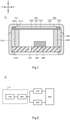
- Fig. 1 shows a detection sensor S according to the first embodiment.
- Fig. 1 shows a Z-Z' direction (first direction) and an X-X' direction (second direction).
- the Z-Z' direction includes a Z direction (one side in the first direction) and a Z' direction (the other side in the first direction).
- the X-X' direction is substantially orthogonal to the Z-Z' direction and includes an X direction and an X' direction.
- the detection sensor S includes a vibratable film 100.
- the vibratable film 100 is constituted by a piezoelectric film exhibiting pyroelectricity.
- the vibratable film 100 includes a film body 110, a first electrode 120, and a second electrode 130.
- the film body 110 may be a synthetic resin film having a dimension in the Z-Z' direction (thickness dimension) of about 0.015 mm to about 0.030 mm, for example.
- the film body 110 has a first face on the Z-direction side and a second face on the Z'-direction side.
- the first electrode 120 is provided on the first face of the film body 110.
- the second electrode 130 is provided on the second face of the film body 110.
- the Z-Z' direction is the thickness direction of the vibratable film 100.
- the vibratable film 100 is configured to be irradiated with infrared rays and thereby generate first electric signals through a pyroelectric effect. Specifically, the vibratable film 100 is spontaneously polarized when not irradiated with infrared rays. When the vibratable film 100 is irradiated with infrared rays resulting in a change in temperature of the vibratable film 100, the spontaneous polarization of the vibratable film 100 accordingly changes to cause a change in voltage of the vibratable film 100, i.e., to generate the first electric signals.
- the vibratable film 100 is further configured to be vibrated by sound waves and thereby generate second electric signals through a piezoelectric effect. Specifically, the vibratable film 100 is configured to be deformed by vibration and accordingly cause changes in voltage, i.e., generate the second electric signals.
- the detection sensor S further includes a case 200.
- the case 200 accommodates the vibratable film 100.
- the case 200 includes a case body 210 and a transmissive part 220.
- the case body 210 includes a top plate 211 and a tubular portion 212.
- the top plate 211 is disposed on the Z-direction side relative to the vibratable film 100.
- the top plate 211 has an opening 211a passing through the top plate 211 in the Z-Z' direction.
- the tubular portion 212 extends in the Z' direction from the perimeter portion of the top plate 211.
- the tubular portion 212 has an end portion 212a on the Z' direction side.
- the end portion 212a may be bent generally in a L-shape or may extend in the Z-Z' direction.
- the transmissive part 220 is fitted in the opening 211a. Accordingly, in a cross section along the X-X' direction, the transmissive part 220 has an outer shape that is substantially the same as the shape of the opening 211a, and has outer dimensions that are the same as, or slightly larger than, the dimensions of the opening 211a.
- the transmissive part 220 is disposed on the Z-direction side relative to the vibratable film 100 to face the vibratable film 100.
- the transmissive part 220 is configured to transmit at least infrared rays.
- the transmissive part 220 may be constituted by an optical filter configured to transmit infrared rays in a predetermined wavelength band only (for example, 1.2 ⁇ m to 1.4 ⁇ m (1200 nm to 1400 nm)), an optical filter configured to transmit infrared rays in a wavelength band of 780 nm to 1 mm, or an optical filter configured to transmit infrared rays and light in a wavelength band or bands near the infrared band (for example, visible light of a wavelength band from about 400 nm to 780 nm and/or microwaves having a wavelength band from 1 mm to 1m).
- the optical filter may be constituted by an optical lens made of silicon, for example, but is not limited thereto.
- the transmissive part 220 may be composed of a transparent or translucent material, such as synthetic resin or glass, configured to transmit at least infrared rays. Infrared rays having transmitted through the transmissive part 220 of any of the above aspects are projected onto the vibratable film 100.
- the detection sensor S further includes a circuit board 300.
- the circuit board 300 is fixed to the case 200.
- the circuit board 300 may be fixed to the end portion 212a bent generally in a L-shape of the tubular portion 212 of the case 200 (see Fig. 1 ); the end portion 212a extending in the Z-Z' direction of the tubular portion 212 of the case 200 may be securely received in, and thereby fixed to, an engagement hole of the circuit board 300 (not shown); or the end portion 212a extending in the Z-Z' direction of the tubular portion 212 of the case 200 may be bonded to, and thereby fixed to, the circuit board 300 with a conductive adhesive or the like (not shown).
- the circuit board 300 is disposed on the Z'-direction side relative to, and in spaced relation to, the vibratable film 100.
- the circuit board 300 includes a sound hole 310.
- the sound hole 310 extends through the circuit board 300 in the Z-Z' direction.
- the sound hole 310 In a cross section along the X-X' direction, the sound hole 310 has a shape that is the same as, or different from, the outer shape of the transmissive part 220.
- the sound hole 310 In a cross section along the X-X' direction, the sound hole 310 may have dimensions that are smaller than the outer dimensions of the transmissive part 220, but is not limited thereto.
- the sound hole 310 may have a dimension (a diameter) between 0.6 mm and 0.8 mm in a cross section along the X-X' direction.
- the sound hole 310 may face the vibratable film 100, or there may be another member interposed between the sound hole 310 and the vibratable film 100. Sound waves inputted through the sound hole 310 are to vibrate the vibratable film 100.
- a waterproof and/or dustproof sheet (not shown) may be fixed to the circuit board 300 from the Z'-direction side to close the sound hole 310 from the Z'-direction side. This sheet can be omitted.
- the detection sensor S may further include a field effect transistor 400 (FET 400).
- FET 400 is electrically connected to the vibratable film 100.
- the FET 400 may be mounted on the circuit board 300, or may be mounted on another circuit board (not shown) electrically connected to the circuit board 300.
- the FET 400 is configured to receive the first signals and/or the second electric signals from the vibratable film 100 and perform impedance conversion on the first electric signals and/or the second electric signals to output the converted first electric signals and/or the converted second electric signals as output signals.
- the detection sensor S may further include a conductive ring 500 and a gate ring 600 of a tubular shape.
- the conductive ring 500 is interposed between the perimeter portion of the vibratable film 100 and the top plate 211 of the case 200, and is in contact with the first electrode 120 of the vibratable film 100.
- the case body 210 of the case 200 is made of an electrically conductive material.
- the gate ring 600 is electrically conductive, interposed between the perimeter portion of the vibratable film 100 and the circuit board 300, and in contact with the second electrode 130 of the vibratable film 100.
- the first electrode 120 of the vibratable film 100 is electrically connected to the FET 400 via the conductive ring 500, the case body 210, and the circuit board 300, while the second electrode 130 of the vibratable film 100 is electrically connected to the FET 400 via the gate ring 600 and the circuit board 300.
- the FET 400 is thus electrically connected to the vibratable film 100.
- the detection sensor S may further include a holder 700 of a tubular shape.
- the holder 700 is electrically insulative.
- the holder 700 is disposed between the gate ring 600 and the tubular portion 212 of the case body 210. Accordingly, in a cross section along the X-X' direction, the holder 700 has an inner shape that is the same as the outer shape of the gate ring 600, and has inner dimensions that are substantially the same as, or slightly larger than, the outer dimensions of the gate ring 600.
- the holder 700 has an outer shape that is the same as the inner shape of the tubular portion 212 of the case body 210, and has outer dimensions that are substantially the same as, or slightly smaller than, the inner dimensions of the tubular portion 212 of the case body 210.
- the holder 700 may or may not be in contact with a portion of the vibratable film 100 that is outside the portion of the vibratable film 100 that is contacted by the gate ring 600. Also, the holder 700 may or may not be in contact with the circuit board 300.
- Fig. 2 shows the detection device D according to the first embodiment.
- the detection device D may include the detection sensor S according to one of the above aspects, a low-pass filter 810, and a high-pass filter 820.
- the low-pass filter 810 may be provided on a circuit board (not shown) electrically connected to the circuit board 300, or on the circuit board 300.
- the low-pass filter 810 is electrically connected to the FET 400 via the circuit board 300 and configured to receive output signals from the FET 400.
- the low-pass filter 810 is configured to pass signals within a frequency band (first frequency band), which signals within the first frequency band are obtained by impedance converting the first electric signals, out of the received output signals.
- the low-pass filter 810 is also configured to attenuate signals in a frequency band higher than the first frequency band (the frequency band signals of which can pass through the low-pass filter 810).
- signals obtained by impedance converting the first electric signals falls within a frequency band between 0.35 Hz and 5.0 Hz, and accordingly the low-pass filter 810 is configured to pass signals in a frequency band of 5.0 Hz and lower, out of the received output signals, and to attenuate signals in a frequency band of higher than 5.0 Hz (not including 5.0 Hz).
- the high-pass filter 820 may be provided on a circuit board (not shown) electrically connected to the circuit board 300, or on the circuit board 300.
- the high-pass filter 820 is electrically connected to the FET 400 via the circuit board 300 and configured to receive output signals from the FET 400.
- the high-pass filter 820 is configured to pass signals in a frequency band (second frequency band) higher than the first frequency band (the frequency band signals of which can pass through the low-pass filter 810), out of the received output signals.
- the high-pass filter 820 is also configured to attenuate signals in a frequency band lower than the second frequency band (the frequency band signals of which can pass through the high-pass filter 820).
- the high-pass filter 820 is configured to pass signals in a frequency band higher than 10.0 Hz (not including 10.0 Hz) and attenuate signals in a frequency band of 10.0 Hz and lower.
- the detection device D may further include a controller 830.
- the controller 830 may be provided on a circuit board (not shown) electrically connected to the circuit board 300, or on the circuit board 300.
- the controller 830 is electrically connected to the low-pass filter 810 and the high-pass filter 820, and configured to receive signals that have passed through the low-pass filter 810 and signals that have passed through the high-pass filter 820.
- the controller 830 may be, but is not required to be, electrically connected to the FET 400 to receive output signals from the FET 400.
- the controller 830 may be configured to determine whether or not the controller 830 has received signals only from the low-pass filter 810.
- the controller 830 determines whether or not it has received signals from the low-pass filter 810 (first determination). If the controller 830 determines that it has received signals from the low-pass filter 810, the controller 830 counts for a predetermined period, using a timer circuit in the controller 830 or a software timer on an internal memory, and determines whether or not it has received signals from the high-pass filter 820 within the predetermined period (second determination).
- the controller 830 determines that it has received signals from the high-pass filter 820 within the predetermined period (that is, if the controller 830 determines that it has received signals not only from the low-pass filter 810), the controller 830 returns to the processing of the first determination. On the other hand, if the controller 830 determines that it has not received any signals from the high-pass filter 820 within the predetermined period, then the controller 830 determines that it has received signals only from the low-pass filter 810. In this example configuration, the controller 830 is configured to make the second determination within the predetermined period after making the first determination. Instead, the controller 830 may be configured to make the first determination within the predetermined period after making the second determination.
- the controller 830 determines that it has received signals only from the low-pass filter 810, this means that the controller 830 has received signals obtained by impedance converting the first electric signals from the vibratable film 100 by irradiating the vibratable film 100 with infrared rays. Thus the controller 830 determines that infrared rays have fallen on the vibratable film 100 and thereby is able to detect the infrared rays. If the controller 830 determines that it has received signals not only from the low-pass filter 810, this means that the controller 830 has received signals obtained by impedance converting the second electric signals from the vibratable film 100 vibrated by sound waves. Thus the controller 830 determines that the vibratable film 100 is vibrated by the sound waves and thereby is able to detect the sound waves.
- the controller 830 may be further configured such that if the controller 830 determines that it has received signals only from the low-pass filter 810, the controller 830 performs signal processing, such as voice recognition processing, on signals received from the FET 400, or alternatively on signals received from the low-pass filter 810 and signals received from the high-pass filter 820.
- the controller 830 may be configured to amplify signals received from the FET 400, or alternatively signals received from the low-pass filter 810 and signals received from the high-pass filter 820, and perform the above-described signal processing on the amplified signals.
- the controller 830 may be configured to return to the first determination on the basis of externally provided instruction information.
- the controller 830 may be configured such that if the controller 830 determines that it has received signals only from the low-pass filter 810, the controller 830 counts for a predetermined period, using a timer circuit in the controller 830 or a software timer on an internal memory, and perform signal processing within the predetermined period in one of the above manners.
- the controller 830 may be configured to return to the processing of the first determination after the predetermined period has elapsed.
- the controller 830 may not include the configuration for performing the above signal processing and may be configured to repeat the processing of the first determination and the processing of the second determination in this order or in the reverse order.
- the detection sensor S and the detection device D described above provide at least the following technical features and effects.
- Technical Feature and Effect (1) the detection sensor S is resistant to entry of dirt, dust, and/or water through the sound hole for the following reasons.
- the detection sensor S and the detection device D are configured to allow infrared rays to enter the case 200 through the transmissive part 220 of the case 200. As such, the case 200 has no opening for taking in infrared rays into the detection sensor S.
- the circuit board 300 is provided with the sound hole 310, but this hole is small in size. Therefore, the detection sensor S is resistant to entry of dirt, dust, and/or water into through the sound hole 310. Where the sound hole 310 is closed with the waterproof and/or dustproof sheet, the detection sensor S is further resistant to entry of dirt, dust, and/or water through the sound hole 310.
- the detection sensor S and the detection device D has improved versatility for the following reasons. Since the detection sensor S is dustproof and/or waterproof as described above, the detection sensor S can be installed in a place with a lot of dust and dirt and/or a place where water may adhere. Also, human bodies emit infrared rays having a peak wavelength of about 10 ⁇ m (1000 nm). Since the emitted infrared rays are transmitted through the transmissive part 220 of the detection sensor S of the detection device D and are projected onto the vibratable film 100, the detection device D may detect approach of a human body (including placing a hand of a human over the detection device D) in a manner as described above.
- the detection device D may be incorporated in a vending machine or a ticket machine, for example.
- the detection device D of this aspect may be configured to perform voice recognition processing after detecting approach of a human body by detecting irradiated infrared rays on the vibratable film 100 as described above.
- the vending machine or the ticket machine may allow the human to purchase a product by his or her voice without touching the vending machine or the ticket machine with the human body.
- the detection device D may be incorporated in a fire detector, for example.
- the detection device D of this aspect may be configured to perform voice recognition processing after detecting a temperature change caused by a fire or other causes, by detecting irradiated infrared rays on the vibratable film 100 as described above. In this case, after detecting a temperature change caused by a fire or other causes, the fire detector may transmit processed voice data through the Internet or other lines.
- the detection device D may be incorporated in a security camera or other alarm devices.
- the detection device D of this aspect may be configured to perform voice recognition processing after detecting approach of a human body by detecting irradiated infrared rays on the vibratable film 100 as described above. In this case, after detecting approach of a human, the alarm device may record processed voice data (voices, sounds, etc.) and/or transmit the processed voice data through the Internet or other lines.
- the detection sensor S has a reduced number of components for the following reasons. Since the vibratable film 100 is formed using a piezoelectric film exhibiting pyroelectricity, the detection sensor S does not require both a piezoelectric film and a pyroelectric film like the detection sensor of the conventional example discussed above. In addition, the single FET 400 is capable of performing impedance conversion on both the first electric signals and second electric signals from the vibratable film 100, the detection sensor S does not require two FETs like the detection sensor of the conventional example discussed above.
- the detection sensor S is structured such that the transmissive part 220 is provided in the case 200, and the sound hole 310 is provided in the circuit board 300.
- the detection sensor of the invention may be structured as in a detection sensor S' shown in Fig. 3 . More particularly, a transmissive part 320 is provided in a circuit board 300', and a sound hole 230 is provided in a top plate 211 of a case 200'.
- the detection sensor S' has substantially the same configuration as the detection sensor S except the following points.
- the transmissive part 320 is disposed on the Z' direction side relative to, and in spaced relation to, the vibratable film 100 to face the vibratable film 100.
- the detection device D may include the detection sensor S' in place of the detection sensor S.
- the detection sensors S and S' of any of the above aspects are not limited to those provided in the detection device D, but may be provided in other detection devices or electronic devices for use.
Landscapes
- Physics & Mathematics (AREA)
- General Physics & Mathematics (AREA)
- Spectroscopy & Molecular Physics (AREA)
- Engineering & Computer Science (AREA)
- Power Engineering (AREA)
- Photometry And Measurement Of Optical Pulse Characteristics (AREA)
Abstract
Description
- The invention relates to detection sensors and detection devices including the same.
- A conventional detection sensor is described in
Japanese Published Unexamined Utility Model Application No. S56-48189 - The above conventional detection sensor receives infrared rays and sound waves through the common opening, which is wide open to take in infrared rays. Therefore, the opening easily allows dirt, dust, and/or water to enter therethrough into the conventional detection sensor.
- The invention provides a detection sensor resisting entry of dirt, dust, and/or water. The invention also provides a detection device including the detection sensor.
- A detection sensor according to an aspect of the invention includes a vibratable film constituted by a piezoelectric film, a case accommodating the vibratable film, and a circuit board. The vibratable film is configured to be irradiated with infrared rays and thereby generate first electric signals through a pyroelectric effect, and configured to be vibrated by sound waves and thereby generate second electric signals through a piezoelectric effect. The case includes a transmissive part. The transmissive part is configured to transmit at least infrared rays and disposed on one side in a first direction relative to the vibratable film to face the vibratable film. The first direction is a thickness direction of the vibratable film. The circuit board is fixed to the case and disposed on the other side in the first direction relative to the vibratable film. The circuit board has a sound hole to input therethrough sound waves.
- The transmissive part may be provided not in the case but in the circuit board and disposed on the other side in the first direction relative to the vibratable film. In this case, the sound hole may be provided not in the circuit board but in a top plate of the case.
- The detection sensor of either of the above aspects resistant to entry of dirt, dust, and/or water for the following reasons. The detection sensor is configured such that the vibratable film is irradiated with infrared rays passing through the transmissive part. As such, the detection sensor has no opening for taking in infrared rays into the detection sensor. The circuit board or the case is provided with the sound hole, but this hole is small in size. Therefore, dirt, dust, and/or water is unlikely to enter the detection sensor through the sound hole.
- In a cross section along a second direction substantially orthogonal to the first direction, the sound hole may have dimensions that are smaller than the dimensions of the transmissive part.
- The transmissive part may be constituted by an optical filter configured to transmit infrared rays in a predetermined wavelength band.
- The vibratable film may include a film body and first and second electrodes. The film body may have a first face on the one side in the first direction and a second face on the other side in the first direction. The first electrode may be provided on the first face of the film body. The second electrode may be provided on the second face of the film body.
- The detection sensor of any of the above aspects may further include a field effect transistor. The field effect transistor may be configured to perform impedance conversion on the first electric signals and/or the second electric signals received from the vibratable film and output the converted first electric signals and/or the converted second electric signals as output signals.
- A detection device according to an aspect of the invention may include the detection sensor according to one of the above aspects, a low-pass filter, and a high-pass filter. The low-pass filter may be configured to receive the output signals from the field effect transistor, to pass signals within a frequency band obtained by impedance converting the first electric signals out of the received output signals, and to attenuate signals in a frequency band higher than the frequency band of the signals capable of passing through the low-pass filter. The high-pass filter may be configured to pass signals in a frequency band out of the output signals, the frequency band being higher than the frequency band of the signals capable of passing through the low-pass filter, and to attenuate signals in a frequency band lower than the frequency band of the signals capable of passing through the high-pass filter.
- The detection device may further include a controller. The controller may be configured to receive the signals that have passed through the low-pass filter and the signals that have passed through the high-pass filter, and to determine whether or not the controller has received signals only from the low-pass filter.
- The controller may be further configured such that if the controller determines that the controller has received signals only from the low-pass filter, then the controller performs signal processing on the output signals from the field effect transistor, or alternatively on the signals that have passed through the low-pass filter and the signals that have passed through the high-pass filter.
-
-
Fig. 1 is a schematic cross-sectional view of a detection sensor according to a first embodiment of the invention. -
Fig. 2 is a block diagram of a detection device according to the first embodiment of the invention. -
Fig. 3 is a schematic cross-sectional view of a variant of the detection sensor. - In the brief description of the drawings above and the description of embodiments which follows, relative spatial terms such as "upper", "lower", "top", "bottom", "left", "right", "front", "rear", etc., are used for the convenience of the skilled reader and refer to the orientation of the detection sensors, detection devices, and their constituent parts as depicted in the drawings. No limitation is intended by use of these terms, either in use of the invention, during its manufacture, shipment, custody, or sale, or during assembly of its constituent parts or when incorporated into or combined with other apparatus.
- A first embodiment of the invention and design modifications thereof will now be described. It should be noted that constituents of the embodiments and the modifications thereof to be described may be combined in any possible manner. Materials, shapes, dimensions, numbers, arrangements, etc. of the constituents of the various aspects of the embodiments and the modifications thereof will be discussed below as examples only and may be modified as long as they achieve similar functions.
- Hereinafter described is a detection sensor S according to a plurality of embodiments, including a first embodiment, of the invention with reference to
Fig. 1. Fig. 1 shows a detection sensor S according to the first embodiment.Fig. 1 shows a Z-Z' direction (first direction) and an X-X' direction (second direction). The Z-Z' direction includes a Z direction (one side in the first direction) and a Z' direction (the other side in the first direction). The X-X' direction is substantially orthogonal to the Z-Z' direction and includes an X direction and an X' direction. - The detection sensor S includes a
vibratable film 100. Thevibratable film 100 is constituted by a piezoelectric film exhibiting pyroelectricity. Thevibratable film 100 includes afilm body 110, afirst electrode 120, and asecond electrode 130. Thefilm body 110 may be a synthetic resin film having a dimension in the Z-Z' direction (thickness dimension) of about 0.015 mm to about 0.030 mm, for example. Thefilm body 110 has a first face on the Z-direction side and a second face on the Z'-direction side. Thefirst electrode 120 is provided on the first face of thefilm body 110. Thesecond electrode 130 is provided on the second face of thefilm body 110. The Z-Z' direction is the thickness direction of thevibratable film 100. - The
vibratable film 100 is configured to be irradiated with infrared rays and thereby generate first electric signals through a pyroelectric effect. Specifically, thevibratable film 100 is spontaneously polarized when not irradiated with infrared rays. When thevibratable film 100 is irradiated with infrared rays resulting in a change in temperature of thevibratable film 100, the spontaneous polarization of thevibratable film 100 accordingly changes to cause a change in voltage of thevibratable film 100, i.e., to generate the first electric signals. - The
vibratable film 100 is further configured to be vibrated by sound waves and thereby generate second electric signals through a piezoelectric effect. Specifically, thevibratable film 100 is configured to be deformed by vibration and accordingly cause changes in voltage, i.e., generate the second electric signals. - The detection sensor S further includes a
case 200. Thecase 200 accommodates thevibratable film 100. Thecase 200 includes acase body 210 and atransmissive part 220. Thecase body 210 includes atop plate 211 and atubular portion 212. Thetop plate 211 is disposed on the Z-direction side relative to thevibratable film 100. Thetop plate 211 has anopening 211a passing through thetop plate 211 in the Z-Z' direction. Thetubular portion 212 extends in the Z' direction from the perimeter portion of thetop plate 211. Thetubular portion 212 has anend portion 212a on the Z' direction side. Theend portion 212a may be bent generally in a L-shape or may extend in the Z-Z' direction. - The
transmissive part 220 is fitted in theopening 211a. Accordingly, in a cross section along the X-X' direction, thetransmissive part 220 has an outer shape that is substantially the same as the shape of theopening 211a, and has outer dimensions that are the same as, or slightly larger than, the dimensions of theopening 211a. Thetransmissive part 220 is disposed on the Z-direction side relative to thevibratable film 100 to face thevibratable film 100. Thetransmissive part 220 is configured to transmit at least infrared rays. For example, thetransmissive part 220 may be constituted by an optical filter configured to transmit infrared rays in a predetermined wavelength band only (for example, 1.2 µm to 1.4 µm (1200 nm to 1400 nm)), an optical filter configured to transmit infrared rays in a wavelength band of 780 nm to 1 mm, or an optical filter configured to transmit infrared rays and light in a wavelength band or bands near the infrared band (for example, visible light of a wavelength band from about 400 nm to 780 nm and/or microwaves having a wavelength band from 1 mm to 1m). The optical filter may be constituted by an optical lens made of silicon, for example, but is not limited thereto. In place of the optical filter, thetransmissive part 220 may be composed of a transparent or translucent material, such as synthetic resin or glass, configured to transmit at least infrared rays. Infrared rays having transmitted through thetransmissive part 220 of any of the above aspects are projected onto thevibratable film 100. - The detection sensor S further includes a
circuit board 300. Thecircuit board 300 is fixed to thecase 200. For example, thecircuit board 300 may be fixed to theend portion 212a bent generally in a L-shape of thetubular portion 212 of the case 200 (seeFig. 1 ); theend portion 212a extending in the Z-Z' direction of thetubular portion 212 of thecase 200 may be securely received in, and thereby fixed to, an engagement hole of the circuit board 300 (not shown); or theend portion 212a extending in the Z-Z' direction of thetubular portion 212 of thecase 200 may be bonded to, and thereby fixed to, thecircuit board 300 with a conductive adhesive or the like (not shown). Thecircuit board 300 is disposed on the Z'-direction side relative to, and in spaced relation to, thevibratable film 100. - The
circuit board 300 includes asound hole 310. Thesound hole 310 extends through thecircuit board 300 in the Z-Z' direction. In a cross section along the X-X' direction, thesound hole 310 has a shape that is the same as, or different from, the outer shape of thetransmissive part 220. In a cross section along the X-X' direction, thesound hole 310 may have dimensions that are smaller than the outer dimensions of thetransmissive part 220, but is not limited thereto. For example, thesound hole 310 may have a dimension (a diameter) between 0.6 mm and 0.8 mm in a cross section along the X-X' direction. Thesound hole 310 may face thevibratable film 100, or there may be another member interposed between thesound hole 310 and thevibratable film 100. Sound waves inputted through thesound hole 310 are to vibrate thevibratable film 100. A waterproof and/or dustproof sheet (not shown) may be fixed to thecircuit board 300 from the Z'-direction side to close thesound hole 310 from the Z'-direction side. This sheet can be omitted. - The detection sensor S may further include a field effect transistor 400 (FET 400). The
FET 400 is electrically connected to thevibratable film 100. TheFET 400 may be mounted on thecircuit board 300, or may be mounted on another circuit board (not shown) electrically connected to thecircuit board 300. TheFET 400 is configured to receive the first signals and/or the second electric signals from thevibratable film 100 and perform impedance conversion on the first electric signals and/or the second electric signals to output the converted first electric signals and/or the converted second electric signals as output signals. - The detection sensor S may further include a
conductive ring 500 and agate ring 600 of a tubular shape. Theconductive ring 500 is interposed between the perimeter portion of thevibratable film 100 and thetop plate 211 of thecase 200, and is in contact with thefirst electrode 120 of thevibratable film 100. In this case, thecase body 210 of thecase 200 is made of an electrically conductive material. Thegate ring 600 is electrically conductive, interposed between the perimeter portion of thevibratable film 100 and thecircuit board 300, and in contact with thesecond electrode 130 of thevibratable film 100. Thefirst electrode 120 of thevibratable film 100 is electrically connected to theFET 400 via theconductive ring 500, thecase body 210, and thecircuit board 300, while thesecond electrode 130 of thevibratable film 100 is electrically connected to theFET 400 via thegate ring 600 and thecircuit board 300. TheFET 400 is thus electrically connected to thevibratable film 100. - The detection sensor S may further include a
holder 700 of a tubular shape. Theholder 700 is electrically insulative. Theholder 700 is disposed between thegate ring 600 and thetubular portion 212 of thecase body 210. Accordingly, in a cross section along the X-X' direction, theholder 700 has an inner shape that is the same as the outer shape of thegate ring 600, and has inner dimensions that are substantially the same as, or slightly larger than, the outer dimensions of thegate ring 600. Also, in a cross section along the X-X' direction, theholder 700 has an outer shape that is the same as the inner shape of thetubular portion 212 of thecase body 210, and has outer dimensions that are substantially the same as, or slightly smaller than, the inner dimensions of thetubular portion 212 of thecase body 210. Theholder 700 may or may not be in contact with a portion of thevibratable film 100 that is outside the portion of thevibratable film 100 that is contacted by thegate ring 600. Also, theholder 700 may or may not be in contact with thecircuit board 300. - Hereinafter described is a detection device D according to a plurality of embodiments, including a first embodiment, of the invention with reference to
Fig. 2. Fig. 2 shows the detection device D according to the first embodiment. - The detection device D may include the detection sensor S according to one of the above aspects, a low-
pass filter 810, and a high-pass filter 820. - The low-
pass filter 810 may be provided on a circuit board (not shown) electrically connected to thecircuit board 300, or on thecircuit board 300. The low-pass filter 810 is electrically connected to theFET 400 via thecircuit board 300 and configured to receive output signals from theFET 400. The low-pass filter 810 is configured to pass signals within a frequency band (first frequency band), which signals within the first frequency band are obtained by impedance converting the first electric signals, out of the received output signals. The low-pass filter 810 is also configured to attenuate signals in a frequency band higher than the first frequency band (the frequency band signals of which can pass through the low-pass filter 810). Specifically, signals obtained by impedance converting the first electric signals falls within a frequency band between 0.35 Hz and 5.0 Hz, and accordingly the low-pass filter 810 is configured to pass signals in a frequency band of 5.0 Hz and lower, out of the received output signals, and to attenuate signals in a frequency band of higher than 5.0 Hz (not including 5.0 Hz). - The high-
pass filter 820 may be provided on a circuit board (not shown) electrically connected to thecircuit board 300, or on thecircuit board 300. The high-pass filter 820 is electrically connected to theFET 400 via thecircuit board 300 and configured to receive output signals from theFET 400. The high-pass filter 820 is configured to pass signals in a frequency band (second frequency band) higher than the first frequency band (the frequency band signals of which can pass through the low-pass filter 810), out of the received output signals. The high-pass filter 820 is also configured to attenuate signals in a frequency band lower than the second frequency band (the frequency band signals of which can pass through the high-pass filter 820). Specifically, the high-pass filter 820 is configured to pass signals in a frequency band higher than 10.0 Hz (not including 10.0 Hz) and attenuate signals in a frequency band of 10.0 Hz and lower. - The detection device D may further include a
controller 830. Thecontroller 830 may be provided on a circuit board (not shown) electrically connected to thecircuit board 300, or on thecircuit board 300. Thecontroller 830 is electrically connected to the low-pass filter 810 and the high-pass filter 820, and configured to receive signals that have passed through the low-pass filter 810 and signals that have passed through the high-pass filter 820. Thecontroller 830 may be, but is not required to be, electrically connected to theFET 400 to receive output signals from theFET 400. - The
controller 830 may be configured to determine whether or not thecontroller 830 has received signals only from the low-pass filter 810. Hereinafter described is a non-limiting example configuration of thecontroller 830. Thecontroller 830 determines whether or not it has received signals from the low-pass filter 810 (first determination). If thecontroller 830 determines that it has received signals from the low-pass filter 810, thecontroller 830 counts for a predetermined period, using a timer circuit in thecontroller 830 or a software timer on an internal memory, and determines whether or not it has received signals from the high-pass filter 820 within the predetermined period (second determination). If thecontroller 830 determines that it has received signals from the high-pass filter 820 within the predetermined period (that is, if thecontroller 830 determines that it has received signals not only from the low-pass filter 810), thecontroller 830 returns to the processing of the first determination. On the other hand, if thecontroller 830 determines that it has not received any signals from the high-pass filter 820 within the predetermined period, then thecontroller 830 determines that it has received signals only from the low-pass filter 810. In this example configuration, thecontroller 830 is configured to make the second determination within the predetermined period after making the first determination. Instead, thecontroller 830 may be configured to make the first determination within the predetermined period after making the second determination. - If the
controller 830 determines that it has received signals only from the low-pass filter 810, this means that thecontroller 830 has received signals obtained by impedance converting the first electric signals from thevibratable film 100 by irradiating thevibratable film 100 with infrared rays. Thus thecontroller 830 determines that infrared rays have fallen on thevibratable film 100 and thereby is able to detect the infrared rays. If thecontroller 830 determines that it has received signals not only from the low-pass filter 810, this means that thecontroller 830 has received signals obtained by impedance converting the second electric signals from thevibratable film 100 vibrated by sound waves. Thus thecontroller 830 determines that thevibratable film 100 is vibrated by the sound waves and thereby is able to detect the sound waves. - The
controller 830 may be further configured such that if thecontroller 830 determines that it has received signals only from the low-pass filter 810, thecontroller 830 performs signal processing, such as voice recognition processing, on signals received from theFET 400, or alternatively on signals received from the low-pass filter 810 and signals received from the high-pass filter 820. Thecontroller 830 may be configured to amplify signals received from theFET 400, or alternatively signals received from the low-pass filter 810 and signals received from the high-pass filter 820, and perform the above-described signal processing on the amplified signals. - The
controller 830 may be configured to return to the first determination on the basis of externally provided instruction information. Alternatively, thecontroller 830 may be configured such that if thecontroller 830 determines that it has received signals only from the low-pass filter 810, thecontroller 830 counts for a predetermined period, using a timer circuit in thecontroller 830 or a software timer on an internal memory, and perform signal processing within the predetermined period in one of the above manners. In this case, thecontroller 830 may be configured to return to the processing of the first determination after the predetermined period has elapsed. Thecontroller 830 may not include the configuration for performing the above signal processing and may be configured to repeat the processing of the first determination and the processing of the second determination in this order or in the reverse order. - The detection sensor S and the detection device D described above provide at least the following technical features and effects. Technical Feature and Effect (1): the detection sensor S is resistant to entry of dirt, dust, and/or water through the sound hole for the following reasons. The detection sensor S and the detection device D are configured to allow infrared rays to enter the
case 200 through thetransmissive part 220 of thecase 200. As such, thecase 200 has no opening for taking in infrared rays into the detection sensor S. Thecircuit board 300 is provided with thesound hole 310, but this hole is small in size. Therefore, the detection sensor S is resistant to entry of dirt, dust, and/or water into through thesound hole 310. Where thesound hole 310 is closed with the waterproof and/or dustproof sheet, the detection sensor S is further resistant to entry of dirt, dust, and/or water through thesound hole 310. - Technical Feature and Effect (2): The detection sensor S and the detection device D has improved versatility for the following reasons. Since the detection sensor S is dustproof and/or waterproof as described above, the detection sensor S can be installed in a place with a lot of dust and dirt and/or a place where water may adhere. Also, human bodies emit infrared rays having a peak wavelength of about 10 µm (1000 nm). Since the emitted infrared rays are transmitted through the
transmissive part 220 of the detection sensor S of the detection device D and are projected onto thevibratable film 100, the detection device D may detect approach of a human body (including placing a hand of a human over the detection device D) in a manner as described above. The detection device D may be incorporated in a vending machine or a ticket machine, for example. The detection device D of this aspect may be configured to perform voice recognition processing after detecting approach of a human body by detecting irradiated infrared rays on thevibratable film 100 as described above. In this case, after detecting an approach of a human, the vending machine or the ticket machine may allow the human to purchase a product by his or her voice without touching the vending machine or the ticket machine with the human body. The detection device D may be incorporated in a fire detector, for example. The detection device D of this aspect may be configured to perform voice recognition processing after detecting a temperature change caused by a fire or other causes, by detecting irradiated infrared rays on thevibratable film 100 as described above. In this case, after detecting a temperature change caused by a fire or other causes, the fire detector may transmit processed voice data through the Internet or other lines. The detection device D may be incorporated in a security camera or other alarm devices. The detection device D of this aspect may be configured to perform voice recognition processing after detecting approach of a human body by detecting irradiated infrared rays on thevibratable film 100 as described above. In this case, after detecting approach of a human, the alarm device may record processed voice data (voices, sounds, etc.) and/or transmit the processed voice data through the Internet or other lines. - Technical Feature and Effect (3): The detection sensor S has a reduced number of components for the following reasons. Since the
vibratable film 100 is formed using a piezoelectric film exhibiting pyroelectricity, the detection sensor S does not require both a piezoelectric film and a pyroelectric film like the detection sensor of the conventional example discussed above. In addition, thesingle FET 400 is capable of performing impedance conversion on both the first electric signals and second electric signals from thevibratable film 100, the detection sensor S does not require two FETs like the detection sensor of the conventional example discussed above. - It should be appreciated that the detection sensor and the detection device described above are not limited to the embodiments described above, but may be modified as appropriate within the scope of the claims. Some example modifications are described below.
- As described above, the detection sensor S is structured such that the
transmissive part 220 is provided in thecase 200, and thesound hole 310 is provided in thecircuit board 300. However, the detection sensor of the invention may be structured as in a detection sensor S' shown inFig. 3 . More particularly, atransmissive part 320 is provided in a circuit board 300', and asound hole 230 is provided in atop plate 211 of a case 200'. The detection sensor S' has substantially the same configuration as the detection sensor S except the following points. Thetransmissive part 320 is disposed on the Z' direction side relative to, and in spaced relation to, thevibratable film 100 to face thevibratable film 100. The detection device D may include the detection sensor S' in place of the detection sensor S. The detection sensors S and S' of any of the above aspects are not limited to those provided in the detection device D, but may be provided in other detection devices or electronic devices for use. - D: detection device
- S, S': detection sensor
- 100: vibratable film
110: film body; 120: first electrode; 130: second electrode - 200,200': case
- 210: case body; 211: top plate; 211a: opening; 212: tubular portion; 212a: end portion
- 220: transmissive part
- 230: sound hole
- 300: circuit board
- 310: sound hole
- 320: transmissive part
- 400: field effect transistor (FET)
- 500: conductive ring
- 600: gate ring
- 700: holder
- 100: vibratable film
- 810: low-pass filter
- 820: high-pass filter
- 830: controller
Claims (9)
- A detection sensor (S) comprising:a vibratable film (100) constituted by a piezoelectric film, the vibratable film (100) being configured to be irradiated with infrared rays and thereby generate first electric signals through a pyroelectric effect, and configured to be vibrated by sound waves and thereby generate second electric signals through a piezoelectric effect;a case (200) accommodating the vibratable film (100) and including a transmissive part (220), the transmissive part (220) being configured to transmit at least infrared rays and disposed on one side (Z) in a first direction (Z-Z') relative to the vibratable film (100) to face the vibratable film (100), the first direction (Z-Z') being a thickness direction of the vibratable film (100); anda circuit board (300) being fixed to the case (200) and disposed on the other side (Z') in the first direction (Z-Z') relative to the vibratable film (100), the circuit board (300) having a sound hole (310) to input therethrough sound waves.
- A detection sensor (S') comprising:a vibratable film (100) constituted by a piezoelectric film, the vibratable film (100) being configured to be irradiated with infrared rays and thereby generate first electric signals through a pyroelectric effect, and configured to be vibrated by sound waves and thereby generate second electric signals through a piezoelectric effect;a case (200') accommodating the vibratable film (100) and including:a top plate (211) disposed on one side (Z) in a first direction (Z-Z') relative to the vibratable film (100), the first direction (Z-Z') being a thickness direction of the vibratable film (100), anda sound hole (230) in the top plate to input sound waves through the sound hole (230); anda circuit board (300') being fixed to the case (200'), being disposed on the other side (Z') in the first direction (Z-Z') relative to the vibratable film (100), and including a transmissive part (320), the transmissive part (320) being configured to transmit at least infrared rays and disposed on the other side (Z') in the first direction (Z-Z') relative to the vibratable film (100) to face the vibratable film (100).
- The detection sensor (S, S') according to claim 1 or 2, wherein in a cross section along a second direction (X-X') substantially orthogonal to the first direction (Z-Z'), the sound hole (310, 230) has dimensions that are smaller than the dimensions of the transmissive part (220, 320).
- The detection sensor (S, S') according to any one of claims 1 to 3, wherein the transmissive part (220, 320) is constituted by an optical filter configured to transmit infrared rays in a predetermined wavelength band.
- The detection sensor (S, S') according to any one of claims 1 to 4, wherein the vibratable film (100) includes:a film body (110) having a first face on the one side (Z) in the first direction (Z-Z') and a second face on the other side (Z') in the first direction (Z-Z');a first electrode (120) on the first face of the film body (110); anda second electrode (130) on the second face of the film body (110).
- The detection sensor (S, S') according to any one of claims 1 to 5, further comprising a field effect transistor (400) configured to perform impedance conversion on the first electric signals and/or the second electric signals received from the vibratable film (100) and output the converted first electric signals and/or the converted second electric signals as output signals.
- A detection device (D) comprising:the detection sensor (S, S') according to claim 6;a low-pass filter (810) configured to receive the output signals from the field effect transistor (400), to pass signals within a frequency band obtained by impedance converting the first electric signals out of the received output signals, and to attenuate signals in a frequency band higher than the frequency band of the signals capable of passing through the low-pass filter (810);a high-pass filter (820) configured to pass signals in a frequency band out of the output signals, the frequency band being higher than the frequency band of the signals capable of passing through the low-pass filter (810), and to attenuate signals in a frequency band lower than the frequency band of the signals capable of passing through the high-pass filter (820); anda controller (830) configured to receive the signals that have passed through the low-pass filter (810) and the signals that have passed through the high-pass filter (820), and to determine whether or not the controller (830) has received signals only from the low-pass filter (810).
- The detection device (D) according to claim 7, wherein the controller (830) is further configured such that if the controller (830) determines that the controller (830) has received signals only from the low-pass filter (810), then the controller (830) performs signal processing on the output signals from the field effect transistor (400).
- The detection device (D) according to claim 7, wherein the controller (830) is further configured such that if the controller (830) determines that the controller (830) has received signals only from the low-pass filter (810), then the controller (830) performs signal processing on the signals that have passed through the low-pass filter (810) and the signals that have passed through the high-pass filter (820).
Applications Claiming Priority (1)
| Application Number | Priority Date | Filing Date | Title |
|---|---|---|---|
| JP2020148018A JP7446957B2 (en) | 2020-09-03 | 2020-09-03 | Detection sensor and detection device equipped with the same |
Publications (2)
| Publication Number | Publication Date |
|---|---|
| EP3964808A1 true EP3964808A1 (en) | 2022-03-09 |
| EP3964808B1 EP3964808B1 (en) | 2024-04-10 |
Family
ID=77640312
Family Applications (1)
| Application Number | Title | Priority Date | Filing Date |
|---|---|---|---|
| EP21191264.7A Active EP3964808B1 (en) | 2020-09-03 | 2021-08-13 | Detection sensor and detection device including the same |
Country Status (4)
| Country | Link |
|---|---|
| US (1) | US11788881B2 (en) |
| EP (1) | EP3964808B1 (en) |
| JP (1) | JP7446957B2 (en) |
| CN (1) | CN114136344B (en) |
Families Citing this family (2)
| Publication number | Priority date | Publication date | Assignee | Title |
|---|---|---|---|---|
| CN116105856B (en) * | 2023-04-03 | 2023-09-19 | 杭州海康微影传感科技有限公司 | Infrared detector and preparation method thereof |
| JP2025038633A (en) | 2023-09-07 | 2025-03-19 | ホシデン株式会社 | Detection Sensor |
Citations (6)
| Publication number | Priority date | Publication date | Assignee | Title |
|---|---|---|---|---|
| US4258260A (en) * | 1978-05-30 | 1981-03-24 | Kureha Kagaku Kogyo Kabushiki Kaisha | Pyroelectric infrared detector |
| JPS5648189U (en) | 1979-09-20 | 1981-04-28 | ||
| WO2011159003A1 (en) * | 2010-06-17 | 2011-12-22 | 주식회사 비에스이 | Microphone |
| JP2013242172A (en) * | 2012-05-18 | 2013-12-05 | Sumitomo Heavy Ind Ltd | Ultrasonic sensor |
| JP2016099137A (en) * | 2014-11-18 | 2016-05-30 | 株式会社クレハ | Piezoelectric element, acoustic wave probe, photoacoustic device |
| US20200003627A1 (en) * | 2017-03-17 | 2020-01-02 | Fujifilm Corporation | Pyroelectric sensor |
Family Cites Families (12)
| Publication number | Priority date | Publication date | Assignee | Title |
|---|---|---|---|---|
| JPS5648189A (en) | 1979-09-27 | 1981-05-01 | Toshiba Corp | Method of forming photothyristor circuit |
| JP2005106529A (en) * | 2003-09-29 | 2005-04-21 | Hosiden Corp | Piezoelectric vibration sensor |
| US8220318B2 (en) | 2005-06-17 | 2012-07-17 | Georgia Tech Research Corporation | Fast microscale actuators for probe microscopy |
| KR100705709B1 (en) | 2006-02-13 | 2007-04-12 | 두석배 | Motion sensor using infrared sensor and piezoelectric film |
| JP4497125B2 (en) * | 2006-04-11 | 2010-07-07 | 株式会社デンソー | Collision detection device |
| JP4650383B2 (en) * | 2006-09-12 | 2011-03-16 | 株式会社デンソー | UV detector |
| JP5431694B2 (en) * | 2008-07-28 | 2014-03-05 | セイコーインスツル株式会社 | Pyroelectric infrared detector |
| EP2598255A2 (en) | 2010-07-30 | 2013-06-05 | Koninklijke Philips Electronics N.V. | Thin film ultrasound transducer |
| JP5226883B2 (en) * | 2011-02-01 | 2013-07-03 | Necトーキン株式会社 | Pyroelectric infrared sensor |
| US9606606B2 (en) * | 2013-06-03 | 2017-03-28 | Qualcomm Incorporated | Multifunctional pixel and display |
| US10302599B2 (en) | 2016-10-27 | 2019-05-28 | Infineon Technologies Ag | Photoacoustic gas detector |
| US11350219B2 (en) * | 2019-08-13 | 2022-05-31 | Skyworks Solutions, Inc. | Piezoelectric MEMS microphone |
-
2020
- 2020-09-03 JP JP2020148018A patent/JP7446957B2/en active Active
-
2021
- 2021-08-10 US US17/398,052 patent/US11788881B2/en active Active
- 2021-08-13 EP EP21191264.7A patent/EP3964808B1/en active Active
- 2021-08-23 CN CN202110967929.1A patent/CN114136344B/en active Active
Patent Citations (6)
| Publication number | Priority date | Publication date | Assignee | Title |
|---|---|---|---|---|
| US4258260A (en) * | 1978-05-30 | 1981-03-24 | Kureha Kagaku Kogyo Kabushiki Kaisha | Pyroelectric infrared detector |
| JPS5648189U (en) | 1979-09-20 | 1981-04-28 | ||
| WO2011159003A1 (en) * | 2010-06-17 | 2011-12-22 | 주식회사 비에스이 | Microphone |
| JP2013242172A (en) * | 2012-05-18 | 2013-12-05 | Sumitomo Heavy Ind Ltd | Ultrasonic sensor |
| JP2016099137A (en) * | 2014-11-18 | 2016-05-30 | 株式会社クレハ | Piezoelectric element, acoustic wave probe, photoacoustic device |
| US20200003627A1 (en) * | 2017-03-17 | 2020-01-02 | Fujifilm Corporation | Pyroelectric sensor |
Also Published As
| Publication number | Publication date |
|---|---|
| US11788881B2 (en) | 2023-10-17 |
| JP7446957B2 (en) | 2024-03-11 |
| EP3964808B1 (en) | 2024-04-10 |
| JP2022042578A (en) | 2022-03-15 |
| US20220065691A1 (en) | 2022-03-03 |
| CN114136344A (en) | 2022-03-04 |
| CN114136344B (en) | 2025-04-18 |
Similar Documents
| Publication | Publication Date | Title |
|---|---|---|
| CN109492623B (en) | Ultrasonic fingerprint identification module and display panel | |
| EP3964808B1 (en) | Detection sensor and detection device including the same | |
| US5126718A (en) | Intrusion detection system | |
| TW202026941A (en) | Ultrasound fingerprint detection and related apparatus and methods | |
| JP2003144420A (en) | Fingerprint image input device and electronic device using the same | |
| TWI684917B (en) | Panel structure | |
| TWI802871B (en) | Touch display module and under-screen fingerprint recognition module thereof | |
| KR102605920B1 (en) | Optical device for vehicle | |
| KR20220170515A (en) | Electronic device having a structure for generating sound through vibration of display | |
| TWI781594B (en) | Touch display module and under-screen fingerprint recognition module thereof | |
| AU2020283912B2 (en) | Passive acoustic fingerprint sensor | |
| US20250085167A1 (en) | Detection sensor | |
| JP2757859B2 (en) | Portable terminal | |
| JP4678252B2 (en) | Security system | |
| US20250088814A1 (en) | Acoustic output devices | |
| JPS5915181Y2 (en) | Microphone with infrared sensor | |
| JP2025177046A (en) | Touch determination system, electronic device, touch determination method, program, and manufacturing method | |
| JP2004347390A (en) | Sensor device for detecting destruction of laminated glass | |
| JP2536246Y2 (en) | Glass break detector | |
| GB2599387A (en) | A sound detection device for a motor vehicle for detecting a sound in the surroundings of the motor vehicle, as well as a corresponding detection method | |
| JPH04190120A (en) | Sound-wave detecting method | |
| JP5439960B2 (en) | Dustproof device and camera | |
| JPH08184492A (en) | Pyroelectric sensor and method for modulating pyroelectric infrared-ray detecting element |
Legal Events
| Date | Code | Title | Description |
|---|---|---|---|
| PUAI | Public reference made under article 153(3) epc to a published international application that has entered the european phase |
Free format text: ORIGINAL CODE: 0009012 |
|
| STAA | Information on the status of an ep patent application or granted ep patent |
Free format text: STATUS: THE APPLICATION HAS BEEN PUBLISHED |
|
| AK | Designated contracting states |
Kind code of ref document: A1 Designated state(s): AL AT BE BG CH CY CZ DE DK EE ES FI FR GB GR HR HU IE IS IT LI LT LU LV MC MK MT NL NO PL PT RO RS SE SI SK SM TR |
|
| STAA | Information on the status of an ep patent application or granted ep patent |
Free format text: STATUS: REQUEST FOR EXAMINATION WAS MADE |
|
| 17P | Request for examination filed |
Effective date: 20220722 |
|
| RBV | Designated contracting states (corrected) |
Designated state(s): AL AT BE BG CH CY CZ DE DK EE ES FI FR GB GR HR HU IE IS IT LI LT LU LV MC MK MT NL NO PL PT RO RS SE SI SK SM TR |
|
| GRAP | Despatch of communication of intention to grant a patent |
Free format text: ORIGINAL CODE: EPIDOSNIGR1 |
|
| STAA | Information on the status of an ep patent application or granted ep patent |
Free format text: STATUS: GRANT OF PATENT IS INTENDED |
|
| RIC1 | Information provided on ipc code assigned before grant |
Ipc: H04R 17/02 20060101ALI20231030BHEP Ipc: G01J 5/35 20220101ALI20231030BHEP Ipc: G01J 5/0875 20220101ALI20231030BHEP Ipc: G01J 5/04 20060101ALI20231030BHEP Ipc: H04R 19/00 20060101ALI20231030BHEP Ipc: H04R 17/00 20060101ALI20231030BHEP Ipc: G01J 1/00 20060101ALI20231030BHEP Ipc: H04S 1/00 20060101ALI20231030BHEP Ipc: G01H 11/08 20060101AFI20231030BHEP |
|
| INTG | Intention to grant announced |
Effective date: 20231113 |
|
| GRAS | Grant fee paid |
Free format text: ORIGINAL CODE: EPIDOSNIGR3 |
|
| GRAA | (expected) grant |
Free format text: ORIGINAL CODE: 0009210 |
|
| STAA | Information on the status of an ep patent application or granted ep patent |
Free format text: STATUS: THE PATENT HAS BEEN GRANTED |
|
| AK | Designated contracting states |
Kind code of ref document: B1 Designated state(s): AL AT BE BG CH CY CZ DE DK EE ES FI FR GB GR HR HU IE IS IT LI LT LU LV MC MK MT NL NO PL PT RO RS SE SI SK SM TR |
|
| REG | Reference to a national code |
Ref country code: GB Ref legal event code: FG4D |
|
| REG | Reference to a national code |
Ref country code: CH Ref legal event code: EP |
|
| REG | Reference to a national code |
Ref country code: DE Ref legal event code: R096 Ref document number: 602021011526 Country of ref document: DE |
|
| REG | Reference to a national code |
Ref country code: IE Ref legal event code: FG4D |
|
| REG | Reference to a national code |
Ref country code: LT Ref legal event code: MG9D |
|
| REG | Reference to a national code |
Ref country code: NL Ref legal event code: MP Effective date: 20240410 |
|
| REG | Reference to a national code |
Ref country code: AT Ref legal event code: MK05 Ref document number: 1675342 Country of ref document: AT Kind code of ref document: T Effective date: 20240410 |
|
| PG25 | Lapsed in a contracting state [announced via postgrant information from national office to epo] |
Ref country code: NL Free format text: LAPSE BECAUSE OF FAILURE TO SUBMIT A TRANSLATION OF THE DESCRIPTION OR TO PAY THE FEE WITHIN THE PRESCRIBED TIME-LIMIT Effective date: 20240410 |
|
| PG25 | Lapsed in a contracting state [announced via postgrant information from national office to epo] |
Ref country code: NL Free format text: LAPSE BECAUSE OF FAILURE TO SUBMIT A TRANSLATION OF THE DESCRIPTION OR TO PAY THE FEE WITHIN THE PRESCRIBED TIME-LIMIT Effective date: 20240410 |
|
| PG25 | Lapsed in a contracting state [announced via postgrant information from national office to epo] |
Ref country code: IS Free format text: LAPSE BECAUSE OF FAILURE TO SUBMIT A TRANSLATION OF THE DESCRIPTION OR TO PAY THE FEE WITHIN THE PRESCRIBED TIME-LIMIT Effective date: 20240810 |
|
| PG25 | Lapsed in a contracting state [announced via postgrant information from national office to epo] |
Ref country code: BG Free format text: LAPSE BECAUSE OF FAILURE TO SUBMIT A TRANSLATION OF THE DESCRIPTION OR TO PAY THE FEE WITHIN THE PRESCRIBED TIME-LIMIT Effective date: 20240410 |
|
| PG25 | Lapsed in a contracting state [announced via postgrant information from national office to epo] |
Ref country code: HR Free format text: LAPSE BECAUSE OF FAILURE TO SUBMIT A TRANSLATION OF THE DESCRIPTION OR TO PAY THE FEE WITHIN THE PRESCRIBED TIME-LIMIT Effective date: 20240410 Ref country code: FI Free format text: LAPSE BECAUSE OF FAILURE TO SUBMIT A TRANSLATION OF THE DESCRIPTION OR TO PAY THE FEE WITHIN THE PRESCRIBED TIME-LIMIT Effective date: 20240410 |
|
| PG25 | Lapsed in a contracting state [announced via postgrant information from national office to epo] |
Ref country code: GR Free format text: LAPSE BECAUSE OF FAILURE TO SUBMIT A TRANSLATION OF THE DESCRIPTION OR TO PAY THE FEE WITHIN THE PRESCRIBED TIME-LIMIT Effective date: 20240711 |
|
| PG25 | Lapsed in a contracting state [announced via postgrant information from national office to epo] |
Ref country code: PT Free format text: LAPSE BECAUSE OF FAILURE TO SUBMIT A TRANSLATION OF THE DESCRIPTION OR TO PAY THE FEE WITHIN THE PRESCRIBED TIME-LIMIT Effective date: 20240812 |
|
| PG25 | Lapsed in a contracting state [announced via postgrant information from national office to epo] |
Ref country code: ES Free format text: LAPSE BECAUSE OF FAILURE TO SUBMIT A TRANSLATION OF THE DESCRIPTION OR TO PAY THE FEE WITHIN THE PRESCRIBED TIME-LIMIT Effective date: 20240410 |
|
| PG25 | Lapsed in a contracting state [announced via postgrant information from national office to epo] |
Ref country code: AT Free format text: LAPSE BECAUSE OF FAILURE TO SUBMIT A TRANSLATION OF THE DESCRIPTION OR TO PAY THE FEE WITHIN THE PRESCRIBED TIME-LIMIT Effective date: 20240410 |
|
| PG25 | Lapsed in a contracting state [announced via postgrant information from national office to epo] |
Ref country code: PL Free format text: LAPSE BECAUSE OF FAILURE TO SUBMIT A TRANSLATION OF THE DESCRIPTION OR TO PAY THE FEE WITHIN THE PRESCRIBED TIME-LIMIT Effective date: 20240410 |
|
| PG25 | Lapsed in a contracting state [announced via postgrant information from national office to epo] |
Ref country code: LV Free format text: LAPSE BECAUSE OF FAILURE TO SUBMIT A TRANSLATION OF THE DESCRIPTION OR TO PAY THE FEE WITHIN THE PRESCRIBED TIME-LIMIT Effective date: 20240410 |
|
| PG25 | Lapsed in a contracting state [announced via postgrant information from national office to epo] |
Ref country code: PT Free format text: LAPSE BECAUSE OF FAILURE TO SUBMIT A TRANSLATION OF THE DESCRIPTION OR TO PAY THE FEE WITHIN THE PRESCRIBED TIME-LIMIT Effective date: 20240812 Ref country code: PL Free format text: LAPSE BECAUSE OF FAILURE TO SUBMIT A TRANSLATION OF THE DESCRIPTION OR TO PAY THE FEE WITHIN THE PRESCRIBED TIME-LIMIT Effective date: 20240410 Ref country code: NO Free format text: LAPSE BECAUSE OF FAILURE TO SUBMIT A TRANSLATION OF THE DESCRIPTION OR TO PAY THE FEE WITHIN THE PRESCRIBED TIME-LIMIT Effective date: 20240710 Ref country code: LV Free format text: LAPSE BECAUSE OF FAILURE TO SUBMIT A TRANSLATION OF THE DESCRIPTION OR TO PAY THE FEE WITHIN THE PRESCRIBED TIME-LIMIT Effective date: 20240410 Ref country code: IS Free format text: LAPSE BECAUSE OF FAILURE TO SUBMIT A TRANSLATION OF THE DESCRIPTION OR TO PAY THE FEE WITHIN THE PRESCRIBED TIME-LIMIT Effective date: 20240810 Ref country code: HR Free format text: LAPSE BECAUSE OF FAILURE TO SUBMIT A TRANSLATION OF THE DESCRIPTION OR TO PAY THE FEE WITHIN THE PRESCRIBED TIME-LIMIT Effective date: 20240410 Ref country code: GR Free format text: LAPSE BECAUSE OF FAILURE TO SUBMIT A TRANSLATION OF THE DESCRIPTION OR TO PAY THE FEE WITHIN THE PRESCRIBED TIME-LIMIT Effective date: 20240711 Ref country code: FI Free format text: LAPSE BECAUSE OF FAILURE TO SUBMIT A TRANSLATION OF THE DESCRIPTION OR TO PAY THE FEE WITHIN THE PRESCRIBED TIME-LIMIT Effective date: 20240410 Ref country code: ES Free format text: LAPSE BECAUSE OF FAILURE TO SUBMIT A TRANSLATION OF THE DESCRIPTION OR TO PAY THE FEE WITHIN THE PRESCRIBED TIME-LIMIT Effective date: 20240410 Ref country code: BG Free format text: LAPSE BECAUSE OF FAILURE TO SUBMIT A TRANSLATION OF THE DESCRIPTION OR TO PAY THE FEE WITHIN THE PRESCRIBED TIME-LIMIT Effective date: 20240410 Ref country code: AT Free format text: LAPSE BECAUSE OF FAILURE TO SUBMIT A TRANSLATION OF THE DESCRIPTION OR TO PAY THE FEE WITHIN THE PRESCRIBED TIME-LIMIT Effective date: 20240410 Ref country code: RS Free format text: LAPSE BECAUSE OF FAILURE TO SUBMIT A TRANSLATION OF THE DESCRIPTION OR TO PAY THE FEE WITHIN THE PRESCRIBED TIME-LIMIT Effective date: 20240710 |
|
| REG | Reference to a national code |
Ref country code: DE Ref legal event code: R097 Ref document number: 602021011526 Country of ref document: DE |
|
| PG25 | Lapsed in a contracting state [announced via postgrant information from national office to epo] |
Ref country code: DK Free format text: LAPSE BECAUSE OF FAILURE TO SUBMIT A TRANSLATION OF THE DESCRIPTION OR TO PAY THE FEE WITHIN THE PRESCRIBED TIME-LIMIT Effective date: 20240410 |
|
| PG25 | Lapsed in a contracting state [announced via postgrant information from national office to epo] |
Ref country code: EE Free format text: LAPSE BECAUSE OF FAILURE TO SUBMIT A TRANSLATION OF THE DESCRIPTION OR TO PAY THE FEE WITHIN THE PRESCRIBED TIME-LIMIT Effective date: 20240410 |
|
| PG25 | Lapsed in a contracting state [announced via postgrant information from national office to epo] |
Ref country code: CZ Free format text: LAPSE BECAUSE OF FAILURE TO SUBMIT A TRANSLATION OF THE DESCRIPTION OR TO PAY THE FEE WITHIN THE PRESCRIBED TIME-LIMIT Effective date: 20240410 |
|
| PG25 | Lapsed in a contracting state [announced via postgrant information from national office to epo] |
Ref country code: SK Free format text: LAPSE BECAUSE OF FAILURE TO SUBMIT A TRANSLATION OF THE DESCRIPTION OR TO PAY THE FEE WITHIN THE PRESCRIBED TIME-LIMIT Effective date: 20240410 Ref country code: RO Free format text: LAPSE BECAUSE OF FAILURE TO SUBMIT A TRANSLATION OF THE DESCRIPTION OR TO PAY THE FEE WITHIN THE PRESCRIBED TIME-LIMIT Effective date: 20240410 |
|
| PG25 | Lapsed in a contracting state [announced via postgrant information from national office to epo] |
Ref country code: SM Free format text: LAPSE BECAUSE OF FAILURE TO SUBMIT A TRANSLATION OF THE DESCRIPTION OR TO PAY THE FEE WITHIN THE PRESCRIBED TIME-LIMIT Effective date: 20240410 |
|
| PG25 | Lapsed in a contracting state [announced via postgrant information from national office to epo] |
Ref country code: SM Free format text: LAPSE BECAUSE OF FAILURE TO SUBMIT A TRANSLATION OF THE DESCRIPTION OR TO PAY THE FEE WITHIN THE PRESCRIBED TIME-LIMIT Effective date: 20240410 Ref country code: SK Free format text: LAPSE BECAUSE OF FAILURE TO SUBMIT A TRANSLATION OF THE DESCRIPTION OR TO PAY THE FEE WITHIN THE PRESCRIBED TIME-LIMIT Effective date: 20240410 Ref country code: RO Free format text: LAPSE BECAUSE OF FAILURE TO SUBMIT A TRANSLATION OF THE DESCRIPTION OR TO PAY THE FEE WITHIN THE PRESCRIBED TIME-LIMIT Effective date: 20240410 Ref country code: EE Free format text: LAPSE BECAUSE OF FAILURE TO SUBMIT A TRANSLATION OF THE DESCRIPTION OR TO PAY THE FEE WITHIN THE PRESCRIBED TIME-LIMIT Effective date: 20240410 Ref country code: DK Free format text: LAPSE BECAUSE OF FAILURE TO SUBMIT A TRANSLATION OF THE DESCRIPTION OR TO PAY THE FEE WITHIN THE PRESCRIBED TIME-LIMIT Effective date: 20240410 Ref country code: CZ Free format text: LAPSE BECAUSE OF FAILURE TO SUBMIT A TRANSLATION OF THE DESCRIPTION OR TO PAY THE FEE WITHIN THE PRESCRIBED TIME-LIMIT Effective date: 20240410 |
|
| PG25 | Lapsed in a contracting state [announced via postgrant information from national office to epo] |
Ref country code: IT Free format text: LAPSE BECAUSE OF FAILURE TO SUBMIT A TRANSLATION OF THE DESCRIPTION OR TO PAY THE FEE WITHIN THE PRESCRIBED TIME-LIMIT Effective date: 20240410 |
|
| PLBE | No opposition filed within time limit |
Free format text: ORIGINAL CODE: 0009261 |
|
| STAA | Information on the status of an ep patent application or granted ep patent |
Free format text: STATUS: NO OPPOSITION FILED WITHIN TIME LIMIT |
|
| 26N | No opposition filed |
Effective date: 20250113 |
|
| REG | Reference to a national code |
Ref country code: CH Ref legal event code: PL |
|
| PG25 | Lapsed in a contracting state [announced via postgrant information from national office to epo] |
Ref country code: LU Free format text: LAPSE BECAUSE OF NON-PAYMENT OF DUE FEES Effective date: 20240813 |
|
| PG25 | Lapsed in a contracting state [announced via postgrant information from national office to epo] |
Ref country code: CH Free format text: LAPSE BECAUSE OF NON-PAYMENT OF DUE FEES Effective date: 20240831 Ref country code: MC Free format text: LAPSE BECAUSE OF FAILURE TO SUBMIT A TRANSLATION OF THE DESCRIPTION OR TO PAY THE FEE WITHIN THE PRESCRIBED TIME-LIMIT Effective date: 20240410 Ref country code: SI Free format text: LAPSE BECAUSE OF FAILURE TO SUBMIT A TRANSLATION OF THE DESCRIPTION OR TO PAY THE FEE WITHIN THE PRESCRIBED TIME-LIMIT Effective date: 20240410 |
|
| REG | Reference to a national code |
Ref country code: BE Ref legal event code: MM Effective date: 20240831 |
|
| PG25 | Lapsed in a contracting state [announced via postgrant information from national office to epo] |
Ref country code: BE Free format text: LAPSE BECAUSE OF NON-PAYMENT OF DUE FEES Effective date: 20240831 |
|
| PG25 | Lapsed in a contracting state [announced via postgrant information from national office to epo] |
Ref country code: IE Free format text: LAPSE BECAUSE OF NON-PAYMENT OF DUE FEES Effective date: 20240813 |
|
| PG25 | Lapsed in a contracting state [announced via postgrant information from national office to epo] |
Ref country code: SE Free format text: LAPSE BECAUSE OF FAILURE TO SUBMIT A TRANSLATION OF THE DESCRIPTION OR TO PAY THE FEE WITHIN THE PRESCRIBED TIME-LIMIT Effective date: 20240410 |
|
| PGFP | Annual fee paid to national office [announced via postgrant information from national office to epo] |
Ref country code: DE Payment date: 20250702 Year of fee payment: 5 |
|
| PGFP | Annual fee paid to national office [announced via postgrant information from national office to epo] |
Ref country code: GB Payment date: 20250703 Year of fee payment: 5 |
|
| PGFP | Annual fee paid to national office [announced via postgrant information from national office to epo] |
Ref country code: FR Payment date: 20250703 Year of fee payment: 5 |
|
| PG25 | Lapsed in a contracting state [announced via postgrant information from national office to epo] |
Ref country code: CY Free format text: LAPSE BECAUSE OF FAILURE TO SUBMIT A TRANSLATION OF THE DESCRIPTION OR TO PAY THE FEE WITHIN THE PRESCRIBED TIME-LIMIT; INVALID AB INITIO Effective date: 20210813 |
|
| PG25 | Lapsed in a contracting state [announced via postgrant information from national office to epo] |
Ref country code: HU Free format text: LAPSE BECAUSE OF FAILURE TO SUBMIT A TRANSLATION OF THE DESCRIPTION OR TO PAY THE FEE WITHIN THE PRESCRIBED TIME-LIMIT; INVALID AB INITIO Effective date: 20210813 |