EP3962665B1 - Akustische piezoelektrische membranwandler-arrays mit lokalisierten membranschwingungen - Google Patents
Akustische piezoelektrische membranwandler-arrays mit lokalisierten membranschwingungen Download PDFInfo
- Publication number
- EP3962665B1 EP3962665B1 EP20723223.2A EP20723223A EP3962665B1 EP 3962665 B1 EP3962665 B1 EP 3962665B1 EP 20723223 A EP20723223 A EP 20723223A EP 3962665 B1 EP3962665 B1 EP 3962665B1
- Authority
- EP
- European Patent Office
- Prior art keywords
- transducers
- acoustic
- layer
- insulation material
- piezoelectric layer
- Prior art date
- Legal status (The legal status is an assumption and is not a legal conclusion. Google has not performed a legal analysis and makes no representation as to the accuracy of the status listed.)
- Active
Links
Images


Classifications
-
- B—PERFORMING OPERATIONS; TRANSPORTING
- B06—GENERATING OR TRANSMITTING MECHANICAL VIBRATIONS IN GENERAL
- B06B—METHODS OR APPARATUS FOR GENERATING OR TRANSMITTING MECHANICAL VIBRATIONS OF INFRASONIC, SONIC, OR ULTRASONIC FREQUENCY, e.g. FOR PERFORMING MECHANICAL WORK IN GENERAL
- B06B1/00—Methods or apparatus for generating mechanical vibrations of infrasonic, sonic, or ultrasonic frequency
- B06B1/02—Methods or apparatus for generating mechanical vibrations of infrasonic, sonic, or ultrasonic frequency making use of electrical energy
- B06B1/06—Methods or apparatus for generating mechanical vibrations of infrasonic, sonic, or ultrasonic frequency making use of electrical energy operating with piezoelectric effect or with electrostriction
- B06B1/0688—Methods or apparatus for generating mechanical vibrations of infrasonic, sonic, or ultrasonic frequency making use of electrical energy operating with piezoelectric effect or with electrostriction with foil-type piezoelectric elements, e.g. PVDF
- B06B1/0692—Methods or apparatus for generating mechanical vibrations of infrasonic, sonic, or ultrasonic frequency making use of electrical energy operating with piezoelectric effect or with electrostriction with foil-type piezoelectric elements, e.g. PVDF with a continuous electrode on one side and a plurality of electrodes on the other side
-
- B—PERFORMING OPERATIONS; TRANSPORTING
- B06—GENERATING OR TRANSMITTING MECHANICAL VIBRATIONS IN GENERAL
- B06B—METHODS OR APPARATUS FOR GENERATING OR TRANSMITTING MECHANICAL VIBRATIONS OF INFRASONIC, SONIC, OR ULTRASONIC FREQUENCY, e.g. FOR PERFORMING MECHANICAL WORK IN GENERAL
- B06B1/00—Methods or apparatus for generating mechanical vibrations of infrasonic, sonic, or ultrasonic frequency
- B06B1/02—Methods or apparatus for generating mechanical vibrations of infrasonic, sonic, or ultrasonic frequency making use of electrical energy
- B06B1/06—Methods or apparatus for generating mechanical vibrations of infrasonic, sonic, or ultrasonic frequency making use of electrical energy operating with piezoelectric effect or with electrostriction
- B06B1/0607—Methods or apparatus for generating mechanical vibrations of infrasonic, sonic, or ultrasonic frequency making use of electrical energy operating with piezoelectric effect or with electrostriction using multiple elements
- B06B1/0622—Methods or apparatus for generating mechanical vibrations of infrasonic, sonic, or ultrasonic frequency making use of electrical energy operating with piezoelectric effect or with electrostriction using multiple elements on one surface
-
- G—PHYSICS
- G08—SIGNALLING
- G08B—SIGNALLING OR CALLING SYSTEMS; ORDER TELEGRAPHS; ALARM SYSTEMS
- G08B6/00—Tactile signalling systems, e.g. personal calling systems
Definitions
- the present disclosure relates to an acoustic device with an array of acoustic transducers, and method of manufacturing.
- the piezoelectric material is electrically poled at the location of the membranes by applying an electric field over the electrodes and, when operated, vibrations of the membrane preferably should not traverse laterally (plate waves) through the array and influence the neighboring devices.
- This acoustic crosstalk may negatively affects the quality of the produced acoustic field and its level leading e.g. to reduced image quality, a poorly defined measurement area, or a larger than expected focus for acoustic haptic feedback.
- US 2013/0293065 A1 describes piezoelectric micromachined ultrasonic transducer (pMUT) arrays.
- coupling strength within a population of transducer elements provides degenerate mode shapes that split for wide bandwidth total response while less coupling strength between adjacent element populations provides adequately low crosstalk between the element populations.
- differing membrane sizes within a population of transducer elements provides differing frequency response for wide bandwidth total response while layout of the differing membrane sizes between adjacent element populations provides adequately low crosstalk between the element populations.
- close packing of membranes within a population of transducer elements provides improved efficiency for the wide bandwidth embodiments.
- elliptical piezoelectric membranes provide multiple resonant modes for wide bandwidth total response and high efficiency while orthogonality of the semi-principal axes between adjacent element populations provides adequately low crosstalk between the element populations.
- US 2015/0200350 A1 describes a method, apparatus and system for a transferable micromachined piezoelectric transducer array
- US 2013/0322663 A1 describes a transparent acoustically active device.
- the acoustic device comprises an array of acoustic transducers formed by a patterned stack on a flexible substrate.
- the stack comprises a piezoelectric layer sandwiched between respective bottom and top electrode layers.
- a patterned insulation layer is formed by a pattern of insulation material.
- the pattern comprises insulated areas where the insulation material is disposed between one of the electrodes and the piezoelectric layer, and contact areas without the insulation material where both electrodes contact the piezoelectric layer.
- the insulation material may function as electrical insulation to divide or form the transducer array by electrically insulating contact between the electrode and the piezoelectric layer at the insulated areas around and between the transducers. In this way the array of acoustic transducers can be manufactured more easily. Furthermore, the insulation material may function as acoustic insulation between the transducers. In this way, acoustic interference or crosstalk can be alleviated.
- an additional (insulation) layer may be used to provide only local poling of the piezoelectric material and prevents lateral through-substrate acoustic crosstalk.
- the lateral dimensions of the vibrating membrane can be determined by the overlap between the top and bottom electrode sandwiching the active piezoelectric polymer.
- the active device area is determined by the shape of the additional dielectric rather than the shape of the metal electrodes.
- the additional dielectric film can be deposited directly before or after the piezoelectric film. The additional dielectric film is patterned
- structured metallic electrodes are processed on top of a plastic substrate.
- a large-area piezoelectric layer is deposited onto the structured electrodes.
- the resonance frequency of the membranes scales with diameter, and for higher frequencies increasingly smaller membranes may be used.
- a larger area of piezoelectric material e.g. polymer P(VDF-TrFE) is preferred compared to the small membrane dimensions.
- the membrane dimensions can be mechanically defined (pinned) to the edge of this structured layer. That means that even at high deflection of the membrane during vibration (at high driving voltages and/or at resonance) the membrane dimensions can remain fixed.
- the second electrode can be applied as a last step.
- This electrode can be structured per device or a common electrode shared between devices. Both electrodes are in touch with the piezoelectric only at the designated contact location in the hole in the structured stabilizing interlayer.
- a structure with the following sequence of layers can be used: electrode / piezoelectric / patterned insulator / electrode. In other embodiments the following sequence can be used: electrode / patterned insulator / piezoelectric / electrode. Yet further embodiment may be similar but with the addition of a thin patterned protective layer between the patterned insulator and piezoelectric (e.g. SiN, SiO2, AlOx) to avoid contamination and subsequent degradation of the piezo electric material due to the patterned insulator.
- the flexible substrate/support layer can be part of the vibrating membrane. To prevent acoustic crosstalk in-plane through this support layer, the membrane can be mechanically isolated, e.g. by providing the insulated regions with much higher bending stiffness (flexural rigidity) compared to the contact areas.
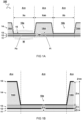
- FIG 1A illustrates a cross-section view of adjacent acoustic transducers 10a, 10b;
- FIG 1B illustrates further details of one of the transducers 10a.
- the acoustic device 100 comprises an array of acoustic transducers 10a, 10b.
- the array is formed by a patterned stack 12-15 on a flexible substrate 11.
- the stack comprises a piezoelectric layer 13 sandwiched between respective bottom and top electrode layers 12,15.
- the stack comprises an insulation layer 14.
- the insulation layer 14 is patterned.
- the patterned insulation layer 14 is formed by a pattern of insulation material 14m.
- the patterned insulation layer (14) comprises insulated areas A14 where the insulation material 14m is disposed between one of the electrodes 12,15 and the piezoelectric layer 13 (in a direction Z transverse to the substrate 11).
- the patterned insulation layer (14) comprises contact areas A10 without the insulation material 14m where both electrodes 12,15 contact the piezoelectric layer 13.
- the acoustic transducers 10a, 10b are formed at the contact areas A10.
- the acoustic transducers 10a, 10b are formed between the insulated areas A14.
- the insulated areas A14 surround and/or separate the respective contact areas A10.
- the pattern of the insulation material 14m may define boundaries around the acoustic transducers 10a, 10b, where the contact areas A10 are formed at gaps in the pattern without any insulation material 14m between the piezoelectric layer 13 and either of the electrodes 12,15.
- an actuation surface of the acoustic transducers 10a, 10b includes part of the flexible substrate 11 at the contact areas A10.
- a respective acoustic transducer 10a can be formed by a stack comprising the flexible substrate 11 with the piezoelectric layer 13 sandwiched between respective bottom and top electrode layers 12,15, but without the insulation material 14m at that area, i.e. the contact areas A10.
- the substrate 11 has relatively high flexibility, e.g. at least sufficient to bend or flex with the piezoelectric layer 13 for generating acoustic waves W, as intended.
- a first flexural rigidity of the substrate 11 can be on the same order as a second flexural rigidity of the stack of layers to be provided on the substrate 11 as part of the transducer (i.e. excluding the insulation material 14m).
- the first flexural rigidity is between a factor 0.1 - 10 times the second flexural rigidity.
- this may be quantified in that the (first) flexural rigidity (of the substrate) constitutes less than ninety percent of the total flexural rigidity Fa of the device at the contact areas A10, i.e. sum of the first and second flexural rigidities.
- the substrate 11 need not be removed and can remain part of the acoustic device 100.
- the stack may be removed from a substrate on which it is manufactured, which may be the flexible substrate or another support substrate.
- the patterned insulation material 14m may provide sufficient structural integrity to support the device without the substrate. This may allow e.g. also the use of a relatively rigid substrate to keep the structure fixed during manufacturing.
- the acoustic device 100 is relatively flat, e.g. formed as a sheet. So, preferably a total thickness Z100 transverse to a plane of the acoustic device 100 is relatively small compared to an extent of its (smallest) in-plane dimension (diameter or length/width).
- the in-plane dimension is more than the thickness by at least a factor ten, twenty, fifty, hundred, thousand, or more.
- the total thickness (Z100) of the substrate 11, the piezoelectric layer 13 with electrodes 12,15, and the insulated areas A14 can be less than a millimeter, less than half a millimeter, e.g. between hundred and two hundred micrometer.
- decoupling can be achieved by providing areas of the substrate separating the transducers with different wave propagation characteristics than the areas forming the transducers.
- dampening can be achieved by providing more and/or different (e.g. dissipative) types of material in the areas between the transducers.
- flexural rigidity F
- v Young's modulus
- Z thickness
- a flexural rigidity Fx at the insulating areas A14 including the insulation layer 14 is higher than a flexural rigidity Fa at the contact areas A10 forming the acoustic transducers 10a,10b by a least a factor ten, more preferably at least a factor twenty, most preferably at least a factor fifty, e.g. a factor between sixty and two hundred.
- the relatively high flexural rigidity of the insulated areas A14 can be provided by using an insulation material 14m with relatively high Young's modulus, e.g. higher than the Young's modulus of the flexible substrate 11.
- a layer thickness Z14 of the insulation material 14m can be relatively high.
- the insulated areas A14 provide a locally increased thickness Z14 to the stack compared to the contact areas A10.
- a thickness Z100 of the stack at the insulated areas A14 (e.g. equal to Z11+Z13+Z14) is higher than a thickness Z10 of the stack at the contact areas A10 (e.g. equal to Z11+Z13) by at least a factor two, preferably at least a factor three.
- the flexural rigidity of the device 100 at the area A10 i.e. the substrate + piezoelectric layer
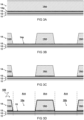
- an additional layer of insulation material 14m was deposited before applying the top electrode 15.
- FIG 2A illustrates a cross-section of an acoustic device 100 wherein the insulation material 14m is applied between the bottom electrode 12 and the piezoelectric layer 13.
- the insulation material 14m is applied between the piezoelectric layer 13 and the top electrode 15.
- the insulation material is formed by a photoresist material. Such material may further improve manufacturability, e.g. providing an easy way to define the pattern of insulation material 14m by a corresponding light pattern / mask to develop the photoresist.
- the patterning of the insulation material 14m can affect the piezoelectric layer 13.
- the photoresist material and/or method of (selectively) removing the photoresist at the contact areas A10 by processes such as wet etching may be alleviated by applying the insulation material 14m before the piezoelectric layer 13.
- FIG 2B illustrates a cross-section of an acoustic device 100 with an intermediate protection layer 14p.
- an intermediate protection layer 14p is disposed between the piezoelectric layer 13 and the insulation material 14m. This may be used alternatively, or additionally, to protect the piezoelectric layer 13 from exposure, e.g. to the insulation material 14m (photoresist) and/or method of removal thereof. In this way, the piezoelectric layer 13 may still be applied before the patterning of the layer of insulation material 14m.
- the protection layer 14p may have a different material than the insulation material 14m. For example, the protection layer 14p may be more resistant to an etching process for removing the insulation material 14m.
- the intermediate protection layer 14p is thereafter locally removed at the contact areas A10. e.g. using another process (than was used for removing the photoresist), such as dry etching (gas).
- the protection layer 14p can act in addition to the insulation material 14m as part of the electrical insulation between the respective electrode and piezoelectric layer and/or as part of the acoustic insulation between neighboring transducers. In that sense, both layers 14m and 14p can be considered part of the patterned insulation material.
- FIGs 3A-3D illustrate a method of manufacturing an acoustic device 100.
- the method comprises providing a stack formed on a flexible substrate 11.
- the stack (initially) comprises at least a bottom electrode 12.
- a layer of insulation material 14m is deposited onto the stack and selectively removed. The places where the insulation material 14m is removed will form the contact areas A10 for electrical contact through the stack with the bottom electrode 12.
- a pre-patterned layer of insulation material e.g. foil with openings, may be applied to the stack (e.g. shown in FIG 7A ).
- the insulation material 14m comprises a photoresist material.
- the patterned insulation layer 14 is formed by a lithographic process.
- the unpatterned layer of insulation material 14m is exposed to a light pattern matching the shape of the contact areas A10 or the shape of the insulated areas A14.
- a mask is used to provide the patterned exposure. It will be appreciated that lithograph can be used to easily form a desired high precision patterns of acoustic transducers, e.g. at relatively small dimensions and/or large numbers.
- a protection layer 14p is provided between the piezoelectric layer 13 and insulation layer 14.
- the protection layer 14p can remain when removing the insulation material 14m to protect the piezoelectric layer 13 against a removal process for patterning the insulation layer 14, e.g. wet etching.
- the protection layer 14p may be removed at the contact areas A10 by a separate process, e.g. dry etching. Accordingly, as shown e.g. in FIG 3D , the top electrode layer 15 can be deposited on the piezoelectric layer 13 without the protection layer 14p there between.
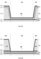
- FIGs 4A and 4B illustrate an acoustic device 100 with the flexible substrate 11 fixed to a support structure 20.
- the flexible substrate 11 is fixed, e.g. laminated, or otherwise disposed on a relatively rigid support substrate 20.
- the substrate 11 can be laminated and/or otherwise adhered to the support substrate 20.
- the fixation between the flexible substrate and the support substrate or other rigid structure may be provided e.g. during and/or after manufacturing.
- the support substrate can be relatively flat similar or thicker compared to the flexible substrate 11.
- the support substrate 20 has a relatively high flexural rigidity compared to the flexible substrate 11, e.g. higher by at least a factor two, three, five, ten, or more. Accordingly, the support substrate 20 may provide additional structural integrity.
- the support substrate 20 is provided with openings 20a-20c at positions corresponding to the acoustic transducers 10a-10c, i.e. at least partially overlapping the contact areas A10.
- the flexible substrate 11 abuts the support structure at the insulated areas A14 while it is not connected to the support structure 20 at the contact areas A10.
- the openings 20a-20c may extend through the support substrate 20, e.g. as shown in FIG 4A .
- the openings 20a-20c may be formed by cavities concavely extending from the direction of the flexible substrate 11 but not completely through the support substrate 20. The openings may allow relatively free movement of the transduced surfaces while still providing a rigid support.
- a support substrate may be provided at the top side, e.g. after depositing completing the stack. Also combinations are possible with support structures on one or both sides, preferably with through openings such as shown in FIG 4A , at least on one side to transmit the acoustic waves W.
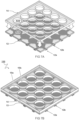
- FIG 5A illustrates a transducer array according to an example layout.
- FIG 5B shows a photograph of a device with similar layout.
- the centers of the transducers may be arranged along a plurality of concentric circles. Accordingly each of the transducers along a respective circle may have the same distance with respect to a point along a central axis of the circles transverse to a plane of the device.
- a first set of transducers along a respective first circle in phase By actuating a first set of transducers along a respective first circle in phase, acoustic waves of those transducers may constructively interfere at points along the central axis.
- a second set of transducers along a respective second circle also in phase within the first set, but with a predetermined phase difference with respect to the first set, an specific point can be selected above a surface of the device at which constructive interference occurs between the sets.
- the device shown can be used to create a haptic feedback device which creates a tangible point in mid-air by the constructive interference between many transducers.
- the location of the point can be controlled by controlling the relative phases between the sets of transducers (along the central axis), or within the respective sets (to move the point off-axis).
- other layouts can be used to create similar or other acoustic devices, e.g. a grid layout.
- a lateral spacing or distance Xab between the neighboring transducers 10a, 10b in any layout can be relatively small, e.g. on the same order as a (maximum or average) diameter Xa,Xb of the transducers 10a,10b.
- the (minimum) distance Xab between the transducers is between 0.1 - 10 times the (constant or average) diameter Xa,Xb of the transducers, preferably between 0.2 - 5 times, more preferably, between half and two times.
- a density of the transducers over the surface of the device can be relatively high, e.g.
- the transducers may cover at least ten percent of the surface (the remaining surface formed by the areas between the transducers), preferably at least twenty percent, more preferably at least thirty percent, or even more than fifty percent. The more of the surface can be covered by the transducers, the more effective can the device operate.
- FIG 6 illustrates a measurement of a deflection ⁇ Z (in nanometers) over a surface X,Y of an acoustic device, such as shown in FIG 5B , where the transducers are actuated.
- the measurement was performed using a laser vibrometer.
- the deflection ⁇ Z is limited to the contact areas of the transducers, while there is virtually no noticeable deflection at the insulated areas between the transducers, e.g. the deflection at the insulated areas is at least a factor ten less than the deflection at the contact areas.
- FIGs 7A and 7B illustrate another layout of acoustic transducers 10a,10b.
- the insulation layer 14 is pre-patterned before being applied to the stack.
- the insulation layer 14 shown in FIG 7B may be patterned by selective removal of material as was described e.g. with reference to FIGs 3A-3D .
- the piezoelectric layer 13 is a continuous layer extending between different transducers 10a, 10b.
- a polymer based piezoelectric material is used for the piezoelectric layer 13.
- polymer based piezoelectric material can be easily applied as a continuous layer.
- the deposited piezoelectric material may initially have domains that are randomly oriented. Preferably, these are aligned by "poling" the piezoelectric material, i.e. a process by which a strong electric field is applied across the material, usually at elevated temperatures.
- the piezoelectric layer 13 is exclusively (or predominantly) poled at the contact areas A10.
- the strong electric field for poling is applied via the bottom electrode 12 and top electrode (not visible here). Due to the patterned insulation layer 14, a voltage difference between the electrodes may result in an electric field which is stronger across the piezoelectric layer 13 at the contact areas A10 than across the larger gap of the insulated areas A14.
- the selective poling may also help to improve functionality, e.g. further prevent actuation of the piezoelectric layer 13 at the non-poled regions of the insulated areas A14.
- At least one of the bottom and top electrodes is a continuous layer extending between different transducers 10a, 10b.
- at least one of the electrodes 12,15 is patterned.
- a combination of a patterned and unpatterned electrode layer is used.
- the patterning of the electrodes is such that subsets of one or more of the acoustic transducers 10a, 10b can be selectively actuated.
- a first set of one or more transducers 10a is actuated by applying a voltage to a first line 12a of the bottom electrode
- a different, second set of one or more transducers 10b is actuated by applying a voltage to a different, second line 12a of the bottom electrode.
- the lines 12a,12b may comprise contact pads shaped to cover at least the contact areas A10.
- the top electrode may be patterned (not shown).
- the pattern of the top electrode may complement the pattern of the bottom electrode, e.g. forming perpendicular grid lines.
- a grid of electrode lines may be formed on one side of the piezoelectric layer 13.
- the grid may comprise thin film transistors (TFT).
Landscapes
- Engineering & Computer Science (AREA)
- Mechanical Engineering (AREA)
- Transducers For Ultrasonic Waves (AREA)
- Ultra Sonic Daignosis Equipment (AREA)
- Apparatuses For Generation Of Mechanical Vibrations (AREA)
Claims (15)
- Akustische Vorrichtung (100) mit einer Anordnung von Schallwandlern (10a, 10b), die durch einen strukturierten Stapel (12-15) auf einem flexiblen Substrat (11) ausgebildet ist, wobei der Stapel aufweist:- eine piezoelektrische Schicht (13), die zwischen eine untere und eine obere Elektrodenschicht (12, 15) geschichtet ist; und- eine strukturierte Isolationsschicht (14), die durch eine Struktur aus Isolationsmaterial (14m) ausgebildet ist, wobei die Struktur aufweist:dadurch gekennzeichnet, dass die piezoelektrische Schicht (13) eine durchgängige piezoelektrische Schicht ist, die zwischen unterschiedlichen Wandlern (10a, 10b) verläuft.∘ isolierte Bereiche (A14), in denen das Isolationsmaterial (14m) zwischen einer der Elektroden (12, 15) und der piezoelektrischen Schicht (13) angeordnet ist, und∘ Kontaktbereiche (A10) ohne das Isolationsmaterial (14m), in denen beide Elektroden (12, 15) die piezoelektrische Schicht (13) kontaktieren,
- Akustische Vorrichtung nach Anspruch 1, wobei eine Betätigungsfläche der Schallwandler (10a, 10b) einen Abschnitt des flexiblen Substrats (11) bei den Kontaktbereichen (A10) umfasst.
- Akustische Vorrichtung nach einem der vorhergehenden Ansprüche, wobei eine Gesamtdicke (Z100) des flexiblen Substrats (11), der piezoelektrischen Schicht (13) mit den Elektroden (12, 15) und der isolierten Bereiche (A14) weniger als ein Millimeter ist.
- Akustische Vorrichtung nach einem der vorhergehenden Ansprüche, wobei eine Dicke (Z100) des Stapels bei den isolierten Bereichen (A14) um mindestens einen Faktor zwei höher als eine Dicke (Z10) des Stapels bei den Kontaktbereichen (A10) ist.
- Akustische Vorrichtung nach einem der vorhergehenden Ansprüche, wobei eine Biegesteifigkeit (Fx) bei den isolierenden Bereichen (A14) einschließlich der Isolationsschicht (14) um mindestens einen Faktor zehn höher ist als eine Biegesteifigkeit (Fa) bei den Kontaktbereichen (A10), welche die Schallwandler (10a, 10b) ausbilden.
- Akustische Vorrichtung nach einem der vorhergehenden Ansprüche, wobei das Isolationsmaterial (14m) zwischen der piezoelektrischen Schicht (13) und der oberen Elektrodenschicht (15) angeordnet ist.
- Akustische Vorrichtung nach einem der vorhergehenden Ansprüche, wobei das Isolationsmaterial (14m) ein Photoresistmaterial umfasst.
- Akustische Vorrichtung nach einem der vorhergehenden Ansprüche, wobei zwischen der piezoelektrischen Schicht (13) und dem Isolationsmaterial (14m) eine zwischengelagerte Schutzschicht (14p) angeordnet ist, wobei die Schutzschicht (14p) gegen einen Ätzprozess zum Entfernen des Isolationsmaterials (14m) resistent ist.
- Akustische Vorrichtung nach einem der vorhergehenden Ansprüche, wobei ein Abstand (Xab) zwischen nächstbenachbarten Wandlern (10a, 10b) zwischen der Hälfte und dem Doppelten eines Durchmessers (Xa, Xb) der nächstbenachbarten Wandler (10a, 10b) beträgt.
- Akustische Vorrichtung nach einem der vorhergehenden Ansprüche, wobei die piezoelektrische Schicht (13) ausschließlich in den Kontaktbereichen (A10) gepolt ist.
- Akustische Vorrichtung nach einem der vorhergehenden Ansprüche, wobei eine der Elektroden (15) eine durchgängige Schicht ist, die zwischen verschiedenen Wandlern (10a, 10b) verläuft, und die andere der Elektroden (12) zum steuerbaren Betätigen unterschiedlicher Teilmengen der Wandler (10a, 10b) strukturiert ist.
- Akustische Vorrichtung nach einem der vorhergehenden Ansprüche, wobei die akustische Vorrichtung (100) eine Vorrichtung mit haptischem Feedback ausbildet, wobei die Wandler entlang mehreren konzentrischen Kreisen angeordnet sind, die dazu eingerichtet sind, durch konstruktive Interferenz zwischen von den Wandlern unterschiedlicher der konzentrischen Kreise emittierten Schallwellen (W) einen berührbaren Punkt in der Luft oberhalb der Vorrichtung entlang einer Mittellinie der konzentrischen Kreise zu erzeugen.
- Akustische Vorrichtung nach einem der vorhergehenden Ansprüche, wobei das flexible Substrat (11) auf einem starren Trägersubstrat (20) fixiert ist, wobei eine Biegesteifigkeit des starren Trägersubstrats (20) um mindestens einen Faktor zwei höher als eine Biegesteifigkeit des flexiblen Substrats (11) ist.
- Akustische Vorrichtung nach Anspruch 13, wobei das Trägersubstrat (20) mit Öffnungen (20a-20c) an den Schallwandlern (10a-10c) entsprechenden Positionen versehen ist.
- Verfahren zum Herstellen einer akustischen Vorrichtung (100), wobei das Verfahren umfasst:- Bereitstellen eines Stapels, der auf einem flexiblen Substrat (11) ausgebildet ist, wobei der Stapel mindestens eine untere Elektrode (12) aufweist;- Aufbringen einer Schicht aus Isolationsmaterial (14m) auf den Stapel und selektives Entfernen des Isolationsmaterials (14m), um Kontaktbereiche (A10) für elektrischen Kontakt durch den Stapel mit der unteren Elektrode (12) auszubilden; und- Aufbringen einer oberen Elektrode (15) auf den Stapel, um in den Kontaktbereichen (A10), in denen die obere und die untere Elektrode eine zwischen ihnen angeordnete piezoelektrische Schicht (13) kontaktieren, eine Anordnung von Schallwandlern (10a, 10b) auszubilden, wobei die piezoelektrische Schicht (13) vor oder nach dem Aufbringen der Schicht aus Isolationsmaterial (14m) auf den Stapel aufgebracht wird, wobei die Schallwandler (10a, 10b) durch isolierte Bereiche (A14) voneinander getrennt sind, in welchen das Isolationsmaterial (14m) zwischen einer der Elektroden (12, 15) und der piezoelektrischen Schicht (13) angeordnet ist, dadurch gekennzeichnet, dass die piezoelektrische Schicht (13) eine durchgängige Schicht ist, die zwischen unterschiedlichen Wandlern (10a, 10b) verläuft.
Applications Claiming Priority (2)
| Application Number | Priority Date | Filing Date | Title |
|---|---|---|---|
| EP19171943.4A EP3733310A1 (de) | 2019-04-30 | 2019-04-30 | Akustische piezoelektrische membranwandler-arrays mit lokalisierten membranschwingungen |
| PCT/NL2020/050265 WO2020222639A1 (en) | 2019-04-30 | 2020-04-29 | Acoustic piezoelectric membrane transducer arrays with localized membrane vibrations |
Publications (3)
| Publication Number | Publication Date |
|---|---|
| EP3962665A1 EP3962665A1 (de) | 2022-03-09 |
| EP3962665B1 true EP3962665B1 (de) | 2024-10-09 |
| EP3962665C0 EP3962665C0 (de) | 2024-10-09 |
Family
ID=66349354
Family Applications (2)
| Application Number | Title | Priority Date | Filing Date |
|---|---|---|---|
| EP19171943.4A Withdrawn EP3733310A1 (de) | 2019-04-30 | 2019-04-30 | Akustische piezoelektrische membranwandler-arrays mit lokalisierten membranschwingungen |
| EP20723223.2A Active EP3962665B1 (de) | 2019-04-30 | 2020-04-29 | Akustische piezoelektrische membranwandler-arrays mit lokalisierten membranschwingungen |
Family Applications Before (1)
| Application Number | Title | Priority Date | Filing Date |
|---|---|---|---|
| EP19171943.4A Withdrawn EP3733310A1 (de) | 2019-04-30 | 2019-04-30 | Akustische piezoelektrische membranwandler-arrays mit lokalisierten membranschwingungen |
Country Status (5)
| Country | Link |
|---|---|
| US (1) | US20220193723A1 (de) |
| EP (2) | EP3733310A1 (de) |
| JP (1) | JP7641237B2 (de) |
| CN (1) | CN113766977A (de) |
| WO (1) | WO2020222639A1 (de) |
Families Citing this family (6)
| Publication number | Priority date | Publication date | Assignee | Title |
|---|---|---|---|---|
| FR3116630B1 (fr) * | 2020-11-26 | 2023-06-02 | Commissariat A L’Energie Atomique Et Aux Energies Alternatives | Interface haptique |
| EP4016074A1 (de) * | 2020-12-18 | 2022-06-22 | Universite De Franche-Comte | Testanordnung mit akustischem biosensor |
| WO2022141585A1 (zh) * | 2020-12-31 | 2022-07-07 | 深圳市韶音科技有限公司 | 一种骨传导传声装置 |
| US11843915B2 (en) * | 2021-08-20 | 2023-12-12 | Massachusetts Institute Of Technology | Active piezoelectric sheet with piezoelectric microstructures |
| CN115148893B (zh) * | 2022-07-28 | 2025-09-19 | 西安交通大学 | 一种具有弯曲和扭转变形功能的柔性PMUTs及其制备方法 |
| CN117750285B (zh) * | 2024-02-07 | 2024-05-07 | 山东博华电子科技发展有限公司 | 微型压电换能器的制备方法及微型压电换能器 |
Family Cites Families (20)
| Publication number | Priority date | Publication date | Assignee | Title |
|---|---|---|---|---|
| JPS555570A (en) * | 1978-06-28 | 1980-01-16 | Furuno Electric Co Ltd | Ultrasonic wave reception unit |
| GB9108490D0 (en) * | 1991-04-20 | 1991-06-05 | Jones Richard W | Device for acoustic wave generation |
| EP1769759B1 (de) * | 1999-05-11 | 2008-08-13 | Atrionix, Inc. | Vorrichtung zur Ultraschallablation |
| JP2002027594A (ja) * | 2000-07-11 | 2002-01-25 | Hitachi Ltd | 超音波探触子およびその製造方法 |
| JP2006333121A (ja) * | 2005-05-26 | 2006-12-07 | Mitsubishi Electric Engineering Co Ltd | 超指向性スピーカ |
| JP2008072482A (ja) * | 2006-09-14 | 2008-03-27 | Mitsubishi Electric Engineering Co Ltd | スピーカ装置 |
| JP4600468B2 (ja) * | 2007-12-10 | 2010-12-15 | セイコーエプソン株式会社 | 半導体圧力センサ及びその製造方法、半導体装置並びに電子機器 |
| DE102008029378B4 (de) * | 2008-06-20 | 2010-04-15 | Siemens Aktiengesellschaft | Anordnung eines piezoakustischen Resonators auf einem akustischen Spiegel eines Substrats, Verfahren zum Herstellen der Anordnung und Verwendung der Anordnung |
| WO2010033867A1 (en) * | 2008-09-18 | 2010-03-25 | Visualsonics Inc. | Methods for acquisition and display in ultrasound imaging |
| US9173047B2 (en) * | 2008-09-18 | 2015-10-27 | Fujifilm Sonosite, Inc. | Methods for manufacturing ultrasound transducers and other components |
| CN101712028B (zh) * | 2009-11-13 | 2012-02-01 | 中国科学院声学研究所 | 一种薄膜超声换能器及其制备方法 |
| WO2012107388A1 (de) * | 2011-02-07 | 2012-08-16 | Deutsches Zentrum für Luft- und Raumfahrt e.V. | Transparente akustisch wirksame vorrichtung |
| US9061320B2 (en) | 2012-05-01 | 2015-06-23 | Fujifilm Dimatix, Inc. | Ultra wide bandwidth piezoelectric transducer arrays |
| US8969170B2 (en) * | 2013-03-14 | 2015-03-03 | Globalfoundries Inc. | Method of forming a semiconductor structure including a metal-insulator-metal capacitor |
| CN103240220B (zh) * | 2013-05-09 | 2015-06-17 | 电子科技大学 | 一种压电式阵列超声换能器 |
| US9604255B2 (en) * | 2014-01-10 | 2017-03-28 | Fujifilm Dimatix, Inc. | Method, apparatus and system for a transferable micromachined piezoelectric transducer array |
| JP6606866B2 (ja) * | 2015-05-29 | 2019-11-20 | セイコーエプソン株式会社 | 圧電デバイスおよびプローブ並びに電子機器および超音波画像装置 |
| EP3703874B1 (de) * | 2017-10-31 | 2022-05-18 | Koninklijke Philips N.V. | Ultraschall-scanneranordnung |
| WO2020131020A1 (en) * | 2018-12-17 | 2020-06-25 | Emerge Now Inc. | Systems for interfacing with immersive computing environments |
| US11950512B2 (en) * | 2020-03-23 | 2024-04-02 | Apple Inc. | Thin-film acoustic imaging system for imaging through an exterior surface of an electronic device housing |
-
2019
- 2019-04-30 EP EP19171943.4A patent/EP3733310A1/de not_active Withdrawn
-
2020
- 2020-04-29 CN CN202080032588.2A patent/CN113766977A/zh active Pending
- 2020-04-29 EP EP20723223.2A patent/EP3962665B1/de active Active
- 2020-04-29 WO PCT/NL2020/050265 patent/WO2020222639A1/en not_active Ceased
- 2020-04-29 JP JP2021564578A patent/JP7641237B2/ja active Active
- 2020-04-29 US US17/605,437 patent/US20220193723A1/en active Pending
Also Published As
| Publication number | Publication date |
|---|---|
| EP3733310A1 (de) | 2020-11-04 |
| US20220193723A1 (en) | 2022-06-23 |
| CN113766977A (zh) | 2021-12-07 |
| EP3962665A1 (de) | 2022-03-09 |
| EP3962665C0 (de) | 2024-10-09 |
| JP2022530663A (ja) | 2022-06-30 |
| JP7641237B2 (ja) | 2025-03-06 |
| WO2020222639A1 (en) | 2020-11-05 |
Similar Documents
| Publication | Publication Date | Title |
|---|---|---|
| EP3962665B1 (de) | Akustische piezoelektrische membranwandler-arrays mit lokalisierten membranschwingungen | |
| EP1511092B1 (de) | Laminierte Struktur, Verfahren zur Herstellung derselben und Vielfach-Ultraschallwandlerfeld | |
| JP6251661B2 (ja) | 超音波トランスデューサ、その製造方法、超音波トランスデューサアレイ及び超音波検査装置 | |
| JP7376008B2 (ja) | 高周波超音波トランスデューサ | |
| US6168906B1 (en) | Micromachined membrane with locally compliant and stiff regions and method of making same | |
| US10081533B2 (en) | Micromechanical structure and method for fabricating the same | |
| KR20180031744A (ko) | Dsr 스피커 요소 및 그 제조 방법 | |
| EP3869575A1 (de) | Piezoelektrische vorrichtung mit säulenstruktur und herstellungsverfahren | |
| JP7215802B2 (ja) | 微細機械加工素子のアレイを含むデバイスを設計及び製造するためのプロセス、そのようなプロセスの最後に得られるデバイス | |
| JP7576084B2 (ja) | 音響膜アレイの最適化 | |
| JP2009198493A (ja) | 角速度検出装置 | |
| EP4017651B1 (de) | Verfahren zur herstellung eines ultraschallwandlers | |
| JP7768043B2 (ja) | Memsトランスデューサ | |
| EP4335558A1 (de) | Akustische vorrichtung und verfahren zur herstellung | |
| IT202200024411A1 (it) | Dispositivo trasduttore mems per applicazioni ad alta frequenza, e metodo di fabbricazione | |
| JP2025073733A (ja) | 電気音響変換器 | |
| KR20230135534A (ko) | 소리 생성 셀, 음향 변환기 및 소리 생성 셀의 제조 방법 | |
| Zhang et al. | CMUTs with interlaced high-and low-frequency elements | |
| JP2005102181A (ja) | 積層構造体及びその製造方法、並びに、超音波トランスデューサアレイ |
Legal Events
| Date | Code | Title | Description |
|---|---|---|---|
| STAA | Information on the status of an ep patent application or granted ep patent |
Free format text: STATUS: UNKNOWN |
|
| STAA | Information on the status of an ep patent application or granted ep patent |
Free format text: STATUS: THE INTERNATIONAL PUBLICATION HAS BEEN MADE |
|
| PUAI | Public reference made under article 153(3) epc to a published international application that has entered the european phase |
Free format text: ORIGINAL CODE: 0009012 |
|
| STAA | Information on the status of an ep patent application or granted ep patent |
Free format text: STATUS: REQUEST FOR EXAMINATION WAS MADE |
|
| 17P | Request for examination filed |
Effective date: 20211102 |
|
| AK | Designated contracting states |
Kind code of ref document: A1 Designated state(s): AL AT BE BG CH CY CZ DE DK EE ES FI FR GB GR HR HU IE IS IT LI LT LU LV MC MK MT NL NO PL PT RO RS SE SI SK SM TR |
|
| DAV | Request for validation of the european patent (deleted) | ||
| DAX | Request for extension of the european patent (deleted) | ||
| P01 | Opt-out of the competence of the unified patent court (upc) registered |
Effective date: 20230522 |
|
| GRAP | Despatch of communication of intention to grant a patent |
Free format text: ORIGINAL CODE: EPIDOSNIGR1 |
|
| STAA | Information on the status of an ep patent application or granted ep patent |
Free format text: STATUS: GRANT OF PATENT IS INTENDED |
|
| INTG | Intention to grant announced |
Effective date: 20240429 |
|
| GRAS | Grant fee paid |
Free format text: ORIGINAL CODE: EPIDOSNIGR3 |
|
| GRAA | (expected) grant |
Free format text: ORIGINAL CODE: 0009210 |
|
| STAA | Information on the status of an ep patent application or granted ep patent |
Free format text: STATUS: THE PATENT HAS BEEN GRANTED |
|
| AK | Designated contracting states |
Kind code of ref document: B1 Designated state(s): AL AT BE BG CH CY CZ DE DK EE ES FI FR GB GR HR HU IE IS IT LI LT LU LV MC MK MT NL NO PL PT RO RS SE SI SK SM TR |
|
| REG | Reference to a national code |
Ref country code: CH Ref legal event code: EP |
|
| REG | Reference to a national code |
Ref country code: DE Ref legal event code: R096 Ref document number: 602020039035 Country of ref document: DE |
|
| REG | Reference to a national code |
Ref country code: IE Ref legal event code: FG4D |
|
| U01 | Request for unitary effect filed |
Effective date: 20241029 |
|
| U07 | Unitary effect registered |
Designated state(s): AT BE BG DE DK EE FI FR IT LT LU LV MT NL PT RO SE SI Effective date: 20241111 |
|
| PG25 | Lapsed in a contracting state [announced via postgrant information from national office to epo] |
Ref country code: IS Free format text: LAPSE BECAUSE OF FAILURE TO SUBMIT A TRANSLATION OF THE DESCRIPTION OR TO PAY THE FEE WITHIN THE PRESCRIBED TIME-LIMIT Effective date: 20250209 Ref country code: HR Free format text: LAPSE BECAUSE OF FAILURE TO SUBMIT A TRANSLATION OF THE DESCRIPTION OR TO PAY THE FEE WITHIN THE PRESCRIBED TIME-LIMIT Effective date: 20241009 |
|
| PG25 | Lapsed in a contracting state [announced via postgrant information from national office to epo] |
Ref country code: ES Free format text: LAPSE BECAUSE OF FAILURE TO SUBMIT A TRANSLATION OF THE DESCRIPTION OR TO PAY THE FEE WITHIN THE PRESCRIBED TIME-LIMIT Effective date: 20241009 |
|
| PG25 | Lapsed in a contracting state [announced via postgrant information from national office to epo] |
Ref country code: NO Free format text: LAPSE BECAUSE OF FAILURE TO SUBMIT A TRANSLATION OF THE DESCRIPTION OR TO PAY THE FEE WITHIN THE PRESCRIBED TIME-LIMIT Effective date: 20250109 |
|
| PG25 | Lapsed in a contracting state [announced via postgrant information from national office to epo] |
Ref country code: GR Free format text: LAPSE BECAUSE OF FAILURE TO SUBMIT A TRANSLATION OF THE DESCRIPTION OR TO PAY THE FEE WITHIN THE PRESCRIBED TIME-LIMIT Effective date: 20250110 |
|
| PG25 | Lapsed in a contracting state [announced via postgrant information from national office to epo] |
Ref country code: PL Free format text: LAPSE BECAUSE OF FAILURE TO SUBMIT A TRANSLATION OF THE DESCRIPTION OR TO PAY THE FEE WITHIN THE PRESCRIBED TIME-LIMIT Effective date: 20241009 |
|
| PG25 | Lapsed in a contracting state [announced via postgrant information from national office to epo] |
Ref country code: RS Free format text: LAPSE BECAUSE OF FAILURE TO SUBMIT A TRANSLATION OF THE DESCRIPTION OR TO PAY THE FEE WITHIN THE PRESCRIBED TIME-LIMIT Effective date: 20250109 |
|
| U20 | Renewal fee for the european patent with unitary effect paid |
Year of fee payment: 6 Effective date: 20250425 |
|
| PG25 | Lapsed in a contracting state [announced via postgrant information from national office to epo] |
Ref country code: SM Free format text: LAPSE BECAUSE OF FAILURE TO SUBMIT A TRANSLATION OF THE DESCRIPTION OR TO PAY THE FEE WITHIN THE PRESCRIBED TIME-LIMIT Effective date: 20241009 |
|
| PGFP | Annual fee paid to national office [announced via postgrant information from national office to epo] |
Ref country code: GB Payment date: 20250423 Year of fee payment: 6 |
|
| PG25 | Lapsed in a contracting state [announced via postgrant information from national office to epo] |
Ref country code: SK Free format text: LAPSE BECAUSE OF FAILURE TO SUBMIT A TRANSLATION OF THE DESCRIPTION OR TO PAY THE FEE WITHIN THE PRESCRIBED TIME-LIMIT Effective date: 20241009 |
|
| PG25 | Lapsed in a contracting state [announced via postgrant information from national office to epo] |
Ref country code: CZ Free format text: LAPSE BECAUSE OF FAILURE TO SUBMIT A TRANSLATION OF THE DESCRIPTION OR TO PAY THE FEE WITHIN THE PRESCRIBED TIME-LIMIT Effective date: 20241009 |
|
| PLBE | No opposition filed within time limit |
Free format text: ORIGINAL CODE: 0009261 |
|
| STAA | Information on the status of an ep patent application or granted ep patent |
Free format text: STATUS: NO OPPOSITION FILED WITHIN TIME LIMIT |
|
| 26N | No opposition filed |
Effective date: 20250710 |
|
| REG | Reference to a national code |
Ref country code: CH Ref legal event code: H13 Free format text: ST27 STATUS EVENT CODE: U-0-0-H10-H13 (AS PROVIDED BY THE NATIONAL OFFICE) Effective date: 20251125 |
|
| PG25 | Lapsed in a contracting state [announced via postgrant information from national office to epo] |
Ref country code: MC Free format text: LAPSE BECAUSE OF FAILURE TO SUBMIT A TRANSLATION OF THE DESCRIPTION OR TO PAY THE FEE WITHIN THE PRESCRIBED TIME-LIMIT Effective date: 20241009 |