EP3961998A1 - Automatische vorrichtungsordnung - Google Patents
Automatische vorrichtungsordnung Download PDFInfo
- Publication number
- EP3961998A1 EP3961998A1 EP21185483.1A EP21185483A EP3961998A1 EP 3961998 A1 EP3961998 A1 EP 3961998A1 EP 21185483 A EP21185483 A EP 21185483A EP 3961998 A1 EP3961998 A1 EP 3961998A1
- Authority
- EP
- European Patent Office
- Prior art keywords
- node
- node device
- pulse
- order
- data lines
- Prior art date
- Legal status (The legal status is an assumption and is not a legal conclusion. Google has not performed a legal analysis and makes no representation as to the accuracy of the status listed.)
- Withdrawn
Links
Images






Classifications
-
- H—ELECTRICITY
- H04—ELECTRIC COMMUNICATION TECHNIQUE
- H04L—TRANSMISSION OF DIGITAL INFORMATION, e.g. TELEGRAPHIC COMMUNICATION
- H04L61/00—Network arrangements, protocols or services for addressing or naming
- H04L61/50—Address allocation
- H04L61/5038—Address allocation for local use, e.g. in LAN or USB networks, or in a controller area network [CAN]
-
- G—PHYSICS
- G01—MEASURING; TESTING
- G01S—RADIO DIRECTION-FINDING; RADIO NAVIGATION; DETERMINING DISTANCE OR VELOCITY BY USE OF RADIO WAVES; LOCATING OR PRESENCE-DETECTING BY USE OF THE REFLECTION OR RERADIATION OF RADIO WAVES; ANALOGOUS ARRANGEMENTS USING OTHER WAVES
- G01S13/00—Systems using the reflection or reradiation of radio waves, e.g. radar systems; Analogous systems using reflection or reradiation of waves whose nature or wavelength is irrelevant or unspecified
- G01S13/02—Systems using reflection of radio waves, e.g. primary radar systems; Analogous systems
- G01S13/06—Systems determining position data of a target
- G01S13/08—Systems for measuring distance only
- G01S13/10—Systems for measuring distance only using transmission of interrupted, pulse modulated waves
- G01S13/12—Systems for measuring distance only using transmission of interrupted, pulse modulated waves wherein the pulse-recurrence frequency is varied to provide a desired time relationship between the transmission of a pulse and the receipt of the echo of a preceding pulse
-
- G—PHYSICS
- G01—MEASURING; TESTING
- G01S—RADIO DIRECTION-FINDING; RADIO NAVIGATION; DETERMINING DISTANCE OR VELOCITY BY USE OF RADIO WAVES; LOCATING OR PRESENCE-DETECTING BY USE OF THE REFLECTION OR RERADIATION OF RADIO WAVES; ANALOGOUS ARRANGEMENTS USING OTHER WAVES
- G01S13/00—Systems using the reflection or reradiation of radio waves, e.g. radar systems; Analogous systems using reflection or reradiation of waves whose nature or wavelength is irrelevant or unspecified
- G01S13/02—Systems using reflection of radio waves, e.g. primary radar systems; Analogous systems
- G01S13/06—Systems determining position data of a target
- G01S13/08—Systems for measuring distance only
- G01S13/10—Systems for measuring distance only using transmission of interrupted, pulse modulated waves
- G01S13/26—Systems for measuring distance only using transmission of interrupted, pulse modulated waves wherein the transmitted pulses use a frequency- or phase-modulated carrier wave
- G01S13/28—Systems for measuring distance only using transmission of interrupted, pulse modulated waves wherein the transmitted pulses use a frequency- or phase-modulated carrier wave with time compression of received pulses
-
- H—ELECTRICITY
- H04—ELECTRIC COMMUNICATION TECHNIQUE
- H04L—TRANSMISSION OF DIGITAL INFORMATION, e.g. TELEGRAPHIC COMMUNICATION
- H04L12/00—Data switching networks
- H04L12/28—Data switching networks characterised by path configuration, e.g. LAN [Local Area Networks] or WAN [Wide Area Networks]
- H04L12/40—Bus networks
- H04L12/40052—High-speed IEEE 1394 serial bus
- H04L12/40097—Interconnection with other networks
-
- H—ELECTRICITY
- H04—ELECTRIC COMMUNICATION TECHNIQUE
- H04L—TRANSMISSION OF DIGITAL INFORMATION, e.g. TELEGRAPHIC COMMUNICATION
- H04L12/00—Data switching networks
- H04L12/28—Data switching networks characterised by path configuration, e.g. LAN [Local Area Networks] or WAN [Wide Area Networks]
- H04L12/40—Bus networks
- H04L12/40052—High-speed IEEE 1394 serial bus
- H04L12/40123—Interconnection of computers and peripherals
-
- H—ELECTRICITY
- H04—ELECTRIC COMMUNICATION TECHNIQUE
- H04L—TRANSMISSION OF DIGITAL INFORMATION, e.g. TELEGRAPHIC COMMUNICATION
- H04L2101/00—Indexing scheme associated with group H04L61/00
- H04L2101/60—Types of network addresses
- H04L2101/618—Details of network addresses
- H04L2101/622—Layer-2 addresses, e.g. medium access control [MAC] addresses
Definitions
- the subject matter disclosed herein relates to automatic device ordering.
- the apparatus includes a processor and a memory storing code executable by the processor.
- the processor configures each node device on a serial network for an order measurement.
- the processor further measures an order parameter for each of the node devices.
- the processor determines an order number of each of the node devices based on the order parameter for the node device.
- a method for automatic device ordering is also disclosed.
- the method configures, by use of a processor, each node device on a serial network for an order measurement.
- the method measures an order parameter for each of the node devices.
- the method determines an order number of each of the node devices based on the order parameter for the node device.
- a computer program product for automatic device ordering comprises a non-transitory computer readable storage medium having code embodied therein.
- the code is readable/executable by a processor.
- the processor configures each node device on a serial network for an order measurement.
- the processor further measures an order parameter for each of the node devices.
- the processor determines an order number of each of the node devices based on the order parameter for the node device.
- aspects of the present invention may be embodied as a system, method, and/or computer program product. Accordingly, aspects of the present invention may take the form of an entirely hardware embodiment, an entirely software embodiment (including firmware, resident software, micro-code, etc.) or an embodiment combining software and hardware aspects that may all generally be referred to herein as a "circuit,” "module,” or “system.” Furthermore, aspects of the present invention may take the form of a computer program product embodied in one or more computer readable medium(s) having program code embodied thereon.
- modules may be implemented as a hardware circuit comprising custom VLSI circuits or gate arrays, off-the-shelf semiconductors such as logic chips, transistors, or other discrete components.
- a module may also be implemented in programmable hardware devices such as field programmable gate arrays, programmable array logic, programmable logic devices or the like.
- Modules may also be implemented in software for execution by various types of processors.
- An identified module of program code may, for instance, comprise one or more physical or logical blocks of computer instructions which may, for instance, be organized as an object, procedure, or function. Nevertheless, the executables of an identified module need not be physically located together but may comprise disparate instructions stored in different locations which, when joined logically together, comprise the module and achieve the stated purpose for the module.
- a module of program code may be a single instruction, or many instructions, and may even be distributed over several different code segments, among different programs, and across several memory devices.
- operational data may be identified and illustrated herein within modules and may be embodied in any suitable form and organized within any suitable type of data structure. The operational data may be collected as a single data set or may be distributed over different locations including over different storage devices, and may exist, at least partially, merely as electronic signals on a system or network.
- the program code may be stored and/or propagated on in one or more computer readable medium(s).
- the computer readable medium may be a tangible computer readable storage medium storing the program code.
- the computer readable storage medium may be, for example, but not limited to, an electronic, magnetic, optical, electromagnetic, infrared, holographic, micromechanical, or semiconductor system, apparatus, or device, or any suitable combination of the foregoing.
- the computer readable storage medium may include but are not limited to a portable computer diskette, a hard disk, a random access memory (RAM), a read-only memory (ROM), an erasable programmable read-only memory (EPROM or Flash memory), a portable compact disc read-only memory (CD-ROM), a digital versatile disc (DVD), an optical storage device, a magnetic storage device, a holographic storage medium, a micromechanical storage device, or any suitable combination of the foregoing.
- a computer readable storage medium may be any tangible medium that can contain, and/or store program code for use by and/or in connection with an instruction execution system, apparatus, or device.
- the computer readable medium may also be a computer readable signal medium.
- a computer readable signal medium may include a propagated data signal with program code embodied therein, for example, in baseband or as part of a carrier wave. Such a propagated signal may take any of a variety of forms, including, but not limited to, electrical, electro-magnetic, magnetic, optical, or any suitable combination thereof
- a computer readable signal medium may be any computer readable medium that is not a computer readable storage medium and that can communicate, propagate, or transport program code for use by or in connection with an instruction execution system, apparatus, or device.
- Program code embodied on a computer readable signal medium may be transmitted using any appropriate medium, including but not limited to wireline, optical fiber, Radio Frequency (RF), or the like, or any suitable combination of the foregoing
- the computer readable medium may comprise a combination of one or more computer readable storage mediums and one or more computer readable signal mediums.
- program code may be both propagated as an electro-magnetic signal through a fiber optic cable for execution by a processor and stored on RAM storage device for execution by the processor.
- Program code for carrying out operations for aspects of the present invention may be written in any combination of one or more programming languages, including an object oriented programming language such as Python, Ruby, R, Java, Java Script, Smalltalk, C++, C sharp, Lisp, Clojure, PHP or the like and conventional procedural programming languages, such as the "C" programming language or similar programming languages.
- the program code may execute entirely on the user's computer, partly on the user's computer, as a stand-alone software package, partly on the user's computer and partly on a remote computer or entirely on the remote computer or server.
- the remote computer may be connected to the user's computer through any type of network, including a local area network (LAN) or a wide area network (WAN), or the connection may be made to an external computer (for example, through the Internet using an Internet Service Provider).
- LAN local area network
- WAN wide area network
- the computer program product may be shared, simultaneously serving multiple customers in a flexible, automated fashion.
- the computer program product may be integrated into a client, server and network environment by providing for the computer program product to coexist with applications, operating systems and network operating systems software and then installing the computer program product on the clients and servers in the environment where the computer program product will function.
- software is identified on the clients and servers including the network operating system where the computer program product will be deployed that are required by the computer program product or that work in conjunction with the computer program product. This includes the network operating system that is software that enhances a basic operating system by adding networking features.
- the embodiments may transmit data between electronic devices.
- the embodiments may further convert the data from a first format to a second format, including converting the data from a non-standard format to a standard format and/or converting the data from the standard format to a non-standard format.
- the embodiments may modify, update, and/or process the data.
- the embodiments may store the received, converted, modified, updated, and/or processed data.
- the embodiments may provide remote access to the data including the updated data.
- the embodiments may make the data and/or updated data available in real time.
- the embodiments may generate and transmit a message based on the data and/or updated data in real time.
- the program code may also be stored in a computer readable medium that can direct a computer, other programmable data processing apparatus, or other devices to function in a particular manner, such that the instructions stored in the computer readable medium produce an article of manufacture including instructions which implement the function/act specified in the schematic flowchart diagrams and/or schematic block diagrams block or blocks.
- the program code may also be loaded onto a computer, other programmable data processing apparatus, or other devices to cause a series of operational steps to be performed on the computer, other programmable apparatus or other devices to produce a computer implemented process such that the program code which executed on the computer or other programmable apparatus provide processes for implementing the functions/acts specified in the flowchart and/or block diagram block or blocks.
- each block in the schematic flowchart diagrams and/or schematic block diagrams may represent a module, segment, or portion of code, which comprises one or more executable instructions of the program code for implementing the specified logical function(s).
- Figure 1A is a schematic block diagram of a serial network 100.
- the serial network 100 provides communications between the plurality of devices.
- the serial network 100 includes a master device 101, a plurality of node devices 103, and a network cable 105.
- the master device 101 may communicate with and/or control the plurality of node devices 103.
- the master device 101 may communicate with networks and/or devices outside of the serial network 100.
- the master device 101 may communicate with the local area network.
- the node devices 103 may communicate with networks and/or devices through the master device 101.
- the network cable 105 functions as a multi-drop bus.
- Node devices 103 may be added to the network cable 105 as needed.
- a switch node device 103 may be added to an automation system by physically installing the switch node device 103 at the automation system and connecting the switch node device 103 to the network cable 105.
- the master device 101 may discover the switch node device 103 and communicate with the switch node device 103.
- inputs to the switch node device 103 are communicated to the master device 101 and/or upstream networks and/or devices outside of the serial network 100.
- the serial network 100 supports the convenient addition of node devices 103.
- the master device 101 and node devices 103 may each have a node device identifier.
- the node device identifier is a Media Access Control (MAC) address.
- the node device identifier is used to logically identify and address a corresponding node device 103.
- a user may need to physically identify a node device 103 as a third node device 103 on the network cable 105 in order to service the node device 103.
- the place of the node device 103 on the network cable 105 may be indicated using a device address.
- a serial network unique but non-sequential device address is assigned for each location.
- FIG. 1B is a schematic drawing of the network cable 105.
- the network cable 105 is a ribbon cable.
- the network cable includes switched power lines 111, network power lines 113, and data lines 115.
- the switched power lines 111 may provide unregulated power suitable for use with components such as contactors.
- the network power lines 113 may provide regulated power for communications.
- the data lines 115 may carry communications and/or data between the node devices 103 and the master device 101. In one embodiment, the data lines 115 are single pair Ethernet wires.
- network cables 105 for serial networks 100 included a select line.
- the select line supported the identification of node devices 103 on network cables 105.
- the select line was used to determine an order of the node devices 103 on the network cable 105.
- the embodiments described herein determine the order of node devices 103 on the network cable 105 without a select line.
- the order of the node devices 103 may be used to assign serial network unique and/or sequential device addresses to the node devices 103 as will be described hereafter. As a result, the order of the node devices 103 may be determined and serial network unique and/or sequential device addresses may be assigned without a select line in the network cable 105.
- the cost of the serial network 100 is reduced.
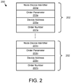
- FIG. 2 is a schematic block diagram of network data 200.
- the network data 200 may be used to determine the order of node devices 103 on the network cable 105 and to assign device addresses 205 to the node devices 103.
- the network data 200 may be organized as a data structure in a memory
- the network data 200 includes an entry 202 for each node device 103.
- Each entry 202 may include the node device identifier 201, an order parameter 203, the device address 205, and an order number 207.
- the node device identifier 201 may be a MAC address, a serial number, a custom identifier, and the like. Each node device identifier 201 may be unique. The node device identifier 201 may be used to address the corresponding node device 103.
- the order parameter 203 may be measured by the master device 101 in order to determine the order of the corresponding node device 103 on the network cable 105.
- the order parameter 203 is a node voltage that is measured at the node device 103.
- the order parameter 203 may be a node voltage of a data line 115 measured at the node device 103.
- the order parameter 203 may be a time-of-flight for a pulse that is transmitted on the data line 115 by the master device 101, returned as an answering pulse that is reflected by one and only one node device 103 or generated by one and only one node device 103, and received back at the master device 101.
- the order number 207 may indicate the place of the node device 103 on the network cable 105.
- Table 1 illustrates one embodiment of order numbers 207.
- Table 1 Device 101/103 Order Number 207 Master Device 101 0 First Node Device 103 1 Second Node Device 103 2 Third Node Device 103 3 Fourth Node Device 103 4
- the device address 205 may indicate the physical place of the node device 103 on the network cable 105.
- the device address 205 is an Internet Protocol (IP) address.
- IP Internet Protocol
- the IP address may be serial network unique.
- the IP address may be assigned sequentially beginning with the master device 101.
- Table 2 illustrates one embodiment of sequential IP address assignment Table 2 Device 101/103 Device Address 205 Master Device 101 192.168.1.0 First Node Device 103 192.168.1.1 Second Node Device 103 192.168.1.2 Third Node Device 103 192.168.1.3 Fourth Node Device 103 192.168.1.4
- Figure 3A is a schematic drawing of a master device 101 and a node device 103 on the serial network 100.
- the data lines 115 are shown.
- the master device 101 and one representative node device 103 are connected to the data lines 115.
- the master device 101 and the node device 103 each comprise a physical device 301 and/or a controller 303.
- the physical device 301 may be a switch, a control, a display, an indicator, an actuator, and the like.
- the physical device 301 may be connected to the data lines 115 via capacitors 315.
- the controller 303 may manage the corresponding master device 101 or node device 103.
- the physical device 301 and controller 303 may be configured based on the functions performed by the corresponding master device 101 and/or node device 103.
- the master device 101 includes a current source 305.
- the current source 305 may apply a current to the data lines 115 via current connections 321. In a certain embodiment, the current source 305 applies the current at a specified voltage.
- the current source 305 may apply the current in response to a current command 323 from the controller 303.
- the current command 323 may be an analog signal or a digital command.
- At least node device 103 may include a voltage circuit 313 as shown.
- the voltage circuit 313 may measure voltage between the data lines 115 at data line connections 325.
- the voltage circuit 313 may communicate the voltage to the controller 303 via a voltage signal 327.
- the voltage signal 327 may be a digital value.
- the voltage signal 327 may be an analog value that is converted to a digital value by an analog to digital converter at the controller 303.
- the controller 303 may communicate the digital value of the voltage as the order parameter 203 from the node device 103 to the master device 101.
- the controller 303 may communicate the node device identifier 201 with the order parameter 203 to the master device 101.
- the data lines 115 between the master device 101 and/or each node device 103 comprise at least one node component 307.
- Each node component 307 may present a constant Direct Current (DC) resistance in series with the data lines 115 of the serial network 100.
- the node component 307 is an inductor.
- the node component 307 may also be a resistor and/or a resistor/inductor combination.
- the node component 307 may have an inductance in the range of 20 to 80 nanohenries (nH).
- the node component 307 may be disposed inside a connector of the network cable 105.
- each node device 103 has a distinct voltage that is measured by the voltage circuit 313.
- each node device 103 reports a distinct, unique voltage to the master device 101, enabling the node voltage to identify the order of node devices 103 on the network cable 105.
- the current return path is not depicted, but may be through an end of line termination.
- Figure 3B is a schematic drawing of one embodiment of the current source 305 of Figure 3A .
- the current command 323 turns a current generator 319 on and off
- the current generator 319 applies the current to the data lines 115 via the current connections 321.
- one or more current inductors 317 are in series with the current generator 319.
- the current inductors 317 may have a constant DC resistance.
- the current source 305 may supply a voltage between the current connections 321.
- Figure 3C is a schematic drawing of one embodiment of the voltage circuit 313 of Figure 3A .
- the data line connections 325 are buffered by a protection circuit 331.
- An operational amplifier (op amp) 333 may measure the voltage at the data lines 115 and communicate the voltage signal 327 to the controller 303 of the node device 103.
- An analog to digital converter at the controller 303 may convert the voltage signal 327 to a digital node voltage.
- Figure 3D is a schematic drawing of the master device 101 and the node device 103 on the serial network 100.
- the master device 101 and the node device 103 are shown connected to the data lines 115 of the network cable 105.
- the physical device 301 is connected to the data lines 115 via capacitors 315.
- the node device 103 includes a low impedance circuit 311.
- the low impedance circuit 311 is connected to the data lines 115 via impedance connections 345a-b, In response to a low impedance command 349 from the controller 303, the low impedance circuit 311 may generate a low impedance such as the short across the data lines 115.
- the master device 101 includes a pulse circuit 309 that is connected to the data lines 115 via a pulse connection 341.
- the pulse circuit 309 may generate a pulse in response to a pulse command 353.
- the pulse circuit 309 may further detect an answering pulse that is a reflection of the pulse at the pulse connection 341 using a voltage threshold 343 as will be described hereafter.
- the pulse circuit 309 may measure a time-of-flight 363 of the pulse as a time interval from the generation of the pulse to the detection of the answering pulse.
- the pulse circuit 309 may communicate the time-of-flight 363 as the order parameter 203 to the controller 303.
- the data lines 115 between the master device 101 and/or each node device 103 comprise at least one node component 307.
- Each node component 307 may present a constant DC resistance in series with the data lines 115 of the serial network 100.
- the node component 307 is an inductor.
- the node component 307 may also be a resistor and/or a resistor/inductor combination.
- the node component 307 may have an inductance in the range of 20 to 80 nanohenries (nH).
- the node component 307 may increase the time-of-flight 363 measured between the node devices 103, increasing the differences between the order parameters 203.
- FIG. 3E is a schematic drawing of the pulse circuit 309.
- the pulse circuit 309 includes a pulse generator 361 that generates the pulse on a data line 115 via the pulse connection 341.
- the pulse command 353 initiates generation of the pulse and starts a timer 362.
- An op amp 335 compares the voltage of the data line 115 to the voltage threshold 343. If the voltage of the data line 115 exceeds the voltage threshold 343 a stop command 365 is generated by the op amp 335 that stops the timer 362.
- the voltage threshold 343 may be in the range of 0.5 to 1.5 volts.
- the time interval from the start of the timer 362 to stopping the timer 362 is the time-of-flight 363 of the pulse.
- FIG 3F is a schematic drawing of the low impedance circuit 311 of Figure 3D .
- the low impedance command 349 closes a switch 350 that shorts the impedance connections 345a-b.
- a low impedance component 352 is in series with the switch 350.
- the low impedance component 352 may have a resistance of less than 50 ohms.
- FIG. 3G is a schematic drawing of a master device 101 and a node device 103 on the serial network according 100.
- the node device 103 includes the pulse circuit 309.
- the pulse circuit 309 of the node device 103 detects the pulse 361a generated by the pulse circuit 309 of the master device 101.
- the controller 303 of the node device 103 directs the pulse circuit 309 of the node device 103 to generate a response pulse as the answering pulse 361b.
- the pulse circuit 309 of the master device 101 receives the answering pulse 361b.
- FIG 3H is a schematic drawing of the pulses 361 of Figure 3D and 3G .
- the pulse circuit 309 of the master device 101 generates a pulse 361a that travels over the data line 115.
- an answering pulse 361b that is a reflection of the pulse 361b is generated that returns to the pulse circuit 309 of the master device 101.
- an answering pulse 361b that is a response pulse generated by the pulse circuit 309 of the node device 103 is communicated to the pulse circuit 309 of the master device 101.
- the time interval between generating the pulse 361a at the pulse circuit 309 and receiving the answering pulse 361b at the pulse circuit 309 of the master device 101 is the time-of-flight 363.
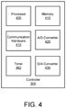
- FIG 4 is a schematic block diagram of the controller 303.
- the controller 303 includes a processor 405, a memory 410, and communication hardware 415.
- the memory 410 may be a semiconductor storage device, a hard disk drive, or combinations thereof.
- the memory 410 stores code.
- the processor 405 executes the code.
- the communication hardware 415 may communicate with other devices.
- the communication hardware 415 may communicate with the physical device 301.
- the communication hardware 415 may communicate with the data lines 115, In a certain embodiment, the communication hardware 415 communicates with a network such as an Ethernet network.
- the controller 303 includes the timer 362.
- the controller 303 may include an analog to digital converter 420 and/or a digital to analog converter 430.
- the analog-to-digital converter 420 may convert the voltage signal 327 to a digital value.
- the digital to analog converter 430 may generate the voltage threshold 343.
- Figure 5A is a schematic flow chart diagram of a device addressing method 500.
- the method 500 may generate the order parameter 203 and the order number 207 for each node device 103.
- the method 500 may generate the device address 205 for each node device 103.
- the method 500 may be performed by the controller 303 and/or processor 405 of the master device 101 and/or node devices 103.
- the method 500 starts, and in one embodiment, the processor 405 configures 501 each node device 103 on the serial network 100 for an order measurement.
- Configuring 501 each of the node devices 103 may comprise applying a specified current to the data lines 115 with the current source 305 and directing each node device 103 to report the node voltage as the order parameter 203 and a node device identifier 201. Determining the order number 207 using the node voltage is described in more detail in Figure 5C .
- configuring 501 each of node devices 103 comprises iteratively directing one of the node devices 103 to create a low impedance across data lines 115 of the serial network 100 with the low impedance circuit 311 and directing all other of the node devices 103 to create a high impedance across the data lines 115 with the low impedance circuit 311. Determining the order number 207 using the time-of-flight 363 is described in more detail in Figure 5B .
- the processor 405 further measures 503 the order parameter 203.
- Measuring the order parameter 203 may include receiving the node voltage as the order parameter 203 and receiving the node device identifier 201.
- measuring the order parameter 203 includes transmitting the pulse 361a over the data lines 115 from the pulse circuit 309, receiving an answering pulse 361b at the pulse circuit 309, and measuring the order parameter 203 as a time of flight 363 for the answering pulse 361b over the data lines 115 from transmitting the pulse to receiving the answering pulse 361b.
- the processor 405 may determine 505 the order number 207 of each of the node devices 103 based on the order parameter 203 for the node device 103.
- the order parameter 203 is the node voltage.
- the processor 405 may determine 505 the order number 207 by ranking the node voltages from highest to lowest node voltage.
- Table 3 illustrates one embodiment of determining 505 the order number 207 based on node voltages. Table 3 Node Voltage Order Number 207 4.5V 1 3.5V 2 2.5V 3 1.5V 4
- the processor 405 determines 505 the order number 207 by ranking the time-of-flight 363 for each node device 103 from shortest to longest time-of-flight 363.
- Table 4 illustrates one embodiment of determining 505 the order number 207 based on the time-of-flight 363 as measured in microseconds ( ⁇ s).
- Table 4 Time-of-Flight 363 Order Number 207 0.4 ⁇ s 1 0.7 ⁇ s 2 1.1 ⁇ s 3 1.4 ⁇ s 4
- the processor 405 assigns 507 a serial network unique and/or sequential device address 205 to each of the plurality of node devices 103 based on the order number 207 of the node device 103.
- the master device 101 may be assigned a first device address 205 and each subsequent node device 103 the assigned a serial network unique and/or sequential device address 205 based on the first device address 205.
- Table 5 illustrates one embodiment of assigning 507 serial network unique and/or sequential device addresses 205. Table 5 Order Number 207 Device Address 205 Master Device 101 192.168.1.0 1 192.168.1.1 2 192.168.1.2 3 192.168.1.3 4 192.168.1.4
- a node device 103 is configured based on the order number 207. In addition, the node device 103 may be configured based on the node device identifier 201. In a certain embodiment, the node device 103 is configured based on a function of the node device.
- the processor 405 may verify 508 at least one node device 103 based on the order number 207 for the node device 103. For example, the processor 405 may verify 508 that a correct node device 103 is at a location in the network cable 105 as indicated by the order number 207. In addition, the processor 405 may verify 508 a firmware version and/or manufacturer for at least one node device 103.
- the processor 405 further communicates 509 with one or more node devices 103 based on the device addresses 205 and the method 500 ends. For example, continuing the example of Table 5, the processor 405 may communicate 509 with the node device 103 at IP address 192.168.1.2.
- Figure 5B is a schematic flow chart diagram of a time-of-flight order determination method 550.
- the method 550 may generate the order parameter 203 and the order number 207 for each node device 103.
- the method 550 may be performed by the controller 303 and/or processor 405 of the master device 101 and/or node devices 103.
- the method 550 starts, and in one embodiment, the processor 405 selects 551 one and only one node device 103 of the plurality of node devices 103
- the processor 405 may iteratively select 551 each node device 103 in turn.
- the node devices 103 are selected based on the node device identifier 201.
- the processor 405 further directs 553 the selected node device 103 to communicate the answering pulse 361b.
- the processor 405 may direct 553 the selected node device 103 of Figure 3D to create a low impedance across data lines 115 to communicate the answering pulse 361b.
- the processor 405 asserts the low impedance command 349 at the selected node device 103. Asserting the low impedance command 349 may direct the low impedance circuit 311 to short the data lines 115. Alternatively, asserting the low impedance command 349 may direct the low impedance circuit 311 to lower the impedance between the data lines 115.
- the processor 405 directs 553 the selected node device 103 to generate a response pulse to communicate the answering pulse 361b.
- the processor 405 of the selected node device 103 of Figure 3G may receive the time-of-flight 363 from the timer 362 indicating that the pulse 361a was received.
- the processor 405 of the selected node device 103 may assert the pulse command 353 to generate the response pulse answering pulse 361b.
- the processor 405 further directs 555 all other of the node devices 103 not communicate the answering pulse 361b.
- the processor 405 may direct 555 the all other of the node devices 103 of Figure 3D to create a high impedance across the data lines 115.
- the processors 405 of the all other node devices 103 de-assert the low impedance command 349. De-asserting the low impedance command 349 may direct the low impedance circuit 311 to maintain the impedance between the data lines 115.
- the processor 405 may direct 555 all other node devices of Figure 3G to not generate the answering pulse 361b.
- the processor 405 further transmits 557 the pulse 361a over the data lines 115.
- the processor 405 issues the pulse command 353.
- the pulse circuit 309 may generate the pulse 361a.
- the pulse 361a is slowed by at least one node component 307.
- the pulse 361a is reflected by the low impedance circuit 311 of the selected node device 103 as the answering pulse 361b.
- the answering pulse 361b is generated by the pulse circuit 309 of the selected node device 103 as a response pulse.
- the pulse circuit 309 receives 559 the answering pulse 361b and measures 561 the time-of-flight 363 for the answering pulse 361b.
- the pulse circuit 309 may communicate the time-of-flight 363 to the processor 405 of the master device 101 as the order parameter 203.
- the time-of-flight 363 may be communicated in a standard format.
- the processor 405 determines 563 if the time-of-flight 363 for each node device 103 is measured. If all time-of-flights 363 are not measured, the processor 405 selects 551 a new device node 103. If all time-of-flights 363 are measured, the processor 405 determines 565 the order number 207 based on the order parameter 203 and the method 550 ends. For example, the order number 207 may be determined 565 as shown in Table 4.
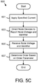
- Figure 5C is a schematic flow chart diagram of a node voltage order determination method 600.
- the method 600 may generate the order parameter 203 and the order number 207 for each node device 103.
- the method 600 may be performed by the controller 303 and/or processor 405 of the master device 101 and/or node devices 103.
- the method 600 starts, and in one embodiment, the processor 405 applies 601 a specified current to the data lines 115.
- the processor 405 may assert the voltage command 323. Asserting the voltage command 323 may activate the current generator 319.
- the processor 405 may further direct 603 each node device 103 to report a node voltage and a node device identifier 201. In one embodiment, the processor 405 directs 603 each node device 103 to go silent and not communicate with the data lines 115. The processor 405 may use the node device identifier 201 to direct 603 a specified node device 103 to measure the node voltage with the voltage circuit 313. The processor 405 may further direct 603 each node device 103 to measure the node voltage after a specified quiet time interval.
- the voltage circuit 313 may communicate the voltage signal 327 to the processor 405 of the node device 103.
- the controller 303 of the node device 103 may convert the voltage signal 327 to the node voltage and communicate the node voltage to the processor 405 of the master device 101 as the order parameter 203.
- the processor 405 iteratively directs 603 each node device 103 to report the node voltage.
- the processor 405 directs 603 all node devices 103 to report the node voltage.
- the node devices 103 may report the node voltage along with the node device identifier 201 for each node device 103.
- the processor 405 receives 605 the node voltage as the order parameter 203. In addition, the processor 405 may receive 605 the node device identifier 201 The order parameter 203 and/or node device identifier 201 may be received in a standard format.
- the processor 405 determines 607 the order number 207 based on the order parameter 203 and the method 600 ends.
- the order number 207 may be determined 607 as shown in Table 3.
- Node devices 103 are added to the network cable 105 of the serial network 100 to provide communications to the node devices 103. While each node device 103 may be logically identified and addressed based on the node device identifier 201, the physical order of node devices 103 on the network cable 105 may be unknown.
- the embodiments configure each node device 103 on the serial network 100 for an order measurement.
- the embodiments further measure the order parameter 203 for each of the node devices 103.
- the embodiments determine the order number 207 for each of the node devices 103 based on the order parameter 203 for the node device 103.
- the embodiments assign a serial network unique and/or sequential device address 205 to each of the node devices 103 based on the order number 207 of the node device 103.
- the physical order of the node devices 103 may be identified based on the device address 205.
- a node device 103 may be physical identified and/or located on the network cable 105.
Landscapes
- Engineering & Computer Science (AREA)
- Radar, Positioning & Navigation (AREA)
- Remote Sensing (AREA)
- Computer Networks & Wireless Communication (AREA)
- Signal Processing (AREA)
- Physics & Mathematics (AREA)
- General Physics & Mathematics (AREA)
- Computer Hardware Design (AREA)
- General Engineering & Computer Science (AREA)
- Dc Digital Transmission (AREA)
- Small-Scale Networks (AREA)
Applications Claiming Priority (1)
| Application Number | Priority Date | Filing Date | Title |
|---|---|---|---|
| US16/985,423 US20220043135A1 (en) | 2020-08-05 | 2020-08-05 | Automatic device ordering |
Publications (1)
| Publication Number | Publication Date |
|---|---|
| EP3961998A1 true EP3961998A1 (de) | 2022-03-02 |
Family
ID=77249664
Family Applications (1)
| Application Number | Title | Priority Date | Filing Date |
|---|---|---|---|
| EP21185483.1A Withdrawn EP3961998A1 (de) | 2020-08-05 | 2021-07-14 | Automatische vorrichtungsordnung |
Country Status (2)
| Country | Link |
|---|---|
| US (2) | US20220043135A1 (de) |
| EP (1) | EP3961998A1 (de) |
Families Citing this family (2)
| Publication number | Priority date | Publication date | Assignee | Title |
|---|---|---|---|---|
| US20220043135A1 (en) * | 2020-08-05 | 2022-02-10 | Rockwell Automation Technologies, Inc. | Automatic device ordering |
| CN120917392A (zh) * | 2023-04-04 | 2025-11-07 | 西门子瑞士有限公司 | I/o模块的高效替换 |
Citations (4)
| Publication number | Priority date | Publication date | Assignee | Title |
|---|---|---|---|---|
| US9934191B2 (en) * | 2014-07-31 | 2018-04-03 | Neofocal Systems, Inc. | Systems and methods for assigning addresses to serially arranged circuit nodes |
| WO2019166503A2 (de) * | 2018-02-27 | 2019-09-06 | Elmos Semiconductor Aktiengesellschaft | Datenbussystem und vergabe von busadressen in einem derartigen datenbussystem |
| EP3419225B1 (de) * | 2017-06-21 | 2020-03-18 | Nxp B.V. | System und verfahren zur ermöglichung der bestimmung der relativen positionen von slave-einheiten entlang eines stich-busses |
| WO2020088968A1 (en) * | 2018-10-29 | 2020-05-07 | Signify Holding B.V. | System for providing a sequence of nodes in a network |
Family Cites Families (20)
| Publication number | Priority date | Publication date | Assignee | Title |
|---|---|---|---|---|
| US3733602A (en) | 1971-05-20 | 1973-05-15 | Motorola Inc | Microwave intrusion detecting system and apparatus |
| US6542946B1 (en) * | 2000-01-28 | 2003-04-01 | Compaq Information Technologies Group, L.P. | Dual mode differential transceiver for a universal serial bus |
| DE10048745C1 (de) * | 2000-09-29 | 2002-02-21 | Siemens Ag | Verfahren und Vorrichtung zur Ermittlung der Netztopologie eines Bussystems |
| DE10337699B4 (de) * | 2003-08-16 | 2006-01-12 | Phoenix Contact Gmbh & Co. Kg | Verfahren und Vorrichtung zur Übertragung von Daten über ein Busnetz unter Verwendung des Broadcast-Prinzip |
| US7233164B2 (en) | 2003-12-17 | 2007-06-19 | Rambus Inc. | Offset cancellation in a multi-level signaling system |
| KR100677754B1 (ko) * | 2005-03-11 | 2007-02-02 | 삼성전자주식회사 | 무선 센서 네트워크에서의 아이디 생성방법 및 등록방법 |
| US7486104B2 (en) * | 2006-06-02 | 2009-02-03 | Rambus Inc. | Integrated circuit with graduated on-die termination |
| US8446856B2 (en) | 2008-12-19 | 2013-05-21 | Research In Motion Limited | System and method for relay node selection |
| US8988102B2 (en) * | 2011-02-02 | 2015-03-24 | Rambus Inc. | On-die termination |
| JP5838821B2 (ja) | 2012-01-16 | 2016-01-06 | 住友電装株式会社 | コネクタセットの固定方法 |
| US9475093B2 (en) | 2013-10-03 | 2016-10-25 | Fujifilm Dimatix, Inc. | Piezoelectric ultrasonic transducer array with switched operational modes |
| CN108370258B (zh) | 2015-09-10 | 2020-07-10 | 蓝色多瑙河系统有限公司 | 校准串行互连 |
| US9960981B2 (en) * | 2015-10-08 | 2018-05-01 | Sony Corporation | Communication device, communication method, program, and communication system |
| US11294051B2 (en) | 2017-05-02 | 2022-04-05 | Creative Racing Products, LLC | Ultrasonic measurement device |
| US11079461B2 (en) * | 2019-03-11 | 2021-08-03 | Vaisala, Inc. | Consistent arrival time measurement and determination of discharge polarity |
| US11402476B2 (en) * | 2019-03-20 | 2022-08-02 | Microvision, Inc. | Method and apparatus for LIDAR channel encoding |
| DE102019212415A1 (de) * | 2019-08-20 | 2021-02-25 | Conti Temic Microelectronic Gmbh | Verfahren zur Positionserkennung eines Busteilnehmers |
| US11714183B2 (en) * | 2019-09-03 | 2023-08-01 | Nxp B.V. | Impulse radar using variable pulse repetition frequency |
| KR102695147B1 (ko) * | 2020-04-13 | 2024-08-13 | 삼성전기주식회사 | 프론트-엔드 모듈 |
| US20220043135A1 (en) * | 2020-08-05 | 2022-02-10 | Rockwell Automation Technologies, Inc. | Automatic device ordering |
-
2020
- 2020-08-05 US US16/985,423 patent/US20220043135A1/en not_active Abandoned
-
2021
- 2021-07-14 EP EP21185483.1A patent/EP3961998A1/de not_active Withdrawn
-
2023
- 2023-01-27 US US18/160,517 patent/US12335228B2/en active Active
Patent Citations (4)
| Publication number | Priority date | Publication date | Assignee | Title |
|---|---|---|---|---|
| US9934191B2 (en) * | 2014-07-31 | 2018-04-03 | Neofocal Systems, Inc. | Systems and methods for assigning addresses to serially arranged circuit nodes |
| EP3419225B1 (de) * | 2017-06-21 | 2020-03-18 | Nxp B.V. | System und verfahren zur ermöglichung der bestimmung der relativen positionen von slave-einheiten entlang eines stich-busses |
| WO2019166503A2 (de) * | 2018-02-27 | 2019-09-06 | Elmos Semiconductor Aktiengesellschaft | Datenbussystem und vergabe von busadressen in einem derartigen datenbussystem |
| WO2020088968A1 (en) * | 2018-10-29 | 2020-05-07 | Signify Holding B.V. | System for providing a sequence of nodes in a network |
Non-Patent Citations (1)
| Title |
|---|
| "IEEE 802.3 SPMD 10SPE Multidrop Enhancements Study Group OBJECTIVES FOR THE ELEVATOR/ESCALATOR AND AUTOMOTIVE SEGMENTS TOPOLOGY DISCOVERY (RANGING)", vol. 802.3.SPMD;802.3da, 21 January 2020 (2020-01-21), pages 1 - 16, XP068168656, Retrieved from the Internet <URL:http://www.ieee802.org/3/SPMD/public/jan20/Huszak_01a_SPMD_0120.pdf> [retrieved on 20200121] * |
Also Published As
| Publication number | Publication date |
|---|---|
| US20230168357A1 (en) | 2023-06-01 |
| US12335228B2 (en) | 2025-06-17 |
| US20220043135A1 (en) | 2022-02-10 |
Similar Documents
| Publication | Publication Date | Title |
|---|---|---|
| US12335228B2 (en) | Automatic device ordering | |
| US8099469B2 (en) | Master nodes and slave nodes for a communication network, and methods thereof | |
| GB2397712A (en) | Transceiver with memory for failure information storage | |
| EP1697802B1 (de) | Verfahren und system zum automatisierten konfigurieren eines hart-mehrfachauskopplungssystems | |
| CN112956160B (zh) | 用于在网络中提供节点序列的系统 | |
| CN105337796B (zh) | 一种wifi路由器性能测试方法及系统 | |
| CN110492907B (zh) | 用于电表建立档案的方法及装置 | |
| CN112671584B (zh) | 网络拓扑的识别方法、装置、系统和存储介质 | |
| US10313301B1 (en) | Intellectual rack and IP addresses managing method thereof | |
| US11240068B2 (en) | Method for detecting and identifying items of equipment communicating according to a Modbus protocol and communication controller for the implementation of such a method | |
| EP3016351B1 (de) | Verfahren zum Betrieb einer Sensoranordnung mit mehreren Sensorvorrichtungen, Sensorvorrichtung, Sensoranordnung und Sensorsystem | |
| CN104487802A (zh) | 测量机器通信 | |
| CA3112110A1 (en) | Method of assigning addresses to bus participants | |
| CN111694779A (zh) | 接口切换装置、通信设备及接口切换方法 | |
| KR100619424B1 (ko) | 동적 번랙 모니터 리스너 서버 | |
| CN106453012B (zh) | 一种串行总线通信方法及装置 | |
| CN118748671A (zh) | 一种自动寻址电路、自动寻址系统及自动寻址方法 | |
| US11570140B1 (en) | Detecting and correcting colliding media access control addresses | |
| CN115292112A (zh) | 从机设备的检测方法、装置、存储介质及电子装置 | |
| US9325574B2 (en) | Method and configuration component for assigning a station name to components of an industrial automation arrangement | |
| KR102434128B1 (ko) | Plc 시스템 | |
| CN115914025B (zh) | 基于蓝牙mesh的产品自动联网的测试方法 | |
| TW202024915A (zh) | 基於測試狀態的燈控系統及其方法 | |
| JPH0328102B2 (de) | ||
| CN103780456B (zh) | 对ttcn‑3测试系统进行适配性配置的方法和装置 |
Legal Events
| Date | Code | Title | Description |
|---|---|---|---|
| PUAI | Public reference made under article 153(3) epc to a published international application that has entered the european phase |
Free format text: ORIGINAL CODE: 0009012 |
|
| STAA | Information on the status of an ep patent application or granted ep patent |
Free format text: STATUS: THE APPLICATION HAS BEEN PUBLISHED |
|
| AK | Designated contracting states |
Kind code of ref document: A1 Designated state(s): AL AT BE BG CH CY CZ DE DK EE ES FI FR GB GR HR HU IE IS IT LI LT LU LV MC MK MT NL NO PL PT RO RS SE SI SK SM TR |
|
| STAA | Information on the status of an ep patent application or granted ep patent |
Free format text: STATUS: REQUEST FOR EXAMINATION WAS MADE |
|
| 17P | Request for examination filed |
Effective date: 20220802 |
|
| RBV | Designated contracting states (corrected) |
Designated state(s): AL AT BE BG CH CY CZ DE DK EE ES FI FR GB GR HR HU IE IS IT LI LT LU LV MC MK MT NL NO PL PT RO RS SE SI SK SM TR |
|
| STAA | Information on the status of an ep patent application or granted ep patent |
Free format text: STATUS: EXAMINATION IS IN PROGRESS |
|
| 17Q | First examination report despatched |
Effective date: 20240124 |
|
| STAA | Information on the status of an ep patent application or granted ep patent |
Free format text: STATUS: THE APPLICATION HAS BEEN WITHDRAWN |
|
| 18W | Application withdrawn |
Effective date: 20240403 |