EP3961920B1 - Leseverstärkerschaltung - Google Patents
Leseverstärkerschaltung Download PDFInfo
- Publication number
- EP3961920B1 EP3961920B1 EP20193019.5A EP20193019A EP3961920B1 EP 3961920 B1 EP3961920 B1 EP 3961920B1 EP 20193019 A EP20193019 A EP 20193019A EP 3961920 B1 EP3961920 B1 EP 3961920B1
- Authority
- EP
- European Patent Office
- Prior art keywords
- output
- amplification
- terminal
- stage
- block
- Prior art date
- Legal status (The legal status is an assumption and is not a legal conclusion. Google has not performed a legal analysis and makes no representation as to the accuracy of the status listed.)
- Active
Links
Images






Classifications
-
- H—ELECTRICITY
- H03—ELECTRONIC CIRCUITRY
- H03F—AMPLIFIERS
- H03F3/00—Amplifiers with only discharge tubes or only semiconductor devices as amplifying elements
- H03F3/20—Power amplifiers, e.g. Class B amplifiers, Class C amplifiers
- H03F3/21—Power amplifiers, e.g. Class B amplifiers, Class C amplifiers with semiconductor devices only
- H03F3/217—Class D power amplifiers; Switching amplifiers
- H03F3/2171—Class D power amplifiers; Switching amplifiers with field-effect devices
-
- H—ELECTRICITY
- H03—ELECTRONIC CIRCUITRY
- H03F—AMPLIFIERS
- H03F3/00—Amplifiers with only discharge tubes or only semiconductor devices as amplifying elements
- H03F3/181—Low-frequency amplifiers, e.g. audio preamplifiers
- H03F3/183—Low-frequency amplifiers, e.g. audio preamplifiers with semiconductor devices only
-
- H—ELECTRICITY
- H03—ELECTRONIC CIRCUITRY
- H03F—AMPLIFIERS
- H03F1/00—Details of amplifiers with only discharge tubes, only semiconductor devices or only unspecified devices as amplifying elements
- H03F1/32—Modifications of amplifiers to reduce non-linear distortion
- H03F1/3205—Modifications of amplifiers to reduce non-linear distortion in field-effect transistor amplifiers
-
- H—ELECTRICITY
- H03—ELECTRONIC CIRCUITRY
- H03F—AMPLIFIERS
- H03F1/00—Details of amplifiers with only discharge tubes, only semiconductor devices or only unspecified devices as amplifying elements
- H03F1/52—Circuit arrangements for protecting such amplifiers
- H03F1/523—Circuit arrangements for protecting such amplifiers for amplifiers using field-effect devices
-
- H—ELECTRICITY
- H03—ELECTRONIC CIRCUITRY
- H03F—AMPLIFIERS
- H03F3/00—Amplifiers with only discharge tubes or only semiconductor devices as amplifying elements
- H03F3/181—Low-frequency amplifiers, e.g. audio preamplifiers
- H03F3/183—Low-frequency amplifiers, e.g. audio preamplifiers with semiconductor devices only
- H03F3/185—Low-frequency amplifiers, e.g. audio preamplifiers with semiconductor devices only with field-effect devices
-
- H—ELECTRICITY
- H03—ELECTRONIC CIRCUITRY
- H03F—AMPLIFIERS
- H03F3/00—Amplifiers with only discharge tubes or only semiconductor devices as amplifying elements
- H03F3/20—Power amplifiers, e.g. Class B amplifiers, Class C amplifiers
- H03F3/21—Power amplifiers, e.g. Class B amplifiers, Class C amplifiers with semiconductor devices only
- H03F3/217—Class D power amplifiers; Switching amplifiers
- H03F3/2173—Class D power amplifiers; Switching amplifiers of the bridge type
-
- H—ELECTRICITY
- H04—ELECTRIC COMMUNICATION TECHNIQUE
- H04R—LOUDSPEAKERS, MICROPHONES, GRAMOPHONE PICK-UPS OR LIKE ACOUSTIC ELECTROMECHANICAL TRANSDUCERS; ELECTRIC HEARING AIDS; PUBLIC ADDRESS SYSTEMS
- H04R3/00—Circuits for transducers
-
- H—ELECTRICITY
- H04—ELECTRIC COMMUNICATION TECHNIQUE
- H04R—LOUDSPEAKERS, MICROPHONES, GRAMOPHONE PICK-UPS OR LIKE ACOUSTIC ELECTROMECHANICAL TRANSDUCERS; ELECTRIC HEARING AIDS; PUBLIC ADDRESS SYSTEMS
- H04R3/00—Circuits for transducers
- H04R3/007—Protection circuits for transducers
-
- H—ELECTRICITY
- H03—ELECTRONIC CIRCUITRY
- H03F—AMPLIFIERS
- H03F2200/00—Indexing scheme relating to amplifiers
- H03F2200/03—Indexing scheme relating to amplifiers the amplifier being designed for audio applications
-
- H—ELECTRICITY
- H03—ELECTRONIC CIRCUITRY
- H03F—AMPLIFIERS
- H03F2200/00—Indexing scheme relating to amplifiers
- H03F2200/351—Pulse width modulation being used in an amplifying circuit
-
- H—ELECTRICITY
- H03—ELECTRONIC CIRCUITRY
- H03F—AMPLIFIERS
- H03F2200/00—Indexing scheme relating to amplifiers
- H03F2200/393—A measuring circuit being coupled to the output of an amplifier
-
- H—ELECTRICITY
- H03—ELECTRONIC CIRCUITRY
- H03F—AMPLIFIERS
- H03F2200/00—Indexing scheme relating to amplifiers
- H03F2200/456—A scaled replica of a transistor being present in an amplifier
-
- H—ELECTRICITY
- H03—ELECTRONIC CIRCUITRY
- H03F—AMPLIFIERS
- H03F2200/00—Indexing scheme relating to amplifiers
- H03F2200/462—Indexing scheme relating to amplifiers the current being sensed
-
- H—ELECTRICITY
- H03—ELECTRONIC CIRCUITRY
- H03F—AMPLIFIERS
- H03F2200/00—Indexing scheme relating to amplifiers
- H03F2200/481—A resistor being used as sensor
-
- H—ELECTRICITY
- H04—ELECTRIC COMMUNICATION TECHNIQUE
- H04R—LOUDSPEAKERS, MICROPHONES, GRAMOPHONE PICK-UPS OR LIKE ACOUSTIC ELECTROMECHANICAL TRANSDUCERS; ELECTRIC HEARING AIDS; PUBLIC ADDRESS SYSTEMS
- H04R29/00—Monitoring arrangements; Testing arrangements
- H04R29/001—Monitoring arrangements; Testing arrangements for loudspeakers
Definitions
- the present disclosure relates to load sense amplifier circuits and output stages that use such sense amplifier circuits.
- US 2016/065134 A1 describes an amplifier circuit having an output stage that includes an H-bridge circuit.
- the H-bridge circuit includes sense resistors on one side of the circuit.
- a current detection circuit can produce an output indicative of current flow through a load based on voltages across the sense resistors.
- EP 3179631 A1 describes a class-D audio-amplifier apparatus including a circuit for reading a load current supplied by said amplifier to a load, said amplifier comprising a final stage, which includes a full-H bridge comprising a first half-bridge and a second half-bridge; said circuit being configured for estimating said load current through reading of a current supplied by at least one power transistor, by measuring a drain-to-source voltage thereof during an ON period.
- Said apparatus comprises a sensing circuit connected for detecting a first drain-to-source voltage from a transistor of the first half-bridge and a second drain-to-source voltage from a corresponding transistor of the second half-bridge, said sensing circuit comprising: a module for computing a difference between said first detected drain-to-source voltage and said second detected drain-to-source voltage; and a module for performing an averaging operation on said difference to obtain a sense voltage value to be supplied to an analog-to-digital converter.
- US 2016/0182998 A1 describes a method for speaker operation comprises sensing an input common mode signal of a driver, wherein the driver drives a speaker, and adjusting the input common mode signal of the driver based on a difference between the sensed input common mode signal and a reference signal.
- the method also comprises sensing a current of a coil of the speaker, and controlling an output volume of the speaker based at least in part on the sensed current.
- US 2018/0014119 A1 describes a class-D amplifier that includes two high-side transistors, two low-side transistors, a first sense resistor, a second sense resistor, and a sigma delta analog to digital converter ( ⁇ ADC).
- the two high-side transistors and two low-side transistors are connected as a bridge to drive a bridge tied speaker.
- the first sense resistor is connected between a first of the low-side transistors and a low-side reference voltage.
- the second sense resistor is connected between a second of the low-side transistors and the low-side reference voltage.
- the ⁇ ADC is coupled to the bridge to measure voltage across the first sense resistor and the second sense resistor.
- a sense amplifier circuit comprising:
- Such a sense amplifier circuit can combine four-quadrant signals that are received at the four input-voltage-terminals into a single differential voltage signal. This may simplify and improve the accuracy of current sensing measurements in an output stage such as a class-D output stage.
- each amplification-block-transistor is a bipolar-junction-transistor, BJT, or a field-effect-transistor, FET.
- the transistors of the first- and third-amplification-blocks are p-type metal-oxide-semiconductor FETs, MOSFETs.
- the transistors of the second- and fourth-amplification-blocks may be n-type MOSFETs.
- the sense amplifier circuit comprises a first-reference-voltage-terminal connected to the first-bias-voltage-source, and a second-reference-voltage-terminal connected to the second-bias-voltage-source.
- each amplification-block comprises a connection-node connected in series between the amplification-block-resistor and the first-conduction-channel-terminal.
- Each amplification-block may also comprise an amplifier comprising: an amplifier-first-input-terminal; an amplifier-second-input-terminal; and an amplifier-output-terminal.
- the amplifier-first-input-terminal may be connected to the amplification-block-control-node.
- the amplifier-second-input-terminal may be connected to the connection-node.
- the amplifier-output-terminal may be connected to the control-terminal. In this way, the control-terminal may be connected to the amplification-block-control-node via the amplifier.
- the first and third-amplification-blocks comprise an amplification-block-cascode-control-node.
- the first and third-amplification-blocks may also comprise a cascode connected in series between the second-conduction-channel-terminal and the amplification-block-output-node.
- the cascode may comprise a cascode-transistor comprising: a cascode-transistor-first-conduction-channel-terminal connected to the second-conduction-channel-terminal, a cascode-transistor-second-conduction-channel-terminal connected to the amplification-block-output-node, and a cascode-transistor-control-terminal connected to the amplification-block-cascode-control-node.
- the first and third-amplification-blocks may also comprise a cascode-diode comprising: a cascode-diode-anode connected to the cascode-transistor-second-conduction-channel-terminal, and a cascode-diode-cathode connected to the cascode-transistor-first-conduction-channel-terminal.
- the sense amplifier circuit comprises a third-bias-voltage-source connected to the amplification-block-cascode-control-node of the first- and third-amplification-blocks.
- each cascode-transistor is a p-type MOSFET.
- the third-bias-voltage-source is connected to the first-reference-voltage-terminal.
- the second-bias-voltage-source comprises: a second-bias-voltage-source-output-node connected to the amplification-block-control-nodes of the second- and fourth- amplification-blocks.
- the second-bias-voltage-source may also comprise a third-bias-voltage-source and / or a fifth-amplifier.
- the fifth-amplifier may comprise: an amplifier-first-input-terminal connected to the common-mode-voltage-node; an amplifier-second-input-terminal connected to the third-bias-voltage-source; and an amplifier-output-terminal connected to the second-bias-voltage-source-output-node.
- an output stage comprising:
- the output stage comprises a loudspeaker connected to the first- and second-output-device-terminals.
- the first-low-pass-filter and the second-low-pass-filter comprise an inductor-capacitor, LC, circuit.
- each first-output-stage-transistor and each second-output-stage-transistor is a field-effect-transistor, FET.
- Class-D audio amplifiers are widely applied for driving loudspeakers in consumer, mobile and automotive (e.g., car) audio systems.
- Figure 1 shows an example output stage 100 that corresponds to a class-D output stage found in car audio systems.
- the output stage 100 comprises a loudspeaker 101, first- and second-reference-voltage-terminals 102, 103 (V SUP and ground respectively), first- and second-output-voltage terminals 104, 105 (OUT p and OUT m respectively), first-, second-, third- and fourth-low-ohmic-powerFETs 106a-d, first-, second-, third- and fourth-diodes 107a-d, and first- and second-external-inductor-capacitor-filters (first- and second-external-LC-filters) 108a,b.
- the output stage 100 has a so-called Bridge-Tied-Load (BTL) configuration where both sides of the loudspeaker 101 are driven in opposite phase.
- the first- and second-output-nodes 104, 105 are alternatingly switched between the first-reference-voltage-terminal 102 and the second-reference-voltage-terminal 103 by the four low-ohmic-powerFETs 106a-d. This yields two square-wave signals with a fundamental frequency that typically lies around 500kHz.
- PWM pulse-width modulation
- the loudspeaker 101 is connected to the first- and second-output-terminals 104, 105 with the first- and second-external-LC-filters 108a,b. These filters suppress highfrequency components of the square-wave signals and only allow audio frequency components to pass.
- an audio amplifier such as the output stage shown in Figure 1
- the purpose of an audio amplifier is to force a voltage across a loudspeaker that reproduces an audio input signal with high fidelity. This means that the audio amplifier should not distort the audio input signal. Low distortion is in general achieved by applying feedback.
- a proper feedback loop has high loop gain in the audio frequency range that suppresses nonlinearity of the output stage and, optionally, the first- and second-external-LC-filters.
- the current delivered by the audio amplifier is determined by the loudspeaker impedance. There are many applications where it is necessary to measure or sense this current (the load current) with different requirements on the accuracy:
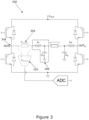
- Figure 2 shows an example of an output stage 200 configured for current sensing.
- the output stage 200 is similar to the output stage of Figure 1 in that it comprises a loudspeaker 201 and a first-external-LC-filter 208. Differences over the output stage of Figure 1 include a sense-resistor, R SENSE , 209 connected in series between the loudspeaker 201 and the first-external-LC-filter 208, a sense-amplifier, A SENSE , 210 configured to sense a voltage across the sense-resistor 209 (as shown, using pins 211a, 211b) and output an amplified voltage, and an analogue-to-digital converter, ADC, 212 connected to the sense-amplifier 210 such that it can receive the amplified voltage.
- R SENSE sense-resistor
- a SENSE analogue-to-digital converter
- the output stage 200 of Figure 2 may be considered to represent a straightforward and accurate configuration for current sensing. This is because the sense-resistor 209 is directly in series with the loudspeaker 201. In turn, a voltage across the sense-resistor 209 is sensed and amplified by the sense-amplifier 210 and then fed to the ADC 212. For accurate current sensing, the sense-amplifier 210 needs to have a very high common-mode rejection since the differential signal across the sense-resistor 209 is small, e.g. 50mV, whereas the signal swing at the loudspeaker 201 is much bigger, e.g. 25V.
- Figure 3 shows a further example of an output stage 300 configured for current sensing that is similar to the output stages of Figures 1 and 2 .
- the output-stage 300 comprises an first-output-voltage-terminal 304 (OUT p ), an first-external-LC-filter 308, a sense-resistor 309, and a sense-amplifier 310.
- a difference over the output stage of Figure 2 is that the sense-resistor 309 is placed upstream of the first-external-LC-filter 308 such that it is connected in series between the first-external-LC-filter 308 and the first-output-voltage-terminal 304. In principle, this configuration can be realized with without the need of additional pins.
- the implementation of the sense-amplifier 310 will be more challenging than in case shown in Figure 2 since now the common-mode voltage is the unfiltered switching output voltage, which is a PWM square-wave, instead of an audio signal. Furthermore, the current through the sense-resistor 309 is now the sum of the load current and the current through the capacitor C in the first-external-LC-filter 308.
- FIG. 4 shows a further example of an output stage 400 configured for current sensing.
- the output stage 400 comprises first- and second-low-side powerFETs 406b, 406d, a second-reference-voltage-terminal 403 (ground in this example), first- and second-sense-resistors 409a, 409b, a sense-amplifier 410, an analogue-to-digital converter, ADC, 412 and a low-pass filter (LPF) 413.
- first- and second-low-side powerFETs 406b, 406d a second-reference-voltage-terminal 403 (ground in this example)
- first- and second-sense-resistors 409a, 409b a sense-amplifier 410
- an analogue-to-digital converter ADC
- 412 and a low-pass filter
- the output stage 400 of Figure 4 represents an alternative configuration in which the first- and second-sense-resistors 409a, 409b are connected in series between the low-side powerFETs 406b, 406d and the second-reference-voltage-terminal 403.
- the common-mode rejection requirement of the sense-amplifier 410 can be relaxed because one terminal of each sense-resistor 409a, 409b is connected to the reference-voltage-terminal 403 (i.e., one terminal of each sense-resistor is grounded).
- the load and capacitor currents only flow through a given sense-resistor when a corresponding low-side powerFET is on (e.g., the sense-resistor 409a and the low-side powerFET 406b that are to the left of the second-reference-voltage-terminal 403).
- a corresponding low-side powerFET e.g., the sense-resistor 409a and the low-side powerFET 406b that are to the left of the second-reference-voltage-terminal 403
- the output stage of Figure 4 can be used in smart-speaker drivers in mobile applications, can be integrated without any external components or additional pins, and has only moderate requirements on the sense-amplifier 410.
- the output power levels are modest, e.g. less than 5W, which makes it feasible to place the sense-resistors in series with the low-side powerFETs that support all of the output current.
- the output-stage of Figure 4 may be unsuitable since the powerFETs are typically connected with several bondwires that are distributed along the perimeter of the powerFETs to make the current density as uniform as possible. In these cases it is impractical to route all current through a single sense resistor.
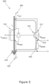
- Figure 5 shows an example circuit 500 that, in general terms, is configured for sensing not all current but only a fraction.
- the circuit 500 comprises an output-voltage terminal 504, a reference-voltage terminal (ground in this example) 503, a first-powerFET 514, which may correspond to a lowside powerFET in the output-stage of Figure 4 , M PWR0 , a second-powerFET 515, M PWR1 , comprising a source-terminal 516 and a drain-terminal 517, and a sense-resistor 509 connected in series between the source-terminal 516 and the reference-voltage-terminal 503.
- Figure 5 also shows graphically a representation of drain-current, I D , 518 from the voltage-output-terminal 504 to the voltage-reference-terminal 503.
- the circuit 500 corresponds to a case where a powerFET is 'split-up' into a 'larger part' (i.e., the first-powerFET 514) and a 'smaller part' (i.e., the second-powerFET 515) that has a sense-resistor 509 in series with the source-terminal 516.
- a powerFET is 'split-up' into a 'larger part' (i.e., the first-powerFET 514) and a 'smaller part' (i.e., the second-powerFET 515) that has a sense-resistor 509 in series with the source-terminal 516.
- the drain current 518 distributes between the first- and second-powerFETs 514, 515 in two fractions with the same ratio as the sizes (for example of the channel widths) of the first- and second-powerFETs 514, 515.
- the sense-circuit 500 in Figure 5 has one terminal of the sense-resistor 509 connected to ground.
- the common-mode rejection requirement of a sense-amplifier (not shown in Figure 5 ) is relaxed. This relaxation, however, is only true for lowside powerFETs that are connected to ground.
- the source is connected to the switching output node (compare to the first- and third-low-ohmic-powerFETS in the output-stage of Figure 1 ), which can result in unacceptably high common-mode swings.
- FIG. 6 shows a further example of a circuit 600 that is similar to the circuit of Figure 5 .
- the circuit 600 comprises a reference-voltage-terminal 602 (V SUP in this example), a sense-resistor 609, and a second-powerFET 615 comprising a drain-terminal 617.
- V SUP reference-voltage-terminal
- the sense-resistor 609 of the circuit 600 of Figure 6 is connected in series between the reference-voltage-terminal 602 and the drain-terminal 617. This configuration may address the problem of unacceptable common-mode swings described above.
- the sense-resistor can be placed in series with the source- or drain-terminal of a powerFET, so long as the resistance of the sense-resistor is small compared to the on-resistance of the 'smaller part' second-powerFET.
- a design trade-off needs to be made: a smaller resistance of the sense-resistor improves linearity but yields a smaller signal which deteriorates the Signal-to-Noise ratio (SNR) of the system.
- SNR Signal-to-Noise ratio
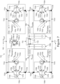
- Figure 7 shows an example embodiment of an output stage 700 that is based on the circuits of Figures 6 and 7 .
- the output stage 700 represents an alternative approach to current sensing than the approaches described with respect to the output stages shown in Figures 2-4 .
- the output stage 700 comprises an output-stage-first-reference-voltage-terminal (that receives a supply voltage, V SUP , in this example) 702, an output-stage-second-reference-voltage-terminal (that corresponds to ground, GND, in this example) 703, an output-stage-first-output-voltage-terminal (that outputs a positive output voltage, V OUTP , in this example) 704, and an output-stage-second-output-voltage-terminal (that outputs a negative output voltage, V OUTM , in this example) 705.
- a loudspeaker 701 can be connected between the output-stage-first-output-voltage-terminal V OUTP 704 and the output-stage-second-output-voltage-terminal V OUTM 705
- the output stage 700 further comprises a first-output-device-terminal 719 for connecting to an output device, which in this example is the loudspeaker 701, and a second-output-device-terminal 720.
- the output stage 700 further comprises a first-low-pass-circuit 708a connected in series between the first-output-device-terminal 719 and the output-stage-first-output-voltage-terminal 704, and a second-low-pass-circuit 708b connected in series between the second-output-device-terminal 720 and the output-stage-second-output-voltage-terminal 705.
- the first- and second-low-pass circuits 708a-b may be provided as inductor-capacitor, LC, circuits, or resistor-capacitor, RC, circuits.
- the output stage 700 is shown in Figure 7 comprising the loudspeaker 701 connected to the first- and second-output-device-terminals 719, 720, it will be appreciated that other components / output devices can be used instead of the loudspeaker 701.
- the output stage 700 further comprises first-, second-, third- and fourth-output-stage-amplification-blocks 721a-d.
- Each output-stage-amplification-block 721a-d comprises an output-stage-amplification-block-input-node 722a-d, an output-stage-amplification-block-output-node 723a-d, an output-stage-amplification-block-control-terminal 724a-d, an output-stage-amplification-block-sense-terminal 725a-d.
- each output-stage-amplification-block 721a-d also comprises an optional output-stage-amplification-block-reference-terminal 726a-d.
- each output-stage-amplification-block-sense-terminal 725a-d facilitates fractional sensing of current through the output stage 700A.
- Each output-stage-amplification-block 721a-d further comprises a first-output-stage-transistor 727a-d.
- the first-output-stage-transistors 727a-d comprise a first-output-stage-transistor-first-terminal 728a-d connected to the output-stage-amplification-block-input-node 722a-d, a first-output-stage-transistor-second-terminal 729a-d connected to the output-stage-amplification-block-output-node 723a-d, and a first-output-stage-transistor-control-terminal 730a-d connected to the output-stage-amplification-block-control-terminal 724a-d.
- the first-output-stage-transistor 727a-d is be a field-effect-transistor, FET, such as a metal-oxide semiconductor FET, MOSFET, or a powerFET, or a bipolar junction transistor or an insulated-gate bipolar transistor (IGBT).
- FET field-effect-transistor
- MOSFET metal-oxide semiconductor FET
- MOSFET metal-oxide semiconductor field-effect transistor
- IGBT insulated-gate bipolar transistor
- the MOSFET may be an n-type MOSFET or a p-type MOSFET.
- Each output-stage-amplification-block 721a-d further comprises a first-output-stage-diode 731a-d comprising a first-output-stage-diode-anode 732a-d connected to first-output-stage-transistor-second-terminal 729a-d, and a first-output-stage-diode-cathode 732a-d connected to the first-output-stage-transistor-first-terminal 728a-d.
- the first-output-stage-diodes 731a-d are body diodes of the associated first-output-stage-transistors 727a-d, such that the diodes are internal to the powerFET.
- the first-output-stage-diodes 731a-d can be included by lithographic construct of the device, and can be deliberately made to be significant so as to protect the first-output-stage-transistors 727a-d from damage against reverse recovery current during high frequency PWM switching. This can occur due to the inductor of the first- and second-low-pass-circuits 708a, 708b preceding the loudspeaker 701.
- Each output-stage-amplification-block 721a-d further comprises a second-output-stage-transistor 734a-d - see inset of Figure 7 - connected in parallel with the first-output-stage-transistor 727a-d between the output-stage-amplification-block-input-node 722a-d and the output-stage-amplification-block-output-node 723a-d.
- the second-output-stage-transistor may be a FET, an n-type MOSFET, a p-type MOSFET, a powerFET or a bipolar junction transistor.
- the second-output-stage-transistor 734a-d comprises a second-output-stage-transistor-first-terminal 735a-d connected to the output-stage-amplification-block-input-node 722a-d, a second-output-stage-transistor-second-terminal 736a-d connected to the output-stage-amplification-block-output-node 723a-d, and a second-output-stage-transistor-control-terminal 737a-d connected to the output-stage-amplification-block-control-terminal 724a-d.
- Each output-stage-amplification-block 721a-d further comprises a second-output-stage-diode 738a-d - see inset of Figure 7 - comprising a second-output-stage-diode-anode 739a-d connected to the second-output-stage-transistor-second-terminal 736a-d, and a second-output-stage-diode-cathode 740a-d connected to the second-output-stage-transistor-first-terminal 735a-d.
- the second-output-stage-diodes 738a-d are body diodes of the associated second-output-stage-transistors 734a-d
- Each output-stage-amplification-block 721a-d further comprises a sense-resistor 741a-d that is functionally related to the sense-resistors described with respect to the output stages of Figures 2-4 .
- the sense-resistors 741a-d are connected between the output-stage-amplification-block-input-node 722a-d and the second-output-stage-transistor-first-terminal 735a-d, or between the output-stage-amplification-block-output-node 723a-d and the second-output-stage-transistor-second-terminal 736a-d of the corresponding output-stage-amplification-block 721a-d.
- Each output-stage-amplification-block 721a-d further comprises a sense-node 742a-d in series between the sense-resistor 741a-d and the second-output-stage-transistor 734a-d and connected to the output-stage-amplification-block-sense-terminal 725a-d.
- the output stage 700 is further arranged as follows.
- the output-stage-amplification-block-input-nodes 722a, 722c of the first- and third-output-stage-amplification-blocks 721a, 721c are connected to the output-stage-first-reference-voltage-terminal 702.
- the output-stage-amplification-block-output-nodes 723b, 723d of the second- and fourth-output-stage-amplification-blocks 721b, 721d are connected to the output-stage-second-reference-voltage-terminal 703.
- the output-stage-amplification-block-output-node 723a of the first-output-stage-amplification-block 721a and the output-stage-amplification-block-input-node 722b of the second-output-stage-amplification-block 721b are connected to the output-stage-first-output-voltage-terminal 704.
- the output-stage-amplification-block-output-node 723c of the third-output-stage-amplification-block 721c and the output-stage-amplification-block-input-node 722d of the fourth-output-stage-amplification-block are connected to the output-stage-second-output-voltage-terminal 705.
- the output-stage 700 of Figure 7 corresponds to a full BTL Class-D output stage with fractional current sensing resistors in highside and lowside powerFETs.
- V SENSEPL , V SENSEPH , V SENSEML and V SENSEMH is challenging for two reasons.
- the highside sense voltages V SENSEPH and V SENSEMH refer to the supply voltage V SUP whereas the lowside sense voltages V SENSEPL and V SENSEML refer to ground.
- An ADC will typically also refer to ground, so the highside sense voltages need to be level-shifted to ground.
- all sense voltages can be both positive and negative. This means that the lowside sense voltages V SENSEPL and V SENSEML can be below ground and the highside sense voltages V SENSEPH and V SENSEMH can be higher than the supply V SUP .
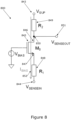
- FIG. 8 shows an example amplifier 800 that can address the second challenge.
- the amplifier 800 comprises a voltage-supply-node (V SUP ) 843, a sense-voltage-input-terminal (V SENSEIN ) 844, and a transistor 845.
- the transistor 845 comprises a first-conduction-channel-terminal 846 connected to the voltage-supply-node 843 and a second-conduction-channel-terminal 847 connected to the sense-voltage-input-node 844.
- the amplifier 800 further comprises a first-resistor (R 1 ) 848 connected in series between the sense-voltage-input-terminal 844 and the second-conduction-channel-terminal 847, a second-resistor (R 2 ) 849 connected in series between the voltage-supply-node 843 and the first-conduction-channel-terminal 846.
- R 1 first-resistor
- R 2 second-resistor
- the amplifier further comprises a sense-node 850 provided between the first-conduction-channel-terminal 846 and the second-resistor 849, and a sense-voltage-output-terminal (V SENSEOUT ) 851 connected to the sense-node 850.
- V SENSEOUT sense-voltage-output-terminal
- FIG. 8 Also shown in Figure 8 is a representation of bias-current, I BIAS , 852, flowing from the voltage-supply-node 843 to the sense-voltage-input-terminal 844.
- the amplifier 800 corresponds to a degenerated common-gate amplifier in which the transistor 845 is an n-type MOSFET, such that the first-conduction-channel-terminal 846 is a drain-terminal and the second-conduction-channel-terminal 847 is a source-terminal.
- an input signal can be applied at the degenerated source-terminal of the transistor 845 instead of at the control-terminal as in a common-source configuration. This allows the input signal to go below ground without any problems.
- the bias-current 852 is also flowing through the sense-voltage-input-terminal 844, which can result in a significant offset if the impedance of the signal source is high.
- a low source impedance e.g. around 50m ⁇ , may address this issue.
- V SENSEOUT V SENSEIN R 2 R 1 ⁇ g m R 1 1 + g m R 1 where g m is the transconductance of the transistor 845.
- a degenerated common-gate amplifier as described above can be used for both lowside sense signals V SENSEPL and V SENSEML to make the first part of the output voltage differential in equation 1.
- V SENSEPH and V SENSEMH a complementary version may be used; i.e., with a p-type MOSFET instead of an n-type MOSFET as the transistor and a bias voltage referring to the supply voltage V SUP instead of ground.
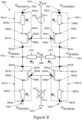
- FIG. 9 shows an example embodiment of a sense amplifier circuit 900 that is based on the example amplifier of Figure 8 .
- the sense amplifier circuit 900 comprises a first-sensed-output-terminal (V SENSEM ) 953, a second-sensed-output-terminal (V SENSEP ) 954, a first-input-voltage-terminal (V SENSEPH ) 955, a second-input-voltage-terminal (V SENSEPL ) 956, a third-input-voltage-terminal (V SENSEMH ) 957, a fourth-input-voltage-terminal (V SENSEML ) 958, and a common-mode-voltage-node (V CM ) 960.
- V SENSEM first-sensed-output-terminal
- V SENSEP second-sensed-output-terminal
- V SENSEPH first-input-voltage-terminal
- V SENSEPL second-
- the sense amplifier circuit 900 allows for a voltage signal at each input-voltage-terminal 955, 956, 957, 958 to be combined into a differential output voltage signal in accordance with equations (1) and (2).
- the sense amplifier circuit 900 may be connected to the output stage of Figure 7 to provide current sensing capability of current flow through the output stage.
- the sense amplifier circuit 900 further comprises first-, second-, third- and fourth-amplification-blocks 961a-d. As shown, each amplification-block 961a-d comprises an amplification-block-input-node 962a-d, an amplification-block-output-node 963a-d and an amplification-block-control-node 964a-d.
- Each amplification-block 961a-d further comprises an amplification-block-transistor 965a-d.
- Each amplification-block-transistor 965a-d comprises a first-conduction-channel-terminal 966a-d, a second-conduction-channel-terminal 967a-d that is connected to the amplification-block-output-node 963a-d, and a control-terminal 968a-d that is connected to the amplification-block-control-node 964a-d.
- An amplification-block-resistor (R 1 ) 969a-d is included in each amplification-block 961a-d and is connected in series between the amplification-block-input-node 962a-d and the first-conduction-channel-terminal 966a-d of the amplification-block-transistor 965a-d.
- the sense amplifier circuit 900 further comprises a first-bias-voltage-source (V BIASH ) 970 connected to the amplification-block-control-nodes 964a, 964c of the first- and third-amplification-blocks 961a, 961c, and a second-bias-voltage-source (V BIASL ) 971 connected to the amplification-block-control-nodes 964b, 964d, of the second- and fourth-amplification-blocks 961b, 961d.
- V BIASH first-bias-voltage-source
- V BIASL second-bias-voltage-source
- the sense amplifier circuit further comprises a first-common-mode-voltage-resistor (R 2 ) 972 connected in series between the first-sensed-output-terminal 953 and the common-mode-voltage-node 960, and a second-common-mode-voltage-resistor (R 2 ) 973 connected in series between the second-sensed-output-terminal 954 and the common-mode-voltage-node 960.
- R 2 first-common-mode-voltage-resistor
- the sense amplifier circuit 900 is further arranged as follows.
- the amplification-block-output-nodes 963a, 963b of the first- and second-amplification-blocks 961a, 961b are connected to the first-sensed-output-terminal 953.
- the amplification-block-output-nodes 963c, 963d of the third- and fourth-amplification-blocks 961c, 961d are connected to the second-sensed-output-terminal 954.
- the amplification-block-input-node 962a of the first-amplification-block 961a is connected to the first-input-voltage-terminal 955.
- the amplification-block-input-node 962b of the second-amplification-block 961b is connected to the second-input-voltage-terminal 956.
- the amplification-block-input-node 962c of the third-amplification-block 961c is connected to the third-input-voltage-terminal 957.
- the amplification-block-input-node 962d of the fourth-amplification-block 961d is connected to the fourth-input-voltage-terminal 958.
- the sense amplifier circuit 900 is configured such that bias currents can flow through the first- and second-amplification-blocks 961a, 961b and through the third- and fourth-amplification-blocks 961c, 961d (i.e., from top to bottom in Figure 7 ).
- a signal current can flow through the first- and second-common-mode-voltage-resistors 972, 973.
- a voltage level at the common-mode-voltage-node 960 which corresponds to a common-mode voltage level of output voltages at the first- and second-sensed-output-terminals 953, 954, can be regulated to any desired level by controlling the voltage level at the first-bias-voltage-source 970 and / or the second-bias-voltage-source 971.
- the sense amplifier circuit 900 can generate a differential output voltage - namely, a voltage at the second-sensed-output-terminal 954 minus a voltage at the first-sensed-output-terminal 953 - that complies with equation (1) and has an additional gain factor given by equation (2).
- the amplification-block-transistor 965a-d is bipolar-junction-transistor, BJT, or a field-effect-transistor, FET, examples of which are described above.
- the amplification-block-transistors 965a, 965c of the first- and third-amplification-blocks 961a, 961c may be p-type metal-oxide-semiconductor FETs, MOSFETs
- the amplification-block-transistors 965b, 965d of the second- and fourth-amplification-blocks 961b, 961b may be n-type MOSFETs.
- the sense amplifier circuit 900 of Figure 9 also comprises a first-reference-voltage-terminal (V SUP ) 974 and a second-reference-voltage-terminal (GND) 975.
- the first-bias-voltage-source (V BIASH ) 970 is connected in series between: (i) the first-reference-voltage-terminal (VSUP) 974, and (ii) the amplification-block-control-nodes 964a, 964c of the first- and third-amplification-blocks 961a, 961c.
- the second-bias-voltage-source (V BIASL ) 971 is connected in series between: (i) the second-reference-voltage-terminal (GND) 975, and (ii) the amplification-block-control-nodes 964b, 964d, of the second- and fourth-amplification-blocks 961b, 961d.
- the sense amplifier circuit 900 shown in Figure 9 provides a solution for how to combine four sense voltages into a single differential voltage.
- both highside (e.g., when the amplification-block-transistors of the first- and third-amplification-blocks are p-type MOSFETs) and lowside (e.g., when the amplification-block-transistors of the second- and fourth-amplification-blocks are n-type MOSFETs) inputs can swing beyond the supply and ground respectively and the highside sense voltages are level-shifted to an appropriate output level without additional circuitry.
- the sense amplifier circuit 900 shown in Figure 9 can be integrated on-chip without the need of external components or additional pins, thereby making it compact.
- the sense amplifier circuit 900 shown in Figure 9 may also allow for measurement of a load current though an output stage, for example the output stage described with respect to Figure 7 , with sufficient accuracy, potentially around 60dB total harmonic distortion, with very limited overhead.
- the sense amplifier circuit 900 may also be power efficient since the bias current from the highside part is shared by the lowside part. Also, because the sense amplifier circuit 900 is essentially a single stage amplifier, all bias currents serve to reduce the equivalent input noise and thus improve the SNR.
- the gain of the sense amplifier depends on the transconductance gm of the transistor, making it temperature and process dependent.
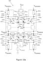
- FIG. 10a shows a further example embodiment of a sense amplifier circuit 1000.
- the sense amplifier circuit is similar to the sense amplifier circuit of Figure 9 in that it comprises first-, second-, third- and fourth-amplification-blocks 1061a-d.
- each amplification-block 1061a-d comprises an amplification-block-control-node 1064a-d, an amplification-block-resistor (R 1 ) 1069a-d, and an amplification-block-transistor 1065a-d comprising a first-conduction-channel-terminal 1066a-d, a second-conduction-channel-terminal 1067a-d, and a control-terminal 1068a-d.
- the sense amplifier circuit 1000 of Figure 10 can be taken to comprise the same features as the sense amplifier circuit of Figure 9 and their corresponding functions.
- connection-node 1076a-d connected in series between the amplification-block-resistor 1069a-d and the first-conduction-channel-terminal 1066a-d, and an amplifier 1077a-d comprising an amplifier-first-input-terminal 1078a-d, an amplifier-second-input-terminal 1079a-d, and an amplifier-output-terminal 1080a-d.
- the amplifier-first-input-terminal 1078a-d is connected to the amplification-block-control-node 1064a-d
- the amplifier-second-input-terminal 1079a-d is connected to the connection-node 1076a-d
- the amplifier-output-terminal 1080a-d is connected to the control-terminal 1068a-d.
- control-terminal 1068a-d is connected indirectly to the amplification-block-control-node 1064a-d through the amplifier 1077a-d.
- each amplification-block 1064a-d may reduce the dependency of gm to temperature and transistor processing. This is because the amplifiers 1077a-d act as gm-boosting feedback loops around the amplification-block-transistors 1065a-d. As a result, the gm of the amplification-block-transistors 1065a-d is multiplied by the gain of the amplifiers 1077a-d in the loop. The effective gm consequently becomes so large that the gain converges to the ratio of the common-mode-voltage-resistors to the amplification-block-resistors (that is, to R 2 /R 1 in equation 2) and so becomes independent on transistor processing and temperature. As such, the noise performance of the sense amplifier circuit is primarily determined by the amplifiers and beneficially is less dependent on the bias current flowing through the sense amplifier circuit core.
- CMOS devices are typically realized using high-voltage (HV) technologies that feature devices capable of handling high voltages, e.g. more than 60V, as well as standard CMOS devices.
- HV high-voltage
- Standard CMOS devices are best suited for signal processing functions because they give the highest gm for a certain current/area budget.
- standard thin-oxide CMOS devices may therefore be appropriate since the input signals are around ground level and the outputs are at low voltage levels in order to match the common-mode input range of a (low-voltage) ADC.
- the highside part of the sense amplifier is essentially a complementary version of the lowside, albeit referring to a supply voltage rather than to ground, so it can also be realized with thin-oxide CMOS. Because the highside outputs refer to ground and not to supply, however, a large voltage difference will appear across the drain and source of the highside PMOS devices.
- Figure 10b shows further features of the sense amplifier circuit 1000 that can address the above problem, features that may be provided in combination with or as an alternative to the features described with reference to Figure 10a .
- the first and third-amplification-blocks 1061a, 1061c comprise an amplification-block-output-node 1063a, 1063c, and amplification-block-cascode-control-node 1081a, 1081c, a transistor 1065a, 1065c comprising a second-conduction-channel-terminal 1067a, 1067c, and a cascode 1082a, 1082c connected in series between the second-conduction-channel-terminal 1067a, 1067c and the amplification-block-output-node 1063a, 1063c.
- the cascodes 1082a, 1082c (which can be high voltage cascodes) can make it possible to isolate the high and low-side circuitry, so they can advantageously be built with smaller devices and process small signals separately at different voltage levels.
- Each cascode 1082a, 1082c comprises a cascode-transistor 1083a, 1083c.
- the cascode-transistor 1083a, 1083c comprises a cascode-transistor-first-conduction-channel-terminal 1084a, 1084c connected to the second-conduction-channel-terminal 1067a, 1067c, a cascode-transistor-second-conduction-channel-terminal 1085a, 1085c connected to the amplification-block-output-node 1063a, 1063c, and a cascode-transistor-control-terminal 1086a, 1086c connected to the amplification-block-cascode-control-node 1081a, 1081c.
- each cascode-transistor 1083a, 1083c is a MOSFET; for example, a p-type MOSFET.
- Each cascode 1082a, 1082c further comprises a cascode-diode 1087a, 1087c comprising a cascode-diode-anode 1088a, 1088c connected to the cascode-transistor-second-conduction-channel-terminal 1085a, 1085c, and a cascode-diode-cathode 1089a, 1089c connected to the cascode-transistor-first-conduction-channel-terminal 1084a, 1084c.
- the sense amplifier circuit 1000 further comprises a first-bias-voltage-source 1070 - compare to the first-bias-voltage-source of the sense amplifier circuit of Figure 9 - and a third-bias-voltage-source (V BIASC ) 1090 connected to the amplification-block-cascode-control-node 1081a, 1081c of the first- and third-amplification-blocks 1061a, 1061c.
- the sense amplifier circuit 1000 comprises a first-reference-voltage-terminal 1074 - compare to the first-reference-voltage-terminal of the sense amplifier circuit of Figure 9 .
- the third-bias-voltage-source 1090 is connected to the first-reference-voltage-terminal 1074.
- each cascode-transistor may be a high-voltage, HV, PMOS transistor.
- the gates of these HV-PMOS transistors are biased with a voltage from the third-bias-voltage-source 1090 that is slightly lower than a voltage from the first-bias-voltage-source 1070 and also refers to the first-reference-voltage-terminal 1074.
- the drain voltages of the PMOS transistors are beneficially shielded from high voltages.
- the outputs of a sense amplifier circuit should match the common-mode input range of a low-voltage ADC for more accurate operation.
- Figure 10c shows further features of the sense amplifier circuit 1000 that can address the above issue, features that may be provided in combination with or as an alternative to the features described with reference to Figures 10a and 10b .
- the sense amplifier circuit 1000 comprises a second-bias-voltage-source (V BIASL ) 1071 comprising a second-bias-voltage-source-output-node 1091 connected to the amplification-block-control-nodes 1064b, 1064d of the second- and fourth-amplification-blocks 1061b, 1061d, a third-bias-voltage-source (V CMREF ) 1092, and a fifth-amplifier 1093.
- V BIASL second-bias-voltage-source
- V CMREF third-bias-voltage-source
- the fifth amplifier 1093 comprises an amplifier-first-input-terminal 1094 connected to the common-mode-voltage-node (V CM ) 1060, an amplifier-second-input-terminal 1095 connected to the third-bias-voltage-source (V CMREF ) 1092, and an amplifier-output-terminal 1096 connected to the second-bias-voltage-source-output-node 1091.
- a common-mode level at the common-mode-voltage-node 1060 can be regulated to a reference voltage level provided by the third-bias-voltage-source 1092 with a common-mode feedback loop provided by the fifth amplifier 1093.
- This loop senses the common-mode level at the common-mode-voltage-node 1060 and compares the common-mode level to the reference voltage level, the output of which corresponds to the output of the second-bias-voltage-source (V BIASL ) 1071.
- the sense amplifier circuit of Figure 9 , 10a , 10b , or 10c is connected to the output stage of Figure 7 .
- each input-voltage-terminal has a corresponding output-stage-amplification-block-sense-terminal.
- the first-input-voltage-terminal is connected to the output-stage-amplification-block-sense-terminal of the first-output-stage-amplification-block
- the second-input-voltage-terminal is connected to the output-stage-amplification-block-sense-terminal of the second-output-stage-amplification-block
- the third-input-voltage-terminal is connected to the output-stage-amplification-block-sense-terminal of the third-output-stage-amplification-block
- the fourth-input-voltage-terminal is connected to the output-stage-amplification-block-sense-terminal of the fourth-output-stage-amplification-block.
- the sense amplifier circuit of Figure 9 , 10a , 10b , or 10c can be connected to any output stage that has an H-bridge mode, such as for a DC Motor.
- the sense amplifier circuit can also be used with segmented power stages.
- the output stage comprises very low-ohmic sense-resistors (such as the sense-resistor 741a-d in Figure 7 ), which can be of the order of 10 m ⁇ , 50 m ⁇ 60 m ⁇ , or 100 m ⁇ , as non-limiting examples. As discussed above, this can be much smaller than the on-resistance of the associated second-output-stage-transistors 734a-d in Figure 7 .
- the on-resistance of the associated second-output-stage-transistors 734a-d may be of the order of 100 m ⁇ , 250m ⁇ , 500 m ⁇ , or 1 ⁇ , as non-limiting examples.
- the ratio between the first- and second-output-stage-transistors can be in the range of 15:1.
- good matching between the sense voltages can be achieved.
- the low impedance of the sense voltages makes them insensitive to disturbances. Consequently, the location of a sense amplifier circuit (e.g., the sense amplifier circuit shown in Figure 10 ) in the floorplan of the output-stage is not critical.
- connection of a sense amplifier circuit as described with reference to Figures 9 and 10a-c to the output-stage of Figure 7 may afford one or more of the advantages set out above.
- any components that are described or illustrated herein as being coupled or connected could be directly or indirectly coupled or galvanically connected. That is, one or more components could be located between two components that are said to be coupled or connected whilst still enabling the required functionality to be achieved.
- the set of instructions/method steps described above are implemented as functional and software instructions embodied as a set of executable instructions which are effected on a computer or machine which is programmed with and controlled by said executable instructions. Such instructions are loaded for execution on a processor (such as one or more CPUs).
- processor includes microprocessors, microcontrollers, processor modules or subsystems (including one or more microprocessors or microcontrollers), or other control or computing devices.
- a processor can refer to a single component or to plural components.
- the set of instructions/methods illustrated herein and data and instructions associated therewith are stored in respective storage devices, which are implemented as one or more non-transient machine or computer-readable or computer-usable storage media or mediums.
- Such computer-readable or computer usable storage medium or media is (are) considered to be part of an article (or article of manufacture).
- An article or article of manufacture can refer to any manufactured single component or multiple components.
- the non-transient machine or computer usable media or mediums as defined herein excludes signals, but such media or mediums may be capable of receiving and processing information from signals and/or other transient mediums.
- Example embodiments of the material discussed in this specification can be implemented in whole or in part through network, computer, or data based devices and/or services. These may include cloud, internet, intranet, mobile, desktop, processor, look-up table, microcontroller, consumer equipment, infrastructure, or other enabling devices and services. As may be used herein and in the claims, the following non-exclusive definitions are provided.
- one or more instructions or steps discussed herein are automated.
- the terms automated or automatically mean controlled operation of an apparatus, system, and/or process using computers and/or mechanical/electrical devices without the necessity of human intervention, observation, effort and/or decision.
- any components said to be coupled may be coupled or connected either directly or indirectly.
- additional components may be located between the two components that are said to be coupled.
Landscapes
- Engineering & Computer Science (AREA)
- Power Engineering (AREA)
- Physics & Mathematics (AREA)
- Multimedia (AREA)
- Acoustics & Sound (AREA)
- Signal Processing (AREA)
- Nonlinear Science (AREA)
- Amplifiers (AREA)
Claims (14)
- Leseverstärkerschaltung (900), die umfasst:einen ersten gelesenen Ausgangsanschluss (953);einen zweiten gelesenen Ausgangsanschluss (954);einen erste Eingangsspannungsanschluss (955);einen zweiten Eingangsspannungsanschluss (956);einen dritten Eingangsspannungsanschluss (957);einen vierten Eingangsspannungsanschluss (958);einen Gleichtakt-Spannungsknoten (960);erste, zweite, dritte und vierte Verstärkungsblöcke (961a-d), wobei jeder Verstärkungsblock (961a-d) umfasst:einen Eingangsknoten des Verstärkungsblocks (962a-d),einen Ausgangsknoten des Verstärkungsblocks (963a-d),einen Steuerknoten des Verstärkungsblocks (964a-d),einen Verstärkungsblocktransistor (965a-d), der umfasst:einen ersten Leitungskanalanschluss (966a-d),einen zweiten Leitungskanalanschluss (967a-d), der mit dem Ausgangsknoten des Verstärkungsblocks (963a-d) verbunden ist, undeinen Steueranschluss (968a-d), der mit dem Steuerknoten des Verstärkungsblocks (964a-d) verbunden ist;einen Verstärkungsblock-Widerstand (969a-d), der zwischen dem Eingangsknoten des Verstärkungsblocks (962a-d) und dem ersten Leitungskanalanschluss (966a-d) in Reihe geschaltet ist,eine erste Vorspannungsquelle (970), die mit den Steuerknoten des Verstärkungsblocks (964a,c) des ersten und dritten Verstärkungsblocks (961a,c) verbunden ist;eine zweite Vorspannungsquelle (971), die mit den Steuerknoten des Verstärkungsblocks (964b,d) des zweiten und vierten Verstärkungsblocks (961b,d) verbunden ist;einen ersten Gleichtaktspannungswiderstand (972), der in Reihe zwischen dem ersten gelesenen Ausgangsanschluss (953) und dem Gleichtaktspannungsknoten (960) geschaltet ist; undeinen zweiten Gleichtaktspannungswiderstand (973), der in Reihe zwischen dem zweiten gelesenen Ausgangsanschluss (954) und dem Gleichtaktspannungsknoten (960) geschaltet ist,wobei:die Ausgangsknoten des Verstärkungsblocks (963a, 963b) des ersten und zweiten Verstärkungsblocks (961a, 961b) mit einem ersten gelesenen Ausgangsanschluss (953) verbunden sind;die Ausgangsknoten des Verstärkungsblocks (963c, 963d) des dritten und vierten Verstärkungsblocks (961c, 961d) mit dem zweiten gelesenen Ausgangsanschluss (954) verbunden sind;der Eingangsknoten des Verstärkungsblocks (962a) des ersten Verstärkungsblocks (961a) mit dem ersten Eingangsspannungsschluss (955) verbunden ist;der Eingangsknoten des Verstärkungsblocks (962b) des zweiten Verstärkungsblocks (961b) mit dem zweiten Eingangsspannungsschluss (956) verbunden ist;der Eingangsknoten des Verstärkungsblocks (962c) des dritten Verstärkungsblocks (961c) mit dem dritten Eingangsspannungsschluss (957) verbunden ist; undder Eingangsknoten des Verstärkungsblocks (962d) des vierten Verstärkungsblocks (961d) mit dem vierten Eingangsspannungsschluss (958) verbunden ist;wobei die ersten und dritten Verstärkungsblocktransistoren Metall-Oxid-Halbleiter-Feldeffekttransistoren, MOSFETs, der p-Art (965a, 965c) und die zweiten und vierten Verstärkungsblocktransistoren MOSFETs der n-Art (965b, 965d) sind.
- Leseverstärkerschaltung (900), die umfasst:einen ersten gelesenen Ausgangsanschluss (953);einen zweiten gelesenen Ausgangsanschluss (954);einen erste Eingangsspannungsanschluss (955);einen zweiten Eingangsspannungsanschluss (956);einen dritten Eingangsspannungsanschluss (957);einen vierten Eingangsspannungsanschluss (958);einen Gleichtakt-Spannungsknoten (960);erste, zweite, dritte und vierte Verstärkungsblöcke (961a-d), wobei jeder Verstärkungsblock (961a-d) umfasst:einen Eingangsknoten des Verstärkungsblocks (962a-d),einen Ausgangsknoten des Verstärkungsblocks (963a-d),einen Steuerknoten des Verstärkungsblocks (964a-d),einen Verstärkungsblocktransistor (965a-d), der umfasst:einen ersten Leitungskanalanschluss (966a-d),einen zweiten Leitungskanalanschluss (967a-d), der mit dem Ausgangsknoten des Verstärkungsblocks (963a-d) verbunden ist, undeinen Steueranschluss (968a-d), der mit dem Steuerknoten des Verstärkungsblocks (964a-d) verbunden ist;einen Verstärkungsblock-Widerstand (969a-d), der zwischen dem Eingangsknoten des Verstärkungsblocks (962a-d) und dem ersten Leitungskanalanschluss (966a-d) in Reihe geschaltet ist,eine erste Vorspannungsquelle (970), die mit den Steuerknoten des Verstärkungsblocks (964a,c) des ersten und dritten Verstärkungsblocks (961a,c) verbunden ist;eine zweite Vorspannungsquelle (971), die mit den Steuerknoten des Verstärkungsblocks (964b,d) des zweiten und vierten Verstärkungsblocks (961b,d) verbunden ist;einen ersten Gleichtaktspannungswiderstand (972), der in Reihe zwischen dem ersten gelesenen Ausgangsanschluss (953) und dem Gleichtaktspannungsknoten (960) geschaltet ist; undeinen zweiten Gleichtaktspannungswiderstand (973), der in Reihe zwischen dem zweiten gelesenen Ausgangsanschluss (954) und dem Gleichtaktspannungsknoten (960) geschaltet ist,wobei:die Ausgangsknoten des Verstärkungsblocks (963a, 963b) des ersten und zweiten Verstärkungsblocks (961a, 961b) mit dem ersten gelesenen Ausgangsanschluss (953) verbunden sind;die Ausgangsknoten des Verstärkungsblocks (963c, 963d) des dritten und vierten Verstärkungsblocks (961c, 961d) mit dem zweiten gelesenen Ausgangsanschluss (954) verbunden sind;der Eingangsknoten des Verstärkungsblocks (962a) des ersten Verstärkungsblocks (961a) mit dem ersten Eingangsspannungsschluss (955) verbunden ist;der Eingangsknoten des Verstärkungsblocks (962b) des zweiten Verstärkungsblocks (961b) mit dem zweiten Eingangsspannungsschluss (956) verbunden ist;der Eingangsknoten des Verstärkungsblocks (962c) des dritten Verstärkungsblocks (961c) mit dem dritten Eingangsspannungsschluss (957) verbunden ist; undder Eingangsknoten des Verstärkungsblocks (962d) des vierten Verstärkungsblocks (961d) mit dem vierten Eingangsspannungsschluss (958) verbunden ist;wobei die ersten und dritten Verstärkungsblocktransistoren Bipolartransistoren, BJTs, der Art pnp (965a, 965c) sind, die zweiten und vierten Verstärkungsblocktransistoren BJTs der Art npn (965b, 965d) sind.
- Leseverstärkerschaltung nach einem der vorhergehenden Ansprüche, die einen ersten Referenzspannungsanschluss (974) umfasst, der mit der ersten Vorspannungsquelle verbunden ist, und einen zweiten Referenzspannungsanschluss (975), der mit der zweiten Vorspannungsquelle verbunden ist.
- Leseverstärkerschaltung nach einem der vorhergehenden Ansprüche, wobei jeder Verstärkungsblock umfasst:einen Verbindungsknoten (1076a-d), der mit dem Verstärkungsblockwiderstand und dem ersten Leitungskanalanschluss verbunden ist;einen Verstärker (1077a-d), der umfasst:einen ersten Eingangsanschluss des Verstärkers(1078a-d);einen zweiten Eingangsanschluss des Verstärkers(1079a-d); undeinen Ausgangsanschluss des Verstärkers (1080a-d);wobei:der erste Eingangsanschluss des Verstärkers mit dem Steuerknoten des Verstärkungsblocks verbunden ist;der zweite Eingangsanschluss des Verstärkers mit dem Verbindungsknoten verbunden ist; undder Ausgangsanschluss des Verstärkers mit dem Steueranschluss verbunden ist, so dass der Steueranschluss über den Verstärker mit dem Steuerknoten des Verstärkungsblocks verbunden ist.
- Leseverstärkerschaltung nach einem der vorhergehenden Ansprüche, wobei die ersten und dritten Verstärkungsblöcke umfassen:einen Kaskodensteuerknoten des Verstärkungsblocks (1081a, 1081c);eine Kaskode (1082a, 1082c), die in Reihe zwischen dem zweiten Leitungskanalanschluss und dem Ausgangsknoten des Verstärkungsblocks geschaltet ist, wobei die Kaskode umfasst:
einen Kaskodentransistor (1083a, 1083c), der umfasst:einen ersten Leitungskanalanschluss des Kaskodentransistors (1084a, 1084c), der mit dem zweiten Leitungskanalanschluss verbunden ist,einen zweiten Leitungskanalanschluss des Kaskodentransistors (1085a, 1085c), der mit dem Ausgangsknoten des Verstärkungsblocks verbunden ist, und einen Steueranschluss des Kaskodentransistors (1086a, 1086c), der mit dem Kaskodensteuerknoten des Verstärkungsblocks verbunden ist, undeine Kaskodendiode (1087a, 1087c), die umfasst:eine Kaskodendiodenanode (1088a, 1088c), die mit dem zweiten Leitungskanalanschluss des Kaskodentransistors verbunden ist, undeine Kaskodendiodenkathode (1089a, 1089c), die mit dem ersten Leitungskanalanschluss des Kaskodentransistors verbunden ist. - Leseverstärkerschaltung nach Anspruch 5, wobei die Leseverstärkerschaltung eine dritte Vorspannungsquelle (1090) umfasst, die mit dem Kaskodensteuerknoten des Verstärkungsblocks des ersten und dritten Verstärkungsblocks verbunden ist.
- Leseverstärkerschaltung nach Anspruch 5 oder Anspruch 6, wobei jeder Kaskodentransistor ein MOSFET der p-Art ist.
- Leseverstärkerschaltung nach Anspruch 6 oder Anspruch 7, wobei die dritte Vorspannungsquelle mit dem ersten Referenzspannungsanschluss verbunden ist.
- Leseverstärkerschaltung nach einem der vorhergehenden Ansprüche, wobei die zweite Vorspannungsquelle umfasst:einen zweiten Vorspannungsquellen-Ausgangsknoten (1091), der mit den Steuerknoten des Verstärkungsblocks des zweiten und vierten Verstärkungsblocks verbunden ist;eine dritte Vorspannungsquelle (1092);einen fünften Verstärker (1093), der umfasst:einen ersten Eingangsanschluss des Verstärkers (1094),der mit dem Gleichtakt-Spannungsknoten verbunden ist;einen zweiten Eingangsanschluss des Verstärkers (1095), der mit der dritten Vorspannungsquelle verbunden ist; undeinen Ausgangsanschluss des Verstärkers (1094), der mit dem zweiten Vorspannungsquellen-Ausgangsknoten verbunden ist.
- Ausgangsstufe (700), die umfasst:die Leseverstärkerschaltung nach einem der vorhergehenden Ansprüche,einen ersten Referenzspannungsanschluss der Ausgangsstufe (702);einen zweiten Referenzspannungsanschluss der Ausgangsstufe (703);einen ersten Ausgangsspannungsanschluss der Ausgangsstufe (704);einen zweiten Ausgangsspannungsanschluss der Ausgangsstufe(705);einen ersten Ausgangsgeräteanschluss (719);einen zweiten Ausgangsgeräteanschluss (720);eine erste Tiefpass-Schaltung (708a), die in Reihe zwischen dem ersten Ausgagnsgeräteanschluss und dem ersten Ausgangsspannungsanschluss der Ausgangsstufe geschaltet ist;eine zweite Tiefpass-Schaltung (708b), die in Reihe zwischen dem zweiten Ausgagnsgeräteanschluss und dem zweiten Ausgangsspannungsanschluss der Ausgangsstufe geschaltet ist;erste, zweite, dritte und vierte Verstärkungsblöcke der Ausgangsstufe (721a-d), wobei jeder Verstärkungsblock der Ausgangsstufe umfasst:einen Eingangsknoten des Verstärkungsblocks der Ausgangsstufe(722a-d),einen Ausgangsknoten des Verstärkungsblocks der Ausgangsstufe (723a-d),einen Verstärkungsblock-Steueranschluss der Ausgangsstufe (724a-d),einen Verstärkungsblock-Leseanschluss der Ausgangsstufe (725a-d),einen ersten Transistor der Ausgangsstufe (727a-d), der umfasst:einen ersten Anschluss des ersten Transistors der Ausgangsstufe (728a-d), der mit dem Eingangsknoten des Verstärkungsblocks der Ausgangsstufe verbunden ist,einen zweiten Anschluss des ersten Transistors der Ausgangsstufe (729a-d), der mit dem Ausgangsknoten des Verstärkungsblocks der Ausgangsstufe verbunden ist, und einen ersten Steueranschluss des Transistors der Ausgangsstufe (730a-d), der mit dem Steueranschluss des Verstärkungsblocks der Ausgangsstufe verbunden ist,eine erste Ausgangsstufendiode (731a-d), die umfasst:eine erste Ausgangsstufen-Diodenanode (732a-d), die mit dem zweiten Anschluss des ersten Transistors der Ausgangsstufe verbunden ist, undeine erste Ausgangsstufen-Diodenkathode (733a-d), die mit dem ersten Anschluss des ersten Transistors der Ausgangsstufe verbunden ist,einen zweiten Transistor der Ausgangsstufe (734a-d), der parallel zu dem ersten Transistor der Ausgangsstufe zwischen dem Eingangsknoten des Verstärkungsblocks der Ausgangsstufe und dem Ausgangsknoten des Verstärkungsblocks der Ausgangsstufe geschaltet ist, wobei der zweite Transistor der Ausgangsstufe umfasst:einen ersten Anschluss des zweiten Transistors der Ausgangsstufe (735a-d), der mit dem Eingangsknoten des Verstärkungsblocks der Ausgangsstufe verbunden ist,einen zweiten Anschluss des zweiten Transistors der Ausgangsstufe (736a-d), der mit dem Ausgangsknoten des Verstärkungsblocks der Ausgangsstufe verbunden ist, und einen zweiten Steueranschluss des Transistors der Ausgangsstufe (737a-d), der mit dem Steueranschluss des Verstärkungsblocks der Ausgangsstufe verbunden ist,eine zweite Ausgangsstufendiode (738a-d), die umfasst:eine zweite Ausgangsstufen-Diodenanode (739a-d), die mit dem zweiten Anschluss des zweiten Transistors der Ausgangsstufe verbunden ist, undeine zweite Ausgangsstufen-Diodenkathode (740a-d), die mit dem ersten Anschluss des zweiten Transistor der Ausgangsstufe verbunden ist,einen Lesewiderstand (741a-d), der verbunden ist zwischen:dem Eingangsknoten des Verstärkungsblocks der Ausgangsstufe und dem ersten Anschluss des zweiten Transistors der Ausgangsstufe, oderzwischen dem Ausgangsknoten des Verstärkungsblocks der Ausgangsstufe und dem zweiten Anschluss des zweiten Transistors der Ausgangsstufe, undeinen Leseknoten (742a-d) in Reihe zwischen dem Lesewiderstand und dem zweiten Transistor der Ausgangsstufe und verbunden mit dem Leseanschluss des Verstärkungsblocks der Ausgangsstufe; undwobei:der Eingangsknoten des Verstärkungsblocks der Ausgangsstufe der ersten und dritten Verstärkungsblöcke der Ausgangsstufe mit dem ersten Referenzspannungsanschluss der Ausgangsstufe verbunden sind;die Ausgangsknoten des Verstärkungsblocks der Ausgangsstufe der zweiten und vierten Verstärkungsblöcke der Ausgangsstufen mit dem zweiten Referenzspannungsanschluss der Ausgangsstufe verbunden sind;der Ausgangsknoten des Verstärkungsblocks der Ausgangsstufe des ersten Verstärkungsblocks der Ausgangsstufe und der Eingangsknoten des Verstärkungsblocks der Ausgangsstufe des zweiten Verstärkungsblocks der Ausgangsstufe mit dem ersten Ausgangsspannungsanschluss der Ausgangsstufe verbunden sind;der Ausgangsknoten des Verstärkungsblocks der Ausgangsstufe des dritten Verstärkungsblocks der Ausgangsstufe und der Ausgangsstufen-Eingangsknoten des Verstärkungsblocks des vierten Verstärkungsblock der Ausgangsstufe mit dem Ausgangsstufen-Zweitausgangs-Spannungsanschluss verbunden sind;der erste Eingangsspannungsanschluss mit dem Leseanschluss des Verstärkungsblocks der Ausgangsstufe des ersten Verstärkungsblocks der Ausgangsstufe verbunden ist;der zweite Eingangsspannungsanschluss mit dem Leseanschluss des Verstärkungsblocks der Ausgangsstufe des Verstärkungsblocks der zweiten Verstärkungsblocks der Ausgangsstufe verbunden ist;der dritte Eingangsspannungsanschluss mit dem Leseanschluss des Verstärkungsblocks der Ausgangsstufe des dritten Verstärkungsblocks der Ausgangsstufe verbunden ist; undder vierte Eingangsspannungsanschluss mit dem Leseanschluss des Verstärkungsblocks der Ausgangsstufe des vierten Verstärkungsblocks der Ausgangsstufe verbunden ist;
- Ausgangsstufe nach Anspruch 10, die einen Lautsprecher (701) umfasst, der mit dem ersten und dem zweiten Ausgangsgeräteanschluss verbunden ist.
- Ausgangsstufe nach Anspruch 10 oder Anspruch 11, wobei der erste Tiefpassfilter und der zweite Tiefpassfilter eine Induktor-Kondensator-Schaltung, LC-Schaltung, umfassen.
- Ausgangsstufe nach einem der Ansprüche 10 bis 12, wobei jeder erste Transistor der Ausgangsstufe und jeder zweite Transistor der Ausgangsstufe ein Feldeffekttransistor, FET, ist.
- Ausgangsstufe nach einem der Ansprüche 10 bis 13, wobei:die ersten Ausgangsstufendioden Bodydioden der ihnen zugeordneten ersten Transistor der Ausgangsstufen sind, und/oderdie zweiten Ausgangsstufendioden Bodydioden der ihnen zugeordneten zweiten Transistor der Ausgangsstufen sind.
Priority Applications (3)
| Application Number | Priority Date | Filing Date | Title |
|---|---|---|---|
| EP20193019.5A EP3961920B1 (de) | 2020-08-27 | 2020-08-27 | Leseverstärkerschaltung |
| US17/392,508 US11671062B2 (en) | 2020-08-27 | 2021-08-03 | Sense amplifier circuit |
| CN202110922193.6A CN114124000A (zh) | 2020-08-27 | 2021-08-11 | 感测放大器电路 |
Applications Claiming Priority (1)
| Application Number | Priority Date | Filing Date | Title |
|---|---|---|---|
| EP20193019.5A EP3961920B1 (de) | 2020-08-27 | 2020-08-27 | Leseverstärkerschaltung |
Publications (2)
| Publication Number | Publication Date |
|---|---|
| EP3961920A1 EP3961920A1 (de) | 2022-03-02 |
| EP3961920B1 true EP3961920B1 (de) | 2024-11-06 |
Family
ID=72266166
Family Applications (1)
| Application Number | Title | Priority Date | Filing Date |
|---|---|---|---|
| EP20193019.5A Active EP3961920B1 (de) | 2020-08-27 | 2020-08-27 | Leseverstärkerschaltung |
Country Status (3)
| Country | Link |
|---|---|
| US (1) | US11671062B2 (de) |
| EP (1) | EP3961920B1 (de) |
| CN (1) | CN114124000A (de) |
Citations (1)
| Publication number | Priority date | Publication date | Assignee | Title |
|---|---|---|---|---|
| EP3179631B1 (de) * | 2015-12-07 | 2019-11-20 | STMicroelectronics Srl | Klasse-d-audioverstärker mit einer schaltung zum lesen eines zugeführten stroms durch den verstärker an den verbraucher und zugehöriges leseverfahren |
Family Cites Families (7)
| Publication number | Priority date | Publication date | Assignee | Title |
|---|---|---|---|---|
| KR100657860B1 (ko) * | 2004-05-17 | 2006-12-14 | 삼성전자주식회사 | 증폭기 및 증폭기의 과전류 검출 방법 |
| EP2284992B1 (de) | 2009-07-15 | 2013-01-02 | Nxp B.V. | Stromerfassung |
| US8963634B2 (en) | 2012-02-28 | 2015-02-24 | Qualcomm Incorporated | Load current sensing |
| US9461589B2 (en) * | 2014-09-03 | 2016-10-04 | Qualcomm Incorporated | Asymmetric H-bridge in a class D power amplifier |
| US9473851B2 (en) * | 2014-12-22 | 2016-10-18 | Qualcomm Incorporated | Speaker protection circuit with improved accuracy |
| US10206037B2 (en) * | 2016-07-06 | 2019-02-12 | Texas Instruments Incorporated | Amplifier speaker drive current sense |
| EP3425795B1 (de) * | 2017-07-03 | 2021-09-01 | Infineon Technologies Austria AG | Klasse-d-audioverstärker mit überlastungsschutzschaltung |
-
2020
- 2020-08-27 EP EP20193019.5A patent/EP3961920B1/de active Active
-
2021
- 2021-08-03 US US17/392,508 patent/US11671062B2/en active Active
- 2021-08-11 CN CN202110922193.6A patent/CN114124000A/zh active Pending
Patent Citations (1)
| Publication number | Priority date | Publication date | Assignee | Title |
|---|---|---|---|---|
| EP3179631B1 (de) * | 2015-12-07 | 2019-11-20 | STMicroelectronics Srl | Klasse-d-audioverstärker mit einer schaltung zum lesen eines zugeführten stroms durch den verstärker an den verbraucher und zugehöriges leseverfahren |
Also Published As
| Publication number | Publication date |
|---|---|
| US20220069782A1 (en) | 2022-03-03 |
| EP3961920A1 (de) | 2022-03-02 |
| CN114124000A (zh) | 2022-03-01 |
| US11671062B2 (en) | 2023-06-06 |
Similar Documents
| Publication | Publication Date | Title |
|---|---|---|
| CN106851474B (zh) | D类音频放大器以及对应的读取方法 | |
| EP3706313B1 (de) | Verbesserte laststromüberwachungsschaltung und verfahren für einen klasse-ab-verstärker | |
| US7944293B2 (en) | Systems and methods for an adaptive bias circuit for a differential power amplifier | |
| US10698007B2 (en) | Load detector | |
| US8902005B2 (en) | Apparatus and method for wide common mode difference | |
| US9479125B2 (en) | Instrumentation amplifier with rail-to-rail input range | |
| US20120182068A1 (en) | Dc offset tracking circuit | |
| US10797661B2 (en) | Capacitive-coupled chopper instrumentation amplifiers and associated methods | |
| WO2016152267A1 (ja) | 増幅器および電子回路 | |
| EP3961920B1 (de) | Leseverstärkerschaltung | |
| US11323084B2 (en) | Linear amplifier | |
| EP4047376B1 (de) | Stromerfassungsschaltung und lastantriebssteuerungsvorrichtung mit dieser schaltung | |
| EP1839389A2 (de) | Differentialverstärkerschaltung und verfahren zur reduzierung wärmebedingter und durch grosse differentialsignale verursachter offsets | |
| Yeom et al. | 0–30 V common mode range, 120 dB CMRR, and 10 nV/noise floor current shunt monitor IC with an embedded ΣΔ modulated digital interface | |
| TWI915867B (zh) | 具負載電流感測之d類放大器及其操作方法 | |
| JP4839572B2 (ja) | 入力回路 | |
| CN120377843A (zh) | 具负载电流感测的d类放大器及其操作方法 | |
| US20240146267A1 (en) | Auto zero techniques for high voltage analog front-end with robust ac common-mode rejection | |
| JP4071146B2 (ja) | バッファ回路 | |
| CN118740067A (zh) | 功率放大电路 | |
| JP2023168757A (ja) | 増幅器、増幅回路、および電流検出装置 |
Legal Events
| Date | Code | Title | Description |
|---|---|---|---|
| PUAI | Public reference made under article 153(3) epc to a published international application that has entered the european phase |
Free format text: ORIGINAL CODE: 0009012 |
|
| STAA | Information on the status of an ep patent application or granted ep patent |
Free format text: STATUS: THE APPLICATION HAS BEEN PUBLISHED |
|
| AK | Designated contracting states |
Kind code of ref document: A1 Designated state(s): AL AT BE BG CH CY CZ DE DK EE ES FI FR GB GR HR HU IE IS IT LI LT LU LV MC MK MT NL NO PL PT RO RS SE SI SK SM TR |
|
| STAA | Information on the status of an ep patent application or granted ep patent |
Free format text: STATUS: REQUEST FOR EXAMINATION WAS MADE |
|
| 17P | Request for examination filed |
Effective date: 20220902 |
|
| RBV | Designated contracting states (corrected) |
Designated state(s): AL AT BE BG CH CY CZ DE DK EE ES FI FR GB GR HR HU IE IS IT LI LT LU LV MC MK MT NL NO PL PT RO RS SE SI SK SM TR |
|
| RIC1 | Information provided on ipc code assigned before grant |
Ipc: H04R 29/00 20060101ALI20240501BHEP Ipc: H03F 3/183 20060101ALI20240501BHEP Ipc: H03F 3/217 20060101ALI20240501BHEP Ipc: H04R 3/00 20060101ALI20240501BHEP Ipc: H03F 1/52 20060101AFI20240501BHEP |
|
| GRAP | Despatch of communication of intention to grant a patent |
Free format text: ORIGINAL CODE: EPIDOSNIGR1 |
|
| STAA | Information on the status of an ep patent application or granted ep patent |
Free format text: STATUS: GRANT OF PATENT IS INTENDED |
|
| INTG | Intention to grant announced |
Effective date: 20240611 |
|
| GRAS | Grant fee paid |
Free format text: ORIGINAL CODE: EPIDOSNIGR3 |
|
| GRAA | (expected) grant |
Free format text: ORIGINAL CODE: 0009210 |
|
| STAA | Information on the status of an ep patent application or granted ep patent |
Free format text: STATUS: THE PATENT HAS BEEN GRANTED |
|
| AK | Designated contracting states |
Kind code of ref document: B1 Designated state(s): AL AT BE BG CH CY CZ DE DK EE ES FI FR GB GR HR HU IE IS IT LI LT LU LV MC MK MT NL NO PL PT RO RS SE SI SK SM TR |
|
| REG | Reference to a national code |
Ref country code: GB Ref legal event code: FG4D |
|
| REG | Reference to a national code |
Ref country code: CH Ref legal event code: EP |
|
| REG | Reference to a national code |
Ref country code: DE Ref legal event code: R096 Ref document number: 602020040698 Country of ref document: DE |
|
| REG | Reference to a national code |
Ref country code: IE Ref legal event code: FG4D |
|
| REG | Reference to a national code |
Ref country code: LT Ref legal event code: MG9D |
|
| REG | Reference to a national code |
Ref country code: NL Ref legal event code: MP Effective date: 20241106 |
|
| PG25 | Lapsed in a contracting state [announced via postgrant information from national office to epo] |
Ref country code: PT Free format text: LAPSE BECAUSE OF FAILURE TO SUBMIT A TRANSLATION OF THE DESCRIPTION OR TO PAY THE FEE WITHIN THE PRESCRIBED TIME-LIMIT Effective date: 20250306 Ref country code: HR Free format text: LAPSE BECAUSE OF FAILURE TO SUBMIT A TRANSLATION OF THE DESCRIPTION OR TO PAY THE FEE WITHIN THE PRESCRIBED TIME-LIMIT Effective date: 20241106 Ref country code: IS Free format text: LAPSE BECAUSE OF FAILURE TO SUBMIT A TRANSLATION OF THE DESCRIPTION OR TO PAY THE FEE WITHIN THE PRESCRIBED TIME-LIMIT Effective date: 20250306 |
|
| PG25 | Lapsed in a contracting state [announced via postgrant information from national office to epo] |
Ref country code: NL Free format text: LAPSE BECAUSE OF FAILURE TO SUBMIT A TRANSLATION OF THE DESCRIPTION OR TO PAY THE FEE WITHIN THE PRESCRIBED TIME-LIMIT Effective date: 20241106 Ref country code: FI Free format text: LAPSE BECAUSE OF FAILURE TO SUBMIT A TRANSLATION OF THE DESCRIPTION OR TO PAY THE FEE WITHIN THE PRESCRIBED TIME-LIMIT Effective date: 20241106 |
|
| REG | Reference to a national code |
Ref country code: AT Ref legal event code: MK05 Ref document number: 1740500 Country of ref document: AT Kind code of ref document: T Effective date: 20241106 |
|
| PG25 | Lapsed in a contracting state [announced via postgrant information from national office to epo] |
Ref country code: BG Free format text: LAPSE BECAUSE OF FAILURE TO SUBMIT A TRANSLATION OF THE DESCRIPTION OR TO PAY THE FEE WITHIN THE PRESCRIBED TIME-LIMIT Effective date: 20241106 |
|
| PG25 | Lapsed in a contracting state [announced via postgrant information from national office to epo] |
Ref country code: ES Free format text: LAPSE BECAUSE OF FAILURE TO SUBMIT A TRANSLATION OF THE DESCRIPTION OR TO PAY THE FEE WITHIN THE PRESCRIBED TIME-LIMIT Effective date: 20241106 |
|
| PG25 | Lapsed in a contracting state [announced via postgrant information from national office to epo] |
Ref country code: NO Free format text: LAPSE BECAUSE OF FAILURE TO SUBMIT A TRANSLATION OF THE DESCRIPTION OR TO PAY THE FEE WITHIN THE PRESCRIBED TIME-LIMIT Effective date: 20250206 |
|
| PG25 | Lapsed in a contracting state [announced via postgrant information from national office to epo] |
Ref country code: LV Free format text: LAPSE BECAUSE OF FAILURE TO SUBMIT A TRANSLATION OF THE DESCRIPTION OR TO PAY THE FEE WITHIN THE PRESCRIBED TIME-LIMIT Effective date: 20241106 Ref country code: GR Free format text: LAPSE BECAUSE OF FAILURE TO SUBMIT A TRANSLATION OF THE DESCRIPTION OR TO PAY THE FEE WITHIN THE PRESCRIBED TIME-LIMIT Effective date: 20250207 Ref country code: AT Free format text: LAPSE BECAUSE OF FAILURE TO SUBMIT A TRANSLATION OF THE DESCRIPTION OR TO PAY THE FEE WITHIN THE PRESCRIBED TIME-LIMIT Effective date: 20241106 |
|
| PG25 | Lapsed in a contracting state [announced via postgrant information from national office to epo] |
Ref country code: PL Free format text: LAPSE BECAUSE OF FAILURE TO SUBMIT A TRANSLATION OF THE DESCRIPTION OR TO PAY THE FEE WITHIN THE PRESCRIBED TIME-LIMIT Effective date: 20241106 |
|
| PG25 | Lapsed in a contracting state [announced via postgrant information from national office to epo] |
Ref country code: RS Free format text: LAPSE BECAUSE OF FAILURE TO SUBMIT A TRANSLATION OF THE DESCRIPTION OR TO PAY THE FEE WITHIN THE PRESCRIBED TIME-LIMIT Effective date: 20250206 |
|
| PG25 | Lapsed in a contracting state [announced via postgrant information from national office to epo] |
Ref country code: SM Free format text: LAPSE BECAUSE OF FAILURE TO SUBMIT A TRANSLATION OF THE DESCRIPTION OR TO PAY THE FEE WITHIN THE PRESCRIBED TIME-LIMIT Effective date: 20241106 |
|
| PG25 | Lapsed in a contracting state [announced via postgrant information from national office to epo] |
Ref country code: DK Free format text: LAPSE BECAUSE OF FAILURE TO SUBMIT A TRANSLATION OF THE DESCRIPTION OR TO PAY THE FEE WITHIN THE PRESCRIBED TIME-LIMIT Effective date: 20241106 |
|
| PG25 | Lapsed in a contracting state [announced via postgrant information from national office to epo] |
Ref country code: EE Free format text: LAPSE BECAUSE OF FAILURE TO SUBMIT A TRANSLATION OF THE DESCRIPTION OR TO PAY THE FEE WITHIN THE PRESCRIBED TIME-LIMIT Effective date: 20241106 |
|
| PG25 | Lapsed in a contracting state [announced via postgrant information from national office to epo] |
Ref country code: RO Free format text: LAPSE BECAUSE OF FAILURE TO SUBMIT A TRANSLATION OF THE DESCRIPTION OR TO PAY THE FEE WITHIN THE PRESCRIBED TIME-LIMIT Effective date: 20241106 |
|
| PG25 | Lapsed in a contracting state [announced via postgrant information from national office to epo] |
Ref country code: SK Free format text: LAPSE BECAUSE OF FAILURE TO SUBMIT A TRANSLATION OF THE DESCRIPTION OR TO PAY THE FEE WITHIN THE PRESCRIBED TIME-LIMIT Effective date: 20241106 |
|
| PG25 | Lapsed in a contracting state [announced via postgrant information from national office to epo] |
Ref country code: CZ Free format text: LAPSE BECAUSE OF FAILURE TO SUBMIT A TRANSLATION OF THE DESCRIPTION OR TO PAY THE FEE WITHIN THE PRESCRIBED TIME-LIMIT Effective date: 20241106 |
|
| PG25 | Lapsed in a contracting state [announced via postgrant information from national office to epo] |
Ref country code: IT Free format text: LAPSE BECAUSE OF FAILURE TO SUBMIT A TRANSLATION OF THE DESCRIPTION OR TO PAY THE FEE WITHIN THE PRESCRIBED TIME-LIMIT Effective date: 20241106 |
|
| P01 | Opt-out of the competence of the unified patent court (upc) registered |
Free format text: CASE NUMBER: APP_29922/2025 Effective date: 20250623 |
|
| REG | Reference to a national code |
Ref country code: DE Ref legal event code: R097 Ref document number: 602020040698 Country of ref document: DE |
|
| PG25 | Lapsed in a contracting state [announced via postgrant information from national office to epo] |
Ref country code: SE Free format text: LAPSE BECAUSE OF FAILURE TO SUBMIT A TRANSLATION OF THE DESCRIPTION OR TO PAY THE FEE WITHIN THE PRESCRIBED TIME-LIMIT Effective date: 20241106 |
|
| PLBE | No opposition filed within time limit |
Free format text: ORIGINAL CODE: 0009261 |
|
| STAA | Information on the status of an ep patent application or granted ep patent |
Free format text: STATUS: NO OPPOSITION FILED WITHIN TIME LIMIT |
|
| PGFP | Annual fee paid to national office [announced via postgrant information from national office to epo] |
Ref country code: DE Payment date: 20250724 Year of fee payment: 6 |
|
| 26N | No opposition filed |
Effective date: 20250807 |
|
| REG | Reference to a national code |
Ref country code: CH Ref legal event code: H13 Free format text: ST27 STATUS EVENT CODE: U-0-0-H10-H13 (AS PROVIDED BY THE NATIONAL OFFICE) Effective date: 20260324 |
|
| PG25 | Lapsed in a contracting state [announced via postgrant information from national office to epo] |
Ref country code: MC Free format text: LAPSE BECAUSE OF FAILURE TO SUBMIT A TRANSLATION OF THE DESCRIPTION OR TO PAY THE FEE WITHIN THE PRESCRIBED TIME-LIMIT Effective date: 20241106 |
|
| PG25 | Lapsed in a contracting state [announced via postgrant information from national office to epo] |
Ref country code: LU Free format text: LAPSE BECAUSE OF NON-PAYMENT OF DUE FEES Effective date: 20250827 |
|
| PG25 | Lapsed in a contracting state [announced via postgrant information from national office to epo] |
Ref country code: CH Free format text: LAPSE BECAUSE OF NON-PAYMENT OF DUE FEES Effective date: 20250831 |