EP3961920A1 - Leseverstärkerschaltung - Google Patents
Leseverstärkerschaltung Download PDFInfo
- Publication number
- EP3961920A1 EP3961920A1 EP20193019.5A EP20193019A EP3961920A1 EP 3961920 A1 EP3961920 A1 EP 3961920A1 EP 20193019 A EP20193019 A EP 20193019A EP 3961920 A1 EP3961920 A1 EP 3961920A1
- Authority
- EP
- European Patent Office
- Prior art keywords
- output
- amplification
- stage
- terminal
- block
- Prior art date
- Legal status (The legal status is an assumption and is not a legal conclusion. Google has not performed a legal analysis and makes no representation as to the accuracy of the status listed.)
- Granted
Links
Images





Classifications
-
- H—ELECTRICITY
- H03—ELECTRONIC CIRCUITRY
- H03F—AMPLIFIERS
- H03F3/00—Amplifiers with only discharge tubes or only semiconductor devices as amplifying elements
- H03F3/181—Low-frequency amplifiers, e.g. audio preamplifiers
- H03F3/183—Low-frequency amplifiers, e.g. audio preamplifiers with semiconductor devices only
-
- H—ELECTRICITY
- H03—ELECTRONIC CIRCUITRY
- H03F—AMPLIFIERS
- H03F3/00—Amplifiers with only discharge tubes or only semiconductor devices as amplifying elements
- H03F3/20—Power amplifiers, e.g. Class B amplifiers, Class C amplifiers
- H03F3/21—Power amplifiers, e.g. Class B amplifiers, Class C amplifiers with semiconductor devices only
- H03F3/217—Class D power amplifiers; Switching amplifiers
- H03F3/2171—Class D power amplifiers; Switching amplifiers with field-effect devices
-
- H—ELECTRICITY
- H03—ELECTRONIC CIRCUITRY
- H03F—AMPLIFIERS
- H03F1/00—Details of amplifiers with only discharge tubes, only semiconductor devices or only unspecified devices as amplifying elements
- H03F1/32—Modifications of amplifiers to reduce non-linear distortion
- H03F1/3205—Modifications of amplifiers to reduce non-linear distortion in field-effect transistor amplifiers
-
- H—ELECTRICITY
- H03—ELECTRONIC CIRCUITRY
- H03F—AMPLIFIERS
- H03F1/00—Details of amplifiers with only discharge tubes, only semiconductor devices or only unspecified devices as amplifying elements
- H03F1/52—Circuit arrangements for protecting such amplifiers
- H03F1/523—Circuit arrangements for protecting such amplifiers for amplifiers using field-effect devices
-
- H—ELECTRICITY
- H03—ELECTRONIC CIRCUITRY
- H03F—AMPLIFIERS
- H03F3/00—Amplifiers with only discharge tubes or only semiconductor devices as amplifying elements
- H03F3/181—Low-frequency amplifiers, e.g. audio preamplifiers
- H03F3/183—Low-frequency amplifiers, e.g. audio preamplifiers with semiconductor devices only
- H03F3/185—Low-frequency amplifiers, e.g. audio preamplifiers with semiconductor devices only with field-effect devices
-
- H—ELECTRICITY
- H03—ELECTRONIC CIRCUITRY
- H03F—AMPLIFIERS
- H03F3/00—Amplifiers with only discharge tubes or only semiconductor devices as amplifying elements
- H03F3/20—Power amplifiers, e.g. Class B amplifiers, Class C amplifiers
- H03F3/21—Power amplifiers, e.g. Class B amplifiers, Class C amplifiers with semiconductor devices only
- H03F3/217—Class D power amplifiers; Switching amplifiers
- H03F3/2173—Class D power amplifiers; Switching amplifiers of the bridge type
-
- H—ELECTRICITY
- H04—ELECTRIC COMMUNICATION TECHNIQUE
- H04R—LOUDSPEAKERS, MICROPHONES, GRAMOPHONE PICK-UPS OR LIKE ACOUSTIC ELECTROMECHANICAL TRANSDUCERS; ELECTRIC HEARING AIDS; PUBLIC ADDRESS SYSTEMS
- H04R3/00—Circuits for transducers
-
- H—ELECTRICITY
- H04—ELECTRIC COMMUNICATION TECHNIQUE
- H04R—LOUDSPEAKERS, MICROPHONES, GRAMOPHONE PICK-UPS OR LIKE ACOUSTIC ELECTROMECHANICAL TRANSDUCERS; ELECTRIC HEARING AIDS; PUBLIC ADDRESS SYSTEMS
- H04R3/00—Circuits for transducers
- H04R3/007—Protection circuits for transducers
-
- H—ELECTRICITY
- H03—ELECTRONIC CIRCUITRY
- H03F—AMPLIFIERS
- H03F2200/00—Indexing scheme relating to amplifiers
- H03F2200/03—Indexing scheme relating to amplifiers the amplifier being designed for audio applications
-
- H—ELECTRICITY
- H03—ELECTRONIC CIRCUITRY
- H03F—AMPLIFIERS
- H03F2200/00—Indexing scheme relating to amplifiers
- H03F2200/351—Pulse width modulation being used in an amplifying circuit
-
- H—ELECTRICITY
- H03—ELECTRONIC CIRCUITRY
- H03F—AMPLIFIERS
- H03F2200/00—Indexing scheme relating to amplifiers
- H03F2200/393—A measuring circuit being coupled to the output of an amplifier
-
- H—ELECTRICITY
- H03—ELECTRONIC CIRCUITRY
- H03F—AMPLIFIERS
- H03F2200/00—Indexing scheme relating to amplifiers
- H03F2200/456—A scaled replica of a transistor being present in an amplifier
-
- H—ELECTRICITY
- H03—ELECTRONIC CIRCUITRY
- H03F—AMPLIFIERS
- H03F2200/00—Indexing scheme relating to amplifiers
- H03F2200/462—Indexing scheme relating to amplifiers the current being sensed
-
- H—ELECTRICITY
- H03—ELECTRONIC CIRCUITRY
- H03F—AMPLIFIERS
- H03F2200/00—Indexing scheme relating to amplifiers
- H03F2200/481—A resistor being used as sensor
-
- H—ELECTRICITY
- H04—ELECTRIC COMMUNICATION TECHNIQUE
- H04R—LOUDSPEAKERS, MICROPHONES, GRAMOPHONE PICK-UPS OR LIKE ACOUSTIC ELECTROMECHANICAL TRANSDUCERS; ELECTRIC HEARING AIDS; PUBLIC ADDRESS SYSTEMS
- H04R29/00—Monitoring arrangements; Testing arrangements
- H04R29/001—Monitoring arrangements; Testing arrangements for loudspeakers
Definitions
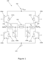
- an audio amplifier such as the output stage shown in Figure 1
- the purpose of an audio amplifier is to force a voltage across a loudspeaker that reproduces an audio input signal with high fidelity. This means that the audio amplifier should not distort the audio input signal. Low distortion is in general achieved by applying feedback.
- a proper feedback loop has high loop gain in the audio frequency range that suppresses nonlinearity of the output stage and, optionally, the first- and second-external-LC-filters.
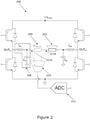
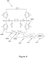
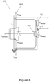
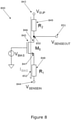
- the amplifier further comprises a sense-node 850 provided between the first-conduction-channel-terminal 846 and the second-resistor 849, and a sense-voltage-output-terminal (V SENSEOUT ) 851 connected to the sense-node 850.
- V SENSEOUT sense-voltage-output-terminal
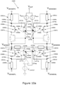
- a common-mode level at the common-mode-voltage-node 1060 can be regulated to a reference voltage level provided by the third-bias-voltage-source 1092 with a common-mode feedback loop provided by the fifth amplifier 1093.
- This loop senses the common-mode level at the common-mode-voltage-node 1060 and compares the common-mode level to the reference voltage level, the output of which corresponds to the output of the second-bias-voltage-source (V BIASL ) 1071.
- the ratio between the first- and second-output-stage-transistors can be in the range of 15:1.
- good matching between the sense voltages can be achieved.
- the low impedance of the sense voltages makes them insensitive to disturbances. Consequently, the location of a sense amplifier circuit (e.g., the sense amplifier circuit shown in Figure 10 ) in the floorplan of the output-stage is not critical.
Landscapes
- Engineering & Computer Science (AREA)
- Power Engineering (AREA)
- Physics & Mathematics (AREA)
- Multimedia (AREA)
- Acoustics & Sound (AREA)
- Signal Processing (AREA)
- Nonlinear Science (AREA)
- Amplifiers (AREA)
Priority Applications (3)
| Application Number | Priority Date | Filing Date | Title |
|---|---|---|---|
| EP20193019.5A EP3961920B1 (de) | 2020-08-27 | 2020-08-27 | Leseverstärkerschaltung |
| US17/392,508 US11671062B2 (en) | 2020-08-27 | 2021-08-03 | Sense amplifier circuit |
| CN202110922193.6A CN114124000A (zh) | 2020-08-27 | 2021-08-11 | 感测放大器电路 |
Applications Claiming Priority (1)
| Application Number | Priority Date | Filing Date | Title |
|---|---|---|---|
| EP20193019.5A EP3961920B1 (de) | 2020-08-27 | 2020-08-27 | Leseverstärkerschaltung |
Publications (2)
| Publication Number | Publication Date |
|---|---|
| EP3961920A1 true EP3961920A1 (de) | 2022-03-02 |
| EP3961920B1 EP3961920B1 (de) | 2024-11-06 |
Family
ID=72266166
Family Applications (1)
| Application Number | Title | Priority Date | Filing Date |
|---|---|---|---|
| EP20193019.5A Active EP3961920B1 (de) | 2020-08-27 | 2020-08-27 | Leseverstärkerschaltung |
Country Status (3)
| Country | Link |
|---|---|
| US (1) | US11671062B2 (de) |
| EP (1) | EP3961920B1 (de) |
| CN (1) | CN114124000A (de) |
Citations (4)
| Publication number | Priority date | Publication date | Assignee | Title |
|---|---|---|---|---|
| US20160065134A1 (en) * | 2014-09-03 | 2016-03-03 | Qualcomm Incorporated | Asymmetric h-bridge in a class d power amplifier |
| US20160182998A1 (en) * | 2014-12-22 | 2016-06-23 | Qualcomm, Incorporated | Speaker protection circuit with improved accuracy |
| EP3179631A1 (de) * | 2015-12-07 | 2017-06-14 | STMicroelectronics Srl | Klasse-d-audioverstärker mit einer schaltung zum lesen eines zugeführten stroms durch den verstärker an den verbraucher und zugehöriges leseverfahren |
| US20180014119A1 (en) * | 2016-07-06 | 2018-01-11 | Texas Instruments Incorporated | Amplifier speaker drive current sense |
Family Cites Families (4)
| Publication number | Priority date | Publication date | Assignee | Title |
|---|---|---|---|---|
| KR100657860B1 (ko) * | 2004-05-17 | 2006-12-14 | 삼성전자주식회사 | 증폭기 및 증폭기의 과전류 검출 방법 |
| EP2284992B1 (de) | 2009-07-15 | 2013-01-02 | Nxp B.V. | Stromerfassung |
| US8963634B2 (en) | 2012-02-28 | 2015-02-24 | Qualcomm Incorporated | Load current sensing |
| EP3425795B1 (de) * | 2017-07-03 | 2021-09-01 | Infineon Technologies Austria AG | Klasse-d-audioverstärker mit überlastungsschutzschaltung |
-
2020
- 2020-08-27 EP EP20193019.5A patent/EP3961920B1/de active Active
-
2021
- 2021-08-03 US US17/392,508 patent/US11671062B2/en active Active
- 2021-08-11 CN CN202110922193.6A patent/CN114124000A/zh active Pending
Patent Citations (4)
| Publication number | Priority date | Publication date | Assignee | Title |
|---|---|---|---|---|
| US20160065134A1 (en) * | 2014-09-03 | 2016-03-03 | Qualcomm Incorporated | Asymmetric h-bridge in a class d power amplifier |
| US20160182998A1 (en) * | 2014-12-22 | 2016-06-23 | Qualcomm, Incorporated | Speaker protection circuit with improved accuracy |
| EP3179631A1 (de) * | 2015-12-07 | 2017-06-14 | STMicroelectronics Srl | Klasse-d-audioverstärker mit einer schaltung zum lesen eines zugeführten stroms durch den verstärker an den verbraucher und zugehöriges leseverfahren |
| US20180014119A1 (en) * | 2016-07-06 | 2018-01-11 | Texas Instruments Incorporated | Amplifier speaker drive current sense |
Non-Patent Citations (3)
| Title |
|---|
| BERKHOUT M: "Integrated Overcurrent Protection System for Class-D Audio Power Amplifiers", IEEE JOURNAL OF SOLID-STATE CIRCUITS, IEEE, USA, vol. 40, no. 11, 2 November 2005 (2005-11-02), pages 2237 - 2245, XP011141632, ISSN: 0018-9200, DOI: 10.1109/JSSC.2005.857369 * |
| FREDERICO CADETE ET AL: "Overcurrent detection circuit for integrated class-D amplifiers", CIRCUIT THEORY AND DESIGN (ECCTD), 2011 20TH EUROPEAN CONFERENCE ON, IEEE, 29 August 2011 (2011-08-29), pages 401 - 404, XP031975566, ISBN: 978-1-4577-0617-2, DOI: 10.1109/ECCTD.2011.6043371 * |
| GUO LINFEI ET AL: "An Ultralow-Power Overcurrent Protection Circuit for Micropower Class D Amplifiers", IEEE TRANSACTIONS ON CIRCUITS AND SYSTEMS II: EXPRESS BRIEFS, IEEE, US, vol. 62, no. 10, 2 October 2015 (2015-10-02), pages 942 - 946, XP011670323, ISSN: 1549-7747, [retrieved on 20150925], DOI: 10.1109/TCSII.2015.2458035 * |
Also Published As
| Publication number | Publication date |
|---|---|
| US20220069782A1 (en) | 2022-03-03 |
| CN114124000A (zh) | 2022-03-01 |
| US11671062B2 (en) | 2023-06-06 |
| EP3961920B1 (de) | 2024-11-06 |
Similar Documents
| Publication | Publication Date | Title |
|---|---|---|
| US7944303B2 (en) | Super source follower output impedance enhancement | |
| US7944293B2 (en) | Systems and methods for an adaptive bias circuit for a differential power amplifier | |
| US8902005B2 (en) | Apparatus and method for wide common mode difference | |
| US10018658B2 (en) | Class D audio amplifier and method for reading a current supplied by the amplifier | |
| US20150077183A1 (en) | Current-feedback operational amplifier | |
| US10944366B2 (en) | Advanced load current monitoring circuit and method for a class-AB amplifier | |
| US9479125B2 (en) | Instrumentation amplifier with rail-to-rail input range | |
| US6313704B1 (en) | Multi-stage signal amplifying circuit | |
| US9379672B2 (en) | Differential current amplifier | |
| US20120182068A1 (en) | Dc offset tracking circuit | |
| US10236878B1 (en) | Isolator device with common-mode voltage regulation | |
| US9461589B2 (en) | Asymmetric H-bridge in a class D power amplifier | |
| WO2016152267A1 (ja) | 増幅器および電子回路 | |
| US9071205B2 (en) | Single input class-AB rail-to-rail output stage | |
| EP3961920B1 (de) | Leseverstärkerschaltung | |
| US11323084B2 (en) | Linear amplifier | |
| US9276468B2 (en) | Low-noise current source | |
| EP3282581B1 (de) | Pufferstufe und steuerschaltung | |
| US20120169421A1 (en) | Audio amplifying circuit with improved noise performance | |
| Yeom et al. | 0–30 V common mode range, 120 dB CMRR, and 10 nV/noise floor current shunt monitor IC with an embedded ΣΔ modulated digital interface | |
| JP4839572B2 (ja) | 入力回路 | |
| US20240146267A1 (en) | Auto zero techniques for high voltage analog front-end with robust ac common-mode rejection | |
| CN120377843A (zh) | 具负载电流感测的d类放大器及其操作方法 | |
| JP4071146B2 (ja) | バッファ回路 | |
| US9431971B2 (en) | Reduced-power dissipation for circuits handling differential pseudo-differential signals |
Legal Events
| Date | Code | Title | Description |
|---|---|---|---|
| PUAI | Public reference made under article 153(3) epc to a published international application that has entered the european phase |
Free format text: ORIGINAL CODE: 0009012 |
|
| STAA | Information on the status of an ep patent application or granted ep patent |
Free format text: STATUS: THE APPLICATION HAS BEEN PUBLISHED |
|
| AK | Designated contracting states |
Kind code of ref document: A1 Designated state(s): AL AT BE BG CH CY CZ DE DK EE ES FI FR GB GR HR HU IE IS IT LI LT LU LV MC MK MT NL NO PL PT RO RS SE SI SK SM TR |
|
| STAA | Information on the status of an ep patent application or granted ep patent |
Free format text: STATUS: REQUEST FOR EXAMINATION WAS MADE |
|
| 17P | Request for examination filed |
Effective date: 20220902 |
|
| RBV | Designated contracting states (corrected) |
Designated state(s): AL AT BE BG CH CY CZ DE DK EE ES FI FR GB GR HR HU IE IS IT LI LT LU LV MC MK MT NL NO PL PT RO RS SE SI SK SM TR |
|
| RIC1 | Information provided on ipc code assigned before grant |
Ipc: H04R 29/00 20060101ALI20240501BHEP Ipc: H03F 3/183 20060101ALI20240501BHEP Ipc: H03F 3/217 20060101ALI20240501BHEP Ipc: H04R 3/00 20060101ALI20240501BHEP Ipc: H03F 1/52 20060101AFI20240501BHEP |
|
| GRAP | Despatch of communication of intention to grant a patent |
Free format text: ORIGINAL CODE: EPIDOSNIGR1 |
|
| STAA | Information on the status of an ep patent application or granted ep patent |
Free format text: STATUS: GRANT OF PATENT IS INTENDED |
|
| INTG | Intention to grant announced |
Effective date: 20240611 |
|
| GRAS | Grant fee paid |
Free format text: ORIGINAL CODE: EPIDOSNIGR3 |
|
| GRAA | (expected) grant |
Free format text: ORIGINAL CODE: 0009210 |
|
| STAA | Information on the status of an ep patent application or granted ep patent |
Free format text: STATUS: THE PATENT HAS BEEN GRANTED |
|
| AK | Designated contracting states |
Kind code of ref document: B1 Designated state(s): AL AT BE BG CH CY CZ DE DK EE ES FI FR GB GR HR HU IE IS IT LI LT LU LV MC MK MT NL NO PL PT RO RS SE SI SK SM TR |
|
| REG | Reference to a national code |
Ref country code: GB Ref legal event code: FG4D |
|
| REG | Reference to a national code |
Ref country code: CH Ref legal event code: EP |
|
| REG | Reference to a national code |
Ref country code: DE Ref legal event code: R096 Ref document number: 602020040698 Country of ref document: DE |
|
| REG | Reference to a national code |
Ref country code: IE Ref legal event code: FG4D |
|
| REG | Reference to a national code |
Ref country code: LT Ref legal event code: MG9D |
|
| REG | Reference to a national code |
Ref country code: NL Ref legal event code: MP Effective date: 20241106 |
|
| PG25 | Lapsed in a contracting state [announced via postgrant information from national office to epo] |
Ref country code: PT Free format text: LAPSE BECAUSE OF FAILURE TO SUBMIT A TRANSLATION OF THE DESCRIPTION OR TO PAY THE FEE WITHIN THE PRESCRIBED TIME-LIMIT Effective date: 20250306 Ref country code: HR Free format text: LAPSE BECAUSE OF FAILURE TO SUBMIT A TRANSLATION OF THE DESCRIPTION OR TO PAY THE FEE WITHIN THE PRESCRIBED TIME-LIMIT Effective date: 20241106 Ref country code: IS Free format text: LAPSE BECAUSE OF FAILURE TO SUBMIT A TRANSLATION OF THE DESCRIPTION OR TO PAY THE FEE WITHIN THE PRESCRIBED TIME-LIMIT Effective date: 20250306 |
|
| PG25 | Lapsed in a contracting state [announced via postgrant information from national office to epo] |
Ref country code: NL Free format text: LAPSE BECAUSE OF FAILURE TO SUBMIT A TRANSLATION OF THE DESCRIPTION OR TO PAY THE FEE WITHIN THE PRESCRIBED TIME-LIMIT Effective date: 20241106 Ref country code: FI Free format text: LAPSE BECAUSE OF FAILURE TO SUBMIT A TRANSLATION OF THE DESCRIPTION OR TO PAY THE FEE WITHIN THE PRESCRIBED TIME-LIMIT Effective date: 20241106 |
|
| REG | Reference to a national code |
Ref country code: AT Ref legal event code: MK05 Ref document number: 1740500 Country of ref document: AT Kind code of ref document: T Effective date: 20241106 |
|
| PG25 | Lapsed in a contracting state [announced via postgrant information from national office to epo] |
Ref country code: BG Free format text: LAPSE BECAUSE OF FAILURE TO SUBMIT A TRANSLATION OF THE DESCRIPTION OR TO PAY THE FEE WITHIN THE PRESCRIBED TIME-LIMIT Effective date: 20241106 |
|
| PG25 | Lapsed in a contracting state [announced via postgrant information from national office to epo] |
Ref country code: ES Free format text: LAPSE BECAUSE OF FAILURE TO SUBMIT A TRANSLATION OF THE DESCRIPTION OR TO PAY THE FEE WITHIN THE PRESCRIBED TIME-LIMIT Effective date: 20241106 |
|
| PG25 | Lapsed in a contracting state [announced via postgrant information from national office to epo] |
Ref country code: NO Free format text: LAPSE BECAUSE OF FAILURE TO SUBMIT A TRANSLATION OF THE DESCRIPTION OR TO PAY THE FEE WITHIN THE PRESCRIBED TIME-LIMIT Effective date: 20250206 |
|
| PG25 | Lapsed in a contracting state [announced via postgrant information from national office to epo] |
Ref country code: LV Free format text: LAPSE BECAUSE OF FAILURE TO SUBMIT A TRANSLATION OF THE DESCRIPTION OR TO PAY THE FEE WITHIN THE PRESCRIBED TIME-LIMIT Effective date: 20241106 Ref country code: GR Free format text: LAPSE BECAUSE OF FAILURE TO SUBMIT A TRANSLATION OF THE DESCRIPTION OR TO PAY THE FEE WITHIN THE PRESCRIBED TIME-LIMIT Effective date: 20250207 Ref country code: AT Free format text: LAPSE BECAUSE OF FAILURE TO SUBMIT A TRANSLATION OF THE DESCRIPTION OR TO PAY THE FEE WITHIN THE PRESCRIBED TIME-LIMIT Effective date: 20241106 |
|
| PG25 | Lapsed in a contracting state [announced via postgrant information from national office to epo] |
Ref country code: PL Free format text: LAPSE BECAUSE OF FAILURE TO SUBMIT A TRANSLATION OF THE DESCRIPTION OR TO PAY THE FEE WITHIN THE PRESCRIBED TIME-LIMIT Effective date: 20241106 |
|
| PG25 | Lapsed in a contracting state [announced via postgrant information from national office to epo] |
Ref country code: RS Free format text: LAPSE BECAUSE OF FAILURE TO SUBMIT A TRANSLATION OF THE DESCRIPTION OR TO PAY THE FEE WITHIN THE PRESCRIBED TIME-LIMIT Effective date: 20250206 |
|
| PG25 | Lapsed in a contracting state [announced via postgrant information from national office to epo] |
Ref country code: SM Free format text: LAPSE BECAUSE OF FAILURE TO SUBMIT A TRANSLATION OF THE DESCRIPTION OR TO PAY THE FEE WITHIN THE PRESCRIBED TIME-LIMIT Effective date: 20241106 |
|
| PG25 | Lapsed in a contracting state [announced via postgrant information from national office to epo] |
Ref country code: DK Free format text: LAPSE BECAUSE OF FAILURE TO SUBMIT A TRANSLATION OF THE DESCRIPTION OR TO PAY THE FEE WITHIN THE PRESCRIBED TIME-LIMIT Effective date: 20241106 |
|
| PG25 | Lapsed in a contracting state [announced via postgrant information from national office to epo] |
Ref country code: EE Free format text: LAPSE BECAUSE OF FAILURE TO SUBMIT A TRANSLATION OF THE DESCRIPTION OR TO PAY THE FEE WITHIN THE PRESCRIBED TIME-LIMIT Effective date: 20241106 |
|
| PG25 | Lapsed in a contracting state [announced via postgrant information from national office to epo] |
Ref country code: RO Free format text: LAPSE BECAUSE OF FAILURE TO SUBMIT A TRANSLATION OF THE DESCRIPTION OR TO PAY THE FEE WITHIN THE PRESCRIBED TIME-LIMIT Effective date: 20241106 |
|
| PG25 | Lapsed in a contracting state [announced via postgrant information from national office to epo] |
Ref country code: SK Free format text: LAPSE BECAUSE OF FAILURE TO SUBMIT A TRANSLATION OF THE DESCRIPTION OR TO PAY THE FEE WITHIN THE PRESCRIBED TIME-LIMIT Effective date: 20241106 |
|
| PG25 | Lapsed in a contracting state [announced via postgrant information from national office to epo] |
Ref country code: CZ Free format text: LAPSE BECAUSE OF FAILURE TO SUBMIT A TRANSLATION OF THE DESCRIPTION OR TO PAY THE FEE WITHIN THE PRESCRIBED TIME-LIMIT Effective date: 20241106 |
|
| PG25 | Lapsed in a contracting state [announced via postgrant information from national office to epo] |
Ref country code: IT Free format text: LAPSE BECAUSE OF FAILURE TO SUBMIT A TRANSLATION OF THE DESCRIPTION OR TO PAY THE FEE WITHIN THE PRESCRIBED TIME-LIMIT Effective date: 20241106 |
|
| P01 | Opt-out of the competence of the unified patent court (upc) registered |
Free format text: CASE NUMBER: APP_29922/2025 Effective date: 20250623 |
|
| REG | Reference to a national code |
Ref country code: DE Ref legal event code: R097 Ref document number: 602020040698 Country of ref document: DE |
|
| PG25 | Lapsed in a contracting state [announced via postgrant information from national office to epo] |
Ref country code: SE Free format text: LAPSE BECAUSE OF FAILURE TO SUBMIT A TRANSLATION OF THE DESCRIPTION OR TO PAY THE FEE WITHIN THE PRESCRIBED TIME-LIMIT Effective date: 20241106 |
|
| PLBE | No opposition filed within time limit |
Free format text: ORIGINAL CODE: 0009261 |
|
| STAA | Information on the status of an ep patent application or granted ep patent |
Free format text: STATUS: NO OPPOSITION FILED WITHIN TIME LIMIT |
|
| PGFP | Annual fee paid to national office [announced via postgrant information from national office to epo] |
Ref country code: DE Payment date: 20250724 Year of fee payment: 6 |
|
| 26N | No opposition filed |
Effective date: 20250807 |
|
| REG | Reference to a national code |
Ref country code: CH Ref legal event code: H13 Free format text: ST27 STATUS EVENT CODE: U-0-0-H10-H13 (AS PROVIDED BY THE NATIONAL OFFICE) Effective date: 20260324 |
|
| PG25 | Lapsed in a contracting state [announced via postgrant information from national office to epo] |
Ref country code: MC Free format text: LAPSE BECAUSE OF FAILURE TO SUBMIT A TRANSLATION OF THE DESCRIPTION OR TO PAY THE FEE WITHIN THE PRESCRIBED TIME-LIMIT Effective date: 20241106 |
|
| PG25 | Lapsed in a contracting state [announced via postgrant information from national office to epo] |
Ref country code: LU Free format text: LAPSE BECAUSE OF NON-PAYMENT OF DUE FEES Effective date: 20250827 |
|
| PG25 | Lapsed in a contracting state [announced via postgrant information from national office to epo] |
Ref country code: CH Free format text: LAPSE BECAUSE OF NON-PAYMENT OF DUE FEES Effective date: 20250831 |