EP3961692A1 - Wiring board, electronic member package, and electronic device - Google Patents
Wiring board, electronic member package, and electronic device Download PDFInfo
- Publication number
- EP3961692A1 EP3961692A1 EP20795036.1A EP20795036A EP3961692A1 EP 3961692 A1 EP3961692 A1 EP 3961692A1 EP 20795036 A EP20795036 A EP 20795036A EP 3961692 A1 EP3961692 A1 EP 3961692A1
- Authority
- EP
- European Patent Office
- Prior art keywords
- base
- lead
- terminal
- wiring board
- joint
- Prior art date
- Legal status (The legal status is an assumption and is not a legal conclusion. Google has not performed a legal analysis and makes no representation as to the accuracy of the status listed.)
- Withdrawn
Links
Images





Classifications
-
- H—ELECTRICITY
- H05—ELECTRIC TECHNIQUES NOT OTHERWISE PROVIDED FOR
- H05K—PRINTED CIRCUITS; CASINGS OR CONSTRUCTIONAL DETAILS OF ELECTRIC APPARATUS; MANUFACTURE OF ASSEMBLAGES OF ELECTRICAL COMPONENTS
- H05K1/00—Printed circuits
- H05K1/02—Details
- H05K1/0213—Electrical arrangements not otherwise provided for
- H05K1/0237—High frequency adaptations
- H05K1/024—Dielectric details, e.g. changing the dielectric material around a transmission line
-
- H—ELECTRICITY
- H10—SEMICONDUCTOR DEVICES; ELECTRIC SOLID-STATE DEVICES NOT OTHERWISE PROVIDED FOR
- H10W—GENERIC PACKAGES, INTERCONNECTIONS, CONNECTORS OR OTHER CONSTRUCTIONAL DETAILS OF DEVICES COVERED BY CLASS H10
- H10W76/00—Containers; Fillings or auxiliary members therefor; Seals
- H10W76/10—Containers or parts thereof
- H10W76/12—Containers or parts thereof characterised by their shape
- H10W76/15—Containers comprising an insulating or insulated base
- H10W76/157—Containers comprising an insulating or insulated base having interconnections parallel to the insulating or insulated base
-
- H—ELECTRICITY
- H10—SEMICONDUCTOR DEVICES; ELECTRIC SOLID-STATE DEVICES NOT OTHERWISE PROVIDED FOR
- H10W—GENERIC PACKAGES, INTERCONNECTIONS, CONNECTORS OR OTHER CONSTRUCTIONAL DETAILS OF DEVICES COVERED BY CLASS H10
- H10W70/00—Package substrates; Interposers; Redistribution layers [RDL]
- H10W70/60—Insulating or insulated package substrates; Interposers; Redistribution layers
- H10W70/62—Insulating or insulated package substrates; Interposers; Redistribution layers characterised by their interconnections
- H10W70/65—Shapes or dispositions of interconnections
-
- H—ELECTRICITY
- H05—ELECTRIC TECHNIQUES NOT OTHERWISE PROVIDED FOR
- H05K—PRINTED CIRCUITS; CASINGS OR CONSTRUCTIONAL DETAILS OF ELECTRIC APPARATUS; MANUFACTURE OF ASSEMBLAGES OF ELECTRICAL COMPONENTS
- H05K1/00—Printed circuits
- H05K1/02—Details
- H05K1/0213—Electrical arrangements not otherwise provided for
- H05K1/0237—High frequency adaptations
- H05K1/0243—Printed circuits associated with mounted high frequency components
-
- H—ELECTRICITY
- H05—ELECTRIC TECHNIQUES NOT OTHERWISE PROVIDED FOR
- H05K—PRINTED CIRCUITS; CASINGS OR CONSTRUCTIONAL DETAILS OF ELECTRIC APPARATUS; MANUFACTURE OF ASSEMBLAGES OF ELECTRICAL COMPONENTS
- H05K1/00—Printed circuits
- H05K1/02—Details
- H05K1/0213—Electrical arrangements not otherwise provided for
- H05K1/0237—High frequency adaptations
- H05K1/0246—Termination of transmission lines
-
- H—ELECTRICITY
- H05—ELECTRIC TECHNIQUES NOT OTHERWISE PROVIDED FOR
- H05K—PRINTED CIRCUITS; CASINGS OR CONSTRUCTIONAL DETAILS OF ELECTRIC APPARATUS; MANUFACTURE OF ASSEMBLAGES OF ELECTRICAL COMPONENTS
- H05K1/00—Printed circuits
- H05K1/02—Details
- H05K1/11—Printed elements for providing electric connections to or between printed circuits
- H05K1/117—Pads along the edge of rigid circuit boards, e.g. for pluggable connectors
-
- H—ELECTRICITY
- H01—ELECTRIC ELEMENTS
- H01R—ELECTRICALLY-CONDUCTIVE CONNECTIONS; STRUCTURAL ASSOCIATIONS OF A PLURALITY OF MUTUALLY-INSULATED ELECTRICAL CONNECTING ELEMENTS; COUPLING DEVICES; CURRENT COLLECTORS
- H01R12/00—Structural associations of a plurality of mutually-insulated electrical connecting elements, specially adapted for printed circuits, e.g. printed circuit boards [PCB], flat or ribbon cables, or like generally planar structures, e.g. terminal strips, terminal blocks; Coupling devices specially adapted for printed circuits, flat or ribbon cables, or like generally planar structures; Terminals specially adapted for contact with, or insertion into, printed circuits, flat or ribbon cables, or like generally planar structures
- H01R12/50—Fixed connections
- H01R12/51—Fixed connections for rigid printed circuits or like structures
- H01R12/55—Fixed connections for rigid printed circuits or like structures characterised by the terminals
- H01R12/57—Fixed connections for rigid printed circuits or like structures characterised by the terminals surface mounting terminals
-
- H—ELECTRICITY
- H01—ELECTRIC ELEMENTS
- H01S—DEVICES USING THE PROCESS OF LIGHT AMPLIFICATION BY STIMULATED EMISSION OF RADIATION [LASER] TO AMPLIFY OR GENERATE LIGHT; DEVICES USING STIMULATED EMISSION OF ELECTROMAGNETIC RADIATION IN WAVE RANGES OTHER THAN OPTICAL
- H01S5/00—Semiconductor lasers
- H01S5/02—Structural details or components not essential to laser action
- H01S5/022—Mountings; Housings
- H01S5/02208—Mountings; Housings characterised by the shape of the housings
-
- H—ELECTRICITY
- H05—ELECTRIC TECHNIQUES NOT OTHERWISE PROVIDED FOR
- H05K—PRINTED CIRCUITS; CASINGS OR CONSTRUCTIONAL DETAILS OF ELECTRIC APPARATUS; MANUFACTURE OF ASSEMBLAGES OF ELECTRICAL COMPONENTS
- H05K1/00—Printed circuits
- H05K1/02—Details
- H05K1/0213—Electrical arrangements not otherwise provided for
- H05K1/0216—Reduction of cross-talk, noise or electromagnetic interference
- H05K1/0218—Reduction of cross-talk, noise or electromagnetic interference by printed shielding conductors, ground planes or power plane
- H05K1/0219—Printed shielding conductors for shielding around or between signal conductors, e.g. coplanar or coaxial printed shielding conductors
-
- H—ELECTRICITY
- H05—ELECTRIC TECHNIQUES NOT OTHERWISE PROVIDED FOR
- H05K—PRINTED CIRCUITS; CASINGS OR CONSTRUCTIONAL DETAILS OF ELECTRIC APPARATUS; MANUFACTURE OF ASSEMBLAGES OF ELECTRICAL COMPONENTS
- H05K1/00—Printed circuits
- H05K1/02—Details
- H05K1/03—Use of materials for the substrate
- H05K1/0306—Inorganic insulating substrates, e.g. ceramic, glass
-
- H—ELECTRICITY
- H05—ELECTRIC TECHNIQUES NOT OTHERWISE PROVIDED FOR
- H05K—PRINTED CIRCUITS; CASINGS OR CONSTRUCTIONAL DETAILS OF ELECTRIC APPARATUS; MANUFACTURE OF ASSEMBLAGES OF ELECTRICAL COMPONENTS
- H05K2201/00—Indexing scheme relating to printed circuits covered by H05K1/00
- H05K2201/09—Shape and layout
- H05K2201/09145—Edge details
- H05K2201/09172—Notches between edge pads
-
- H—ELECTRICITY
- H05—ELECTRIC TECHNIQUES NOT OTHERWISE PROVIDED FOR
- H05K—PRINTED CIRCUITS; CASINGS OR CONSTRUCTIONAL DETAILS OF ELECTRIC APPARATUS; MANUFACTURE OF ASSEMBLAGES OF ELECTRICAL COMPONENTS
- H05K2201/00—Indexing scheme relating to printed circuits covered by H05K1/00
- H05K2201/10—Details of components or other objects attached to or integrated in a printed circuit board
- H05K2201/10227—Other objects, e.g. metallic pieces
- H05K2201/1034—Edge terminals, i.e. separate pieces of metal attached to the edge of the printed circuit board [PCB]
-
- H—ELECTRICITY
- H05—ELECTRIC TECHNIQUES NOT OTHERWISE PROVIDED FOR
- H05K—PRINTED CIRCUITS; CASINGS OR CONSTRUCTIONAL DETAILS OF ELECTRIC APPARATUS; MANUFACTURE OF ASSEMBLAGES OF ELECTRICAL COMPONENTS
- H05K2201/00—Indexing scheme relating to printed circuits covered by H05K1/00
- H05K2201/10—Details of components or other objects attached to or integrated in a printed circuit board
- H05K2201/10613—Details of electrical connections of non-printed components, e.g. special leads
- H05K2201/10742—Details of leads
- H05K2201/10886—Other details
-
- H—ELECTRICITY
- H05—ELECTRIC TECHNIQUES NOT OTHERWISE PROVIDED FOR
- H05K—PRINTED CIRCUITS; CASINGS OR CONSTRUCTIONAL DETAILS OF ELECTRIC APPARATUS; MANUFACTURE OF ASSEMBLAGES OF ELECTRICAL COMPONENTS
- H05K3/00—Apparatus or processes for manufacturing printed circuits
- H05K3/30—Assembling printed circuits with electric components, e.g. with resistors
- H05K3/32—Assembling printed circuits with electric components, e.g. with resistors electrically connecting electric components or wires to printed circuits
- H05K3/34—Assembling printed circuits with electric components, e.g. with resistors electrically connecting electric components or wires to printed circuits by soldering
- H05K3/3405—Edge mounted components, e.g. terminals
Definitions
- the present invention relates to a wiring board, an electronic component package, and an electronic apparatus.
- packages containing semiconductor devices may include lead terminals with tapered ends, or ends gradually thinner toward their tips, for connection to wiring (refer to, for example, Patent Literature 1).
- Patent Literature 1 Japanese Unexamined Patent Application Publication No. 2004-134614
- a wiring board includes a dielectric substrate, a first lead terminal, and a second lead terminal.
- the dielectric substrate has a first surface, a second surface opposite to the first surface, and a first side surface continuous with the first surface and the second surface.
- the first surface includes a first terminal joint and a second terminal joint arranged along the first side surface.
- the first lead terminal includes a first base bonded to the first terminal joint and a first lead extending from the first base.
- the second lead terminal includes a second base bonded to the second terminal joint and a second lead extending from the second base.
- the first base has a larger thickness than the first lead.
- An electronic component package includes a substrate, and the wiring board according to the above aspect bonded to the substrate.
- An electronic apparatus includes the electronic component package according to the above aspect, and an electronic component mounted on the substrate and electrically connected to the wiring board.
- FIG. 1 is a perspective view of a wiring board according to a first embodiment.
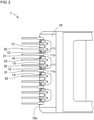
- FIG. 2 is a plan view of the wiring board according to the first embodiment.
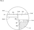
- FIG. 3 is an enlarged cross-sectional view of the wiring board according to the first embodiment.
- FIG. 4 is an enlarged perspective view of the wiring board according to the first embodiment.
- a wiring board 1 includes a dielectric substrate 10, first lead terminals 31, and second lead terminals 32.
- the dielectric substrate 10 has a first surface 10a, a second surface 10b opposite to the first surface 10a, and a first side surface 10c continuous with the first surface 10a and the second surface 10b.
- the dielectric substrate 10 may be a stack of multiple insulating layers formed from a dielectric material.
- the dielectric substrate 10 may be, for example, rectangular, U-shaped, or in any other shape as viewed from above.
- the dielectric material include ceramic materials such as sintered aluminum oxide, sintered mullite, sintered silicon carbide, sintered aluminum nitride, and sintered silicon nitride, or glass ceramic materials.
- the first surface 10a includes one or more first terminal joints 12 and one or more second terminal joints 13 arranged along the first side surface 10c.
- Each first terminal joint 12 is bonded to the corresponding first lead terminal 31 for electrical connection between them.
- Each second terminal joint 13 is bonded to the corresponding second lead terminal 32 for electrical connection between them.
- the first lead terminals 31 are ground terminals
- the second lead terminals 32 are signal terminals.
- the first surface 10a may include multiple first terminal joints 12 and multiple second terminal joints 13 arranged along the first side surface 10c.
- One or more third terminal joints may also be multiple third terminal joints.
- each set of a second terminal joint 13, a first terminal joint 12, and a third terminal joint 14 is arranged repeatedly along the first side surface 10c.
- two first terminal joints 12 may extend away from the first side surface 10c and be connected to each other. This stabilizes the ground potential. The stabilized ground potential improves the frequency response for high-frequency signals.
- Each first terminal joint 12 may include, for example, a metal layer (hereafter, a first metal layer) 12a for electrical connection to the corresponding first lead terminal.
- Each second terminal joint 13 may include, for example, a second metal layer 13a for electrical connection to the corresponding second lead terminal.
- the first metal layers 12a and the second metal layers 13a may be metallization layers formed on the first surface 10a of the dielectric substrate 10.
- the metallization layers are formed from, for example, a metal material such as tungsten, molybdenum, or manganese, and may be plated with nickel or gold.
- the dielectric substrate 10 may include, for example, wiring conductors and conductor layers between the insulating layers.
- the dielectric substrate 10 may include, as viewed from above, multiple wiring conductors and multiple conductor layers overlapping the first metal layers 12a and the second metal layers 13a, which may be electrically connected with feedthrough conductors.
- the wiring conductors and the conductor layers include multiple ground wiring conductors and multiple ground conductor layers that are electrically connected to one another and to the first metal layers 12a.
- the wiring conductors and the conductor layers include multiple signal wiring conductors that are electrically connected to the second metal layers 13a.
- Each first lead terminal 31 is bonded to the corresponding first terminal joint 12 with a bond.
- Each second lead terminal 32 is bonded to the corresponding second terminal joint 13 with a bond.
- the first lead terminals 31 and the second lead terminals 32 are also connected to, for example, an external mounting board.
- the first lead terminals 31 and the second lead terminals 32 may be formed from, for example, a metal material.
- the metal material include iron, copper, nickel, chromium, cobalt, molybdenum or tungsten, or an alloy of these metals, such as a copper-tungsten alloy, a copper-molybdenum alloy, or an iron-nickel-cobalt alloy.
- the bond for bonding the first lead terminals 31 to the first terminal joints 12 and the second lead terminals 32 to the second terminal joints 13 may be, for example, a silver-copper brazing material containing silver and copper as its main components, or a bond with a low melting point (solder) containing silver and copper, and additionally containing tin.
- Each first lead terminal 31 may be bonded to the corresponding first terminal joint 12 by melting the bond on the first terminal joint 12, placing the first lead terminal 31 on the molten bond, and then cooling and solidifying the molten bond.
- Each second lead terminal 32 is connected to the corresponding second terminal joint 13 in the same manner.
- Each first lead terminal 31 includes a first base 31a bonded to the corresponding first terminal joint 12 and a first lead 31b extending from the first base 31a.
- Each second lead terminal 32 includes a second base 32a bonded to the corresponding second terminal joint 13 and a second lead 32b extending from the second base 32a.
- the first lead 31b extends from the first base 31a outwardly from the dielectric substrate 10.
- the second lead 32b extends from the second base 32a outwardly from the dielectric substrate 10.
- Each first lead terminal 31 includes the first base 31a having a larger thickness than the first lead 31b. The thickness herein is the dimension perpendicular to the first surface 10a of the dielectric substrate 10.
- the lead terminals in the wiring board are bonded to the mounting board and can be under an external force.
- the lead terminals being narrow and thin may undergo plastic deformation under an external force and can deviate from being horizontal after mounted.
- the lead terminals being wide and thick can be rigid and may have portions connected with the wiring damaged under an external force and come off together with the wiring. In known wiring boards, such lead terminals can have varying electrical characteristics and thus have deteriorating high-frequency response.
- each first lead terminal 31 includes two portions with different thicknesses, of which the first base 31a bonded to the first terminal joint 12 is thicker.
- the first base 31a that is thicker allows the entire lead terminal to be sufficiently rigid, whereas the first lead 31b that is thinner is flexible and can deform elastically.
- This structure reduces the likelihood of the wiring board 1 being inclined during mounting and allows the wiring board 1 to be closer to being horizontal. This structure thus reduces the likelihood of the wiring board 1 being damaged.
- the lead terminals are less likely to have varying electrical characteristics and improve the high-frequency response of the wiring board 1.
- Each second lead terminal 32 includes the second base 32a and the second lead 32b with the same thickness and the same width. Each second lead terminal 32 is thus entirely band-shaped.
- the second base 32a is a linear portion extending parallel to the first surface 10a and bonded to the second terminal joint 13.
- the second lead 32b includes a bent portion 32b1 that is continuous with the second base 32a and extends away from the dielectric substrate 10 outwardly, and a straight portion 32b2 that is continuous with the bent portion 32b1 and extends parallel to the second base 32a.
- the first base 31a in each first lead terminal 31 may have a larger thickness than the second base 32a in each second lead terminal 32.
- the first base 31a and the first lead 31b may have the same width or may have different widths.
- the first base 31a may have a larger width than the first lead 31b.
- the width herein is the dimension perpendicular to the thickness and to the direction in which the lead extends.
- the first lead 31b is directly bonded to the mounting board. As the width of the first lead 31b is smaller, the wiring on the mounting board can have a smaller width and can be denser.
- the first base 31a contributes to the rigidity of the first lead terminal 31.
- the first base 31a having a smaller width similarly to the first lead 31b can lower the rigidity of the first lead terminal 31.
- the first base 31a thus has a larger width than the first lead 31b to appropriately increase the rigidity of the entire lead terminal.
- the first lead terminals 31 are ground terminals
- the second lead terminals 32 are signal terminals.
- the ground wiring and the signal wiring may both have the same wiring width on the mounting board.
- the first lead 31b and the second lead 32b may have the same width.
- Each second lead terminal 32 includes the second base 32a and the second lead 32b with the same width.
- the first base 31a may have a larger width than the second base 32b.
- the dielectric substrate 10 may have cutouts 11 that are open at the first surface 10a and at the first side surface 10c. Each cutout 11 is located between the first terminal joint 12 and the second terminal joint 13 and defines a space to improve electrical insulation between the first terminal joint 12 and the second terminal joint 13. Also, cutouts similar to the cutouts 11 may be formed between second terminal joints 13.
- the cutouts 11 may have any shape but are rectangular and each have two facing inner surfaces parallel to each other in the present embodiment.
- the cutouts 11 may be, for example, tapered or flared and may each have two facing inner surfaces that are not parallel to each other.
- the dielectric substrate 10 may further include ground conductor layers 11a covering the inner surfaces of the cutouts 11.
- the ground conductor layers 11a may be, for example, metallization layers formed on the inner surfaces of the cutouts 11.
- the metallization layer is formed from, for example, a metal material such as tungsten, molybdenum, or manganese, and may be plated with nickel or gold.
- the ground conductor layers 11a are electrically connected to, for example, the ground wiring conductors, the ground conductor layers, or the first terminal joints 12 (first metal layers 12a) in the dielectric substrate 10 to further stabilize the ground potential.
- each first terminal joint 12 may include a step 20 defined in a portion adjacent to the first side surface 10c and recessed toward the second surface 10b.
- the first terminal joint 12 includes a rectangular portion 20a continuous with the first side surface 10c and located one step (equivalent to, for example, a single insulating layer) closer to the second surface 10b than the other portion.
- the first metal layer 12a is located on the step 20.
- the step 20 includes the rectangular portion 20a and a wall surface 20b between the rectangular portion 20a and the other portion.
- the first metal layer 12a is also located on the wall surface 20b.
- the wall surface 20b increases the area of the first terminal joint 12, or more specifically the first metal layer 12a, in the structure including the step 20 more than in the structure without the step 20. The step 20 thus stabilizes the ground potential further.
- the step 20 is rectangular in the present embodiment, but may be in another polygonal shape or may be semicircular.
- the step 20 with such a shape also has the wall surface that increases the area of the first terminal joint 12, thus stabilizing the ground potential further.
- the first base 31a is either rectangular or prismatic, and the first lead 31b continuous with the end of the first base 31a has a smaller thickness than the first base 31a, is band-shaped, and extends outwardly.
- the first base 31a is bonded to the first terminal joint 12 with a bond.
- the first base 31a overlaps the step 20 as viewed from above.
- the first base 31a may partially overlap the rectangular portion 20a as viewed from above.
- the portion of the first base 31a overlapping the rectangular portion 20a is spaced from the rectangular portion 20a.
- the first base 31a may overlap the step 20 as viewed from above, and may have an end adjacent to the first lead 31b located outwardly from the first side surface 10c.
- the end of the first base 31a opposite to the first lead 31b is bonded to the other portion of the first terminal joint 12 excluding the step 20.
- the first base 31a extends across the rectangular portion 20a as viewed from above, and is firmly bonded to the first terminal joint 12 with the bond entering the entire portion overlapping the rectangular portion 20a.
- the first lead 31b may be connected to the end of the first base 31a at any position in the thickness direction.
- the first lead 31b is connected to the end of the first base 31a at a position most distant from the first terminal joint 12 in the thickness direction.
- the first base 31a has a base first surface 31a1 adjacent to the first terminal joint 12 and a base second surface 31a2 opposite to and parallel to the base first surface 31a1.
- the first lead 31b has a lead first surface 31b1 flush with the base second surface 31a2.
- the first lead 31b has a lead second surface 31b2 parallel to the lead first surface 31b1.
- the lead second surface 31b2 is orthogonal to an end face 31a3 of the first base 31a.
- the end (end face 31a3) of the first base 31a adjacent to the first lead 31b is located outwardly from the first side surface 10c.
- the wiring board 1 may further include third lead terminals 33.
- the first surface 10a of the dielectric substrate 10 includes, opposite to the second terminal joint 13 across each first terminal joint 12, a third terminal joint 14 that is bonded to the third lead terminals 33 with a bond.
- the third lead terminals 33 are signal terminals.
- the first lead terminal 31 as a ground terminal is located between each second lead terminal 32 and the corresponding third lead terminal 33.
- Each third lead terminal 33 includes a third base 33a bonded to the third terminal joint 14 and a third lead 33b extending from the third base 33a.
- the first base 31a has a larger thickness than the third base 33a, similarly to the second base 32a.
- the second lead terminals 32 and the third lead terminals 33 are both signal terminals. When these terminals are electromagnetically coupled to each other, an electrical signal transmitted through one terminal affects an electrical signal transmitted through the other terminal. This noise phenomenon is called crosstalk.
- the second lead 32b and the third lead 33b are weakly coupled to each other electromagnetically with air as the dielectric being between the leads.
- the second base 32a and the third base 33a can be strongly coupled to each other electromagnetically with the dielectric substrate 10 between the bases. Noise from crosstalk is thus more likely to occur between the second base 32a and the third base 33a.
- the first lead terminals 31 are ground terminals.
- the first base 31a of each first lead terminal 31 between the corresponding second base 32a and third base 33a has a larger thickness than the second base 32a and the third base 33a.
- the third base 33a electromagnetically insulates between the second base 32a and the third base 33a, causing the bases to be weakly coupled to each other electromagnetically and thus reducing crosstalk.
- the third lead terminal 33 may have the same shape as or a different shape from the second lead terminal 32.
- the third lead terminals 33 may be formed from the same metal material as or a different material from the second lead terminals 32.
- the third lead terminals 33 and the second lead terminals 32 are formed from the same material and have the same shape.
- FIG. 5 is an enlarged cross-sectional view of a wiring board according to the second embodiment.
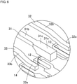
- FIG. 6 is an enlarged perspective view of the wiring board according to the second embodiment.
- the present embodiment is the same as the first embodiment except the structure of the first lead terminals 31.
- the same components as in the first embodiment are given the same reference numerals and will not be described in detail.
- Each first lead terminal 31 includes, between a first base 31a and a first lead 31b, a joint 31c connecting the first base 31a and the first lead 31b.
- the joint 31c has either an inclined surface or a curved surface continuous with one surface of the first base 31a and one surface of the first lead 31b.
- the joint 31c has a curved surface.
- the joint 31c has a joint first surface 31c1 flush with a base second surface 31a2 and a lead first surface 31b1.
- the joint 31c has a joint second surface 31c2 continuous with the base first surface 31a1 of the first base 31a and the lead second surface 31b2 of the first lead 31b.
- the joint second surface 31c2 is a curved surface.
- each first lead terminal 31 may be under an external force applied to the lead first surface 31b1 during bonding to the mounting board, the stress is distributed, thus reducing damage between the first base 31a and the first lead 31b.
- the joint second surface 31c2 may be inclined to produce the same advantageous effects as the curved surface.
- FIG. 7 is an enlarged cross-sectional view of a wiring board according to the third embodiment.
- FIG. 8 is an enlarged perspective view of the wiring board according to the third embodiment.
- the present embodiment is the same as the second embodiment except the structure of the first lead terminals 31.
- the same components as in the second embodiment are given the same reference numerals and will not be described in detail.
- Each first lead terminal 31 in the present embodiment has a recess 310 on a base second surface 31a2 of a first base 31a.
- the recess 310 is a portion of the base second surface 31a2 that is recessed toward the base first surface 31a1.
- the recess 310 may be a portion of the base second surface 31a2 that is cut out from the base first surface 31a1.
- the recess 310 on the base second surface 31a2 lowers the effective relative dielectric constant and improves the high-frequency response.
- the recess 310 in the present embodiment has one end adjacent to the joint 31c located at the boundary between the first base 31a and the joint 31c. This structure reduces a load from the stress applied at the boundary between the first base 31a and the joint 31c.
- the recess 310 in the present embodiment includes an inner wall 310a extending from the boundary between the first base 31a and the joint 31c to its bottom surface.
- the inner wall 310a is inclined with respect to the base first surface 31a1 and with respect to a bottom surface 310b of the recess 310.
- the inner wall 310a may be inclined with respect to the base second surface 31a2. This structure allows the lead terminals to maintain rigidity and reduce a load from the stress applied. This structure thus improves the high-frequency response of the wiring board 1.
- the dielectric substrate 10 including multiple insulating layers formed from, for example, sintered aluminum oxide may be prepared in the manner described below.
- An aluminum oxide-containing powdery raw material and a silicon oxide-containing powdery raw material are mixed with, for example, an appropriate organic binder and an appropriate solvent to form slurry.
- the slurry is then shaped into sheets using, for example, the doctor blade method, to yield multiple ceramic green sheets.
- the ceramic green sheets are then stacked on one another and pressure-bonded.
- the stacked ceramic green sheets are then fired in a reducing atmosphere, and cut or punched into an appropriate shape to complete the dielectric substrate 10 with an intended shape.
- the first metal layers 12a, the second metal layers 13a, the ground conductors, and the signal conductors are formed from, for example, metallization layers that may be formed from a metal having a high melting point, such as tungsten, molybdenum, or manganese, prepared in the manner described below.
- a metal powder with a high melting point is kneaded with an organic solvent and a binder fully into a metal paste.
- the metal paste is then printed at predetermined positions on the ceramic green sheets to be the upper and lower surfaces of the insulating layers by, for example, screen printing. These ceramic green sheets with a printed metal paste are stacked on one another, pressure-bonded, and then co-fired.
- the metallization layer is deposited on the upper surface and the inner layer of the dielectric substrate 10 as the first metal layers 12a, the second metal layers 13a, the ground conductors, and the signal conductors.
- the first metal layer 12a, the second metal layer 13a, and the conductor layers may be plated with nickel or gold.
- the feedthrough conductors are prepared by, for example, forming through-holes in multiple ceramic green sheets to be the insulating layers, and filling the through-holes with a metal paste similar to the metal paste used to form the conductor layers.
- the ceramic green sheets are then stacked on one another, pressure-bonded, and then co-fired to form the feedthrough conductors.
- the through-holes can be formed by, for example, die machining using a metal pin, or punching, for example, with laser.
- the filling of the through-holes with the metal paste may be facilitated with, for example, vacuum suction.
- the first lead terminals 31, the second lead terminals 32, and the third lead terminals 33 may then be prepared by processing (e.g., rolling or punching) an ingot formed from such a metal material.
- the first lead terminals 31, the second lead terminals 32, and the third lead terminals 33 are then bonded to the first terminal joints 12, the second terminal joints 13, and the third terminal joints 14 in the dielectric substrate 10 with a bond to complete the wiring board 1.
- FIG. 9 is a perspective view of an electronic component package and an electronic apparatus according to another embodiment of the present disclosure.
- An electronic component package 50 includes a substrate 2 and the wiring board 1 bonded to the substrate 2.
- the wiring board 1 is U-shaped and is attached to a sidewall 4 to form a frame, which is then bonded to the surface of the substrate 2.
- the substrate 2 and the sidewall 4 may be formed from, for example, a metal such as iron, copper, nickel, chromium, cobalt, molybdenum or tungsten, or an alloy of these metals, such as a copper-tungsten alloy, a copper-molybdenum alloy, or an iron-nickel-cobalt alloy.
- the metal member for the substrate 2 and the sidewall 4 may be prepared by processing (e.g., rolling or punching) an ingot formed from such a metal material.
- An electronic apparatus 100 includes the electronic component package 50, an electronic component 3 mounted on the substrate 2 and electrically connected to the wiring board 1, and a lid 5.
- the electronic component 3 may be, for example, an optical semiconductor device such as a laser diode (LD) or a photodiode (PD).
- the sidewall 4 may have a through-hole 40 to receive an optical fiber.
- the lid 5 is bonded to the upper edges of the wiring board 1, which is a frame, and the sidewall 4 to cover the electronic component package 50.
- the lid 5 may be formed from, for example, a metal such as iron, copper, nickel, chromium, cobalt, molybdenum or tungsten, or an alloy of these metals, such as a copper-tungsten alloy, a copper-molybdenum alloy, or an iron-nickel-cobalt alloy.
- the metal member for the lid 5 may be prepared by processing (e.g., rolling or punching) an ingot formed from such a metal material.
- the electronic component 3 is mounted inside the electronic component package 50, and is electrically connected to the wiring board 1 with, for example, bonding wires. The electronic component 3 is then sealed with the lid 5.
- the present invention is not limited to the above embodiments, and the embodiments may be combined and changed variously without departing from the spirit and scope of the present invention.
- the electronic component package 50 and the electronic apparatus 100 may include the wiring board 1 according to any of the above embodiments or combining any features in the embodiments. Modifications contained in the claims can fall within the scope of the present invention.
Landscapes
- Engineering & Computer Science (AREA)
- Microelectronics & Electronic Packaging (AREA)
- Structure Of Printed Boards (AREA)
- Structures For Mounting Electric Components On Printed Circuit Boards (AREA)
Abstract
Description
- The present invention relates to a wiring board, an electronic component package, and an electronic apparatus.
- As electronic devices including mobile phones are widespread, these devices use electric signals with higher frequencies to transmit larger volumes of information at higher speeds. For better frequency response at high frequencies, packages containing semiconductor devices may include lead terminals with tapered ends, or ends gradually thinner toward their tips, for connection to wiring (refer to, for example, Patent Literature 1).
- Patent Literature 1:
Japanese Unexamined Patent Application Publication No. 2004-134614 - A wiring board according to an aspect of the present disclosure includes a dielectric substrate, a first lead terminal, and a second lead terminal. The dielectric substrate has a first surface, a second surface opposite to the first surface, and a first side surface continuous with the first surface and the second surface. The first surface includes a first terminal joint and a second terminal joint arranged along the first side surface. The first lead terminal includes a first base bonded to the first terminal joint and a first lead extending from the first base. The second lead terminal includes a second base bonded to the second terminal joint and a second lead extending from the second base. The first base has a larger thickness than the first lead.
- An electronic component package according to another aspect of the present disclosure includes a substrate, and the wiring board according to the above aspect bonded to the substrate.
- An electronic apparatus according to still another aspect of the present disclosure includes the electronic component package according to the above aspect, and an electronic component mounted on the substrate and electrically connected to the wiring board.
- The objects, features, and advantages of the present disclosure will become more apparent from the following detailed description and the drawings.
-
FIG. 1 is a perspective view of a wiring board according to a first embodiment. -
FIG. 2 is an enlarged plan view of the wiring board according to the first embodiment. -
FIG. 3 is an enlarged cross-sectional view of the wiring board according to the first embodiment. -
FIG. 4 is an enlarged perspective view of the wiring board according to the first embodiment. -
FIG. 5 is an enlarged cross-sectional view of a wiring board according to a second embodiment. -
FIG. 6 is an enlarged perspective view of the wiring board according to the second embodiment. -
FIG. 7 is an enlarged cross-sectional view of a wiring board according to a third embodiment. -
FIG. 8 is an enlarged perspective view of the wiring board according to the third embodiment. -
FIG. 9 is a perspective view of an electronic component package and an electronic apparatus according to another embodiment. - A wiring board, an electronic component package, and an electronic apparatus according to one or more embodiments of the present disclosure will now be described with reference to the drawings.
FIG. 1 is a perspective view of a wiring board according to a first embodiment.FIG. 2 is a plan view of the wiring board according to the first embodiment.FIG. 3 is an enlarged cross-sectional view of the wiring board according to the first embodiment.FIG. 4 is an enlarged perspective view of the wiring board according to the first embodiment. - The first embodiment of the present disclosure will now be described with reference to
FIGs. 1 to 4 . Awiring board 1 includes adielectric substrate 10,first lead terminals 31, andsecond lead terminals 32. Thedielectric substrate 10 has afirst surface 10a, asecond surface 10b opposite to thefirst surface 10a, and afirst side surface 10c continuous with thefirst surface 10a and thesecond surface 10b. - The
dielectric substrate 10 may be a stack of multiple insulating layers formed from a dielectric material. Thedielectric substrate 10 may be, for example, rectangular, U-shaped, or in any other shape as viewed from above. Examples of the dielectric material include ceramic materials such as sintered aluminum oxide, sintered mullite, sintered silicon carbide, sintered aluminum nitride, and sintered silicon nitride, or glass ceramic materials. - The
first surface 10a includes one or morefirst terminal joints 12 and one or moresecond terminal joints 13 arranged along thefirst side surface 10c. Eachfirst terminal joint 12 is bonded to the correspondingfirst lead terminal 31 for electrical connection between them. Eachsecond terminal joint 13 is bonded to the correspondingsecond lead terminal 32 for electrical connection between them. In the present embodiment, for example, thefirst lead terminals 31 are ground terminals, and thesecond lead terminals 32 are signal terminals. - The
first surface 10a may include multiplefirst terminal joints 12 and multiplesecond terminal joints 13 arranged along thefirst side surface 10c. One or more third terminal joints (described later) may also be multiple third terminal joints. In the present embodiment, for example, each set of asecond terminal joint 13, afirst terminal joint 12, and athird terminal joint 14 is arranged repeatedly along thefirst side surface 10c. In the present embodiment, twofirst terminal joints 12 may extend away from thefirst side surface 10c and be connected to each other. This stabilizes the ground potential. The stabilized ground potential improves the frequency response for high-frequency signals. - Each
first terminal joint 12 may include, for example, a metal layer (hereafter, a first metal layer) 12a for electrical connection to the corresponding first lead terminal. Eachsecond terminal joint 13 may include, for example, asecond metal layer 13a for electrical connection to the corresponding second lead terminal. Thefirst metal layers 12a and thesecond metal layers 13a may be metallization layers formed on thefirst surface 10a of thedielectric substrate 10. The metallization layers are formed from, for example, a metal material such as tungsten, molybdenum, or manganese, and may be plated with nickel or gold. - The
dielectric substrate 10 may include, for example, wiring conductors and conductor layers between the insulating layers. For example, thedielectric substrate 10 may include, as viewed from above, multiple wiring conductors and multiple conductor layers overlapping thefirst metal layers 12a and thesecond metal layers 13a, which may be electrically connected with feedthrough conductors. The wiring conductors and the conductor layers include multiple ground wiring conductors and multiple ground conductor layers that are electrically connected to one another and to thefirst metal layers 12a. The wiring conductors and the conductor layers include multiple signal wiring conductors that are electrically connected to thesecond metal layers 13a. - Each
first lead terminal 31 is bonded to the correspondingfirst terminal joint 12 with a bond. Eachsecond lead terminal 32 is bonded to the correspondingsecond terminal joint 13 with a bond. Thefirst lead terminals 31 and thesecond lead terminals 32 are also connected to, for example, an external mounting board. Thefirst lead terminals 31 and thesecond lead terminals 32 may be formed from, for example, a metal material. Examples of the metal material include iron, copper, nickel, chromium, cobalt, molybdenum or tungsten, or an alloy of these metals, such as a copper-tungsten alloy, a copper-molybdenum alloy, or an iron-nickel-cobalt alloy. - The bond for bonding the
first lead terminals 31 to thefirst terminal joints 12 and thesecond lead terminals 32 to thesecond terminal joints 13 may be, for example, a silver-copper brazing material containing silver and copper as its main components, or a bond with a low melting point (solder) containing silver and copper, and additionally containing tin. Eachfirst lead terminal 31 may be bonded to the correspondingfirst terminal joint 12 by melting the bond on thefirst terminal joint 12, placing thefirst lead terminal 31 on the molten bond, and then cooling and solidifying the molten bond. Eachsecond lead terminal 32 is connected to the correspondingsecond terminal joint 13 in the same manner. - Each
first lead terminal 31 includes afirst base 31a bonded to the corresponding first terminal joint 12 and afirst lead 31b extending from thefirst base 31a. Eachsecond lead terminal 32 includes asecond base 32a bonded to the corresponding second terminal joint 13 and asecond lead 32b extending from thesecond base 32a. Thefirst lead 31b extends from thefirst base 31a outwardly from thedielectric substrate 10. Thesecond lead 32b extends from thesecond base 32a outwardly from thedielectric substrate 10. Eachfirst lead terminal 31 includes thefirst base 31a having a larger thickness than thefirst lead 31b. The thickness herein is the dimension perpendicular to thefirst surface 10a of thedielectric substrate 10. - The lead terminals in the wiring board are bonded to the mounting board and can be under an external force. The lead terminals being narrow and thin may undergo plastic deformation under an external force and can deviate from being horizontal after mounted. The lead terminals being wide and thick can be rigid and may have portions connected with the wiring damaged under an external force and come off together with the wiring. In known wiring boards, such lead terminals can have varying electrical characteristics and thus have deteriorating high-frequency response.
- In the present embodiment, each
first lead terminal 31 includes two portions with different thicknesses, of which thefirst base 31a bonded to the first terminal joint 12 is thicker. Thefirst base 31a that is thicker allows the entire lead terminal to be sufficiently rigid, whereas thefirst lead 31b that is thinner is flexible and can deform elastically. This structure reduces the likelihood of thewiring board 1 being inclined during mounting and allows thewiring board 1 to be closer to being horizontal. This structure thus reduces the likelihood of thewiring board 1 being damaged. The lead terminals are less likely to have varying electrical characteristics and improve the high-frequency response of thewiring board 1. - Each
second lead terminal 32 includes thesecond base 32a and thesecond lead 32b with the same thickness and the same width. Eachsecond lead terminal 32 is thus entirely band-shaped. Thesecond base 32a is a linear portion extending parallel to thefirst surface 10a and bonded to the second terminal joint 13. Thesecond lead 32b includes a bent portion 32b1 that is continuous with thesecond base 32a and extends away from thedielectric substrate 10 outwardly, and a straight portion 32b2 that is continuous with the bent portion 32b1 and extends parallel to thesecond base 32a. Thefirst base 31a in eachfirst lead terminal 31 may have a larger thickness than thesecond base 32a in eachsecond lead terminal 32. - The
first base 31a and thefirst lead 31b may have the same width or may have different widths. In the present embodiment, thefirst base 31a may have a larger width than thefirst lead 31b. The width herein is the dimension perpendicular to the thickness and to the direction in which the lead extends. Thefirst lead 31b is directly bonded to the mounting board. As the width of thefirst lead 31b is smaller, the wiring on the mounting board can have a smaller width and can be denser. Thefirst base 31a contributes to the rigidity of thefirst lead terminal 31. Thefirst base 31a having a smaller width similarly to thefirst lead 31b can lower the rigidity of thefirst lead terminal 31. Thefirst base 31a thus has a larger width than thefirst lead 31b to appropriately increase the rigidity of the entire lead terminal. For example, thefirst lead terminals 31 are ground terminals, and thesecond lead terminals 32 are signal terminals. The ground wiring and the signal wiring may both have the same wiring width on the mounting board. In this case, thefirst lead 31b and thesecond lead 32b may have the same width. Eachsecond lead terminal 32 includes thesecond base 32a and thesecond lead 32b with the same width. Thefirst base 31a may have a larger width than thesecond base 32b. - The
dielectric substrate 10 may havecutouts 11 that are open at thefirst surface 10a and at thefirst side surface 10c. Eachcutout 11 is located between the first terminal joint 12 and the second terminal joint 13 and defines a space to improve electrical insulation between the first terminal joint 12 and the second terminal joint 13. Also, cutouts similar to thecutouts 11 may be formed between second terminal joints 13. - The
cutouts 11 may have any shape but are rectangular and each have two facing inner surfaces parallel to each other in the present embodiment. Thecutouts 11 may be, for example, tapered or flared and may each have two facing inner surfaces that are not parallel to each other. - The
dielectric substrate 10 may further include ground conductor layers 11a covering the inner surfaces of thecutouts 11. Theground conductor layers 11a may be, for example, metallization layers formed on the inner surfaces of thecutouts 11. The metallization layer is formed from, for example, a metal material such as tungsten, molybdenum, or manganese, and may be plated with nickel or gold. The ground conductor layers 11a are electrically connected to, for example, the ground wiring conductors, the ground conductor layers, or the first terminal joints 12 (first metal layers 12a) in thedielectric substrate 10 to further stabilize the ground potential. - In the present embodiment, each first terminal joint 12 may include a
step 20 defined in a portion adjacent to thefirst side surface 10c and recessed toward thesecond surface 10b. For example, the first terminal joint 12 includes arectangular portion 20a continuous with thefirst side surface 10c and located one step (equivalent to, for example, a single insulating layer) closer to thesecond surface 10b than the other portion. Thefirst metal layer 12a is located on thestep 20. Thestep 20 includes therectangular portion 20a and awall surface 20b between therectangular portion 20a and the other portion. Thefirst metal layer 12a is also located on thewall surface 20b. Thewall surface 20b increases the area of the first terminal joint 12, or more specifically thefirst metal layer 12a, in the structure including thestep 20 more than in the structure without thestep 20. Thestep 20 thus stabilizes the ground potential further. - The
step 20 is rectangular in the present embodiment, but may be in another polygonal shape or may be semicircular. Thestep 20 with such a shape also has the wall surface that increases the area of the first terminal joint 12, thus stabilizing the ground potential further. - In the present embodiment, for example, the
first base 31a is either rectangular or prismatic, and thefirst lead 31b continuous with the end of thefirst base 31a has a smaller thickness than thefirst base 31a, is band-shaped, and extends outwardly. As described above, thefirst base 31a is bonded to the first terminal joint 12 with a bond. Thefirst base 31a overlaps thestep 20 as viewed from above. Thefirst base 31a may partially overlap therectangular portion 20a as viewed from above. The portion of thefirst base 31a overlapping therectangular portion 20a is spaced from therectangular portion 20a. When eachfirst lead terminal 31 is connected to the corresponding first terminal joint 12, the molten bond enters the space and solidifies to form a fillet of the bond. This improves the bonding strength between thefirst lead terminal 31 and the first terminal joint 12. - The
first base 31a may overlap thestep 20 as viewed from above, and may have an end adjacent to thefirst lead 31b located outwardly from thefirst side surface 10c. The end of thefirst base 31a opposite to thefirst lead 31b is bonded to the other portion of the first terminal joint 12 excluding thestep 20. Thefirst base 31a extends across therectangular portion 20a as viewed from above, and is firmly bonded to the first terminal joint 12 with the bond entering the entire portion overlapping therectangular portion 20a. - For the connection between the
first base 31a and thefirst lead 31b, thefirst lead 31b may be connected to the end of thefirst base 31a at any position in the thickness direction. In the present embodiment, thefirst lead 31b is connected to the end of thefirst base 31a at a position most distant from the first terminal joint 12 in the thickness direction. More specifically, thefirst base 31a has a base first surface 31a1 adjacent to the first terminal joint 12 and a base second surface 31a2 opposite to and parallel to the base first surface 31a1. Thefirst lead 31b has a lead first surface 31b1 flush with the base second surface 31a2. Thefirst lead 31b has a lead second surface 31b2 parallel to the lead first surface 31b1. The lead second surface 31b2 is orthogonal to an end face 31a3 of thefirst base 31a. In the present embodiment, as shown inFIG. 3 , the end (end face 31a3) of thefirst base 31a adjacent to thefirst lead 31b is located outwardly from thefirst side surface 10c. - In the present embodiment, the
wiring board 1 may further includethird lead terminals 33. Thefirst surface 10a of thedielectric substrate 10 includes, opposite to the second terminal joint 13 across each first terminal joint 12, a third terminal joint 14 that is bonded to thethird lead terminals 33 with a bond. Similarly to thesecond lead terminals 32, thethird lead terminals 33 are signal terminals. Thefirst lead terminal 31 as a ground terminal is located between eachsecond lead terminal 32 and the correspondingthird lead terminal 33. Eachthird lead terminal 33 includes athird base 33a bonded to the third terminal joint 14 and athird lead 33b extending from thethird base 33a. Thefirst base 31a has a larger thickness than thethird base 33a, similarly to thesecond base 32a. - The
second lead terminals 32 and thethird lead terminals 33 are both signal terminals. When these terminals are electromagnetically coupled to each other, an electrical signal transmitted through one terminal affects an electrical signal transmitted through the other terminal. This noise phenomenon is called crosstalk. Thesecond lead 32b and thethird lead 33b are weakly coupled to each other electromagnetically with air as the dielectric being between the leads. In contrast, thesecond base 32a and thethird base 33a can be strongly coupled to each other electromagnetically with thedielectric substrate 10 between the bases. Noise from crosstalk is thus more likely to occur between thesecond base 32a and thethird base 33a. Thefirst lead terminals 31 are ground terminals. Thefirst base 31a of eachfirst lead terminal 31 between the correspondingsecond base 32a andthird base 33a has a larger thickness than thesecond base 32a and thethird base 33a. Thethird base 33a electromagnetically insulates between thesecond base 32a and thethird base 33a, causing the bases to be weakly coupled to each other electromagnetically and thus reducing crosstalk. - The
third lead terminal 33 may have the same shape as or a different shape from thesecond lead terminal 32. Thethird lead terminals 33 may be formed from the same metal material as or a different material from thesecond lead terminals 32. In the present embodiment, thethird lead terminals 33 and thesecond lead terminals 32 are formed from the same material and have the same shape. - A second embodiment will now be described.
FIG. 5 is an enlarged cross-sectional view of a wiring board according to the second embodiment.FIG. 6 is an enlarged perspective view of the wiring board according to the second embodiment. The present embodiment is the same as the first embodiment except the structure of thefirst lead terminals 31. The same components as in the first embodiment are given the same reference numerals and will not be described in detail. - Each
first lead terminal 31 includes, between afirst base 31a and afirst lead 31b, a joint 31c connecting thefirst base 31a and thefirst lead 31b. The joint 31c has either an inclined surface or a curved surface continuous with one surface of thefirst base 31a and one surface of thefirst lead 31b. In the present embodiment, for example, the joint 31c has a curved surface. The joint 31c has a joint first surface 31c1 flush with a base second surface 31a2 and a lead first surface 31b1. The joint 31c has a joint second surface 31c2 continuous with the base first surface 31a1 of thefirst base 31a and the lead second surface 31b2 of thefirst lead 31b. The joint second surface 31c2 is a curved surface. Although eachfirst lead terminal 31 may be under an external force applied to the lead first surface 31b1 during bonding to the mounting board, the stress is distributed, thus reducing damage between thefirst base 31a and thefirst lead 31b. The joint second surface 31c2 may be inclined to produce the same advantageous effects as the curved surface. - A third embodiment will now be described.
FIG. 7 is an enlarged cross-sectional view of a wiring board according to the third embodiment.FIG. 8 is an enlarged perspective view of the wiring board according to the third embodiment. The present embodiment is the same as the second embodiment except the structure of thefirst lead terminals 31. The same components as in the second embodiment are given the same reference numerals and will not be described in detail. - Each
first lead terminal 31 in the present embodiment has arecess 310 on a base second surface 31a2 of afirst base 31a. Therecess 310 is a portion of the base second surface 31a2 that is recessed toward the base first surface 31a1. Therecess 310 may be a portion of the base second surface 31a2 that is cut out from the base first surface 31a1. Therecess 310 on the base second surface 31a2 lowers the effective relative dielectric constant and improves the high-frequency response. - The
recess 310 in the present embodiment has one end adjacent to the joint 31c located at the boundary between thefirst base 31a and the joint 31c. This structure reduces a load from the stress applied at the boundary between thefirst base 31a and the joint 31c. Therecess 310 in the present embodiment includes aninner wall 310a extending from the boundary between thefirst base 31a and the joint 31c to its bottom surface. Theinner wall 310a is inclined with respect to the base first surface 31a1 and with respect to abottom surface 310b of therecess 310. Theinner wall 310a may be inclined with respect to the base second surface 31a2. This structure allows the lead terminals to maintain rigidity and reduce a load from the stress applied. This structure thus improves the high-frequency response of thewiring board 1. - An example method for manufacturing the
wiring board 1 will now be described. Thedielectric substrate 10 including multiple insulating layers formed from, for example, sintered aluminum oxide may be prepared in the manner described below. An aluminum oxide-containing powdery raw material and a silicon oxide-containing powdery raw material are mixed with, for example, an appropriate organic binder and an appropriate solvent to form slurry. The slurry is then shaped into sheets using, for example, the doctor blade method, to yield multiple ceramic green sheets. - The ceramic green sheets are then stacked on one another and pressure-bonded. The stacked ceramic green sheets are then fired in a reducing atmosphere, and cut or punched into an appropriate shape to complete the
dielectric substrate 10 with an intended shape. - The
first metal layers 12a, thesecond metal layers 13a, the ground conductors, and the signal conductors are formed from, for example, metallization layers that may be formed from a metal having a high melting point, such as tungsten, molybdenum, or manganese, prepared in the manner described below. A metal powder with a high melting point is kneaded with an organic solvent and a binder fully into a metal paste. The metal paste is then printed at predetermined positions on the ceramic green sheets to be the upper and lower surfaces of the insulating layers by, for example, screen printing. These ceramic green sheets with a printed metal paste are stacked on one another, pressure-bonded, and then co-fired. Through the above process, the metallization layer is deposited on the upper surface and the inner layer of thedielectric substrate 10 as thefirst metal layers 12a, thesecond metal layers 13a, the ground conductors, and the signal conductors. Thefirst metal layer 12a, thesecond metal layer 13a, and the conductor layers may be plated with nickel or gold. - The feedthrough conductors are prepared by, for example, forming through-holes in multiple ceramic green sheets to be the insulating layers, and filling the through-holes with a metal paste similar to the metal paste used to form the conductor layers. The ceramic green sheets are then stacked on one another, pressure-bonded, and then co-fired to form the feedthrough conductors. The through-holes can be formed by, for example, die machining using a metal pin, or punching, for example, with laser. The filling of the through-holes with the metal paste may be facilitated with, for example, vacuum suction.
- The
first lead terminals 31, thesecond lead terminals 32, and thethird lead terminals 33 may then be prepared by processing (e.g., rolling or punching) an ingot formed from such a metal material. Thefirst lead terminals 31, thesecond lead terminals 32, and thethird lead terminals 33 are then bonded to the firstterminal joints 12, the second terminal joints 13, and the thirdterminal joints 14 in thedielectric substrate 10 with a bond to complete thewiring board 1. -
FIG. 9 is a perspective view of an electronic component package and an electronic apparatus according to another embodiment of the present disclosure. Anelectronic component package 50 includes asubstrate 2 and thewiring board 1 bonded to thesubstrate 2. In the present embodiment, thewiring board 1 is U-shaped and is attached to asidewall 4 to form a frame, which is then bonded to the surface of thesubstrate 2. Thesubstrate 2 and thesidewall 4 may be formed from, for example, a metal such as iron, copper, nickel, chromium, cobalt, molybdenum or tungsten, or an alloy of these metals, such as a copper-tungsten alloy, a copper-molybdenum alloy, or an iron-nickel-cobalt alloy. The metal member for thesubstrate 2 and thesidewall 4 may be prepared by processing (e.g., rolling or punching) an ingot formed from such a metal material. - An
electronic apparatus 100 includes theelectronic component package 50, anelectronic component 3 mounted on thesubstrate 2 and electrically connected to thewiring board 1, and a lid 5. - The
electronic component 3 may be, for example, an optical semiconductor device such as a laser diode (LD) or a photodiode (PD). For an LD, thesidewall 4 may have a through-hole 40 to receive an optical fiber. The lid 5 is bonded to the upper edges of thewiring board 1, which is a frame, and thesidewall 4 to cover theelectronic component package 50. The lid 5 may be formed from, for example, a metal such as iron, copper, nickel, chromium, cobalt, molybdenum or tungsten, or an alloy of these metals, such as a copper-tungsten alloy, a copper-molybdenum alloy, or an iron-nickel-cobalt alloy. The metal member for the lid 5 may be prepared by processing (e.g., rolling or punching) an ingot formed from such a metal material. - The
electronic component 3 is mounted inside theelectronic component package 50, and is electrically connected to thewiring board 1 with, for example, bonding wires. Theelectronic component 3 is then sealed with the lid 5. - The present invention is not limited to the above embodiments, and the embodiments may be combined and changed variously without departing from the spirit and scope of the present invention. For example, the
electronic component package 50 and theelectronic apparatus 100 may include thewiring board 1 according to any of the above embodiments or combining any features in the embodiments. Modifications contained in the claims can fall within the scope of the present invention. -
- 1
- wiring board
- 2
- substrate
- 3
- electronic component
- 4
- sidewall
- 5
- lid
- 10
- dielectric substrate
- 10a
- first surface
- 10b
- second surface
- 10c
- first side surface
- 11
- cutout
- 12
- first terminal joint
- 12a
- first metal layer
- 13
- second terminal joint
- 13a
- second metal layer
- 14
- third terminal joint
- 20
- step
- 20a
- rectangular portion
- 20b
- wall surface
- 31
- first lead terminal
- 31a
- first base
- 31a1
- base first surface
- 31a2
- base second surface
- 31a3
- end face
- 31b
- first lead
- 31b1
- lead first surface
- 31b2
- lead second surface
- 31c
- joint
- 31c1
- joint first surface
- 31c2
- joint second surface
- 32
- second lead terminal
- 32a
- second base
- 32b
- second lead
- 32b1
- bent portion
- 32b2
- straight portion
- 33
- third lead terminal
- 33a
- third base
- 33b
- third lead
- 40
- through-hole
- 50
- electronic component package
- 100
- electronic apparatus
- 310
- recess
- 310a
- inner wall
- 310b
- bottom surface
Claims (16)
- A wiring board, comprising:a dielectric substrate;a first lead terminal; anda second lead terminal,wherein the dielectric substrate has a first surface, a second surface opposite to the first surface, and a first side surface continuous with the first surface and the second surface,the first surface includes a first terminal joint and a second terminal joint arranged along the first side surface,the first lead terminal includes a first base bonded to the first terminal joint and a first lead extending from the first base,the second lead terminal includes a second base bonded to the second terminal joint and a second lead extending from the second base, andthe first base has a larger thickness than the first lead.
- The wiring board according to claim 1, wherein
the first base has a larger thickness than the second base. - The wiring board according to claim 1 or claim 2, wherein
the first base has a larger width than the first lead. - The wiring board according to claim 3, wherein
the first base has a larger width than the second base. - The wiring board according to any one of claims 1 to 4, wherein
the first base has a base first surface adjacent to the first terminal joint and a base second surface parallel to the base first surface, and
the first lead has a lead first surface flush with the base second surface. - The wiring board according to any one of claims 1 to 5, wherein
the first terminal joint includes a step defined in a portion of the first side surface and recessed toward the second surface, and
the first base overlaps the step as viewed from above. - The wiring board according to claim 6, wherein
the first base includes an end adjacent to the first lead and located outward from the first side surface as viewed from above. - The wiring board according to any one of claims 1 to 7, wherein
the first lead terminal further includes a joint between the first base and the first lead, and the joint has an inclined surface or a curved surface continuous with a surface of the first base and a surface of the first lead. - The wiring board according to claim 5 or to any one of claims 6 to 8 dependent from claim 5, wherein
the first base includes a recess on the base second surface. - The wiring board according to claim 9 dependent from claim 8, wherein
the recess includes an end located at a boundary between the first base and the joint. - The wiring board according to claim 9 or claim 10, wherein
the recess includes an inner wall adjacent to a boundary between the first base and the joint,
and
the inner wall is inclined with respect to the base first surface. - The wiring board according to any one of claims 1 to 11, wherein
the first lead terminal is a ground terminal. - The wiring board according to claim 12, further comprising:a third lead terminal,wherein the second lead terminal and the third lead terminal are signal terminals,the first surface includes a third terminal joint located opposite to the second terminal joint across the first terminal joint,the third lead terminal includes a third base bonded to the third terminal joint and a third lead extending from the third base, andthe first base has a larger thickness than the third base.
- The wiring board according to any one of claims 1 to 13, wherein
the dielectric substrate includes
a cutout open at the first surface and the first side surface and located between the first terminal joint and the second terminal joint, and
a conductor layer located on an inner surface of the cutout and continuous with the first terminal joint. - An electronic component package, comprising:a substrate; andthe wiring board according to any one of claims 1 to 14 bonded to the substrate.
- An electronic apparatus, comprising:the electronic component package according to claim 15; andan electronic component mounted on the substrate and electrically connected to the wiring board.
Applications Claiming Priority (2)
| Application Number | Priority Date | Filing Date | Title |
|---|---|---|---|
| JP2019084011 | 2019-04-25 | ||
| PCT/JP2020/017957 WO2020218608A1 (en) | 2019-04-25 | 2020-04-27 | Wiring board, electronic member package, and electronic device |
Publications (2)
| Publication Number | Publication Date |
|---|---|
| EP3961692A1 true EP3961692A1 (en) | 2022-03-02 |
| EP3961692A4 EP3961692A4 (en) | 2023-05-24 |
Family
ID=72942663
Family Applications (1)
| Application Number | Title | Priority Date | Filing Date |
|---|---|---|---|
| EP20795036.1A Withdrawn EP3961692A4 (en) | 2019-04-25 | 2020-04-27 | WIRING BOARD, ELECTRONIC ELEMENT BOX AND ELECTRONIC DEVICE |
Country Status (5)
| Country | Link |
|---|---|
| US (1) | US11889618B2 (en) |
| EP (1) | EP3961692A4 (en) |
| JP (1) | JP7244630B2 (en) |
| CN (1) | CN113748505A (en) |
| WO (1) | WO2020218608A1 (en) |
Family Cites Families (23)
| Publication number | Priority date | Publication date | Assignee | Title |
|---|---|---|---|---|
| JPH04130760A (en) | 1990-09-21 | 1992-05-01 | Matsushita Electric Works Ltd | Semiconductor chip carrier |
| JPH04130761A (en) * | 1990-09-21 | 1992-05-01 | Matsushita Electric Works Ltd | External connection terminal for semiconductor chip carrier |
| US5736784A (en) * | 1996-10-31 | 1998-04-07 | Hewlett-Packard Co. | Variable-width lead interconnection structure and method |
| EP0899795A3 (en) * | 1997-08-27 | 1999-05-12 | Sumitomo Electric Industries, Ltd. | Optical-semiconductor container or module |
| JP2000188366A (en) * | 1998-12-24 | 2000-07-04 | Hitachi Ltd | Semiconductor device |
| CN1258252C (en) * | 2000-07-17 | 2006-05-31 | 三洋电机株式会社 | semiconductor laser device |
| US6381066B1 (en) * | 2000-09-28 | 2002-04-30 | Axsun Technologies, Inc. | Integrated semiconductor optical amplifier system |
| JP2004134614A (en) | 2002-10-11 | 2004-04-30 | Kyocera Corp | Semiconductor element storage package and semiconductor device |
| DE102005036266A1 (en) * | 2005-07-11 | 2007-01-25 | Osram Opto Semiconductors Gmbh | Housing for a laser diode device, laser diode device and method of manufacturing a laser diode device |
| JP2010103456A (en) * | 2008-06-26 | 2010-05-06 | Kyocera Corp | Package for storing image sensor, and image capturing apparatus |
| JP2010153763A (en) * | 2008-08-27 | 2010-07-08 | Kyocera Corp | Package for storing imaging element and imaging device |
| JP5769474B2 (en) | 2011-04-06 | 2015-08-26 | 京セラ株式会社 | Terminal structure, electronic component storage package and electronic device |
| JP6121692B2 (en) * | 2012-11-05 | 2017-04-26 | ルネサスエレクトロニクス株式会社 | Semiconductor device and manufacturing method thereof |
| JP6162800B2 (en) | 2013-05-29 | 2017-07-12 | 京セラ株式会社 | Device storage package and mounting structure |
| JP6193510B2 (en) * | 2014-11-27 | 2017-09-06 | 新電元工業株式会社 | Lead frame, semiconductor device, lead frame manufacturing method, and semiconductor device manufacturing method |
| JP2016146439A (en) | 2015-02-09 | 2016-08-12 | Ngkエレクトロデバイス株式会社 | Package for housing high frequency semiconductor element |
| US10615155B2 (en) * | 2015-03-23 | 2020-04-07 | Gd Midea Airconditioning Equipment Co., Ltd. | Intelligent power module and manufacturing method thereof |
| WO2016186128A1 (en) | 2015-05-20 | 2016-11-24 | 京セラ株式会社 | Semiconductor element package, semiconductor device, and mounting structure |
| US10432152B2 (en) * | 2015-05-22 | 2019-10-01 | Nxp Usa, Inc. | RF amplifier output circuit device with integrated current path, and methods of manufacture thereof |
| US10553523B2 (en) * | 2015-11-20 | 2020-02-04 | Shindengen Electric Manufacturing Co., Ltd. | Semiconductor device |
| JP6622649B2 (en) * | 2015-12-21 | 2019-12-18 | ホシデン株式会社 | Non-contact communication module |
| EP3477693A4 (en) | 2016-06-27 | 2019-06-12 | NGK Electronics Devices, Inc. | HIGH FREQUENCY CERAMIC SUBSTRATE AND HIGH FREQUENCY SEMICONDUCTOR ELEMENT HOUSING HOUSING |
| EP3613093B1 (en) * | 2017-04-20 | 2026-03-04 | A123 Systems LLC | Battery tab configuration |
-
2020
- 2020-04-27 EP EP20795036.1A patent/EP3961692A4/en not_active Withdrawn
- 2020-04-27 WO PCT/JP2020/017957 patent/WO2020218608A1/en not_active Ceased
- 2020-04-27 US US17/605,162 patent/US11889618B2/en active Active
- 2020-04-27 CN CN202080029872.4A patent/CN113748505A/en active Pending
- 2020-04-27 JP JP2021516323A patent/JP7244630B2/en active Active
Also Published As
| Publication number | Publication date |
|---|---|
| EP3961692A4 (en) | 2023-05-24 |
| US11889618B2 (en) | 2024-01-30 |
| JPWO2020218608A1 (en) | 2020-10-29 |
| US20220217834A1 (en) | 2022-07-07 |
| WO2020218608A1 (en) | 2020-10-29 |
| CN113748505A (en) | 2021-12-03 |
| JP7244630B2 (en) | 2023-03-22 |
Similar Documents
| Publication | Publication Date | Title |
|---|---|---|
| JP7197647B2 (en) | High frequency substrates, high frequency packages and high frequency modules | |
| CN109863591B (en) | High-frequency substrate, high-frequency package and high-frequency module | |
| US20240405130A1 (en) | Wiring board, electronic component package, and electronic apparatus | |
| US12273990B2 (en) | High-frequency board, high-frequency package, and high-frequency module | |
| US11901247B2 (en) | Insulating component, semiconductor package, and semiconductor apparatus | |
| US9805995B2 (en) | Element-accommodating package and mounting structure | |
| US11889618B2 (en) | Wiring board, electronic component package, and electronic apparatus | |
| JP7230251B2 (en) | Wiring boards, electronic component packages and electronic devices | |
| US12322700B2 (en) | Wiring base and electronic device | |
| JP4009169B2 (en) | Semiconductor element storage package and semiconductor device | |
| EP4600998A1 (en) | Wiring board, electronic component mounting package using wiring board, and electronic module | |
| JP7784549B2 (en) | Wiring structure and electronic module | |
| JP2004356392A (en) | Input / output terminal, method of manufacturing input / output terminal, package for housing semiconductor element using input / output terminal, and semiconductor device | |
| JP2003133454A (en) | Semiconductor element storage package and semiconductor device |
Legal Events
| Date | Code | Title | Description |
|---|---|---|---|
| STAA | Information on the status of an ep patent application or granted ep patent |
Free format text: STATUS: THE INTERNATIONAL PUBLICATION HAS BEEN MADE |
|
| PUAI | Public reference made under article 153(3) epc to a published international application that has entered the european phase |
Free format text: ORIGINAL CODE: 0009012 |
|
| STAA | Information on the status of an ep patent application or granted ep patent |
Free format text: STATUS: REQUEST FOR EXAMINATION WAS MADE |
|
| 17P | Request for examination filed |
Effective date: 20211021 |
|
| AK | Designated contracting states |
Kind code of ref document: A1 Designated state(s): AL AT BE BG CH CY CZ DE DK EE ES FI FR GB GR HR HU IE IS IT LI LT LU LV MC MK MT NL NO PL PT RO RS SE SI SK SM TR |
|
| DAV | Request for validation of the european patent (deleted) | ||
| DAX | Request for extension of the european patent (deleted) | ||
| REG | Reference to a national code |
Ref country code: DE Ref legal event code: R079 Free format text: PREVIOUS MAIN CLASS: H01L0023040000 Ipc: H01R0012570000 |
|
| A4 | Supplementary search report drawn up and despatched |
Effective date: 20230426 |
|
| RIC1 | Information provided on ipc code assigned before grant |
Ipc: H05K 1/03 20060101ALN20230420BHEP Ipc: H05K 1/02 20060101ALN20230420BHEP Ipc: H05K 1/11 20060101ALI20230420BHEP Ipc: H01R 12/57 20110101AFI20230420BHEP |
|
| P01 | Opt-out of the competence of the unified patent court (upc) registered |
Effective date: 20230508 |
|
| STAA | Information on the status of an ep patent application or granted ep patent |
Free format text: STATUS: THE APPLICATION HAS BEEN WITHDRAWN |
|
| 18W | Application withdrawn |
Effective date: 20251007 |