EP3960738B1 - Verbindung, film und ir-sensor sowie kombinationssensor und elektronische vorrichtung - Google Patents
Verbindung, film und ir-sensor sowie kombinationssensor und elektronische vorrichtung Download PDFInfo
- Publication number
- EP3960738B1 EP3960738B1 EP21192304.0A EP21192304A EP3960738B1 EP 3960738 B1 EP3960738 B1 EP 3960738B1 EP 21192304 A EP21192304 A EP 21192304A EP 3960738 B1 EP3960738 B1 EP 3960738B1
- Authority
- EP
- European Patent Office
- Prior art keywords
- group
- sensor
- substituted
- unsubstituted
- infrared
- Prior art date
- Legal status (The legal status is an assumption and is not a legal conclusion. Google has not performed a legal analysis and makes no representation as to the accuracy of the status listed.)
- Active
Links
- 150000001875 compounds Chemical class 0.000 title claims description 122
- 239000010410 layer Substances 0.000 claims description 241
- 238000006243 chemical reaction Methods 0.000 claims description 126
- 238000001228 spectrum Methods 0.000 claims description 121
- 239000004065 semiconductor Substances 0.000 claims description 102
- 239000000758 substrate Substances 0.000 claims description 81
- 239000000463 material Substances 0.000 claims description 35
- 239000000126 substance Substances 0.000 claims description 35
- 125000003118 aryl group Chemical group 0.000 claims description 30
- 238000010521 absorption reaction Methods 0.000 claims description 25
- 229910052711 selenium Inorganic materials 0.000 claims description 25
- 229910052717 sulfur Inorganic materials 0.000 claims description 25
- 125000000623 heterocyclic group Chemical group 0.000 claims description 23
- 125000003545 alkoxy group Chemical group 0.000 claims description 22
- 125000003808 silyl group Chemical group [H][Si]([H])([H])[*] 0.000 claims description 20
- 125000000217 alkyl group Chemical group 0.000 claims description 18
- 229910052739 hydrogen Inorganic materials 0.000 claims description 18
- 239000001257 hydrogen Substances 0.000 claims description 18
- 229910052736 halogen Inorganic materials 0.000 claims description 17
- 150000002367 halogens Chemical class 0.000 claims description 17
- 125000004435 hydrogen atom Chemical class [H]* 0.000 claims description 17
- 125000004093 cyano group Chemical group *C#N 0.000 claims description 13
- 229910052714 tellurium Inorganic materials 0.000 claims description 11
- 239000012044 organic layer Substances 0.000 claims description 10
- 229910052760 oxygen Inorganic materials 0.000 claims description 10
- 125000004414 alkyl thio group Chemical group 0.000 claims description 9
- 239000011777 magnesium Substances 0.000 claims description 8
- 239000000956 alloy Substances 0.000 claims description 6
- 229910045601 alloy Inorganic materials 0.000 claims description 6
- 239000011575 calcium Substances 0.000 claims description 6
- 150000003839 salts Chemical class 0.000 claims description 6
- FYYHWMGAXLPEAU-UHFFFAOYSA-N Magnesium Chemical compound [Mg] FYYHWMGAXLPEAU-UHFFFAOYSA-N 0.000 claims description 4
- 229910052749 magnesium Inorganic materials 0.000 claims description 4
- OYPRJOBELJOOCE-UHFFFAOYSA-N Calcium Chemical compound [Ca] OYPRJOBELJOOCE-UHFFFAOYSA-N 0.000 claims description 3
- ZLMJMSJWJFRBEC-UHFFFAOYSA-N Potassium Chemical compound [K] ZLMJMSJWJFRBEC-UHFFFAOYSA-N 0.000 claims description 3
- 229910052769 Ytterbium Inorganic materials 0.000 claims description 3
- 229910052788 barium Inorganic materials 0.000 claims description 3
- DSAJWYNOEDNPEQ-UHFFFAOYSA-N barium atom Chemical compound [Ba] DSAJWYNOEDNPEQ-UHFFFAOYSA-N 0.000 claims description 3
- 229910052791 calcium Inorganic materials 0.000 claims description 3
- 125000000392 cycloalkenyl group Chemical group 0.000 claims description 3
- 125000000753 cycloalkyl group Chemical group 0.000 claims description 3
- 125000000592 heterocycloalkyl group Chemical group 0.000 claims description 3
- PQXKHYXIUOZZFA-UHFFFAOYSA-M lithium fluoride Chemical compound [Li+].[F-] PQXKHYXIUOZZFA-UHFFFAOYSA-M 0.000 claims description 3
- 239000011591 potassium Substances 0.000 claims description 3
- 229910052700 potassium Inorganic materials 0.000 claims description 3
- NAWDYIZEMPQZHO-UHFFFAOYSA-N ytterbium Chemical compound [Yb] NAWDYIZEMPQZHO-UHFFFAOYSA-N 0.000 claims description 3
- NBIIXXVUZAFLBC-UHFFFAOYSA-N Phosphoric acid Chemical group OP(O)(O)=O NBIIXXVUZAFLBC-UHFFFAOYSA-N 0.000 claims description 2
- 125000003277 amino group Chemical group 0.000 claims description 2
- 125000003710 aryl alkyl group Chemical group 0.000 claims description 2
- 125000000852 azido group Chemical group *N=[N+]=[N-] 0.000 claims description 2
- 125000003739 carbamimidoyl group Chemical group C(N)(=N)* 0.000 claims description 2
- 125000003917 carbamoyl group Chemical group [H]N([H])C(*)=O 0.000 claims description 2
- 125000002915 carbonyl group Chemical group [*:2]C([*:1])=O 0.000 claims description 2
- 125000003178 carboxy group Chemical group [H]OC(*)=O 0.000 claims description 2
- 125000004185 ester group Chemical group 0.000 claims description 2
- 125000005843 halogen group Chemical group 0.000 claims description 2
- 125000000717 hydrazino group Chemical group [H]N([*])N([H])[H] 0.000 claims description 2
- 125000005638 hydrazono group Chemical group 0.000 claims description 2
- 125000002887 hydroxy group Chemical group [H]O* 0.000 claims description 2
- 125000000449 nitro group Chemical group [O-][N+](*)=O 0.000 claims description 2
- 125000001424 substituent group Chemical group 0.000 claims description 2
- 125000000542 sulfonic acid group Chemical group 0.000 claims description 2
- 125000003396 thiol group Chemical group [H]S* 0.000 claims description 2
- 230000015572 biosynthetic process Effects 0.000 description 37
- 238000003786 synthesis reaction Methods 0.000 description 37
- WYURNTSHIVDZCO-UHFFFAOYSA-N Tetrahydrofuran Chemical compound C1CCOC1 WYURNTSHIVDZCO-UHFFFAOYSA-N 0.000 description 31
- HEDRZPFGACZZDS-UHFFFAOYSA-N Chloroform Chemical compound ClC(Cl)Cl HEDRZPFGACZZDS-UHFFFAOYSA-N 0.000 description 30
- 230000003287 optical effect Effects 0.000 description 28
- QTBSBXVTEAMEQO-UHFFFAOYSA-N Acetic acid Chemical compound CC(O)=O QTBSBXVTEAMEQO-UHFFFAOYSA-N 0.000 description 24
- 239000010408 film Substances 0.000 description 23
- 229910052751 metal Inorganic materials 0.000 description 17
- 239000002184 metal Substances 0.000 description 17
- 238000003860 storage Methods 0.000 description 17
- NFHFRUOZVGFOOS-UHFFFAOYSA-N palladium;triphenylphosphane Chemical compound [Pd].C1=CC=CC=C1P(C=1C=CC=CC=1)C1=CC=CC=C1.C1=CC=CC=C1P(C=1C=CC=CC=1)C1=CC=CC=C1.C1=CC=CC=C1P(C=1C=CC=CC=1)C1=CC=CC=C1.C1=CC=CC=C1P(C=1C=CC=CC=1)C1=CC=CC=C1 NFHFRUOZVGFOOS-UHFFFAOYSA-N 0.000 description 16
- YLQBMQCUIZJEEH-UHFFFAOYSA-N tetrahydrofuran Natural products C=1C=COC=1 YLQBMQCUIZJEEH-UHFFFAOYSA-N 0.000 description 15
- 239000000243 solution Substances 0.000 description 13
- CSCPPACGZOOCGX-UHFFFAOYSA-N Acetone Chemical compound CC(C)=O CSCPPACGZOOCGX-UHFFFAOYSA-N 0.000 description 12
- ZMANZCXQSJIPKH-UHFFFAOYSA-N Triethylamine Chemical compound CCN(CC)CC ZMANZCXQSJIPKH-UHFFFAOYSA-N 0.000 description 12
- 230000000052 comparative effect Effects 0.000 description 12
- 230000031700 light absorption Effects 0.000 description 12
- HEDRZPFGACZZDS-MICDWDOJSA-N Trichloro(2H)methane Chemical compound [2H]C(Cl)(Cl)Cl HEDRZPFGACZZDS-MICDWDOJSA-N 0.000 description 10
- 230000006870 function Effects 0.000 description 10
- 238000010898 silica gel chromatography Methods 0.000 description 10
- 238000005481 NMR spectroscopy Methods 0.000 description 9
- 238000000862 absorption spectrum Methods 0.000 description 9
- 239000010949 copper Substances 0.000 description 9
- 238000012545 processing Methods 0.000 description 9
- 238000004519 manufacturing process Methods 0.000 description 7
- 230000015654 memory Effects 0.000 description 7
- 229910052710 silicon Inorganic materials 0.000 description 7
- 239000010409 thin film Substances 0.000 description 7
- KZPYGQFFRCFCPP-UHFFFAOYSA-N 1,1'-bis(diphenylphosphino)ferrocene Chemical compound [Fe+2].C1=CC=C[C-]1P(C=1C=CC=CC=1)C1=CC=CC=C1.C1=CC=C[C-]1P(C=1C=CC=CC=1)C1=CC=CC=C1 KZPYGQFFRCFCPP-UHFFFAOYSA-N 0.000 description 6
- XMWRBQBLMFGWIX-UHFFFAOYSA-N C60 fullerene Chemical compound C12=C3C(C4=C56)=C7C8=C5C5=C9C%10=C6C6=C4C1=C1C4=C6C6=C%10C%10=C9C9=C%11C5=C8C5=C8C7=C3C3=C7C2=C1C1=C2C4=C6C4=C%10C6=C9C9=C%11C5=C5C8=C3C3=C7C1=C1C2=C4C6=C2C9=C5C3=C12 XMWRBQBLMFGWIX-UHFFFAOYSA-N 0.000 description 6
- 125000005842 heteroatom Chemical group 0.000 description 6
- 238000004770 highest occupied molecular orbital Methods 0.000 description 6
- CUONGYYJJVDODC-UHFFFAOYSA-N malononitrile Chemical compound N#CCC#N CUONGYYJJVDODC-UHFFFAOYSA-N 0.000 description 6
- BWHMMNNQKKPAPP-UHFFFAOYSA-L potassium carbonate Chemical compound [K+].[K+].[O-]C([O-])=O BWHMMNNQKKPAPP-UHFFFAOYSA-L 0.000 description 6
- RYGMFSIKBFXOCR-UHFFFAOYSA-N Copper Chemical compound [Cu] RYGMFSIKBFXOCR-UHFFFAOYSA-N 0.000 description 5
- PXHVJJICTQNCMI-UHFFFAOYSA-N Nickel Chemical compound [Ni] PXHVJJICTQNCMI-UHFFFAOYSA-N 0.000 description 5
- XUIMIQQOPSSXEZ-UHFFFAOYSA-N Silicon Chemical compound [Si] XUIMIQQOPSSXEZ-UHFFFAOYSA-N 0.000 description 5
- 239000011358 absorbing material Substances 0.000 description 5
- 229910052782 aluminium Inorganic materials 0.000 description 5
- XAGFODPZIPBFFR-UHFFFAOYSA-N aluminium Chemical compound [Al] XAGFODPZIPBFFR-UHFFFAOYSA-N 0.000 description 5
- 229910052802 copper Inorganic materials 0.000 description 5
- 230000001747 exhibiting effect Effects 0.000 description 5
- 125000001072 heteroaryl group Chemical group 0.000 description 5
- 229910010272 inorganic material Inorganic materials 0.000 description 5
- 239000011147 inorganic material Substances 0.000 description 5
- 238000004768 lowest unoccupied molecular orbital Methods 0.000 description 5
- 239000002480 mineral oil Substances 0.000 description 5
- 235000010446 mineral oil Nutrition 0.000 description 5
- 239000000203 mixture Substances 0.000 description 5
- 239000010703 silicon Substances 0.000 description 5
- 238000000859 sublimation Methods 0.000 description 5
- 230000008022 sublimation Effects 0.000 description 5
- WYKJWNVWJOKVQP-UHFFFAOYSA-N 1,3-dithiole-2-thione Chemical compound S=C1SC=CS1 WYKJWNVWJOKVQP-UHFFFAOYSA-N 0.000 description 4
- 239000004215 Carbon black (E152) Substances 0.000 description 4
- IAZDPXIOMUYVGZ-UHFFFAOYSA-N Dimethylsulphoxide Chemical compound CS(C)=O IAZDPXIOMUYVGZ-UHFFFAOYSA-N 0.000 description 4
- BQCADISMDOOEFD-UHFFFAOYSA-N Silver Chemical compound [Ag] BQCADISMDOOEFD-UHFFFAOYSA-N 0.000 description 4
- 230000005540 biological transmission Effects 0.000 description 4
- VAYGXNSJCAHWJZ-UHFFFAOYSA-N dimethyl sulfate Chemical compound COS(=O)(=O)OC VAYGXNSJCAHWJZ-UHFFFAOYSA-N 0.000 description 4
- 229930195733 hydrocarbon Natural products 0.000 description 4
- 238000003384 imaging method Methods 0.000 description 4
- 238000004895 liquid chromatography mass spectrometry Methods 0.000 description 4
- 229910044991 metal oxide Inorganic materials 0.000 description 4
- 150000004706 metal oxides Chemical class 0.000 description 4
- 238000000034 method Methods 0.000 description 4
- 239000012046 mixed solvent Substances 0.000 description 4
- 239000011368 organic material Substances 0.000 description 4
- 239000000376 reactant Substances 0.000 description 4
- 229910052709 silver Inorganic materials 0.000 description 4
- 239000004332 silver Substances 0.000 description 4
- 239000002356 single layer Substances 0.000 description 4
- 238000002411 thermogravimetry Methods 0.000 description 4
- 238000012546 transfer Methods 0.000 description 4
- 230000004580 weight loss Effects 0.000 description 4
- DQXKOHDUMJLXKH-PHEQNACWSA-N (e)-n-[2-[2-[[(e)-oct-2-enoyl]amino]ethyldisulfanyl]ethyl]oct-2-enamide Chemical compound CCCCC\C=C\C(=O)NCCSSCCNC(=O)\C=C\CCCCC DQXKOHDUMJLXKH-PHEQNACWSA-N 0.000 description 3
- RYHBNJHYFVUHQT-UHFFFAOYSA-N 1,4-Dioxane Chemical compound C1COCCO1 RYHBNJHYFVUHQT-UHFFFAOYSA-N 0.000 description 3
- 229940126062 Compound A Drugs 0.000 description 3
- NLDMNSXOCDLTTB-UHFFFAOYSA-N Heterophylliin A Natural products O1C2COC(=O)C3=CC(O)=C(O)C(O)=C3C3=C(O)C(O)=C(O)C=C3C(=O)OC2C(OC(=O)C=2C=C(O)C(O)=C(O)C=2)C(O)C1OC(=O)C1=CC(O)=C(O)C(O)=C1 NLDMNSXOCDLTTB-UHFFFAOYSA-N 0.000 description 3
- 229910052581 Si3N4 Inorganic materials 0.000 description 3
- VYPSYNLAJGMNEJ-UHFFFAOYSA-N Silicium dioxide Chemical compound O=[Si]=O VYPSYNLAJGMNEJ-UHFFFAOYSA-N 0.000 description 3
- YXFVVABEGXRONW-UHFFFAOYSA-N Toluene Chemical compound CC1=CC=CC=C1 YXFVVABEGXRONW-UHFFFAOYSA-N 0.000 description 3
- 230000000903 blocking effect Effects 0.000 description 3
- 239000011651 chromium Substances 0.000 description 3
- 239000000945 filler Substances 0.000 description 3
- 229910003472 fullerene Inorganic materials 0.000 description 3
- 125000000524 functional group Chemical group 0.000 description 3
- 239000011521 glass Substances 0.000 description 3
- 230000014759 maintenance of location Effects 0.000 description 3
- 125000006574 non-aromatic ring group Chemical group 0.000 description 3
- TWNQGVIAIRXVLR-UHFFFAOYSA-N oxo(oxoalumanyloxy)alumane Chemical compound O=[Al]O[Al]=O TWNQGVIAIRXVLR-UHFFFAOYSA-N 0.000 description 3
- 229910000027 potassium carbonate Inorganic materials 0.000 description 3
- LVTJOONKWUXEFR-FZRMHRINSA-N protoneodioscin Natural products O(C[C@@H](CC[C@]1(O)[C@H](C)[C@@H]2[C@]3(C)[C@H]([C@H]4[C@@H]([C@]5(C)C(=CC4)C[C@@H](O[C@@H]4[C@H](O[C@H]6[C@@H](O)[C@@H](O)[C@@H](O)[C@H](C)O6)[C@@H](O)[C@H](O[C@H]6[C@@H](O)[C@@H](O)[C@@H](O)[C@H](C)O6)[C@H](CO)O4)CC5)CC3)C[C@@H]2O1)C)[C@H]1[C@H](O)[C@H](O)[C@H](O)[C@@H](CO)O1 LVTJOONKWUXEFR-FZRMHRINSA-N 0.000 description 3
- 238000001226 reprecipitation Methods 0.000 description 3
- 230000035945 sensitivity Effects 0.000 description 3
- HQVNEWCFYHHQES-UHFFFAOYSA-N silicon nitride Chemical compound N12[Si]34N5[Si]62N3[Si]51N64 HQVNEWCFYHHQES-UHFFFAOYSA-N 0.000 description 3
- 229910052814 silicon oxide Inorganic materials 0.000 description 3
- ARYHTUPFQTUBBG-UHFFFAOYSA-N thiophen-2-ylboronic acid Chemical compound OB(O)C1=CC=CS1 ARYHTUPFQTUBBG-UHFFFAOYSA-N 0.000 description 3
- 239000010936 titanium Substances 0.000 description 3
- UJOBWOGCFQCDNV-UHFFFAOYSA-N 9H-carbazole Chemical compound C1=CC=C2C3=CC=CC=C3NC2=C1 UJOBWOGCFQCDNV-UHFFFAOYSA-N 0.000 description 2
- VYZAMTAEIAYCRO-UHFFFAOYSA-N Chromium Chemical compound [Cr] VYZAMTAEIAYCRO-UHFFFAOYSA-N 0.000 description 2
- 229910020177 SiOF Inorganic materials 0.000 description 2
- YTPLMLYBLZKORZ-UHFFFAOYSA-N Thiophene Chemical compound C=1C=CSC=1 YTPLMLYBLZKORZ-UHFFFAOYSA-N 0.000 description 2
- RTAQQCXQSZGOHL-UHFFFAOYSA-N Titanium Chemical compound [Ti] RTAQQCXQSZGOHL-UHFFFAOYSA-N 0.000 description 2
- 239000006096 absorbing agent Substances 0.000 description 2
- SNAAJJQQZSMGQD-UHFFFAOYSA-N aluminum magnesium Chemical compound [Mg].[Al] SNAAJJQQZSMGQD-UHFFFAOYSA-N 0.000 description 2
- 210000004204 blood vessel Anatomy 0.000 description 2
- 229910052804 chromium Inorganic materials 0.000 description 2
- 239000003086 colorant Substances 0.000 description 2
- JNGZXGGOCLZBFB-IVCQMTBJSA-N compound E Chemical compound N([C@@H](C)C(=O)N[C@@H]1C(N(C)C2=CC=CC=C2C(C=2C=CC=CC=2)=N1)=O)C(=O)CC1=CC(F)=CC(F)=C1 JNGZXGGOCLZBFB-IVCQMTBJSA-N 0.000 description 2
- 230000008021 deposition Effects 0.000 description 2
- YMWUJEATGCHHMB-DICFDUPASA-N dichloromethane-d2 Chemical compound [2H]C([2H])(Cl)Cl YMWUJEATGCHHMB-DICFDUPASA-N 0.000 description 2
- 238000011156 evaluation Methods 0.000 description 2
- 239000010931 gold Substances 0.000 description 2
- AMGQUBHHOARCQH-UHFFFAOYSA-N indium;oxotin Chemical compound [In].[Sn]=O AMGQUBHHOARCQH-UHFFFAOYSA-N 0.000 description 2
- 238000002347 injection Methods 0.000 description 2
- 239000007924 injection Substances 0.000 description 2
- 239000011810 insulating material Substances 0.000 description 2
- 229910052976 metal sulfide Inorganic materials 0.000 description 2
- VLKZOEOYAKHREP-UHFFFAOYSA-N n-Hexane Chemical compound CCCCCC VLKZOEOYAKHREP-UHFFFAOYSA-N 0.000 description 2
- 229910052759 nickel Inorganic materials 0.000 description 2
- 150000004767 nitrides Chemical class 0.000 description 2
- KJIFKLIQANRMOU-UHFFFAOYSA-N oxidanium;4-methylbenzenesulfonate Chemical compound O.CC1=CC=C(S(O)(=O)=O)C=C1 KJIFKLIQANRMOU-UHFFFAOYSA-N 0.000 description 2
- 230000003647 oxidation Effects 0.000 description 2
- 238000007254 oxidation reaction Methods 0.000 description 2
- 229910052698 phosphorus Inorganic materials 0.000 description 2
- 125000003367 polycyclic group Chemical group 0.000 description 2
- -1 region Substances 0.000 description 2
- 150000003384 small molecules Chemical class 0.000 description 2
- XOLBLPGZBRYERU-UHFFFAOYSA-N tin dioxide Chemical compound O=[Sn]=O XOLBLPGZBRYERU-UHFFFAOYSA-N 0.000 description 2
- 229910001887 tin oxide Inorganic materials 0.000 description 2
- 229910052719 titanium Inorganic materials 0.000 description 2
- 238000002834 transmittance Methods 0.000 description 2
- 229910052721 tungsten Inorganic materials 0.000 description 2
- YVTHLONGBIQYBO-UHFFFAOYSA-N zinc indium(3+) oxygen(2-) Chemical compound [O--].[Zn++].[In+3] YVTHLONGBIQYBO-UHFFFAOYSA-N 0.000 description 2
- JRNVQLOKVMWBFR-UHFFFAOYSA-N 1,2-benzenedithiol Chemical compound SC1=CC=CC=C1S JRNVQLOKVMWBFR-UHFFFAOYSA-N 0.000 description 1
- YJTKZCDBKVTVBY-UHFFFAOYSA-N 1,3-Diphenylbenzene Chemical group C1=CC=CC=C1C1=CC=CC(C=2C=CC=CC=2)=C1 YJTKZCDBKVTVBY-UHFFFAOYSA-N 0.000 description 1
- UCCUXODGPMAHRL-UHFFFAOYSA-N 1-bromo-4-iodobenzene Chemical compound BrC1=CC=C(I)C=C1 UCCUXODGPMAHRL-UHFFFAOYSA-N 0.000 description 1
- APDAUBNBDJUQGW-UHFFFAOYSA-N 2,5-dibromothieno[3,2-b]thiophene Chemical compound S1C(Br)=CC2=C1C=C(Br)S2 APDAUBNBDJUQGW-UHFFFAOYSA-N 0.000 description 1
- WYBFOXINDCRPRH-UHFFFAOYSA-N 2-(4-bromophenyl)-3-hexylthiophene Chemical compound CCCCCCc1ccsc1-c1ccc(Br)cc1 WYBFOXINDCRPRH-UHFFFAOYSA-N 0.000 description 1
- OBXKBUGETHWMGH-UHFFFAOYSA-N 6-bromo-2-iodo-1-benzothiophene Chemical compound BrC1=CC=C2C=C(I)SC2=C1 OBXKBUGETHWMGH-UHFFFAOYSA-N 0.000 description 1
- JELDNUXOOZQHSP-UHFFFAOYSA-N CCCCCCC(C=C(C(CCCCCC)=C1)Br)=C1C1=CC=C(C=O)S1 Chemical compound CCCCCCC(C=C(C(CCCCCC)=C1)Br)=C1C1=CC=C(C=O)S1 JELDNUXOOZQHSP-UHFFFAOYSA-N 0.000 description 1
- OKTJSMMVPCPJKN-UHFFFAOYSA-N Carbon Chemical compound [C] OKTJSMMVPCPJKN-UHFFFAOYSA-N 0.000 description 1
- YCKRFDGAMUMZLT-UHFFFAOYSA-N Fluorine atom Chemical compound [F] YCKRFDGAMUMZLT-UHFFFAOYSA-N 0.000 description 1
- UFHFLCQGNIYNRP-UHFFFAOYSA-N Hydrogen Chemical compound [H][H] UFHFLCQGNIYNRP-UHFFFAOYSA-N 0.000 description 1
- PWHULOQIROXLJO-UHFFFAOYSA-N Manganese Chemical compound [Mn] PWHULOQIROXLJO-UHFFFAOYSA-N 0.000 description 1
- ZOKXTWBITQBERF-UHFFFAOYSA-N Molybdenum Chemical compound [Mo] ZOKXTWBITQBERF-UHFFFAOYSA-N 0.000 description 1
- 229910003813 NRa Inorganic materials 0.000 description 1
- 239000004952 Polyamide Substances 0.000 description 1
- 239000004695 Polyether sulfone Substances 0.000 description 1
- ATJFFYVFTNAWJD-UHFFFAOYSA-N Tin Chemical compound [Sn] ATJFFYVFTNAWJD-UHFFFAOYSA-N 0.000 description 1
- XLOMVQKBTHCTTD-UHFFFAOYSA-N Zinc monoxide Chemical compound [Zn]=O XLOMVQKBTHCTTD-UHFFFAOYSA-N 0.000 description 1
- 239000005083 Zinc sulfide Substances 0.000 description 1
- 150000001412 amines Chemical class 0.000 description 1
- 125000004429 atom Chemical group 0.000 description 1
- 125000006267 biphenyl group Chemical group 0.000 description 1
- 229910052799 carbon Inorganic materials 0.000 description 1
- 125000004432 carbon atom Chemical group C* 0.000 description 1
- 229910052798 chalcogen Inorganic materials 0.000 description 1
- 150000001787 chalcogens Chemical class 0.000 description 1
- NWSBNVVOFKKFNV-UHFFFAOYSA-N chloroform;oxolane Chemical compound ClC(Cl)Cl.C1CCOC1 NWSBNVVOFKKFNV-UHFFFAOYSA-N 0.000 description 1
- 239000010941 cobalt Substances 0.000 description 1
- 229910017052 cobalt Inorganic materials 0.000 description 1
- GUTLYIVDDKVIGB-UHFFFAOYSA-N cobalt atom Chemical compound [Co] GUTLYIVDDKVIGB-UHFFFAOYSA-N 0.000 description 1
- 239000004020 conductor Substances 0.000 description 1
- 230000021615 conjugation Effects 0.000 description 1
- 125000004122 cyclic group Chemical group 0.000 description 1
- 238000001514 detection method Methods 0.000 description 1
- 238000009826 distribution Methods 0.000 description 1
- 239000000975 dye Substances 0.000 description 1
- 230000000694 effects Effects 0.000 description 1
- 238000005538 encapsulation Methods 0.000 description 1
- 125000003983 fluorenyl group Chemical group C1(=CC=CC=2C3=CC=CC=C3CC12)* 0.000 description 1
- 239000011737 fluorine Substances 0.000 description 1
- 229910052731 fluorine Inorganic materials 0.000 description 1
- PCHJSUWPFVWCPO-UHFFFAOYSA-N gold Chemical compound [Au] PCHJSUWPFVWCPO-UHFFFAOYSA-N 0.000 description 1
- 229910052737 gold Inorganic materials 0.000 description 1
- 125000004366 heterocycloalkenyl group Chemical group 0.000 description 1
- 230000005525 hole transport Effects 0.000 description 1
- 238000005286 illumination Methods 0.000 description 1
- 229910052747 lanthanoid Inorganic materials 0.000 description 1
- 150000002602 lanthanoids Chemical class 0.000 description 1
- SJCKRGFTWFGHGZ-UHFFFAOYSA-N magnesium silver Chemical compound [Mg].[Ag] SJCKRGFTWFGHGZ-UHFFFAOYSA-N 0.000 description 1
- 229910052748 manganese Inorganic materials 0.000 description 1
- 239000011572 manganese Substances 0.000 description 1
- 238000001840 matrix-assisted laser desorption--ionisation time-of-flight mass spectrometry Methods 0.000 description 1
- 238000005259 measurement Methods 0.000 description 1
- DZVCFNFOPIZQKX-LTHRDKTGSA-M merocyanine Chemical compound [Na+].O=C1N(CCCC)C(=O)N(CCCC)C(=O)C1=C\C=C\C=C/1N(CCCS([O-])(=O)=O)C2=CC=CC=C2O\1 DZVCFNFOPIZQKX-LTHRDKTGSA-M 0.000 description 1
- 150000002739 metals Chemical class 0.000 description 1
- 238000012986 modification Methods 0.000 description 1
- 230000004048 modification Effects 0.000 description 1
- 229910052750 molybdenum Inorganic materials 0.000 description 1
- 239000011733 molybdenum Substances 0.000 description 1
- 229910000476 molybdenum oxide Inorganic materials 0.000 description 1
- 125000002950 monocyclic group Chemical group 0.000 description 1
- 239000002070 nanowire Substances 0.000 description 1
- 125000001624 naphthyl group Chemical group 0.000 description 1
- 229910000480 nickel oxide Inorganic materials 0.000 description 1
- 229910052758 niobium Inorganic materials 0.000 description 1
- 239000010955 niobium Substances 0.000 description 1
- GUCVJGMIXFAOAE-UHFFFAOYSA-N niobium atom Chemical compound [Nb] GUCVJGMIXFAOAE-UHFFFAOYSA-N 0.000 description 1
- QGLKJKCYBOYXKC-UHFFFAOYSA-N nonaoxidotritungsten Chemical compound O=[W]1(=O)O[W](=O)(=O)O[W](=O)(=O)O1 QGLKJKCYBOYXKC-UHFFFAOYSA-N 0.000 description 1
- PQQKPALAQIIWST-UHFFFAOYSA-N oxomolybdenum Chemical compound [Mo]=O PQQKPALAQIIWST-UHFFFAOYSA-N 0.000 description 1
- GNRSAWUEBMWBQH-UHFFFAOYSA-N oxonickel Chemical compound [Ni]=O GNRSAWUEBMWBQH-UHFFFAOYSA-N 0.000 description 1
- 125000001997 phenyl group Chemical group [H]C1=C([H])C([H])=C(*)C([H])=C1[H] 0.000 description 1
- 229920003207 poly(ethylene-2,6-naphthalate) Polymers 0.000 description 1
- 229920003229 poly(methyl methacrylate) Polymers 0.000 description 1
- 229920002647 polyamide Polymers 0.000 description 1
- 229920000515 polycarbonate Polymers 0.000 description 1
- 239000004417 polycarbonate Substances 0.000 description 1
- 229920006393 polyether sulfone Polymers 0.000 description 1
- 239000011112 polyethylene naphthalate Substances 0.000 description 1
- 229920000139 polyethylene terephthalate Polymers 0.000 description 1
- 239000005020 polyethylene terephthalate Substances 0.000 description 1
- 229920000642 polymer Polymers 0.000 description 1
- 239000004926 polymethyl methacrylate Substances 0.000 description 1
- 239000011347 resin Substances 0.000 description 1
- 229920005989 resin Polymers 0.000 description 1
- 229910052702 rhenium Inorganic materials 0.000 description 1
- WUAPFZMCVAUBPE-UHFFFAOYSA-N rhenium atom Chemical compound [Re] WUAPFZMCVAUBPE-UHFFFAOYSA-N 0.000 description 1
- 239000012047 saturated solution Substances 0.000 description 1
- 238000004513 sizing Methods 0.000 description 1
- 239000007787 solid Substances 0.000 description 1
- 125000006850 spacer group Chemical group 0.000 description 1
- 229910052715 tantalum Inorganic materials 0.000 description 1
- GUVRBAGPIYLISA-UHFFFAOYSA-N tantalum atom Chemical compound [Ta] GUVRBAGPIYLISA-UHFFFAOYSA-N 0.000 description 1
- PORWMNRCUJJQNO-UHFFFAOYSA-N tellurium atom Chemical compound [Te] PORWMNRCUJJQNO-UHFFFAOYSA-N 0.000 description 1
- UGNWTBMOAKPKBL-UHFFFAOYSA-N tetrachloro-1,4-benzoquinone Chemical compound ClC1=C(Cl)C(=O)C(Cl)=C(Cl)C1=O UGNWTBMOAKPKBL-UHFFFAOYSA-N 0.000 description 1
- 238000005979 thermal decomposition reaction Methods 0.000 description 1
- 229930192474 thiophene Natural products 0.000 description 1
- WFKWXMTUELFFGS-UHFFFAOYSA-N tungsten Chemical compound [W] WFKWXMTUELFFGS-UHFFFAOYSA-N 0.000 description 1
- 239000010937 tungsten Substances 0.000 description 1
- 229910001930 tungsten oxide Inorganic materials 0.000 description 1
- 238000001392 ultraviolet--visible--near infrared spectroscopy Methods 0.000 description 1
- 229910052720 vanadium Inorganic materials 0.000 description 1
- LEONUFNNVUYDNQ-UHFFFAOYSA-N vanadium atom Chemical compound [V] LEONUFNNVUYDNQ-UHFFFAOYSA-N 0.000 description 1
- 229910052984 zinc sulfide Inorganic materials 0.000 description 1
- DRDVZXDWVBGGMH-UHFFFAOYSA-N zinc;sulfide Chemical compound [S-2].[Zn+2] DRDVZXDWVBGGMH-UHFFFAOYSA-N 0.000 description 1
Images


Classifications
-
- C—CHEMISTRY; METALLURGY
- C07—ORGANIC CHEMISTRY
- C07D—HETEROCYCLIC COMPOUNDS
- C07D409/00—Heterocyclic compounds containing two or more hetero rings, at least one ring having sulfur atoms as the only ring hetero atoms
- C07D409/02—Heterocyclic compounds containing two or more hetero rings, at least one ring having sulfur atoms as the only ring hetero atoms containing two hetero rings
- C07D409/04—Heterocyclic compounds containing two or more hetero rings, at least one ring having sulfur atoms as the only ring hetero atoms containing two hetero rings directly linked by a ring-member-to-ring-member bond
-
- C—CHEMISTRY; METALLURGY
- C07—ORGANIC CHEMISTRY
- C07D—HETEROCYCLIC COMPOUNDS
- C07D495/00—Heterocyclic compounds containing in the condensed system at least one hetero ring having sulfur atoms as the only ring hetero atoms
- C07D495/12—Heterocyclic compounds containing in the condensed system at least one hetero ring having sulfur atoms as the only ring hetero atoms in which the condensed system contains three hetero rings
- C07D495/14—Ortho-condensed systems
-
- C—CHEMISTRY; METALLURGY
- C07—ORGANIC CHEMISTRY
- C07D—HETEROCYCLIC COMPOUNDS
- C07D409/00—Heterocyclic compounds containing two or more hetero rings, at least one ring having sulfur atoms as the only ring hetero atoms
- C07D409/14—Heterocyclic compounds containing two or more hetero rings, at least one ring having sulfur atoms as the only ring hetero atoms containing three or more hetero rings
-
- C—CHEMISTRY; METALLURGY
- C07—ORGANIC CHEMISTRY
- C07D—HETEROCYCLIC COMPOUNDS
- C07D495/00—Heterocyclic compounds containing in the condensed system at least one hetero ring having sulfur atoms as the only ring hetero atoms
- C07D495/02—Heterocyclic compounds containing in the condensed system at least one hetero ring having sulfur atoms as the only ring hetero atoms in which the condensed system contains two hetero rings
- C07D495/04—Ortho-condensed systems
-
- C—CHEMISTRY; METALLURGY
- C08—ORGANIC MACROMOLECULAR COMPOUNDS; THEIR PREPARATION OR CHEMICAL WORKING-UP; COMPOSITIONS BASED THEREON
- C08J—WORKING-UP; GENERAL PROCESSES OF COMPOUNDING; AFTER-TREATMENT NOT COVERED BY SUBCLASSES C08B, C08C, C08F, C08G or C08H
- C08J5/00—Manufacture of articles or shaped materials containing macromolecular substances
- C08J5/18—Manufacture of films or sheets
-
- C—CHEMISTRY; METALLURGY
- C08—ORGANIC MACROMOLECULAR COMPOUNDS; THEIR PREPARATION OR CHEMICAL WORKING-UP; COMPOSITIONS BASED THEREON
- C08K—Use of inorganic or non-macromolecular organic substances as compounding ingredients
- C08K5/00—Use of organic ingredients
- C08K5/36—Sulfur-, selenium-, or tellurium-containing compounds
- C08K5/37—Thiols
- C08K5/372—Sulfides, e.g. R-(S)x-R'
- C08K5/3725—Sulfides, e.g. R-(S)x-R' containing nitrogen
-
- C—CHEMISTRY; METALLURGY
- C08—ORGANIC MACROMOLECULAR COMPOUNDS; THEIR PREPARATION OR CHEMICAL WORKING-UP; COMPOSITIONS BASED THEREON
- C08K—Use of inorganic or non-macromolecular organic substances as compounding ingredients
- C08K5/00—Use of organic ingredients
- C08K5/36—Sulfur-, selenium-, or tellurium-containing compounds
- C08K5/45—Heterocyclic compounds having sulfur in the ring
-
- G—PHYSICS
- G01—MEASURING; TESTING
- G01J—MEASUREMENT OF INTENSITY, VELOCITY, SPECTRAL CONTENT, POLARISATION, PHASE OR PULSE CHARACTERISTICS OF INFRARED, VISIBLE OR ULTRAVIOLET LIGHT; COLORIMETRY; RADIATION PYROMETRY
- G01J3/00—Spectrometry; Spectrophotometry; Monochromators; Measuring colours
- G01J3/02—Details
- G01J3/10—Arrangements of light sources specially adapted for spectrometry or colorimetry
- G01J3/108—Arrangements of light sources specially adapted for spectrometry or colorimetry for measurement in the infrared range
-
- G—PHYSICS
- G01—MEASURING; TESTING
- G01J—MEASUREMENT OF INTENSITY, VELOCITY, SPECTRAL CONTENT, POLARISATION, PHASE OR PULSE CHARACTERISTICS OF INFRARED, VISIBLE OR ULTRAVIOLET LIGHT; COLORIMETRY; RADIATION PYROMETRY
- G01J5/00—Radiation pyrometry, e.g. infrared or optical thermometry
- G01J5/02—Constructional details
- G01J5/08—Optical arrangements
- G01J5/0853—Optical arrangements having infrared absorbers other than the usual absorber layers deposited on infrared detectors like bolometers, wherein the heat propagation between the absorber and the detecting element occurs within a solid
-
- G—PHYSICS
- G01—MEASURING; TESTING
- G01N—INVESTIGATING OR ANALYSING MATERIALS BY DETERMINING THEIR CHEMICAL OR PHYSICAL PROPERTIES
- G01N21/00—Investigating or analysing materials by the use of optical means, i.e. using sub-millimetre waves, infrared, visible or ultraviolet light
- G01N21/17—Systems in which incident light is modified in accordance with the properties of the material investigated
- G01N21/25—Colour; Spectral properties, i.e. comparison of effect of material on the light at two or more different wavelengths or wavelength bands
- G01N21/27—Colour; Spectral properties, i.e. comparison of effect of material on the light at two or more different wavelengths or wavelength bands using photo-electric detection ; circuits for computing concentration
-
- G—PHYSICS
- G01—MEASURING; TESTING
- G01N—INVESTIGATING OR ANALYSING MATERIALS BY DETERMINING THEIR CHEMICAL OR PHYSICAL PROPERTIES
- G01N21/00—Investigating or analysing materials by the use of optical means, i.e. using sub-millimetre waves, infrared, visible or ultraviolet light
- G01N21/17—Systems in which incident light is modified in accordance with the properties of the material investigated
- G01N21/25—Colour; Spectral properties, i.e. comparison of effect of material on the light at two or more different wavelengths or wavelength bands
- G01N21/31—Investigating relative effect of material at wavelengths characteristic of specific elements or molecules, e.g. atomic absorption spectrometry
- G01N21/35—Investigating relative effect of material at wavelengths characteristic of specific elements or molecules, e.g. atomic absorption spectrometry using infrared light
-
- G—PHYSICS
- G02—OPTICS
- G02B—OPTICAL ELEMENTS, SYSTEMS OR APPARATUS
- G02B5/00—Optical elements other than lenses
- G02B5/20—Filters
- G02B5/22—Absorbing filters
- G02B5/223—Absorbing filters containing organic substances, e.g. dyes, inks or pigments
-
- H—ELECTRICITY
- H01—ELECTRIC ELEMENTS
- H01L—SEMICONDUCTOR DEVICES NOT COVERED BY CLASS H10
- H01L27/00—Devices consisting of a plurality of semiconductor or other solid-state components formed in or on a common substrate
- H01L27/14—Devices consisting of a plurality of semiconductor or other solid-state components formed in or on a common substrate including semiconductor components sensitive to infrared radiation, light, electromagnetic radiation of shorter wavelength or corpuscular radiation and specially adapted either for the conversion of the energy of such radiation into electrical energy or for the control of electrical energy by such radiation
- H01L27/144—Devices controlled by radiation
- H01L27/146—Imager structures
- H01L27/14643—Photodiode arrays; MOS imagers
- H01L27/14645—Colour imagers
- H01L27/14647—Multicolour imagers having a stacked pixel-element structure, e.g. npn, npnpn or MQW elements
-
- H—ELECTRICITY
- H01—ELECTRIC ELEMENTS
- H01L—SEMICONDUCTOR DEVICES NOT COVERED BY CLASS H10
- H01L27/00—Devices consisting of a plurality of semiconductor or other solid-state components formed in or on a common substrate
- H01L27/14—Devices consisting of a plurality of semiconductor or other solid-state components formed in or on a common substrate including semiconductor components sensitive to infrared radiation, light, electromagnetic radiation of shorter wavelength or corpuscular radiation and specially adapted either for the conversion of the energy of such radiation into electrical energy or for the control of electrical energy by such radiation
- H01L27/144—Devices controlled by radiation
- H01L27/146—Imager structures
- H01L27/14643—Photodiode arrays; MOS imagers
- H01L27/14649—Infrared imagers
- H01L27/14652—Multispectral infrared imagers, having a stacked pixel-element structure, e.g. npn, npnpn or MQW structures
-
- H—ELECTRICITY
- H10—SEMICONDUCTOR DEVICES; ELECTRIC SOLID-STATE DEVICES NOT OTHERWISE PROVIDED FOR
- H10K—ORGANIC ELECTRIC SOLID-STATE DEVICES
- H10K39/00—Integrated devices, or assemblies of multiple devices, comprising at least one organic radiation-sensitive element covered by group H10K30/00
- H10K39/30—Devices controlled by radiation
- H10K39/32—Organic image sensors
-
- H—ELECTRICITY
- H10—SEMICONDUCTOR DEVICES; ELECTRIC SOLID-STATE DEVICES NOT OTHERWISE PROVIDED FOR
- H10K—ORGANIC ELECTRIC SOLID-STATE DEVICES
- H10K85/00—Organic materials used in the body or electrodes of devices covered by this subclass
- H10K85/60—Organic compounds having low molecular weight
- H10K85/649—Aromatic compounds comprising a hetero atom
- H10K85/655—Aromatic compounds comprising a hetero atom comprising only sulfur as heteroatom
-
- H—ELECTRICITY
- H10—SEMICONDUCTOR DEVICES; ELECTRIC SOLID-STATE DEVICES NOT OTHERWISE PROVIDED FOR
- H10K—ORGANIC ELECTRIC SOLID-STATE DEVICES
- H10K85/00—Organic materials used in the body or electrodes of devices covered by this subclass
- H10K85/60—Organic compounds having low molecular weight
- H10K85/649—Aromatic compounds comprising a hetero atom
- H10K85/657—Polycyclic condensed heteroaromatic hydrocarbons
- H10K85/6576—Polycyclic condensed heteroaromatic hydrocarbons comprising only sulfur in the heteroaromatic polycondensed ring system, e.g. benzothiophene
-
- G—PHYSICS
- G01—MEASURING; TESTING
- G01N—INVESTIGATING OR ANALYSING MATERIALS BY DETERMINING THEIR CHEMICAL OR PHYSICAL PROPERTIES
- G01N21/00—Investigating or analysing materials by the use of optical means, i.e. using sub-millimetre waves, infrared, visible or ultraviolet light
- G01N21/75—Systems in which material is subjected to a chemical reaction, the progress or the result of the reaction being investigated
- G01N21/77—Systems in which material is subjected to a chemical reaction, the progress or the result of the reaction being investigated by observing the effect on a chemical indicator
- G01N2021/7753—Reagent layer on photoelectrical transducer
-
- H—ELECTRICITY
- H10—SEMICONDUCTOR DEVICES; ELECTRIC SOLID-STATE DEVICES NOT OTHERWISE PROVIDED FOR
- H10K—ORGANIC ELECTRIC SOLID-STATE DEVICES
- H10K30/00—Organic devices sensitive to infrared radiation, light, electromagnetic radiation of shorter wavelength or corpuscular radiation
- H10K30/80—Constructional details
- H10K30/81—Electrodes
-
- H—ELECTRICITY
- H10—SEMICONDUCTOR DEVICES; ELECTRIC SOLID-STATE DEVICES NOT OTHERWISE PROVIDED FOR
- H10K—ORGANIC ELECTRIC SOLID-STATE DEVICES
- H10K30/00—Organic devices sensitive to infrared radiation, light, electromagnetic radiation of shorter wavelength or corpuscular radiation
- H10K30/80—Constructional details
- H10K30/88—Passivation; Containers; Encapsulations
-
- Y—GENERAL TAGGING OF NEW TECHNOLOGICAL DEVELOPMENTS; GENERAL TAGGING OF CROSS-SECTIONAL TECHNOLOGIES SPANNING OVER SEVERAL SECTIONS OF THE IPC; TECHNICAL SUBJECTS COVERED BY FORMER USPC CROSS-REFERENCE ART COLLECTIONS [XRACs] AND DIGESTS
- Y02—TECHNOLOGIES OR APPLICATIONS FOR MITIGATION OR ADAPTATION AGAINST CLIMATE CHANGE
- Y02E—REDUCTION OF GREENHOUSE GAS [GHG] EMISSIONS, RELATED TO ENERGY GENERATION, TRANSMISSION OR DISTRIBUTION
- Y02E10/00—Energy generation through renewable energy sources
- Y02E10/50—Photovoltaic [PV] energy
- Y02E10/549—Organic PV cells
Definitions
- a compound, a film, an infrared sensor, a combination sensor, and an electronic device are disclosed.
- Imaging devices are used in digital cameras and camcorders, etc. to capture an image and to store the captured image as an electrical signal, and the imaging devices include a sensor separating the incident light into separate components defined by separate wavelength spectrums and converting each separate component to an electrical signal.
- US 2018/0259849 A1 discloses near infrared absorbing compositions including a squarylium compound having an absorption maximum of 700 nm or longer and a resin.
- Some example embodiments provide a compound that exhibits good light absorption properties and electrical properties in the infrared wavelength spectrum.
- Some example embodiments provide a film including the compound.
- Some example embodiments provide an infrared sensor including the compound.
- Such an infrared sensor may be configured to detect light in an infrared (IR) wavelength spectrum with improved sensitivity in a low illumination environment and/or may be configured to be used as a biometric device or a security device.
- IR infrared
- Some example embodiments provide a combination sensor including the compound or the infrared sensor.
- Some example embodiments provide an electronic device including the compound, the infrared sensor, or the combination sensor.
- Q in Chemical Formula 1 may include at least one substituted or unsubstituted 5-membered quinoidal ring, at least one substituted or unsubstituted 6-membered quinoidal ring, or a fused ring thereof.
- the compound may be represented by one of Chemical Formulas 1A to 1I.
- Chemical Formula 1A to 1I In Chemical Formula 1A to 1I,
- the compound may be represented by one of Chemical Formulas 1A-1 to 11-1.
- Chemical Formulas 1A-1 to 1I-1 In Chemical Formulas 1A-1 to 1I-1,
- a film including the compound is provided.
- the film may have a peak absorption wavelength in a wavelength range of about 800 nm to about 3000 nm.
- an infrared sensor includes a first electrode and a second electrode facing each other, and an organic layer between the first electrode and the second electrode and including the compound represented by Chemical Formula 1.
- a wavelength exhibiting a peak external quantum efficiency of the infrared sensor may belong to a wavelength range of about 800 nm to about 3000 nm, such that the infrared sensor exhibits a peak external quantum efficiency (EQE) with regard to incident light at a peak EQE wavelength that belongs to a wavelength range of about 800 nm to about 3000 nm.
- EQE peak external quantum efficiency
- the organic layer may include an infrared photoelectric conversion layer, the infrared photoelectric conversion layer may include the compound and a counter material forming a pn junction with the compound.
- the infrared sensor may include an infrared photoelectric conversion layer, and an auxiliary layer that is at least one of between the first electrode and the infrared photoelectric conversion layer or between the second electrode and the infrared photoelectric conversion layer.
- the infrared photoelectric conversion layer may include the compound, and the auxiliary layer may include ytterbium (Yb), calcium (Ca), potassium (K), barium (Ba), magnesium (Mg), lithium fluoride (LiF), or an alloy thereof.
- Yb ytterbium
- Ca calcium
- K potassium
- Ba barium
- Mg magnesium
- LiF lithium fluoride
- the auxiliary layer may include the compound.
- the infrared sensor may further include a semiconductor substrate.
- a combination sensor includes a first infrared sensor that is the infrared sensor and a second infrared sensor configured to detect incident light in a shorter wavelength spectrum or a longer wavelength spectrum than the first infrared sensor within an infrared wavelength spectrum, wherein the first infrared sensor and the second infrared sensor are stacked with each other in a depth direction that is perpendicular to an in-plane direction of the first infrared sensor.
- a combination sensor includes the infrared sensor and a visible light sensor configured to detect at least a portion of incident light in a visible light wavelength spectrum.
- the combination sensor may further include a semiconductor substrate, and the infrared sensor may be arranged in parallel with the visible light sensor along an in-plane direction of the semiconductor substrate, or may be stacked with the visible light sensor along a depth direction of the semiconductor substrate.
- the visible light sensor may include a blue sensor configured to sense light in a blue wavelength spectrum, a green sensor configured to sense light in a green wavelength spectrum, and a red sensor configured to sense light in a red wavelength spectrum, and each of the blue sensor, the green sensor, and the red sensor may be a photodiode integrated in a semiconductor substrate.
- the visible light sensor may include a blue sensor configured to sense light in a blue wavelength spectrum, a green sensor configured to sense light in a green wavelength spectrum, and a red sensor configured to sense light in a red wavelength spectrum, wherein two of the blue sensor, the green sensor, or the red sensor may be photodiodes integrated in a semiconductor substrate, and the other of the blue sensor, the green sensor, or the red sensor may be a visible light photoelectric conversion device on the semiconductor substrate and stacked with the infrared sensor in a depth direction that is perpendicular to an in-plane direction of the infrared sensor.
- the visible light sensor may include a blue sensor configured to sense light in a blue wavelength spectrum, a green sensor configured to sense light in a green wavelength spectrum, and a red sensor configured to sense light in a red wavelength spectrum, and each of the blue sensor, the green sensor, and the red sensor may be a visible light photoelectric conversion device stacked with the infrared sensor.
- the infrared photoelectric conversion layer may include an intrinsic layer including the compound and the counter material in a volume ratio of about 1:9 to about 9:1.
- the infrared photoelectric conversion layer may have a thickness of about 80 nm to about 300 nm.
- the first infrared sensor may be configured to sense a portion of the incident light that includes at least a first wavelength in the infrared wavelength spectrum, the first wavelength being a peak absorption wavelength of the first infrared sensor.
- the second infrared sensor may be configured to sense another portion of the incident light that includes at least a second wavelength in the infrared wavelength spectrum, the second wavelength being a peak absorption wavelength of the second infrared sensor.
- a difference between the first wavelength and the second wavelength may be between about 70 nm and about 150 nm.
- the film may have a thickness of about 1 nm to about 30 ⁇ m.
- an infrared sensor may include a first electrode and a second electrode facing each other, an infrared photoelectric conversion layer between the first electrode and the second electrode, and an auxiliary layer that is at least one of between the first electrode and the infrared photoelectric conversion layer, or between the second electrode and the infrared photoelectric conversion layer, wherein at least one of the infrared photoelectric conversion layer or the auxiliary layer includes the compound represented by Chemical Formula 1.
- the compound may be one of Compound A, Compound B, or Compound C:
- the compound may exhibit a peak absorption wavelength in a wavelength spectrum of about 700 nm to about 1000 nm.
- the infrared sensor may be configured to exhibit a peak external quantum efficiency (EQE) at a peak EQE wavelength of the infrared sensor, the peak EQE wavelength of the infrared sensor being between about 1000 nm and about 3000 nm.
- EQE peak external quantum efficiency
- an electronic device including the compound, the film, the infrared sensor, or the combination sensor is provided.
- the compound may exhibit good light absorption properties and electrical properties in the infrared region and thus may be effectively applied to a sensor.
- elements and/or properties thereof e.g., structures, surfaces, directions, or the like
- elements and/or properties thereof which may be referred to as being "perpendicular,” “parallel,” “coplanar,” or the like with regard to other elements and/or properties thereof (e.g., structures, surfaces, directions, or the like) may be “perpendicular,” “parallel,” “coplanar,” or the like or may be “substantially perpendicular,” “substantially parallel,” “substantially coplanar,” respectively, with regard to the other elements and/or properties thereof.
- Elements and/or properties thereof that are “substantially identical” to, “substantially the same” as or “substantially equal” to other elements and/or properties thereof will be understood to include elements and/or properties thereof that are identical to, the same as, or equal to the other elements and/or properties thereof within manufacturing tolerances and/or material tolerances.
- Elements and/or properties thereof that are identical or substantially identical to and/or the same or substantially the same as other elements and/or properties thereof may be structurally the same or substantially the same, functionally the same or substantially the same, and/or compositionally the same or substantially the same.
- substituted refers to replacement of hydrogen of a compound or group by a substituent selected from a halogen atom, a hydroxy group, an alkoxy group, a nitro group, a cyano group, an amino group, an azido group, an amidino group, a hydrazino group, a hydrazono group, a carbonyl group, a carbamyl group, a thiol group, an ester group, a carboxyl group or a salt thereof, a sulfonic acid group or a salt thereof, a phosphoric acid group or a salt thereof, a silyl group, a C1 to C20 alkyl group, a C2 to C20 alkenyl group, a C2 to C20 alkynyl group, a C6 to C30 aryl group, a C7 to C30 arylalkyl group, a C1 to C30
- hetero refers to one including 1 to 4 heteroatoms selected from N, O, S, Se, Te, Si, and P.
- aromatic ring refers to a functional group in which all atoms in the cyclic functional group have a p-orbital, wherein these p-orbitals are conjugated.
- the aromatic ring may be a C6 to C30 aryl group or a C2 to C30 heteroaryl group.
- aryl group refers to a group including at least one hydrocarbon aromatic moiety. All elements of the hydrocarbon aromatic moiety have p-orbitals which form conjugation, for example a phenyl group, a naphthyl group, and the like, two or more hydrocarbon aromatic moieties may be linked by a sigma bond and may be, for example a biphenyl group, a terphenyl group, a quarterphenyl group, and the like, and two or more hydrocarbon aromatic moieties may be fused directly or indirectly to provide a non-aromatic fused ring, for example a fluorenyl group.
- the aryl group may include a monocyclic, polycyclic or fused polycyclic (i.e., rings sharing adjacent pairs of carbon atoms) functional group.
- heterocycle or “heterocyclic group” is a higher concept including “heteroaryl group”, and may include at least one heteroatom selected from N, O, S, Se, Te, P, and Si instead of carbon(C) in the ring.
- heterocycle When the heterocycle is a fused ring, the heterocycle may have at least one hetero atom, and each ring may have a hetero atom.
- ring refers to an aromatic ring, non-aromatic ring, hetero aromatic ring, hetero non-aromatic ring, fused ring, and/or a combination thereof.
- the aromatic ring may be a C6 to C30 aryl group or a C2 to C30 heteroaryl group and the non-aromatic ring may be a C3 to C30 cycloalkyl group, a C3 to C30 cycloalkenyl group, a C3 to C30 cycloalkynyl group, a C3 to C30 heterocycloalkyl group, a C3 to C30 heterocycloalkenyl group, or a C3 to C30 heterocycloalkynyl group.
- a work function, a HOMO energy level, or a LUMO energy level is expressed as an absolute value from a vacuum level.
- the work function, HOMO energy level, or LUMO energy level is referred to be deep, high, or large, it may have a large absolute value based on "0 eV" of the vacuum level while when the work function, HOMO energy level, or LUMO energy level is referred to be shallow, low, or small, it may have a small absolute value based on "0 eV" of the vacuum level.
- an energy bandgap refers to an absolute value of a difference between the HOMO energy level and LUMO energy level
- the wide energy bandgap means that an absolute value of the difference between the HOMO energy level and LUMO energy level is large.
- 'metal' includes a metal and a semimetal.
- a composition may include the compound.
- the compound according to some example embodiments may be a light absorbing material, and may be an infrared light absorbing material configured to absorb light in an infrared wavelength spectrum.
- the compound according to some example embodiments may be a light absorption semiconductor, or an infrared photoelectric conversion material configured to absorb light in an infrared wavelength spectrum and convert the absorbed light into an electrical signal.
- the compound according to the invention is represented by Chemical Formula 1.
- Chemical Formula 1 In Chemical Formula 1,
- the compound represented by Chemical Formula 1 has a chalcogen-containing heterocyclic group and malononitrile at both terminal ends and thus may form very large dipole moments due to strong electron-donating characteristics and electron-accepting characteristics and also, effectively adjust a length and planarity of molecule by two quinoidal rings between both terminal ends.
- a quinoidal ring is a ring structure derived from oxidation of an aromatic ring, a heteroaromatic ring, or a fused ring thereof. Accordingly, the compound may be effectively configured to absorb light in an infrared wavelength spectrum and exhibit satisfactory photoelectric conversion properties.
- X may be O, S, Se, Te, or NR a , for example O, S, Se, or Te, for example S, Se, or Te, for example S or Se, for example S.
- Y 1 and Y 2 may each independently be CR f , for example CH, respectively.
- one of Z 1 or Z 2 may be S and the other of Z 1 or Z 2 may be S, Se, or Te, for example one of Z 1 or Z 2 may be S and the other of Z 1 or Z 2 may be S or Se, and for example Z 1 and Z 2 may each independently be S.
- X, Z 1 , and Z 2 may each independently be S or Se, and may be for example S.
- Q may include at least one substituted or unsubstituted 5-membered quinoidal ring, at least one substituted or unsubstituted 6-membered quinoidal ring, or a fused ring thereof.
- Q may be one, two, or three substituted or unsubstituted 5-membered quinoidal rings; a fused ring of one, two, or three substituted or unsubstituted 5-membered quinoidal rings; one, two, or three substituted or unsubstituted 6-membered quinoidal rings; a fused ring of one, two, or three substituted or unsubstituted 6-membered quinoidal rings; a fused ring of one or two substituted or unsubstituted 5-membered quinoidal rings and one or two substituted or unsubstituted 6-membered quinoidal rings; or a combination thereof.
- Q is a substituted or unsubstituted 5-membered quinoidal ring
- Q may be one of the groups listed in Group 1, but is not limited thereto.
- Group 1 is not limited thereto.
- W 1 may be Se, or Te.
- W 1 may be S or Te.
- W 2 to W 11 may independently be S or Se, and for example, may independently be S.
- the compound represented by Chemical Formula 1 may be, for example, represented by one of Chemical Formulas 1A to 1I, but is not limited thereto.
- the compound represented by Chemical Formula 1 may be represented by one of Chemical Formulas 1A-1 to 1I-1, but is not limited thereto.
- R 1 to R 6 , R 9 to R 20 , R 25 to R 30 , R 43 to R 46 , and R f are the same as described above.
- the main absorption spectrum of the compound may be in the infrared absorption wavelength spectrum, wherein the infrared absorption wavelength spectrum may be for example greater than or equal to about 750 nm, greater than or equal to about 780 nm, greater than or equal to about 790 nm, greater than or equal to about 800 nm, greater than or equal to about 810 nm, greater than or equal to about 820 nm, greater than or equal to about 830 nm, greater than or equal to about 850 nm, greater than or equal to about 870 nm, greater than or equal to about 890 nm, greater than or equal to about 900 nm, greater than or equal to about 920 nm, greater than or equal to about 940 nm, greater than or equal to about 960 nm, greater than or equal to about 980 nm, greater than or equal to about 1000 nm, greater than or equal to about 1050 nm, or greater than or equal to about 1100 nm.
- a peak absorption wavelength of the compound may be in a wavelength spectrum of about 750 nm to about 3000 nm, within the range, for example about 800 nm to about 3000 nm, for example about 750 nm to about 2500 nm, for example about 780 nm to about 2200 nm, for example about 790 nm to about 2100 nm, for example about 800 nm to about 2000 nm, for example about 810 nm to about 2000 nm, for example about 820 nm to about 2000 nm, for example about 830 nm to about 2000 nm, for example about 850 nm to about 2000 nm, for example about 870 nm to about 2000 nm, for example about 890 nm to about 2000 nm, for example about 900 nm to about 2000 nm, for example about 920 nm to about 2000 nm, for example about 940 nm to about 2000 nm, for example about 960
- the compound may exhibit good photoelectric conversion properties, and thus may be effectively used as a photoelectric conversion material for an infrared sensor.
- the energy bandgap of the compound may be, for example, about 0.5 eV to about 1.5 eV, and within the range, about 0.6 eV to about 1.4 eV, about 0.7 eV to about 1.3 eV, or about 0.8 eV to about 1.2 eV.
- the HOMO energy level of the compound may be, for example, about 4.0 eV to about 5.5 eV, and within the range, about 4.2 eV to about 5.3 eV, about 4.4 eV to about 5.1 eV, or about 4.5 eV to about 5.0 eV.
- the compound has good heat resistance, and thus may prevent or reduce thermal decomposition during deposition, and thus may be repeatedly deposited.
- the compound may be thermally or vacuum deposited and may be deposited, for example, by sublimation.
- deposition by sublimation may be confirmed by thermogravimetric analysis (TGA), and at a thermogravimetric analysis at a pressure of less than or equal to about 10 Pa, a temperature at which a 10% weight loss relative to an initial weight may be less than or equal to about 450 °C and a temperature at which a 50% weight loss relative to an initial weight may be less than or equal to about 500 °C.
- TGA thermogravimetric analysis
- a temperature at which a 10% weight loss relative to an initial weight of the compound may be for example about 230 °C to about 450 °C and a temperature at which a 50% weight loss relative to an initial weight may be about 300 °C to about 500 °C.
- the compound may be deposited to be prepared in the form of a film.
- a film may be provided where the film comprises the aforementioned compound.
- the film may have similar or same properties as described herein with regard to the compound.
- the film that includes the compound may have a peak absorption wavelength in a wavelength spectrum of 800 nm to about 3000 nm.
- the film may have a greatly larger dimension in an in-plane direction (e.g., an xy direction) of the film, that is, a width and a length of the film, than a dimension in a depth direction (e.g., a z direction) of the film, that is, a thickness of the film.
- the thickness of the film may be about 1 nm to about 100 ⁇ m, about 1 nm to about 80 ⁇ m, about 1 nm to about 50 ⁇ m, about 1 nm to about 40 ⁇ m, about 1 nm to about 30 ⁇ m, about 1 nm to about 20 ⁇ m, or about 1 nm to about 10 ⁇ m.
- the film may be applied to various fields requiring light absorption properties of an infrared wavelength spectrum, for example, an infrared-absorbing/blocking film.
- the compound has simultaneously light absorption properties and photoelectric characteristics of the infrared wavelength spectrum and may be effectively used as a photoelectric conversion material of an infrared sensor.
- the infrared sensor may be configured to sense at least some light (e.g., incident light) in the infrared wavelength spectrum, for example, selectively absorb at least part of the infrared wavelength spectrum of the incident light, and thus convert it (e.g., photoelectrically convert the selectively absorbed incident light) into electrical signals.
- the infrared sensor may exhibit an absorption spectrum having a peak absorption wavelength in the infrared wavelength spectrum, wherein the infrared wavelength spectrum is the same as described above.
- Each infrared sensor may independently include a photo-sensing device such as a photodiode or a photoelectric conversion device, and may be, for example, a photoelectric conversion device.
- FIG. 1 is a cross-sectional view showing an example of an infrared sensor according to some example embodiments.
- an infrared sensor 100 may be an infrared photoelectric conversion device, and includes a first electrode 10 and a second electrode 20 facing each other, and an organic layer 30 between the first electrode 10 and the second electrode 20.
- the organic layer 30 may include the aforementioned compound.
- a substrate may be disposed under the first electrode 10 or on the second electrode 20 and may be in direct contact with at least one of the first electrode 10 or the second electrode 20.
- the substrate may be, for example, made of an inorganic material such as glass, an organic material such as polycarbonate, polymethylmethacrylate, polyethyleneterephthalate, polyethylenenaphthalate, polyamide, polyethersulfone, or a combination thereof, or a silicon wafer.
- the substrate may be a semiconductor substrate. The substrate may be omitted.
- first electrode 10 or the second electrode 20 is an anode and the other is a cathode.
- first electrode 10 may be an anode and the second electrode 20 may be a cathode.
- first electrode 10 may be a cathode and the second electrode 20 may be an anode.
- At least one of the first electrode 10 or the second electrode 20 may be a (semi) light-transmitting electrode, and the (semi) light-transmitting electrode may be made of a conductive oxide such as indium tin oxide (ITO), indium zinc oxide (IZO), zinc oxide (ZnO), tin oxide (SnO), aluminum tin oxide (AlTO), and fluorine doped tin oxide (FTO) or a thin single layer or multiple layers of a metal thin film including silver (Ag), copper (Cu), aluminum (Al), magnesium (Mg), magnesium-silver (Mg-Ag), magnesium-aluminum (Mg-Al), or a combination thereof.
- a conductive oxide such as indium tin oxide (ITO), indium zinc oxide (IZO), zinc oxide (ZnO), tin oxide (SnO), aluminum tin oxide (AlTO), and fluorine doped tin oxide (FTO) or a thin single layer or multiple
- both the first electrode 10 and the second electrode 20 may be (semi) light-transmitting electrodes.
- the second electrode 20 may be a light receiving electrode disposed at a side that receives light (e.g., incident light).
- one of the first electrode 10 or the second electrode 20 may be a (semi) light-transmitting electrode and the other may be a reflective electrode.
- the reflective electrode may include a reflective layer including an optically opaque material.
- the reflective layer may have a light transmittance of less than about 10%, less than or equal to about 8%, less than or equal to about 7%, less than or equal to about 5%, less than or equal to about 3%, or less than or equal to about 1%.
- the light transmittance of the reflective layer may be equal to or greater than 0%, equal to or greater than about 0.1%, equal to or greater than about 0.5%, equal to or greater than about 1%, or equal to or greater than about 5%.
- the reflective layer may have a reflectance of greater than or equal to about 10%, greater than or equal to about 20%, greater than or equal to about 30%, greater than or equal to about 50%, or greater than or equal to about 70%.
- the reflectance of the reflective layer may be equal to or less than 100%, equal to or less than about 99%, equal to or less than about 95%, equal to or less than about 90%, or equal to or less than about 80%.
- the optically opaque material may include a metal, a metal nitride, or a combination thereof, such as silver (Ag), copper (Cu), aluminum (Al), gold (Au), titanium (Ti), chromium (Cr), nickel (Ni), an alloy thereof, a nitride thereof (e.g., TiN), or a combination thereof, but is not limited thereto.
- the reflective layer may be one layer or two or more layers.
- the organic layer 30 includes an infrared photoelectric conversion layer 31 and auxiliary layers 32 and 33 disposed on and/or under the infrared photoelectric conversion layer 31.
- the infrared photoelectric conversion layer 31 is configured to absorb light (e.g., incident light) in an infrared wavelength spectrum and photoelectric convert the absorbed light into an electrical signal, and may include the aforementioned compound. Such absorbing and photoelectric conversion of light in an infrared wavelength spectrum may be referred to herein as "sensing" and/or "detecting" said light in the infrared wavelength spectrum.
- the infrared photoelectric conversion layer 31 may include a p-type semiconductor and an n-type semiconductor forming a pn junction, and generate excitons by receiving light from the outside (e.g., an ambient environment external to the infrared sensor 100), and then separating the generated excitons into holes and electrons.
- the p-type semiconductor and/or the n-type semiconductor may be a light absorbing material configured to absorb light in at least a portion of wavelength spectrum.
- the aforementioned compound may be used (e.g., included) in the infrared photoelectric conversion layer 31 as a p-type semiconductor or an n-type semiconductor in the infrared photoelectric conversion layer 31, and the infrared photoelectric conversion layer 31 may further include a counterpart material (also referred to herein as a counter material) forming a pn junction with the compound.
- the counter material may be for example a light absorbing material or a non-light absorbing material.
- the aforementioned compound may be used as a p-type semiconductor, and the infrared photoelectric conversion layer 31 may further include an n-type semiconductor forming a pn junction with the compound.
- the n-type semiconductor may include fullerene or a fullerene derivative.
- the aforementioned compound may be used as an n-type semiconductor, and the infrared photoelectric conversion layer 31 may further include a p-type semiconductor forming a pn junction with the compound.
- the infrared photoelectric conversion layer 31 may include an intrinsic layer (I layer) 31i in which a p-type semiconductor and an n-type semiconductor are co-deposited, where one of the p-type semiconductor or the n-type semiconductor includes the aforementioned compound represented by Chemical Formula 1 and the other of the p-type semiconductor or the n-type semiconductor includes the aforementioned counter material.
- the intrinsic layer 31i may be a blended layer in which a p-type semiconductor and an n-type semiconductor are blended in a form of bulk heterojunction.
- the p-type semiconductor and the n-type semiconductor in the intrinsic layer may be included in a volume ratio (thickness ratio) of about 1:9 to about 9:1, within the range for example a volume ratio (thickness ratio) of about 2:8 to about 8:2, about 3:7 to about 7:3, about 4:6 to about 6:4, or about 5:5.
- the p-type semiconductor in the intrinsic layer 31i (which may include one of the compound or the counter material) may be included in less than that of the n-type semiconductor (which may include the other of the compound or the counter material).
- the composition ratio (volume ratio or thickness ratio) of the p-type semiconductor to the n-type semiconductor in the intrinsic layer 31i may be about 0.10 to about 0.90.
- the composition ratio of the p-type semiconductor to the n-type semiconductor may be, for example, about 0.10 to about 0.80, about 0.10 to about 0.70, about 0.10 to about 0.50, or about 0.10 to about 0.30.
- the infrared photoelectric conversion layer 31 may further include a p-type layer 31p and/or an n-type layer 31n in addition to the intrinsic layer 31i.
- example embodiments are not limited thereto.
- the p-type layer 31p and the n-type layer 31n are absent such that the intrinsic layer 31i comprises the entire infrared photoelectric conversion layer 31.
- the infrared photoelectric conversion layer 31 comprises a single layer (e.g., a single layer that includes one material or one combination of materials) and does not include additional layers.
- the p-type layer 31p may include the aforementioned p-type semiconductor (which may include one of the compound or the counter material) and the n-type layer 31n may include the aforementioned n-type semiconductor (which may include the other of the compound or the counter material).
- the infrared photoelectric conversion layer 31 may be included in various combinations such as a p-type layer/l layer, an l-layer/n-type layer, and a p-type layer/l-layer/n-type layer.
- the main absorption spectrum of the compound may be in the infrared absorption wavelength spectrum, wherein the infrared absorption wavelength spectrum may be, for example, greater than or equal to about 800 nm, greater than or equal to about 810 nm, greater than or equal to about 820 nm, greater than or equal to about 830 nm, greater than or equal to about 850 nm, greater than or equal to about 870 nm, greater than or equal to about 890 nm, greater than or equal to about 900 nm, greater than or equal to about 920 nm, greater than or equal to about 940 nm, greater than or equal to about 960 nm, greater than or equal to about 980 nm, greater than or equal to about 1000 nm, greater than or equal to about 1050 nm, or greater than or equal to about 1100 nm.
- the infrared photoelectric conversion layer 31, and thus the infrared sensor 100 may have a peak absorption wavelength that belongs to a wavelength spectrum of about 800 nm to about 3000 nm, within the range for example about 810 nm to about 2500 nm, for example about 820 nm to about 2200 nm, for example about 830 nm to about 2100 nm, for example about 840 nm to about 2000 nm, for example about 850 nm to about 2000 nm, for example about 860 nm to about 2000 nm, for example about 870 nm to about 2000 nm, for example about 880 nm to about 2000 nm, for example about 890 nm to about 2000 nm, for example about 900 nm to about 2000 nm, for example about 920 nm to about 2000 nm, for example about 940 nm to about 2000 nm, for example about 960 nm to about 2000 nm, for example
- the infrared photoelectric conversion layer 31 may have a thickness of about 30 nm to about 500 nm, within the above range, about 50 nm to about 400 nm, about 80 nm to about 300 nm, about 100 nm to about 200 nm, or about 140 nm to about 160 nm.
- the organic layer 30 may further include auxiliary layers 32 and 33.
- the auxiliary layers 32 and 33 may be between the first electrode 10 and the infrared photoelectric conversion layer 31 and/or between the second electrode 20 and the infrared photoelectric conversion layer 31, respectively. In some example embodiments, one or both of the auxiliary layers 32 and/or 33 may be omitted. Accordingly, it will be understood that the infrared sensor 100 may include an auxiliary layer (e.g., 32 and/or 33) that is at least one of between the first electrode 10 and the infrared photoelectric conversion layer 31 or between the second electrode 20 and the infrared photoelectric conversion layer 31.
- the auxiliary layers 32 and 33 may be charge auxiliary layers to improve transfer of holes and electrons separated from the infrared photoelectric conversion layer 31 to increase efficiency of the infrared sensor 100.
- the auxiliary layers 32 and 33 may include at least one selected from a hole injecting layer (HIL) that facilitates hole injection, a hole transporting layer (HTL) that facilitates hole transport, an electron blocking layer (EBL) that blocks the movement of electrons, an electron injecting layer (EIL) that facilitates electron injection, an electron transporting layer (ETL) that facilitates the transport of electrons, and a hole blocking layer (HBL) that blocks the movement of holes.
- HIL hole injecting layer
- HTL hole transporting layer
- EBL electron blocking layer
- EIL electron injecting layer
- ETL electron transporting layer
- HBL hole blocking layer
- the auxiliary layers 32 and 33 may be light absorption auxiliary layers, and may be disposed on and/or under the infrared photoelectric conversion layer 31 to increase a quantity of light absorbed by the infrared photoelectric conversion layer 31 and thereby to improve light absorption properties.
- one of the auxiliary layers 32 or 33 may include the aforementioned compound.
- one of the auxiliary layers 32 or 33 may include a fullerene or a fullerene derivative.
- the auxiliary layers 32 and 33 may include, for example, an organic material, an inorganic material, or an organic-inorganic material.
- auxiliary layers 32 or 33 may include a low molecular weight compound, for example, may include the aforementioned compound.
- auxiliary layers 32 or 33 may include a low molecular weight compound, for example, a carbazole-containing compound.
- auxiliary layers 32 or 33 may include a polymer.
- one of the auxiliary layers 32 or 33 may include an inorganic material, for example, a lanthanide element such as ytterbium (Yb); calcium (Ca); potassium (K); barium (Ba); magnesium (Mg); lithium fluoride (LiF); or an alloy thereof.
- a lanthanide element such as ytterbium (Yb); calcium (Ca); potassium (K); barium (Ba); magnesium (Mg); lithium fluoride (LiF); or an alloy thereof.
- auxiliary layers 32 or 33 may include fullerene or a fullerene derivative.
- one of the auxiliary layers 32 or 33 may include an inorganic material, and may include a metal oxide such as molybdenum oxide, tungsten oxide, or nickel oxide.
- auxiliary layers 32 or 33 may include the aforementioned compound represented by Chemical Formula 1.
- an infrared sensor 100 may include the infrared photoelectric conversion layer 31 and at least one of the auxiliary layers 32 or 33, where at least one of the infrared photoelectric conversion layer 31 or the at least one of the auxiliary layers 32 or 33 includes the aforementioned compound represented by Chemical Formula 1.
- the at least one of the auxiliary layers 32 or 33 may include the aforementioned compound represented by Chemical Formula 1 while the infrared photoelectric conversion layer 31 may not include the aforementioned compound represented by Chemical Formula 1.
- the auxiliary layers 32 and 33 may have each independently a thickness of about 1 nm to about 200 nm, within the range, about 5 nm to about 200 nm, about 5 nm to about 180 nm, or about 5 nm to about 150 nm.
- At least one of the auxiliary layers 32 or 33 may be omitted.
- the infrared sensor 100 may further include an anti-reflection layer (not shown) on the first electrode 10 or under the second electrode 20.
- the anti-reflection layer may be disposed at the side to which the light is incident to reduce a reflectance of the incident light, thereby further improving light absorption.
- the anti-reflection layer may be under the first electrode 10
- the anti-reflection layer may be disposed on the second electrode 20.
- the anti-reflection layer may include, for example a material having a refractive index of about 1.6 to about 2.5, and may include for example at least one of metal oxide, metal sulfide, or an organic material having a refractive index within the ranges.
- the anti-reflection layer may include, for example a metal oxide such as aluminum-containing oxide, molybdenum-containing oxide, tungsten-containing oxide, vanadium-containing oxide, rhenium-containing oxide, niobium-containing oxide, tantalum-containing oxide, titanium-containing oxide, nickel-containing oxide, copper-containing oxide, cobalt-containing oxide, manganese-containing oxide, chromium-containing oxide, tellurium-containing oxide, or a combination thereof; metal sulfide such as zinc sulfide; or an organic material such as an amine derivative, but is not limited thereto.
- a metal oxide such as aluminum-containing oxide, molybdenum-containing oxide, tungsten-containing oxide, vanadium-containing oxide, rhenium-containing oxide, niobium-containing oxide, tantalum-containing oxide, titanium-containing oxide, nickel-containing oxide, copper-containing oxide, cobalt-containing oxide, manganese-containing oxide, chromium-containing oxide, tellurium-
- the infrared sensor 100 may further include an encapsulation film (not shown) under the first electrode 10 or on the second electrode 20 (e.g., in direct contact with at least one of the first electrode 10 or the second electrode 20).
- the infrared sensor 100 may further include an optical auxiliary layer (not shown) under the first electrode 10 or on the second electrode 20 (e.g., in direct contact with at least one of the first electrode 10 or the second electrode 20).
- the optical auxiliary layer may be configured to selectively transmit light in a particular (or, alternatively, predetermined) wavelength spectrum among incident light and may be configured to reflect and/or absorb light in a wavelength spectrum other than the particular (or, alternatively, predetermined) wavelength spectrum. That is, the optical auxiliary layer may be a selective transmission layer, for example, may be a semi-transmissive layer.
- the optical auxiliary layer may include, for example, a first optical auxiliary layer and a second optical auxiliary layer having different refractive indices.
- the first optical auxiliary layer may be for example a high refractive index layer and the second optical auxiliary layer may be for example a low refractive index layer.
- the refractive index (e.g., at about 800 nm to about 1200 nm) of the high refractive index layer may be, for example, greater than or equal to about 1.55 or about 1.55 to about 1.90
- the refractive index (e.g., at about 800 nm to about 1200 nm) of the low refractive index layer may be, for example, less than about 1.55 or greater than or equal to about 1.20 and less than about 1.55.
- the first optical auxiliary layer may be an aluminum oxide, an organic buffer material, an inorganic buffer material, or a combination thereof
- the second optical auxiliary layer may be a silicon oxide, a silicon nitride, a silicon oxynitride, or a combination thereof, but are limited thereto.
- excitons when light is incident from the side of the first electrode 10 or the second electrode 20 and the infrared photoelectric conversion layer 31 absorbs light in the infrared wavelength spectrum, excitons may be generated therein.
- the generated excitons are separated into holes and electrons in the infrared photoelectric conversion layer 31.
- the separated holes may move towards the anode which is one of the first electrode 10 or the second electrode 20, and the separated electrons may move towards the cathode which is the other of the first electrode 10 or the second electrode 20, and thus an electrical signal may be obtained.
- the infrared sensor 100 includes a reflective electrode and a (semi) light-transmitting electrode as the first electrode 10 and the second electrode 20, a microcavity structure may be formed. Due to the microcavity structure, incident light may be repeatedly reflected between the reflective electrode and the (semi)light-transmitting electrode which are separated by a particular (or, alternatively, predetermined) optical path length to enhance light having a particular (or, alternatively, predetermined) wavelength spectrum.
- light having a particular (or, alternatively, predetermined) wavelength spectrum among the incident light may be modified by repeatedly reflecting between the reflective electrode and the (semi) light-transmitting electrode, and among the modified light, light of a wavelength spectrum corresponding to a resonance wavelength of the microcavity may be enhanced to exhibit amplified photoelectric conversion characteristics in a narrow wavelength spectrum.
- an absorption spectrum of the infrared photoelectric conversion layer 31 may further include a sub-absorption spectrum in addition to the aforementioned main absorption spectrum.
- the sub-absorption spectrum may be located in a longer wavelength spectrum than the main absorption spectrum and a peak wavelength of the sub-absorption spectrum may be for example greater than or equal to about 1000 nm, greater than or equal to about 1050 nm, greater than or equal to about 1100 nm, greater than or equal to about 1150 nm, greater than or equal to about 1200 nm, for example about 1000 nm to about 3000 nm, about 1050 nm to about 3000 nm, about 1100 nm to about 3000 nm, about 1150 nm to about 3000 nm, or about 1200 nm to about 3000 nm.
- the infrared sensor 100 may be applied to various fields for sensing light in the infrared wavelength spectrum, for example, an image sensor for improving sensitivity in a low light environment, a sensor for increasing detection capability of 3D images by broadening the dynamic range for detailed black and white contrast, a security sensor, a vehicle sensor, a biometric sensor, or the like, and the biometric sensor may be, for example, an iris sensor; a distance sensor; a fingerprint sensor; a biosignal sensor such as a PPG sensor; or a living body imaging sensor such as a blood vessel imaging sensor, but is not limited thereto.
- the infrared sensor may be applied to, for example, a CMOS infrared sensor or a CMOS image sensor.
- the CMOS infrared sensor may include a plurality of pixels, and at least some of the plurality of pixels may include the aforementioned infrared sensor 100.
- the CMOS infrared sensor may include one or a plurality of infrared sensors 100 arranged in an array form along a row and/or column on a semiconductor substrate. Accordingly, an image sensor may include the infrared sensor 100 of FIG. 1 and may further include a semiconductor substrate, where the infrared sensor 100 is on the semiconductor substrate (e.g., the first electrode 10 or the second electrode 20 may be in direct contact with the semiconductor substrate).
- FIG. 2 is a cross-sectional view showing an example of a CMOS infrared sensor according to some example embodiments.
- the CMOS infrared sensor 300 includes a semiconductor substrate 40, an insulating layer 80, and an infrared sensor 100.
- the semiconductor substrate 40 may be a silicon substrate and is integrated with a transmission transistor (not shown) and a charge storage 55.
- the charge storage 55 may be integrated in each pixel.
- the charge storage 55 is electrically connected to the infrared sensor 100 and information of the charge storage 55 may be transmitted by the transmission transistor.
- a metal wire (not shown) and a pad (not shown) are formed on the semiconductor substrate 40.
- the metal wire and pad may be made of a metal having low resistivity, for example, aluminum (Al), copper (Cu), silver (Ag), and alloys thereof, but is not limited thereto. However, it is not limited to the structure and the metal wire and pads may be disposed under the semiconductor substrate 40.
- the insulating layer 80 is formed on the metal wire and the pad.
- the insulating layer 80 may be made of an inorganic insulating material such as a silicon oxide and/or a silicon nitride, or a low dielectric constant (low K) material such as SiC, SiCOH, SiCO, and SiOF.
- the insulating layer 80 has a trench 85 exposing the charge storage 55. The trench may be filled with fillers.
- the aforementioned infrared sensor 100 is formed on the insulating layer 80.
- the infrared sensor 100 may include a first electrode 10, a second electrode 20, an infrared photoelectric conversion layer 31, and optionally auxiliary layers 32 and 33 as described above.
- Both the first electrode 10 and the second electrode 20 may be transparent electrodes, and the descriptions for the first electrode 10, the second electrode 20, the infrared photoelectric conversion layer 31, and the auxiliary layers 32 and 33 are the same as described above.
- the light in the infrared wavelength spectrum of the light incident from the side of the second electrode 20 may be effectively absorbed by the infrared photoelectric conversion layer 31 to be photoelectrically converted.
- Focusing lens may be further formed on the infrared sensor 100.
- the focusing lens may control a direction of incident light and gather the light in one region.
- the focusing lens may have a shape of, for example, a cylinder or a hemisphere, but is not limited thereto.
- the infrared sensor 100 or the CMOS infrared sensor 300 may be included in a combination sensor including a plurality of sensors having different functions.
- At least one of a plurality of sensors having different functions may be a biometric sensor.
- the biometric sensor may be for example an iris sensor, a depth sensor, a fingerprint sensor, or a blood vessel distribution sensor, but is not limited thereto.
- one of a plurality of sensors having different functions may be an iris sensor and the other one may be a depth sensor.
- a plurality of sensors having different functions may include a first infrared sensor configured to sense light in an infrared region having a first wavelength ( ⁇ 1 ) and a second infrared sensor configured to sense infrared light having a second wavelength ( ⁇ 2 ) within an infrared wavelength spectrum.
- the first wavelength ( ⁇ 1 ) and the second wavelength ( ⁇ 2 ) may differ from each other within the infrared wavelength spectrum.
- a difference between the first wavelength ( ⁇ 1 ) and the second wavelength ( ⁇ 2 ) may be greater than or equal to about 30 nm, within the range greater than or equal to about 50 nm, greater than or equal to about 70 nm, greater than or equal to about 80 nm, or greater than or equal to about 90 nm.
- Said difference may be equal to or less than about 500 nm, equal to or less than about 400 nm, equal to or less than about 300 nm, equal to or less than about 200 nm, equal to or less than about 150 nm, equal to or less than about 100 nm, or equal to or less than about 95 nm.
- one of the first wavelength ( ⁇ 1 ) or the second wavelength ( ⁇ 2 ) may be within a wavelength spectrum of about 750 nm to about 1000 nm, and the other of the first wavelength ( ⁇ 1 ) or the second wavelength ( ⁇ 2 ) may be within a wavelength spectrum of about 800 nm to about 1500 nm.
- FIG. 3 is a cross-sectional view showing an example of a combination sensor according to some example embodiments.
- the combination sensor 400 includes an optical filter 250; an infrared sensor 100; an insulating layer 80; and a semiconductor substrate 40 in which the photodiode 180 and the charge storage 55 are integrated.
- the infrared sensor 100 and the photodiode 180 are stacked along the depth direction (e.g., z direction) of the semiconductor substrate 40.
- the infrared sensor 100 and the photodiode 180 may be understood to be stacked together in a depth direction (e.g., z direction) that is perpendicular to a plane in which the infrared sensor 100 extends and/or an in-plane direction of the infrared sensor 100 (e.g., x and y directions) and/or is perpendicular to an upper surface of the semiconductor substrate 40 opposing surfaces 100s, 180s of the infrared sensor 100 and the photodiode 180 and is further perpendicular to at least opposite surfaces 31s of the infrared photoelectric conversion layer 31, opposite surfaces of the first electrode 10, and opposite surfaces of the second electrode 20 of the infrared sensor 100.
- a depth direction e.g., z direction
- the optical filter 250 may be disposed at the front side of the combination sensor 400, and may be configured to selectively transmit light in the infrared wavelength spectrum including the first wavelength ( ⁇ 1 ) and light in the infrared wavelength spectrum including the second wavelength ( ⁇ 2 ) and may be configured to block and/or absorb other light.
- the other light may also include ultraviolet and visible light.
- the infrared sensor 100 may be a first infrared sensor, and a detailed description is the same as described above.
- the photodiode 180 may be a second infrared sensor and may be integrated in the semiconductor substrate 40.
- the semiconductor substrate 40 may be, for example, a silicon substrate, and a photodiode 180, a charge storage 55, and a transfer transistor (not shown) are integrated therein.
- the infrared sensor 100 may be configured to detect (e.g., absorb and/or photoelectrically convert) incident light in a first wavelength spectrum, of the infrared wavelength spectrum, that includes the first wavelength ( ⁇ 1 ) of the infrared wavelength spectrum.
- the photodiode 180 may be configured to detect (e.g., absorb and/or photoelectrically convert) incident light in a second wavelength spectrum, of the infrared wavelength spectrum, that includes the second wavelength ( ⁇ 2 ) of the infrared wavelength spectrum.
- the second wavelength spectrum may be a shorter wavelength spectrum or a longer wavelength spectrum than the first wavelength spectrum.
- wavelengths in the second wavelength spectrum may be shorter or longer wavelengths than wavelengths in the first wavelength spectrum (e.g., the first wavelength ( ⁇ 1 ) of the infrared wavelength spectrum).
- the first and second wavelength spectrums may partially overlap or may not overlap at all.
- a difference between closest wavelengths of non-overlapping first and second wavelength spectrums may be greater than or equal to about 30 nm, within the range greater than or equal to about 50 nm, greater than or equal to about 70 nm, greater than or equal to about 80 nm, or greater than or equal to about 90 nm.
- Said difference may be equal to or less than about 500 nm, equal to or less than about 400 nm, equal to or less than about 300 nm, equal to or less than about 200 nm, equal to or less than about 150 nm, equal to or less than about 100 nm, or equal to or less than about 95 nm.
- the light entering the photodiode 180 is light that has passed the optical filter 250 and the infrared sensor 100 and may be light in a particular (or, alternatively, predetermined) region including the second wavelength ( ⁇ 2 ) of the infrared wavelength spectrum.
- the infrared light in a particular (or, alternatively, predetermined) region including the first wavelength ( ⁇ 1 ) may be substantially all absorbed in the infrared photoelectric conversion layer 31 of the infrared sensor 100 and thus not reach the photodiode 180. Accordingly, a separate filter for wavelength selectivity of the light entering the photodiode 180 may not be needed.
- a separate filter may be disposed between the infrared sensor 100 and the photodiode 180.
- the first wavelength ( ⁇ 1 ) may be a peak absorption wavelength of (e.g., exhibited by) the first infrared sensor (e.g., infrared sensor 100)
- the second wavelength ( ⁇ 2 ) may be a peak absorption wavelength of the second infrared sensor (e.g., photodiode).
- the combination sensor 400 may not only work as a combination sensor by including two infrared sensors performing two different functions but also greatly improve sensitivity by stacking two sensors performing different functions in each pixel to double the number of pixels of acting each infrared sensor with maintaining the same size.
- FIG. 4 is a cross-sectional view showing another example of a combination sensor according to some example embodiments.
- the combination sensor 400 includes an infrared sensor 100, a visible light sensor 200, and an optical filter 250.
- the infrared sensor 100 includes a first electrode 10, a second electrode 20, an infrared photoelectric conversion layer 31, and optionally auxiliary layers 32 and 33. Details are the same as described above.
- the visible light sensor 200 is configured to sense (e.g., detect) at least a portion of incident light in a visible light wavelength spectrum, and may be a photodiode integrated in the semiconductor substrate 40.
- the visible light sensor 200 may be integrated in the semiconductor substrate 40 and may include a blue sensor 200a configured to sense light in a blue wavelength spectrum, a green sensor 200b configured to sense light in a green wavelength spectrum, and a red sensor 200c configured to sense light in a red wavelength spectrum. As shown in FIG.
- each of the blue sensor 200a, the green sensor 200b, and the red sensor 200c may be a photodiode that is integrated in the semiconductor substrate 40, such that the blue sensor 200a, the green sensor 200b, and the red sensor 200c are located within a volume space defined by outer surfaces of the semiconductor substrate 40 and may be partially or completely enclosed within an interior of the semiconductor substrate 40.
- the blue sensor 200a may be integrated in the blue pixel
- the green sensor 200b may be integrated in the green pixel
- the red sensor 200c may be integrated in the red pixel.
- the semiconductor substrate 40 may be, for example, a silicon substrate, and a visible light sensor 200, a charge storage 55, and a transfer transistor (not shown) are integrated therein.
- the visible light sensor 200 may be configured to sense light in the visible light wavelength spectrum that has passed through the optical filter 250, the infrared sensor 100, and the color filter layer 70, and the sensed information may be transmitted by the transmission transistor.
- the charge storage 55 is electrically connected to the infrared sensor 100.
- a metal wire (not shown) and a pad (not shown) are formed on the semiconductor substrate 40.
- the metal wire and pad may be made of a metal having low resistivity, for example, aluminum (Al), copper (Cu), silver (Ag), and alloys thereof, but is not limited thereto.
- Al aluminum
- Cu copper
- Ag silver
- alloys thereof but is not limited thereto.
- it is not limited to the structure and the metal wire and pads may be disposed under the blue sensor 200a, the green sensor 200b, and the red sensor 200c.
- the lower insulating layer 60 is formed on the semiconductor substrate 40.
- the lower insulating layer 60 may be made of an inorganic insulating material such as a silicon oxide and/or a silicon nitride, or a low dielectric constant (low K) material such as SiC, SiCOH, SiCO, and SiOF.
- the color filter layer 70 is formed on the lower insulating layer 60.
- the color filter layer 70 may include a blue filter 70a configured to selectively transmit light in the blue wavelength spectrum, a green filter 70b configured to selectively transmit light in a green wavelength spectrum, and a red filter 70c configured to selectively transmit light in the red wavelength spectrum.
- the blue filter 70a, the green filter 70b, and the red filter 70c are each overlapped with the blue sensor 200a, the green sensor 200b, and the red sensor 200c in the depth direction (e.g., the z direction).
- the blue filter 70a may be configured to selectively transmit light in a blue wavelength spectrum
- the green filter 70b may be configured to selectively transmit light in a green wavelength spectrum
- the red filter 70c may be configured to selectively transmit light in the red wavelength spectrum.
- the transmitted light of the blue wavelength spectrum may flow into the blue sensor 200a
- the transmitted light of a green wavelength spectrum may flow into the green sensor 200b
- the transmitted light of the red wavelength spectrum may flow into the red sensor 200c.
- the present disclosure is not limited thereto, but at least one of the blue filter 70a, the green filter 70b, or the red filter 70c may be replaced with a yellow filter, a cyan filter, or a magenta filter.
- the color filter layer 70 is disposed between the infrared sensor 100 and the visible light sensor 200 but not limited thereto and may be disposed on the infrared sensor 100.
- the upper insulating layer 80 and color filter layer 70 may be between the infrared sensor 100 and the optical filter 250.
- An upper insulating layer 80 (also referred to herein as an insulating layer 80) is formed on the color filter layer 70.
- the upper insulating layer 80 may be for example a planarization layer.
- the lower insulating layer 60 and the upper insulating layer 80 may have has a trench 85 exposing the charge storage 55.
- the trench 85 may be filled with fillers. At least one of the lower insulating layer 60 or the upper insulating layer 80 may be omitted.
- the optical filter 250 is disposed on the visible light sensor 200 and the infrared sensor 100 and specifically, on the whole surface of the visible light sensor 200 and the infrared sensor 100.
- the optical filter 250 may be configured to selectively transmit light of a wavelength sensed in the visible light sensor 200 and light of a wavelength sensed in the infrared sensor 100 but reflect or absorb and thus block light of the other wavelengths.
- Focusing lens may be further formed on the upper or lower surface of the optical filter 250.
- the focusing lens may control a direction of incident light and gather the light in one region.
- the focusing lens may have a shape of, for example, a cylinder or a hemisphere, but is not limited thereto.
- FIG. 5 is a cross-sectional view showing another example of a combination sensor according to some example embodiments.
- the combination sensor 400 includes a semiconductor substrate 40, a color filter layer 70, an infrared sensor 100, a visible light sensor 200, and an optical filter 250, as in some example embodiments, including the example embodiments shown in FIG. 4 .
- the infrared sensor 100 includes a first electrode 10, a second electrode 20, an infrared photoelectric conversion layer 31, and optionally auxiliary layers 32 and 33, and details thereof are the same as described above.
- the visible light sensor 200 may be a combination of a photodiode integrated on the semiconductor substrate 40 and a visible light photoelectric conversion device disposed on the semiconductor substrate 40.
- a blue sensor 200a, a red sensor 200c, charge storages 55 and 240, and a transfer transistor are integrated.
- the blue sensor 200a and the red sensor 200c are photodiodes and are disposed to be spaced apart (e.g., isolated from direct contact with each other) in the plane direction (e.g., xy direction), also referred to herein as an in-plane direction, of the semiconductor substrate 40.
- the blue sensor 200a is integrated in the blue pixel and the red sensor 200c is integrated in the red pixel.
- a lower insulating layer 60 and a color filter layer 70 are formed on the semiconductor substrate 40.
- the color filter layer 70 includes a blue filter 70a overlapped with the blue sensor 200a and a red filter 70c overlapped with the red sensor 200c.
- An intermediate insulating layer 65 is formed on the color filter layer 70.
- the lower insulating layer 60 and the intermediate insulating layer 65 may have trenches 85 and 87 exposing the charge storages 55 and 240.
- the trenches 85 and 87 may be filled with filler materials.
- At least one of the lower insulating layer 60 or the intermediate insulating layer 65 may be omitted.
- a green sensor 200b is formed on the intermediate insulating layer 65.
- the green sensor 200b may be a visible light photoelectric conversion device and formed on the whole surface of the semiconductor substrate 40.
- the green sensor 200b includes a lower electrode 210b and an upper electrode 220b facing each other and a green photoelectric conversion layer 230b disposed between the lower electrode 210b and the upper electrode 220b. Either one of the lower electrode 210b or the upper electrode 220b is an anode, and the other one is a cathode.
- Both of the lower electrode 210b and the upper electrode 220b may be light-transmitting electrodes.
- the light-transmitting electrode may be for example made of a transparent conductor such as indium tin oxide (ITO), indium zinc oxide (IZO) or may be a metal thin film formed with a thin thickness of several nanometers to several tens of nanometer thickness or a single layer or multiple layers of metal thin film formed with a thin thickness of several nanometers to tens of nanometer thickness and doped with metal oxide.
- ITO indium tin oxide
- IZO indium zinc oxide
- metal thin film formed with a thin thickness of several nanometers to several tens of nanometer thickness or a single layer or multiple layers of metal thin film formed with a thin thickness of several nanometers to tens of nanometer thickness and doped with metal oxide.
- the green photoelectric conversion layer 230b may be configured to selectively absorb light in a green wavelength spectrum and allow light from wavelength spectra other than the green wavelength spectrum, that is, the blue wavelength spectrum and the red wavelength spectrum, to pass through.
- the green photoelectric conversion layer 230b may be formed on the whole surface of the combination sensor 400. As a result, it may be configured to selectively absorb light in a green wavelength spectrum from the whole surface of the combination sensor 400 and increase light areas, thus having high absorption efficiency.
- the green photoelectric conversion layer 230b may selectively absorb light in a green wavelength spectrum, form excitons, and separate the excitons into holes and electrons.
- the separated holes move towards the anode which is one of the lower electrode 210b or the upper electrode 220b, while the separated electrons move toward the cathode which is the other of the lower electrode 210b or the upper electrode 220b, and thus a photoelectric conversion effect may be obtained.
- the separated electrons and/or holes may be collected in the charge storage 240.
- auxiliary layer may be further included between the lower electrode 210b and the green photoelectric conversion layer 230b and/or between the upper electrode 220b and the green photoelectric conversion layer 230b.
- the auxiliary layer may be a charge auxiliary layer, a light absorption auxiliary layer, or a combination thereof, but is not limited thereto.
- the blue sensor 200a and the red sensor 200c are photodiodes and the green sensor 200b is a photoelectric conversion device is described, but is not limited thereto.
- the blue sensor 200a and the green sensor 200b may be photodiodes and the red sensor 200c may be a photoelectric conversion device or the green sensor 200b and the red sensor 200c may be photodiodes and the blue sensor 200a may be a photoelectric conversion device.
- two of the blue sensor 200a, the green sensor 200b, or the red sensor 200c may be integrated in the semiconductor substrate 40, and another of the blue sensor 200a, the green sensor 200b, or the red sensor 200c may be a visible light photoelectric conversion device on the semiconductor substrate 40 and stacked with the infrared sensor 100 in a depth direction (e.g., the z direction) that is perpendicular to an in-plane direction of the infrared sensor 100 (e.g., both the x and y directions) and/or is perpendicular to an upper surface 40s of the semiconductor substrate 40.
- a depth direction e.g., the z direction
- an in-plane direction of the infrared sensor 100 e.g., both the x and y directions
- an upper insulating layer 80 is formed, and on the upper insulating layer 80, the infrared sensor 100 and the optical filter 250 are disposed.
- the infrared sensor 100 and the optical filter 250 are the same as described above.
- FIG. 5 a structure in which the infrared sensor 100 is disposed on the green sensor 200b, which is one of the visible light photoelectric conversion devices, is illustrated, but is not limited thereto, and the green sensor 200b may be disposed on the infrared sensor 100.
- the color filter layer 70 and intermediate insulating layer 65 are between a photoelectric conversion device of the visible light sensor 200 (e.g., the green sensor 200b) and photodiodes of the visible light sensor 200 (e.g., the blue and red sensors 200a and 200c).
- a photoelectric conversion device of the visible light sensor 200 e.g., the green sensor 200b
- photodiodes of the visible light sensor 200 e.g., the blue and red sensors 200a and 200c.
- example embodiments are not limited thereto.
- the photoelectric conversion device of the visible light sensor 200 may be between the color filter layer 70 and photodiodes of the visible light sensor 200 (e.g., the blue and red sensors 200a and 200c) where the color filters of the color filter layer 70 are each configured to selectively transmit a mixture of the wavelength spectra absorbed by the photoelectric conversion device and a photodiode overlapped by the color filter.
- sensors 200a-200c may be configured to sense separate ones of red-green-blue (RGB) colors
- color filters 70a, 70c may be configured to selectively transmit separate ones of cyan-magenta-yellow CMY colors.
- the blue filter 70a which overlaps the blue sensor 200a in the depth direction
- the red filter 70c which overlaps the red sensor 200c in the depth direction
- the color filter layer 70 alone or together with the intermediate insulating layer 65, may be between the infrared sensor 100 and the photoelectric conversion device (e.g., green sensor 200b) in the depth direction (e.g., in place of the insulating layer 80).
- the color filter layer 70, alone or together with the intermediate insulating layer 65 may be between the infrared sensor 100 and the optical filter 250 in the depth direction.
- the combination sensor 400 may include an infrared sensor 100 and a visible light sensor 200 stacked along the depth direction (e.g., z direction) of the semiconductor substrate 40 and the visible light sensor 200 also has a structure in which a photodiode and a visible light photoelectric conversion device are stacked, thereby further reducing an area of the combination sensor and thus implementing miniaturization of the combination sensor.
- FIG. 6 is a cross-sectional view schematically showing another example of a combination sensor according to some example embodiments.
- the combination sensor 400 includes a semiconductor substrate 40, an infrared sensor 100, a visible light sensor 200, and an optical filter 250 as in some example embodiments, including the example embodiments shown in at least FIG. 4 .
- the infrared sensor 100 includes a first electrode 10, a second electrode 20, an infrared photoelectric conversion layer 31, and optionally auxiliary layers 32 and 33, and details are the same as described above.
- the visible light sensor 200 include the blue sensor 200a and the red sensor 200c integrated in the semiconductor substrate 40 and a green sensor 200b disposed on the semiconductor substrate 40, wherein the blue sensor 200a and the red sensor 200c may be photodiodes, and the green sensor 200b may be a visible light photoelectric conversion device.
- the green sensor 200b includes the lower electrode 210b, the green photoelectric conversion layer 230b, and the upper electrode 220b.
- the blue sensor 200a and the red sensor 200c integrated in the semiconductor substrate 40 are stacked along a depth direction (e.g., z direction) of the semiconductor substrate 40.
- the blue sensor 200a and the red sensor 200c may be configured to selectively absorb and sense light in each wavelength spectrum along the stacking depth from the surface 40s of the semiconductor substrate 40.
- the red sensor 200c configured to absorb red light in the long wavelength spectrum may be disposed deeper than the blue sensor 200a configured to absorb blue light in the short wavelength spectrum from the surface of the semiconductor substrate 40. In this way, since absorption wavelengths are separated along the stacking depth from the surface 40s of the semiconductor substrate 40, the color filter layer 70 for separating the absorption wavelengths may be omitted.
- the blue sensor 200a and the red sensor 200c are each, for example, illustrated to be photodiodes, while the green sensor 200b is illustrated to be a photoelectric conversion device, but the present inventive concepts are not limited thereto, and the blue sensor 200a and the green sensor 200b may be photodiodes, while the red sensor 200c may be a photoelectric conversion device, or the green sensor 200b and the red sensor 200c may be photodiodes, while the blue sensor 200a may be a photoelectric conversion device.
- FIG. 6 exhibits a structure that the infrared sensor 100 is disposed on the green sensor 200b, one of the visible light photoelectric conversion devices, but the present inventive concepts are not limited thereto, and the green sensor 200b may be disposed on the infrared sensor 100.
- the combination sensor 400 is a combination sensor equipped with the infrared sensor 100 and the visible light sensor 200 which are stacked each other, the visible light sensor 200 is also equipped with a photodiode and a visible light photoelectric conversion device which are stacked each other, and the photodiode also has a stacked structure, resultantly reducing the area of the combination sensor and thus realizing down-sizing of the combination sensor.
- the combination sensor 400 may include no separate color filter layer and thereby may simplify the structure and the process.
- FIG. 7 is a cross-sectional view schematically showing another example of a combination sensor according to some example embodiments.
- the combination sensor 400 includes the semiconductor substrate 40, the infrared sensor 100, the visible light sensor 200, and the optical filter 250.
- the infrared sensor 100 includes the first electrode 10, the second electrode 20, the infrared photoelectric conversion layer 31, and optionally, the auxiliary layers 32 and 33, and details thereof are the same as described above.
- the visible light sensor 200 includes the blue sensor 200a, the green sensor 200b, and the red sensor 200c integrated in the semiconductor substrate 40.
- the blue sensor 200a, the green sensor 200b, and the red sensor 200c are stacked in the semiconductor substrate 40 along the depth direction (e.g., z direction) of the semiconductor substrate 40.
- the blue sensor 200a, the green sensor 200b, and the red sensor 200c may separate absorption wavelengths along the stacking depth, and accordingly, the color filter layer 70 may be omitted.
- the insulating layer 80 may be formed, and the insulating layer 80 has the trench 85.
- the semiconductor substrate 40 includes the charge storage 55 connected to the infrared sensor 100.
- FIG. 8 is a perspective view schematically showing another example of a combination sensor according to some example embodiments
- FIG. 9 is a cross-sectional view schematically showing an example of the combination sensor of FIG. 8 along line IX-IX' of FIG. 8 .
- the combination sensor 400 includes the semiconductor substrate 40; the infrared sensor 100; the visible light sensor 200; the insulating layer 80; and the optical filter 250.
- the visible light sensor 200 includes the blue sensor 200a, the green sensor 200b, and the red sensor 200c.
- the infrared sensor 100, the blue sensor 200a, the green sensor 200b, and the red sensor 200c may be aligned side by side along a plane direction (e.g., xy direction) of the semiconductor substrate 40 and respectively connected, via respective trenches 85, to the charge storages 55, 240a, 240b, 240c integrated in the semiconductor substrate 40.
- a plane direction e.g., xy direction
- the blue sensor 200a, the green sensor 200b, and the red sensor 200c may be each visible light photoelectric conversion device.
- the infrared sensor 100 includes a first electrode 10, a second electrode 20, an infrared photoelectric conversion layer 31, and optionally auxiliary layers (not shown), and details are the same as described above.
- the blue sensor 200a includes a lower electrode 210a, a blue photoelectric conversion layer 230a, and an upper electrode 220a.
- the green sensor 200b includes a lower electrode 21 0b, a green photoelectric conversion layer 230b, and an upper electrode 220b.
- the red sensor 200c includes a lower electrode 210c, a red photoelectric conversion layer 230c, and an upper electrode 220c.
- the blue photoelectric conversion layer 230a may be configured to absorb light in the blue wavelength spectrum and photoelectrically convert the absorbed light
- the green photoelectric conversion layer 230b may be configured to absorb light in the green wavelength spectrum and photoelectrically convert the absorbed light
- the red photoelectric conversion layer 230c may be configured to absorb light in the red wavelength spectrum and photoelectrically convert the absorbed light.
- FIG. 10 is a perspective view schematically showing another example of a combination sensor according to some example embodiments
- FIG. 11 is a cross-sectional view schematically showing an example of the combination sensor of FIG. 10 .
- the combination sensor 400 includes a semiconductor substrate 40; infrared sensor 100; a visible light sensor 200; and an optical filter 250.
- the visible light sensor 200 includes a blue sensor 200a, a green sensor 200b, and a red sensor 200c.
- the infrared sensor 100, the blue sensor 200a, the green sensor 200b, and the red sensor 200c may be stacked along the depth direction (e.g., z direction) of the semiconductor substrate 40 and electrically connected, via respective trenches 85, to each charge storage 55, 240a, 240b, and 240c integrated in the semiconductor substrate 40.
- the infrared sensor 100 includes a first electrode 10, a second electrode 20, an infrared photoelectric conversion layer 31, and optionally auxiliary layers (not shown), and details are the same as described above.
- the blue sensor 200a includes a lower electrode 210a, a blue photoelectric conversion layer 230a, and an upper electrode 220a.
- the green sensor 200b includes a lower electrode 210b, a green photoelectric conversion layer 230b, and an upper electrode 220b.
- the red sensor 200c includes a lower electrode 210c, a red photoelectric conversion layer 230c, and an upper electrode 220c.
- Each insulating layer 80a, 80b, 80c, and 80d may be between the semiconductor substrate 40 and the blue sensor 200a, between the blue sensor 200a and the green sensor 200b, between the green sensor 200b and the red sensor 200c, and between the red sensor 200c and the infrared sensor 100.
- each of the blue sensor 200a, the green sensor 200b, and the red sensor 200c may be a visible light photoelectric conversion device that is stacked with the infrared sensor 100 in a depth direction (e.g., the z direction) that is perpendicular to an in-plane direction of the infrared sensor 100 (e.g., both the x and y directions) and/or is perpendicular to an upper surface 40s of the semiconductor substrate 40.
- a combination sensor 400 may include an infrared sensor 100, a visible light sensor 200, and a semiconductor substrate 40.
- the infrared sensor 100 may be arranged in parallel with the visible light sensor 200 along an in-plane direction (e.g., the xy plane) in which both the infrared sensor 100 and the visible light sensor 200 extend.
- the infrared sensor 100 may be stacked with the visible light sensor along a depth direction of the semiconductor substrate.
- the depth direction may be understood to be perpendicular to an upper surface 40s of the semiconductor substrate 40.
- the depth direction may be understood to be perpendicular to the in-plane direction(s) in which the infrared sensor 100 extends, for example the x and y directions.
- the aforementioned infrared sensor 100, the CMOS infrared sensor 300, or the combination sensor 400 may be applied to (e.g., included in) various electronic devices, for example, a cell phone, a digital camera, a biometric device, a security device, auto electronic parts, and/or the like, but is not limited thereto.
- FIG. 12 is a schematic view of an electronic device according to some example embodiments.
- an electronic device 1300 includes a processor 1320, a memory 1330, a sensor 1340, and a display device 1350 (e.g., an OLED display screen device) electrically connected through a bus 1310.
- the sensor 1340 may be the aforementioned infrared sensor 100, CMOS infrared sensor 300, or combination sensor 400 according to any of the example embodiments and may include the aforementioned film and/or compound.
- the processor 1320 may perform a memory program and thus at least one function.
- the processor 1320 may additionally perform a memory program and thus display an image on the display device 1350.
- the processor 1320 may generate an output.
- the processor 1320 may include processing circuitry such as hardware including logic circuits; a hardware/software combination such as a processor executing software; or a combination thereof.
- the processing circuitry more specifically may include, but is not limited to, a central processing unit (CPU), an arithmetic logic unit (ALU), a digital signal processor, a microcomputer, a field programmable gate array (FPGA), a System-on-Chip (SoC), a programmable logic unit, a microprocessor, application-specific integrated circuit (ASIC), etc.
- the processor 1320 may be configured to generate an output (e.g., an image to be displayed on a display interface) based on such processing.
- One or more of the processor 1320, memory 1330, sensor 1340, or display device 1350 may be included in, include, and/or implement one or more instances of processing circuitry such as hardware including logic circuits, a hardware/software combination such as a processor executing software; or a combination thereof.
- said one or more instances of processing circuitry may include, but are not limited to, a central processing unit (CPU), an application processor (AP), an arithmetic logic unit (ALU), a graphic processing unit (GPU), a digital signal processor, a microcomputer, a field programmable gate array (FPGA), a System-on-Chip (SoC) a programmable logic unit, a microprocessor, or an application-specific integrated circuit (ASIC), etc.
- CPU central processing unit
- AP application processor
- ALU arithmetic logic unit
- GPU graphic processing unit
- FPGA field programmable gate array
- SoC System-on-Chip
- any of the memories, memory units, or the like as described herein may include a non-transitory computer readable storage device, for example a solid state drive (SSD), storing a program of instructions, and the one or more instances of processing circuitry may be configured to execute the program of instructions to implement the functionality of some or all of any of the electronic device 1300, processor 1320, memory 1330, sensor 1340, display device 1350, or the like according to any of the example embodiments as described herein.
- SSD solid state drive
- 1,3-dithiole-2-thione (7.2 g, 53 mmol) and dimethyl sulfate (7.4 g, 58 mmol) are dissolved in 100 mL of acetic acid and then, stirred at 90 °C for 2 hours.
- Compound I-2 (10.9 g, 49 mmol) is dissolved in a mixed solvent of 100 mL of acetic acid and 50 mL of triethylamine, and this solution is added to the first reactant and then, stirred at 90 °C for 12 hours.
- the resultant is poured into 500 mL of acetone and then, filtered.
- a product therefrom is purified through three more reprecipitation in acetone and finally through sublimation to obtain Compound A.
- 2,5-dibromothieno[3,2-b]thiophene (8.9 g, 30 mmol), 2-thiopheneboronic acid (3.8 g, 30 mmol), potassium carbonate (5.3 g, 39 mmol), and tetrakis(triphenylphosphine)palladium (0) (1 mol%) are dissolved in 80 mL of 1,4-dioxane and 20 mL of H 2 O and then, stirred at 100 °C for 24 hours. When a reaction is complete, the resultant is extracted with H 2 O/chloroform and then, separated and purified through silica gel column chromatography (n-Hex only) to obtain 2.6 g of Compound I-3. The yield is 29%.
- 1,3-dithiole-2-thione (1.0 g, 7.7 mmol) and dimethyl sulfate (1.1 g, 8.4 mmol) are dissolved in 16 mL of acetic acid and then, stirred at 90 °C for 2 hours.
- Compound I-4 (2.0 g, 7.0 mmol) is dissolved in a mixed solvent of 16 mL of acetic acid and 8 mL of triethylamine, and this solution is added to the first reactant and then, stirred at 90 °C for 12 hours.
- 300 mL of acetone is poured thereinto and then, filtered.
- the obtained product is purified through three more reprecipitation in acetone and finally through sublimation to obtain Compound B.
- 6-bromo-2-iodobenzo[b]thiophene (8.0 g, 23 mmol), 2-thiopheneboronic acid (3.0 g, 23 mmol), potassium carbonate (4.2 g, 30 mmol), and tetrakis(triphenylphosphine)palladium (0) (1 mol%) are dissolved in 80 mL of 1,4-dioxane and 20 mL of H 2 O and then, stirred at 100 °C for 24 hours. When a reaction is complete, the resultant is extracted with H 2 O/chloroform and then, separated and purified through silica gel column chromatography (n-Hex only) to obtain 6.1 g of Compound I-5. The yield is 88%.
- 1,3-dithiole-2-thione 1.0 g, 7.7 mmol
- dimethyl sulfate 1.1 g, 8.4 mmol
- Compound I-6 2.0 g, 7.1 mmol
- this solution is added to the first reactant and then, stirred at 90 °C for 12 hours.
- the resultant is poured into 300 mL of acetone and then, filtered.
- the obtained product is purified through three more reprecipitations in acetone and finally through sublimation to obtain Compound C.
- MALDI-TOF-MS A molecular weight of 380.81 m/z.
- 1,3-dithiole-2-thione (0.24 g, 1.8 mmol) and dimethyl sulfate (0.25 g, 1.9 mmol) are dissolved in 4 mL of acetic acid and then, stirred at 90 °C for 2 hours.
- Compound I-7 (0.50 g, 1.6 mmol) is dissolved in a mixed solvent of 4 mL of acetic acid and 2 mL of triethylamine, and this solution is added to the first reactant and then, stirred at 90 °C for 12 hours.
- the resultant is poured into 100 mL of H 2 O and then, filtered.
- Compound F is synthesized according to a method described in Synthetic Metals 1997, 84 1-3, 395-396 .
- the compounds obtained in the Synthesis Examples and Comparative Synthesis Examples are respectively dissolved in dimethyl sulfoxide (DMSO) at a concentration of 1 ⁇ 10 -5 M to prepare solutions, and light absorption properties of the compounds in the solutions are evaluated.
- DMSO dimethyl sulfoxide
- the light absorption properties are evaluated by measuring a peak absorption wavelength ( ⁇ peak,A ) by using a UV-Vis-NIR spectrometer (UV-3600 Plus, Shimadzu Corp.).
- the compounds according to the Synthesis Examples and the Comparative Synthesis Example in the solution state exhibit a peak absorption wavelength ( ⁇ peak,A1 ) in a wavelength spectrum of about 700 nm to about 1000 nm.
- ITO is sputtered to form a 150 nm-thick anode.
- the compound of Synthesis Example 1 and C60 are codeposited in a volume ratio of 1:1 to form a 150 nm-thick photoelectric conversion layer.
- C60 is deposited to form an auxiliary layer.
- ITO is sputtered to form a 7 nm-thick cathode.
- aluminum oxide Al 2 O 3
- Al 2 O 3 aluminum oxide
- An infrared sensor is manufactured according to the same method as Example 1 except that the compound of Synthesis Example 2 is used instead of the compound of Synthesis Example 1.
- An infrared sensor is manufactured according to the same method as Example 1 except that the compound of Comparative Synthesis Example is used instead of the compound of Synthesis Example 1.
- Peak EQE wavelength ( ⁇ peak,EQE ) exhibiting peak external quantum efficiency (EQE peak ) of the infrared sensors according to the Examples and the Comparative Example are evaluated.
- the external quantum efficiency (EQE) is measured by using an IPCE measurement system (TNE Tech Co., Ltd., Korea). First, the system is calibrated by using an Si photodiode (Hamamatsu Photonics K.K., Japan), and then, the photoelectric conversion devices are mounted thereon to measure the external quantum efficiency (EQE) in a wavelength spectrum of about 400 nm to about 1400 nm and then, the peak EQE wavelength ( ⁇ peak,EQE ) showing the peak external quantum efficiency (EQE peak ).
- FIG. 13 is a graph showing external quantum efficiency according to wavelengths of infrared sensors according to the Examples and the Comparative Exam ple. Table 2 ⁇ peak,EQE (nm) Example 1 900, 1050 Example 2 920, 1070 Comparative Example 720, 910
- the thin films including the compounds of the Synthesis Examples exhibits that a wavelength exhibiting peak external quantum efficiency shifts toward a longer wavelength spectrum, compared with the thin film including the compound of the Comparative Synthesis Example.
- a wavelength exhibiting peak external quantum efficiency e.g., wavelength of incident light at which the infrared sensor exhibits peak external quantum efficiency
- the infrared sensor may exhibit peak external quantum efficiency (EQE peak ) at the peak EQE wavelength ( ⁇ peak,EQE ) (e.g., the wavelength of incident light that is ⁇ peak,EQE ) of the infrared sensor.
- a peak EQE wavelength ( ⁇ peak,EQE ) exhibiting peak external quantum efficiency (EQE peak ) of an infrared sensor may correspond to a peak absorption wavelength of the infrared sensor.
- Tables 1 and 2 the compounds of the Synthesis Examples exhibit much improved molecular alignment and crystallinity, when deposited, and an absorption wavelength spectrum shifted toward a longer wavelength spectrum, compared with the compound of the Comparative Synthesis Example. As shown in Table 2 and FIG.
- an infrared sensor including the compound may exhibit peak external quantum efficiency (EQE peak ) at a peak EQE wavelength ( ⁇ peak,EQE ) that is between about 1000 nm and about 3000 nm (e.g., about 1000 nm and about 2000 nm, about 1050 nm and about 1070 nm, etc.).
- EQE peak peak external quantum efficiency
- ⁇ peak,EQE peak external quantum efficiency
Landscapes
- Chemical & Material Sciences (AREA)
- Organic Chemistry (AREA)
- Physics & Mathematics (AREA)
- Spectroscopy & Molecular Physics (AREA)
- Engineering & Computer Science (AREA)
- General Physics & Mathematics (AREA)
- Health & Medical Sciences (AREA)
- Power Engineering (AREA)
- Polymers & Plastics (AREA)
- Medicinal Chemistry (AREA)
- Chemical Kinetics & Catalysis (AREA)
- Materials Engineering (AREA)
- Life Sciences & Earth Sciences (AREA)
- Immunology (AREA)
- Pathology (AREA)
- Manufacturing & Machinery (AREA)
- General Health & Medical Sciences (AREA)
- Biochemistry (AREA)
- Analytical Chemistry (AREA)
- Electromagnetism (AREA)
- Condensed Matter Physics & Semiconductors (AREA)
- Computer Hardware Design (AREA)
- Microelectronics & Electronic Packaging (AREA)
- Mathematical Physics (AREA)
- Theoretical Computer Science (AREA)
- Optics & Photonics (AREA)
- Light Receiving Elements (AREA)
Claims (15)
- Verbindung, dargestellt durch chemische Formel 1:
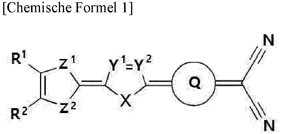 X O, S, Se, Te, SO, SO2, NRa, CRbRc oder SiRdRe ist,Y1 und Y2 unabhängig CRf oder N sind,eines von Z1 oder Z2 S ist und ein anderes von Z1 oder Z2 O, S, Se, Te oder NR9 ist,Q ein substituierter oder unsubstituierter chinoider C3- bis C30-Ring ist, wobei Q von einem 5-gliedrigen chinoiden Ring verschieden ist, der X, Y1 und Y2 beinhaltet,R1 und R2 unabhängig Wasserstoff, eine substituierte oder unsubstituierte C1- bis C30-Alkylgruppe, eine substituierte oder unsubstituierte C1- bis C30-Alkoxygruppe, eine substituierte oder unsubstituierte C1- bis C30-Alkylthiogruppe, eine substituierte oder unsubstituierte C6- bis C30-Arylgruppe, eine substituierte oder unsubstituierte heterocyclische C3- bis C30-Gruppe, eine substituierte oder unsubstituierte Silylgruppe, ein Halogen oder eine Kombination davon sind,Ra und Rg unabhängig Wasserstoff, eine substituierte oder unsubstituierte C1- bis C30-Alkylgruppe, eine substituierte oder unsubstituierte C1- bis C30-Alkoxgruppe, eine substituierte oder unsubstituierte C6- bis C30-Arylgruppe, eine substituierte oder unsubstituierte heterocyclische C3- bis C30-Gruppe, eine substituierte oder unsubstituierte Silylgruppe, ein Halogen, eine Cyanogruppe oder eine Kombination davon sind,R1 und R2 unabhängig vorhanden sind oder miteinander verbunden sind, um einen Ring zu bilden,Rb und Rc unabhängig vorhanden sind oder miteinander verbunden sind, um einen Ring zu bilden,Rd und Re unabhängig vorhanden sind oder miteinander verbunden sind, um einen Ring zu bilden,benachbarte Rf unabhängig vorhanden sind oder miteinander verbunden sind, um einen Ring zu bilden, undder Substituent des substituierten chinoiden C3- bis C30-Rings, der C1- bis C30-Alkylgruppe, der C1- bis C30-Alkoxygruppe, der C1- bis C30-Alkylthiogruppe, der C6- bis C30-Arylgruppe, der heterocyclischen C3- bis C30-Gruppe und der Silylgruppe ausgewählt ist aus:
einem Halogenatom, einer Hydroxygruppe, einer Alkoxygruppe, einer Nitrogruppe, einer Cyanogruppe, einer Aminogruppe, einer Azidogruppe, einer Amidinogruppe, einer Hydrazinogruppe, einer Hydrazonogruppe, einer Carbonylgruppe, einer Carbamylgruppe, einer Thiolgruppe, einer Estergruppe, einer Carboxylgruppe oder einem Salz davon, einer Sulfonsäuregruppe oder einem Salz davon, einer Phosphorsäuregruppe oder einem Salz davon, einer Silylgruppe, einer C1- bis C20-Alkylgruppe, einer C2- bis C20-Alkenylgruppe, einer C2- bis C20-Alkinylgruppe, einer C6- bis C30-Arylgruppe, einer C7- bis C30-Arylalkylgruppe, einer C1-bis C30-Alkoxygruppe, einer C1-bis C30-Alkylthiogruppe, einer C1- bis C20-Heteroalkylgruppe, einer C3- bis C20-Heteroarylgruppe, einer C3- bis C20-Heteroarylalkylgruppe, einer C3- bis C30-Cycloalkylgruppe, einer C3- bis C15-Cycloalkenylgruppe, einer C6- bis C15-Cycloalkinylgruppe, einer C3- bis C30-Heterocycloalkylgruppe oder einer Kombination davon. - Verbindung nach Anspruch 1, wobei Q von chemischer Formel 1 mindestens einen substituierten oder unsubstituierten 5-gliedrigen chinoiden Ring, mindestens einen substituierten oder unsubstituierten 6-gliedrigen chinoiden Ring oder einen kondensierten Ring davon beinhaltet; und/oder
wobei X, Z1 und Z2 von chemischer Formel 1 jeweils S sind. - Verbindung nach Anspruch 1 oder 2, wobei Q von chemischer Formel 1 eine der Gruppen ist, die in Gruppe 1 aufgeführt sind:

 W1 von X verschieden ist und S, Se oder Te ist,W2 bis W13 unabhängig S, Se oder Te sind,R3 und R46 unabhängig Wasserstoff, eine substituierte oder unsubstituierte C1- bis C30-Alkylgruppe, eine substituierte oder unsubstituierte C1- bis C30-Alkoxygruppe, eine substituierte oder unsubstituierte C6- bis C30-Arylgruppe, eine substituierte oder unsubstituierte heterocyclische C3- bis C30-Gruppe, eine substituierte oder unsubstituierte Silylgruppe, ein Halogen, eine Cyanogruppe oder eine Kombination davon sind,R3 bis R46 unabhängig vorhanden sind, oder zwei benachbarte R3 bis R46 miteinander verbunden sind, um einen Ring bereitzustellen, und* ein Anschlusspunkt mit chemischer Formel 1 ist.
 - Verbindung nach einem der Ansprüche 1-3, wobei die Verbindung durch eine von chemischer Formel 1A bis 11 dargestellt ist:


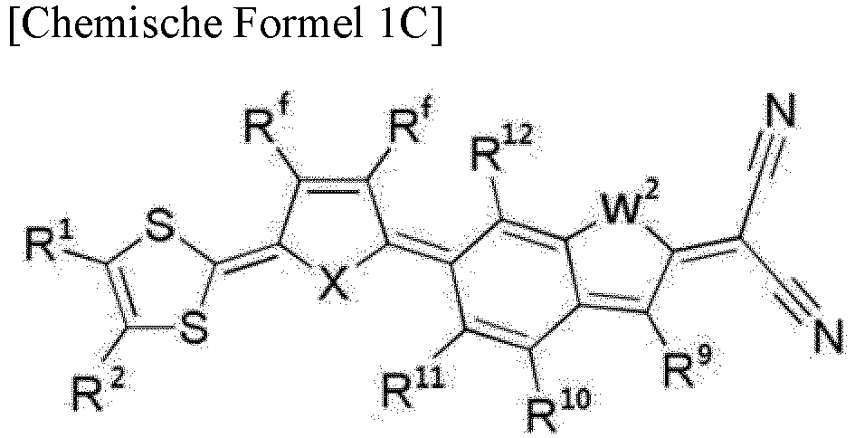

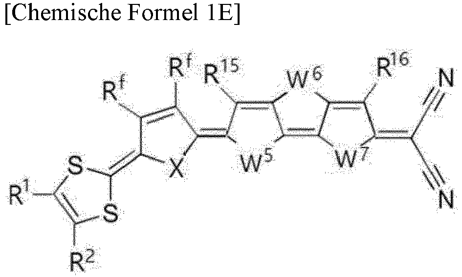


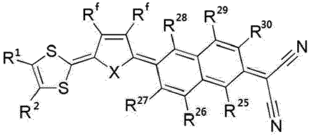

 X O, S, Se, Te, SO, SO2, NRa, CRbRc oder SiRdRe ist, wobei Ra bis Re unabhängig Wasserstoff, eine substituierte oder unsubstituierte C1- bis C30-Alkylgruppe, eine substituierte oder unsubstituierte C1- bis C30-Alkoxygruppe, eine substituierte oder unsubstituierte C6- bis C30-Arylgruppe, eine substituierte oder unsubstituierte heterocyclische C3- bis C30-Gruppe, eine substituierte oder unsubstituierte Silylgruppe, ein Halogen, eine Cyanogruppe oder eine Kombination davon sind,W2 bis W9, W12 und W13 unabhängig S, Se oder Te sind,R1 und R2 unabhängig Wasserstoff, eine substituierte oder unsubstituierte C1- bis C30-Alkylgruppe, eine substituierte oder unsubstituierte C1- bis C30-Alkoxygruppe, eine substituierte oder unsubstituierte C1- bis C30-Alkylthiogruppe, eine substituierte oder unsubstituierte C6- bis C30-Arylgruppe, eine substituierte oder unsubstituierte heterocyclische C3- bis C30-Gruppe, eine substituierte oder unsubstituierte Silylgruppe, ein Halogen oder eine Kombination davon sind, undR3 bis R6, R9 bis R20, R25 bis R30, R43 bis R46 und Rf unabhängig Wasserstoff, eine substituierte oder unsubstituierte C1- bis C30-Alkylgruppe, eine substituierte oder unsubstituierte C1- bis C30-Alkoxygruppe, eine substituierte oder unsubstituierte C6- bis C30-Arylgruppe, eine substituierte oder unsubstituierte heterocyclische C3- bis C30-Gruppe, eine substituierte oder unsubstituierte Silylgruppe, ein Halogen, eine Cyanogruppe oder eine Kombination davon sind; oderwobei die Verbindung durch eine von chemischer Formel 1A-1 bis 11-1 dargestellt ist:


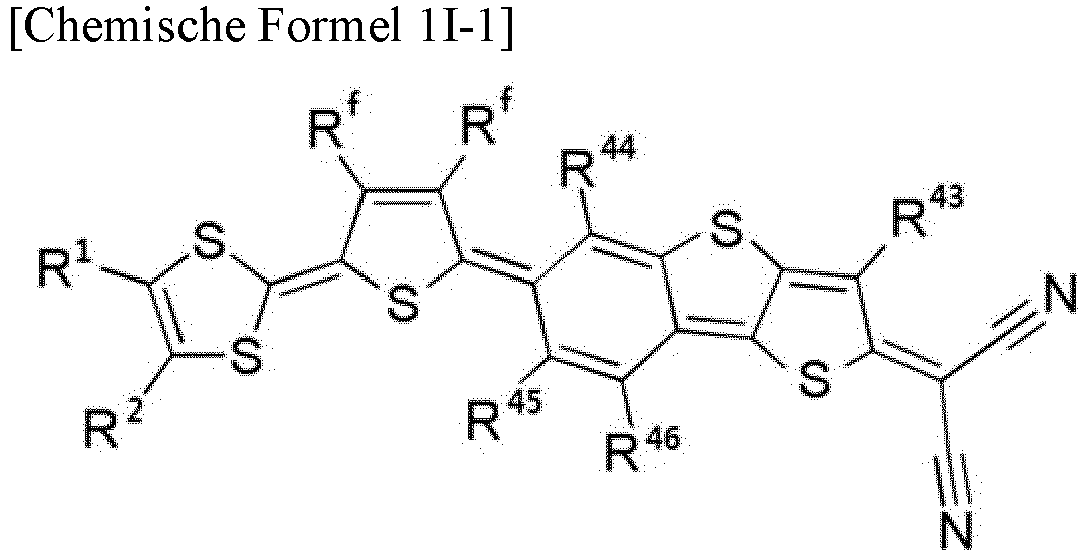 R1 und R2 unabhängig Wasserstoff, eine substituierte oder unsubstituierte C1- bis C30-Alkylgruppe, eine substituierte oder unsubstituierte C1- bis C30-Alkoxygruppe, eine substituierte oder unsubstituierte C1- bis C30-Alkylthiogruppe, eine substituierte oder unsubstituierte C6- bis C30-Arylgruppe, eine substituierte oder unsubstituierte heterocyclische C3- bis C30-Gruppe, eine substituierte oder unsubstituierte Silylgruppe, ein Halogen oder eine Kombination davon sind, undR3 bis R6, R9 bis R20, R25 bis R30, R43 bis R46 und Rf unabhängig Wasserstoff, eine substituierte oder unsubstituierte C1- bis C30-Alkylgruppe, eine substituierte oder unsubstituierte C1- bis C30-Alkoxgruppe, eine substituierte oder unsubstituierte C6- bis C30-Arylgruppe, eine substituierte oder unsubstituierte heterocyclische C3- bis C30-Gruppe, eine substituierte oder unsubstituierte Silylgruppe, ein Halogen, eine Cyanogruppe oder eine Kombination davon sind.
 - Film, umfassend die Verbindung nach einem der Ansprüche 1-4;
vorzugsweise wobei der Film eine Peak-Absorptionswellenlänge in einem Wellenlängenspektrum von 800 nm bis 3000 nm aufweist. - Infrarotsensor, umfassend:eine erste Elektrode und eine zweite Elektrode, die einander zugewandt sind, undeine organische Schicht zwischen der ersten Elektrode und der zweiten Elektrode, wobei die organische Schicht die Verbindung nach einem der Ansprüche 1-4 beinhaltet;vorzugsweise ferner umfassend ein Halbleitersubstrat.
- Infrarotsensor nach Anspruch 6, wobei der Infrarotsensor ein Peak des externen Quantenwirkungsgrads (EQE) in Bezug auf einfallendes Licht bei einer Peak-EQE-Wellenlänge aufweist, die zu einem Wellenlängenbereich von 800 nm bis 3000 nm gehört; und/oder
wobei die organische Schicht eine fotoelektrische Infrarot-Konversionsschicht umfasst, und die fotoelektrische Infrarot-Konversionsschicht die Verbindung und ein Gegenmaterial umfasst, das einen pn-Übergang mit der Verbindung bildet. - Infrarotsensor nach Anspruch 6 oder 7, wobei die organische Schicht Folgendes umfasst:eine photoelektrische Infrarot-Konversionsschicht, undeine Hilfsschicht, die mindestens eines vonzwischen der ersten Elektrode und der photoelektrischen Infrarot-Konversionsschicht, oderzwischen der zweiten Elektrode und der photoelektrischen Infrarot-Konversionsschicht ist.
- Infrarotsensor nach Anspruch 8, wobei die Hilfsschicht die Verbindung umfasst; und/oder
wobei die photoelektrische Infrarot-Konversionsschicht die Verbindung beinhaltet und die Hilfsschicht Ytterbium (Yb), Kalzium (Ca), Kalium (K), Barium (Ba), Magnesium (Mg), Lithiumfluorid (LiF) oder eine Legierung davon beinhaltet. - Kombinierter Sensor, umfassend:einen ersten Infrarotsensor, der der Infrarotsensor nach einem der Ansprüche 6-9 ist, undeinen zweiten Infrarotsensor, der konfiguriert ist, um einfallendes Licht in einem kürzeren Wellenlängenspektrum oder einem längeren Wellenlängenspektrum als der erste Infrarotsensor innerhalb eines Infrarot-Wellenlängenspektrums zu erkennen,wobei der erste Infrarotsensor und der zweite Infrarotsensor in einer Tiefenrichtung, die senkrecht zu einer Richtung in der Ebene des ersten Infrarotsensors ist, übereinander angeordnet sind.
- Kombinierter Sensor, umfassend:einen ersten Infrarotsensor, der der Infrarotsensor nach einem der Ansprüche 6-9 ist, undeinen Sensor für sichtbares Licht, der konfiguriert ist, um mindestens einen Teil des einfallenden Lichts in einem Wellenlängenspektrum des sichtbaren Lichts zu erkennen;vorzugsweise ferner umfassend:ein Halbleitersubstrat,wobei der Infrarotsensorparallel zu dem Sensor für sichtbares Licht entlang einer Richtung in der Ebene des Halbleitersubstrats angeordnet ist, odermit dem Sensor für sichtbares Licht entlang einer Tiefenrichtung des Halbleitersubstrats übereinander angeordnet ist.
- Kombinierter Sensor nach Anspruch 11, wobeider Sensor für sichtbares Licht einen blauen Sensor, der konfiguriert ist, um Licht in einem blauen Wellenlängenspektrum zu erfassen, einen grünen Sensor, der konfiguriert ist, um Licht in einem grünen Wellenlängenspektrum zu erfassen, und einen roten Sensor, der konfiguriert ist, um Licht in einem roten Wellenlängenspektrum zu erfassen, beinhaltet, undder blaue Sensor, der grüne Sensor und der rote Sensor jeweils eine in ein Halbleitersubstrat integrierte Photodiode sind.
- Kombinierter Sensor nach Anspruch 11 oder 12, wobeider Sensor für sichtbares Licht einen blauen Sensor, der konfiguriert ist, um Licht in einem blauen Wellenlängenspektrum zu erfassen, einen grünen Sensor, der konfiguriert ist, um Licht in einem grünen Wellenlängenspektrum zu erfassen, und einen roten Sensor, der konfiguriert ist, um Licht in einem roten Wellenlängenspektrum zu erfassen, beinhaltet,zwei von dem blauen Sensor, dem grünen Sensor oder dem roten Sensor Photodioden sind, die in ein Halbleitersubstrat integriert sind, undein anderer von dem blauen Sensor, dem grünen Sensor oder dem roten Sensor eine photoelektrische Konversionsvorrichtung für sichtbares Licht auf dem Halbleitersubstrat und mit dem Infrarotsensor in einer Tiefenrichtung übereinander angeordnet ist, die senkrecht zu einer Richtung in der Ebene des Infrarotsensors ist.
- Kombinierter Sensor nach einem der Ansprüche 11-13, wobeider Sensor für sichtbares Licht einen blauen Sensor, der konfiguriert ist, um Licht in einem blauen Wellenlängenspektrum zu erfassen, einen grünen Sensor, der konfiguriert ist, um Licht in einem grünen Wellenlängenspektrum zu erfassen, und einen roten Sensor, der konfiguriert ist, um Licht in einem roten Wellenlängenspektrum zu erfassen, beinhaltet,der blaue Sensor, der grüne Sensor und der rote Sensor jeweils eine photoelektrische Konversionsvorrichtung für sichtbares Licht sind, die mit dem Infrarotsensor übereinander angeordnet ist.
- Elektronische Vorrichtung, umfassend den Film nach Anspruch 5, den Infrarotsensor nach einem der Ansprüche 6-9 oder den kombinierten Sensor nach einem der Ansprüche 10-14.
Applications Claiming Priority (1)
| Application Number | Priority Date | Filing Date | Title |
|---|---|---|---|
| KR20200110629 | 2020-08-31 |
Publications (2)
| Publication Number | Publication Date |
|---|---|
| EP3960738A1 EP3960738A1 (de) | 2022-03-02 |
| EP3960738B1 true EP3960738B1 (de) | 2024-02-14 |
Family
ID=77431164
Family Applications (1)
| Application Number | Title | Priority Date | Filing Date |
|---|---|---|---|
| EP21192304.0A Active EP3960738B1 (de) | 2020-08-31 | 2021-08-20 | Verbindung, film und ir-sensor sowie kombinationssensor und elektronische vorrichtung |
Country Status (4)
| Country | Link |
|---|---|
| US (1) | US11578082B2 (de) |
| EP (1) | EP3960738B1 (de) |
| KR (1) | KR20220029429A (de) |
| CN (1) | CN114105965A (de) |
Families Citing this family (3)
| Publication number | Priority date | Publication date | Assignee | Title |
|---|---|---|---|---|
| EP3474328B1 (de) * | 2017-10-20 | 2021-09-29 | Samsung Electronics Co., Ltd. | Kombinationssensoren und elektronische vorrichtungen |
| EP3628156A1 (de) * | 2018-09-28 | 2020-04-01 | Basf Se | Verfahren zur bekämpfung von schädlingen von zuckerrohr-, zitrus-, raps- und kartoffelpflanzen |
| US20230125778A1 (en) * | 2021-10-27 | 2023-04-27 | Samsung Electronics Co., Ltd. | Compound, film, sensor, and electronic device |
Family Cites Families (4)
| Publication number | Priority date | Publication date | Assignee | Title |
|---|---|---|---|---|
| DE102010030500A1 (de) | 2010-06-24 | 2011-12-29 | Heliatek Gmbh | Verdampfbares organisch halbleitendes Material und dessen Verwendung in einem optoelektronischen Bauelement |
| DE102013101712B4 (de) | 2013-02-21 | 2020-05-28 | Heliatek Gmbh | Photoaktives organisches Material für optoelektronische Bauelemente |
| DE102015101768A1 (de) | 2015-02-06 | 2016-08-11 | Technische Universität Dresden | Lichtabsorber |
| CN112859207A (zh) | 2015-12-17 | 2021-05-28 | 富士胶片株式会社 | 近红外线吸收性组合物、膜、红外线截止滤波器、固体摄像元件、红外线吸收剂及化合物 |
-
2021
- 2021-08-20 US US17/407,646 patent/US11578082B2/en active Active
- 2021-08-20 EP EP21192304.0A patent/EP3960738B1/de active Active
- 2021-08-24 KR KR1020210111788A patent/KR20220029429A/ko active Search and Examination
- 2021-08-26 CN CN202110986771.2A patent/CN114105965A/zh active Pending
Also Published As
| Publication number | Publication date |
|---|---|
| US20220064182A1 (en) | 2022-03-03 |
| US11578082B2 (en) | 2023-02-14 |
| EP3960738A1 (de) | 2022-03-02 |
| KR20220029429A (ko) | 2022-03-08 |
| CN114105965A (zh) | 2022-03-01 |
Similar Documents
| Publication | Publication Date | Title |
|---|---|---|
| EP3960738B1 (de) | Verbindung, film und ir-sensor sowie kombinationssensor und elektronische vorrichtung | |
| EP3493262B1 (de) | Photoelektrische vorrichtungen und bildsensoren und elektronische vorrichtungen | |
| EP3798270A1 (de) | Nahinfrarotabsorber, nahinfrarotabsorbierende/-blockierende folien, photoelektrische vorrichtungen, organische sensoren und elektronische vorrichtungen | |
| KR102282495B1 (ko) | 화합물, 유기 광전자 소자 및 이미지 센서 | |
| EP4006976A1 (de) | Bildsensor | |
| US20160013426A1 (en) | Photoelectric conversion element, imaging device, optical sensor, and method of using photoelectric conversion element | |
| KR102258497B1 (ko) | 유기 광전 소자, 이미지 센서 및 전자 장치 | |
| KR102232972B1 (ko) | 광전 변환 소자, 광센서, 촬상 소자, 및 화합물 | |
| US20200136063A1 (en) | Compound and film and photoelectric diode and organic sensor and electronic device | |
| US11591347B2 (en) | Compounds and films and photoelectric diodes and organic sensors and electronic devices | |
| US11849595B2 (en) | Near-infrared absorbers, near-infrared absorbing/blocking films and photoelectric devices and organic sensors and electronic devices | |
| US11858950B2 (en) | Compound and film and photoelectric diode and organic sensor and electronic device | |
| KR20210055399A (ko) | n-형 반도체 및 이를 포함하는 유기 광전 소자, 이미지 센서 및 전자 장치 | |
| EP3993052A1 (de) | Sensor und elektronische vorrichtung | |
| EP3643712B1 (de) | Verbindung und film sowie fotoelektrische diode und organischer sensor und elektronische vorrichtung | |
| US11820859B2 (en) | Infrared absorbing polymer, infrared absorbing/blocking film, photoelectric device, organic sensor, and electronic device | |
| EP4174063A1 (de) | Verbindung, film, sensor und elektronische vorrichtung | |
| US20220059772A1 (en) | Compounds, infrared absorbers, infrared absorbing/blocking films, photoelectric devices, sensors, and electronic devices | |
| KR20200057401A (ko) | 플러렌 유도체 및 이를 포함하는 유기 광전 소자, 이미지 센서 및 전자 장치 | |
| KR20190007200A (ko) | 플러렌 유도체, 광전 소자 및 이미지 센서 |
Legal Events
| Date | Code | Title | Description |
|---|---|---|---|
| PUAI | Public reference made under article 153(3) epc to a published international application that has entered the european phase |
Free format text: ORIGINAL CODE: 0009012 |
|
| STAA | Information on the status of an ep patent application or granted ep patent |
Free format text: STATUS: THE APPLICATION HAS BEEN PUBLISHED |
|
| AK | Designated contracting states |
Kind code of ref document: A1 Designated state(s): AL AT BE BG CH CY CZ DE DK EE ES FI FR GB GR HR HU IE IS IT LI LT LU LV MC MK MT NL NO PL PT RO RS SE SI SK SM TR |
|
| STAA | Information on the status of an ep patent application or granted ep patent |
Free format text: STATUS: REQUEST FOR EXAMINATION WAS MADE |
|
| 17P | Request for examination filed |
Effective date: 20220819 |
|
| RBV | Designated contracting states (corrected) |
Designated state(s): AL AT BE BG CH CY CZ DE DK EE ES FI FR GB GR HR HU IE IS IT LI LT LU LV MC MK MT NL NO PL PT RO RS SE SI SK SM TR |
|
| P01 | Opt-out of the competence of the unified patent court (upc) registered |
Effective date: 20230519 |
|
| GRAP | Despatch of communication of intention to grant a patent |
Free format text: ORIGINAL CODE: EPIDOSNIGR1 |
|
| STAA | Information on the status of an ep patent application or granted ep patent |
Free format text: STATUS: GRANT OF PATENT IS INTENDED |
|
| INTG | Intention to grant announced |
Effective date: 20230818 |
|
| GRAS | Grant fee paid |
Free format text: ORIGINAL CODE: EPIDOSNIGR3 |
|
| GRAA | (expected) grant |
Free format text: ORIGINAL CODE: 0009210 |
|
| STAA | Information on the status of an ep patent application or granted ep patent |
Free format text: STATUS: THE PATENT HAS BEEN GRANTED |
|
| AK | Designated contracting states |
Kind code of ref document: B1 Designated state(s): AL AT BE BG CH CY CZ DE DK EE ES FI FR GB GR HR HU IE IS IT LI LT LU LV MC MK MT NL NO PL PT RO RS SE SI SK SM TR |
|
| REG | Reference to a national code |
Ref country code: GB Ref legal event code: FG4D |
|
| REG | Reference to a national code |
Ref country code: CH Ref legal event code: EP |
|
| REG | Reference to a national code |
Ref country code: DE Ref legal event code: R096 Ref document number: 602021009343 Country of ref document: DE |
|
| REG | Reference to a national code |
Ref country code: IE Ref legal event code: FG4D |
|
| REG | Reference to a national code |
Ref country code: LT Ref legal event code: MG9D |
|
| REG | Reference to a national code |
Ref country code: NL Ref legal event code: MP Effective date: 20240214 |
|
| PG25 | Lapsed in a contracting state [announced via postgrant information from national office to epo] |
Ref country code: IS Free format text: LAPSE BECAUSE OF FAILURE TO SUBMIT A TRANSLATION OF THE DESCRIPTION OR TO PAY THE FEE WITHIN THE PRESCRIBED TIME-LIMIT Effective date: 20240614 |
|
| PG25 | Lapsed in a contracting state [announced via postgrant information from national office to epo] |
Ref country code: LT Free format text: LAPSE BECAUSE OF FAILURE TO SUBMIT A TRANSLATION OF THE DESCRIPTION OR TO PAY THE FEE WITHIN THE PRESCRIBED TIME-LIMIT Effective date: 20240214 |
|
| PG25 | Lapsed in a contracting state [announced via postgrant information from national office to epo] |
Ref country code: GR Free format text: LAPSE BECAUSE OF FAILURE TO SUBMIT A TRANSLATION OF THE DESCRIPTION OR TO PAY THE FEE WITHIN THE PRESCRIBED TIME-LIMIT Effective date: 20240515 |
|
| REG | Reference to a national code |
Ref country code: AT Ref legal event code: MK05 Ref document number: 1656962 Country of ref document: AT Kind code of ref document: T Effective date: 20240214 |
|
| PG25 | Lapsed in a contracting state [announced via postgrant information from national office to epo] |
Ref country code: RS Free format text: LAPSE BECAUSE OF FAILURE TO SUBMIT A TRANSLATION OF THE DESCRIPTION OR TO PAY THE FEE WITHIN THE PRESCRIBED TIME-LIMIT Effective date: 20240514 Ref country code: NL Free format text: LAPSE BECAUSE OF FAILURE TO SUBMIT A TRANSLATION OF THE DESCRIPTION OR TO PAY THE FEE WITHIN THE PRESCRIBED TIME-LIMIT Effective date: 20240214 Ref country code: HR Free format text: LAPSE BECAUSE OF FAILURE TO SUBMIT A TRANSLATION OF THE DESCRIPTION OR TO PAY THE FEE WITHIN THE PRESCRIBED TIME-LIMIT Effective date: 20240214 |
|
| PG25 | Lapsed in a contracting state [announced via postgrant information from national office to epo] |
Ref country code: ES Free format text: LAPSE BECAUSE OF FAILURE TO SUBMIT A TRANSLATION OF THE DESCRIPTION OR TO PAY THE FEE WITHIN THE PRESCRIBED TIME-LIMIT Effective date: 20240214 |
|
| PG25 | Lapsed in a contracting state [announced via postgrant information from national office to epo] |
Ref country code: AT Free format text: LAPSE BECAUSE OF FAILURE TO SUBMIT A TRANSLATION OF THE DESCRIPTION OR TO PAY THE FEE WITHIN THE PRESCRIBED TIME-LIMIT Effective date: 20240214 |
|
| PG25 | Lapsed in a contracting state [announced via postgrant information from national office to epo] |
Ref country code: RS Free format text: LAPSE BECAUSE OF FAILURE TO SUBMIT A TRANSLATION OF THE DESCRIPTION OR TO PAY THE FEE WITHIN THE PRESCRIBED TIME-LIMIT Effective date: 20240514 Ref country code: NO Free format text: LAPSE BECAUSE OF FAILURE TO SUBMIT A TRANSLATION OF THE DESCRIPTION OR TO PAY THE FEE WITHIN THE PRESCRIBED TIME-LIMIT Effective date: 20240514 Ref country code: NL Free format text: LAPSE BECAUSE OF FAILURE TO SUBMIT A TRANSLATION OF THE DESCRIPTION OR TO PAY THE FEE WITHIN THE PRESCRIBED TIME-LIMIT Effective date: 20240214 Ref country code: LT Free format text: LAPSE BECAUSE OF FAILURE TO SUBMIT A TRANSLATION OF THE DESCRIPTION OR TO PAY THE FEE WITHIN THE PRESCRIBED TIME-LIMIT Effective date: 20240214 Ref country code: IS Free format text: LAPSE BECAUSE OF FAILURE TO SUBMIT A TRANSLATION OF THE DESCRIPTION OR TO PAY THE FEE WITHIN THE PRESCRIBED TIME-LIMIT Effective date: 20240614 Ref country code: HR Free format text: LAPSE BECAUSE OF FAILURE TO SUBMIT A TRANSLATION OF THE DESCRIPTION OR TO PAY THE FEE WITHIN THE PRESCRIBED TIME-LIMIT Effective date: 20240214 Ref country code: GR Free format text: LAPSE BECAUSE OF FAILURE TO SUBMIT A TRANSLATION OF THE DESCRIPTION OR TO PAY THE FEE WITHIN THE PRESCRIBED TIME-LIMIT Effective date: 20240515 Ref country code: FI Free format text: LAPSE BECAUSE OF FAILURE TO SUBMIT A TRANSLATION OF THE DESCRIPTION OR TO PAY THE FEE WITHIN THE PRESCRIBED TIME-LIMIT Effective date: 20240214 Ref country code: ES Free format text: LAPSE BECAUSE OF FAILURE TO SUBMIT A TRANSLATION OF THE DESCRIPTION OR TO PAY THE FEE WITHIN THE PRESCRIBED TIME-LIMIT Effective date: 20240214 Ref country code: BG Free format text: LAPSE BECAUSE OF FAILURE TO SUBMIT A TRANSLATION OF THE DESCRIPTION OR TO PAY THE FEE WITHIN THE PRESCRIBED TIME-LIMIT Effective date: 20240214 Ref country code: AT Free format text: LAPSE BECAUSE OF FAILURE TO SUBMIT A TRANSLATION OF THE DESCRIPTION OR TO PAY THE FEE WITHIN THE PRESCRIBED TIME-LIMIT Effective date: 20240214 |
|
| PGFP | Annual fee paid to national office [announced via postgrant information from national office to epo] |
Ref country code: FR Payment date: 20240611 Year of fee payment: 4 |
|
| PG25 | Lapsed in a contracting state [announced via postgrant information from national office to epo] |
Ref country code: PL Free format text: LAPSE BECAUSE OF FAILURE TO SUBMIT A TRANSLATION OF THE DESCRIPTION OR TO PAY THE FEE WITHIN THE PRESCRIBED TIME-LIMIT Effective date: 20240214 Ref country code: PT Free format text: LAPSE BECAUSE OF FAILURE TO SUBMIT A TRANSLATION OF THE DESCRIPTION OR TO PAY THE FEE WITHIN THE PRESCRIBED TIME-LIMIT Effective date: 20240614 |
|
| PG25 | Lapsed in a contracting state [announced via postgrant information from national office to epo] |
Ref country code: SE Free format text: LAPSE BECAUSE OF FAILURE TO SUBMIT A TRANSLATION OF THE DESCRIPTION OR TO PAY THE FEE WITHIN THE PRESCRIBED TIME-LIMIT Effective date: 20240214 Ref country code: PT Free format text: LAPSE BECAUSE OF FAILURE TO SUBMIT A TRANSLATION OF THE DESCRIPTION OR TO PAY THE FEE WITHIN THE PRESCRIBED TIME-LIMIT Effective date: 20240614 Ref country code: PL Free format text: LAPSE BECAUSE OF FAILURE TO SUBMIT A TRANSLATION OF THE DESCRIPTION OR TO PAY THE FEE WITHIN THE PRESCRIBED TIME-LIMIT Effective date: 20240214 Ref country code: LV Free format text: LAPSE BECAUSE OF FAILURE TO SUBMIT A TRANSLATION OF THE DESCRIPTION OR TO PAY THE FEE WITHIN THE PRESCRIBED TIME-LIMIT Effective date: 20240214 |