EP3958464A2 - Phase synchronized lo generation - Google Patents
Phase synchronized lo generation Download PDFInfo
- Publication number
- EP3958464A2 EP3958464A2 EP20188261.0A EP20188261A EP3958464A2 EP 3958464 A2 EP3958464 A2 EP 3958464A2 EP 20188261 A EP20188261 A EP 20188261A EP 3958464 A2 EP3958464 A2 EP 3958464A2
- Authority
- EP
- European Patent Office
- Prior art keywords
- reset signal
- clock
- dffs
- clock signal
- coupled
- Prior art date
- Legal status (The legal status is an assumption and is not a legal conclusion. Google has not performed a legal analysis and makes no representation as to the accuracy of the status listed.)
- Pending
Links
Images





Classifications
-
- H—ELECTRICITY
- H03—ELECTRONIC CIRCUITRY
- H03L—AUTOMATIC CONTROL, STARTING, SYNCHRONISATION OR STABILISATION OF GENERATORS OF ELECTRONIC OSCILLATIONS OR PULSES
- H03L7/00—Automatic control of frequency or phase; Synchronisation
- H03L7/06—Automatic control of frequency or phase; Synchronisation using a reference signal applied to a frequency- or phase-locked loop
- H03L7/16—Indirect frequency synthesis, i.e. generating a desired one of a number of predetermined frequencies using a frequency- or phase-locked loop
- H03L7/18—Indirect frequency synthesis, i.e. generating a desired one of a number of predetermined frequencies using a frequency- or phase-locked loop using a frequency divider or counter in the loop
-
- G—PHYSICS
- G06—COMPUTING OR CALCULATING; COUNTING
- G06F—ELECTRIC DIGITAL DATA PROCESSING
- G06F1/00—Details not covered by groups G06F3/00 - G06F13/00 and G06F21/00
- G06F1/04—Generating or distributing clock signals or signals derived directly therefrom
- G06F1/06—Clock generators producing several clock signals
-
- G—PHYSICS
- G06—COMPUTING OR CALCULATING; COUNTING
- G06F—ELECTRIC DIGITAL DATA PROCESSING
- G06F1/00—Details not covered by groups G06F3/00 - G06F13/00 and G06F21/00
- G06F1/04—Generating or distributing clock signals or signals derived directly therefrom
- G06F1/10—Distribution of clock signals, e.g. skew
-
- G—PHYSICS
- G06—COMPUTING OR CALCULATING; COUNTING
- G06F—ELECTRIC DIGITAL DATA PROCESSING
- G06F1/00—Details not covered by groups G06F3/00 - G06F13/00 and G06F21/00
- G06F1/04—Generating or distributing clock signals or signals derived directly therefrom
- G06F1/12—Synchronisation of different clock signals provided by a plurality of clock generators
-
- H—ELECTRICITY
- H03—ELECTRONIC CIRCUITRY
- H03K—PULSE TECHNIQUE
- H03K21/00—Details of pulse counters or frequency dividers
- H03K21/08—Output circuits
- H03K21/10—Output circuits comprising logic circuits
-
- H—ELECTRICITY
- H03—ELECTRONIC CIRCUITRY
- H03K—PULSE TECHNIQUE
- H03K23/00—Pulse counters comprising counting chains; Frequency dividers comprising counting chains
- H03K23/40—Gating or clocking signals applied to all stages, i.e. synchronous counters
- H03K23/42—Out-of-phase gating or clocking signals applied to counter stages
- H03K23/44—Out-of-phase gating or clocking signals applied to counter stages using field-effect transistors
-
- H—ELECTRICITY
- H03—ELECTRONIC CIRCUITRY
- H03K—PULSE TECHNIQUE
- H03K23/00—Pulse counters comprising counting chains; Frequency dividers comprising counting chains
- H03K23/40—Gating or clocking signals applied to all stages, i.e. synchronous counters
- H03K23/50—Gating or clocking signals applied to all stages, i.e. synchronous counters using bi-stable regenerative trigger circuits
- H03K23/54—Ring counters, i.e. feedback shift register counters
-
- H—ELECTRICITY
- H03—ELECTRONIC CIRCUITRY
- H03K—PULSE TECHNIQUE
- H03K3/00—Circuits for generating electric pulses; Monostable, bistable or multistable circuits
- H03K3/02—Generators characterised by the type of circuit or by the means used for producing pulses
- H03K3/027—Generators characterised by the type of circuit or by the means used for producing pulses by the use of logic circuits, with internal or external positive feedback
- H03K3/037—Bistable circuits
-
- H—ELECTRICITY
- H03—ELECTRONIC CIRCUITRY
- H03K—PULSE TECHNIQUE
- H03K5/00—Manipulating of pulses not covered by one of the other main groups of this subclass
- H03K5/13—Arrangements having a single output and transforming input signals into pulses delivered at desired time intervals
- H03K5/133—Arrangements having a single output and transforming input signals into pulses delivered at desired time intervals using a chain of active delay devices
-
- H—ELECTRICITY
- H03—ELECTRONIC CIRCUITRY
- H03K—PULSE TECHNIQUE
- H03K5/00—Manipulating of pulses not covered by one of the other main groups of this subclass
- H03K5/13—Arrangements having a single output and transforming input signals into pulses delivered at desired time intervals
- H03K5/135—Arrangements having a single output and transforming input signals into pulses delivered at desired time intervals by the use of time reference signals, e.g. clock signals
-
- H—ELECTRICITY
- H03—ELECTRONIC CIRCUITRY
- H03K—PULSE TECHNIQUE
- H03K5/00—Manipulating of pulses not covered by one of the other main groups of this subclass
- H03K5/13—Arrangements having a single output and transforming input signals into pulses delivered at desired time intervals
- H03K5/14—Arrangements having a single output and transforming input signals into pulses delivered at desired time intervals by the use of delay lines
-
- H—ELECTRICITY
- H03—ELECTRONIC CIRCUITRY
- H03L—AUTOMATIC CONTROL, STARTING, SYNCHRONISATION OR STABILISATION OF GENERATORS OF ELECTRONIC OSCILLATIONS OR PULSES
- H03L7/00—Automatic control of frequency or phase; Synchronisation
- H03L7/06—Automatic control of frequency or phase; Synchronisation using a reference signal applied to a frequency- or phase-locked loop
- H03L7/08—Details of the phase-locked loop
- H03L7/0805—Details of the phase-locked loop the loop being adapted to provide an additional control signal for use outside the loop
-
- H—ELECTRICITY
- H03—ELECTRONIC CIRCUITRY
- H03L—AUTOMATIC CONTROL, STARTING, SYNCHRONISATION OR STABILISATION OF GENERATORS OF ELECTRONIC OSCILLATIONS OR PULSES
- H03L7/00—Automatic control of frequency or phase; Synchronisation
- H03L7/06—Automatic control of frequency or phase; Synchronisation using a reference signal applied to a frequency- or phase-locked loop
- H03L7/08—Details of the phase-locked loop
- H03L7/0807—Details of the phase-locked loop concerning mainly a recovery circuit for the reference signal
-
- H—ELECTRICITY
- H03—ELECTRONIC CIRCUITRY
- H03L—AUTOMATIC CONTROL, STARTING, SYNCHRONISATION OR STABILISATION OF GENERATORS OF ELECTRONIC OSCILLATIONS OR PULSES
- H03L7/00—Automatic control of frequency or phase; Synchronisation
- H03L7/06—Automatic control of frequency or phase; Synchronisation using a reference signal applied to a frequency- or phase-locked loop
- H03L7/08—Details of the phase-locked loop
- H03L7/099—Details of the phase-locked loop concerning mainly the controlled oscillator of the loop
- H03L7/0991—Details of the phase-locked loop concerning mainly the controlled oscillator of the loop the oscillator being a digital oscillator, e.g. composed of a fixed oscillator followed by a variable frequency divider
- H03L7/0992—Details of the phase-locked loop concerning mainly the controlled oscillator of the loop the oscillator being a digital oscillator, e.g. composed of a fixed oscillator followed by a variable frequency divider comprising a counter or a frequency divider
Definitions
- the external reset signal RST is enabled at logic 1 and the inverter 103 outputs logic 0, so that the switch 102 is turned off and the external clock signal CLK is blocked by the switch 102.
- the internal clock signal CLK_INT is set as logic 0 and each DFF is set in the reset mode and outputs logic 0. Accordingly, the internal reset signal RST_INT is enabled and set as logic 1 through the inverse output terminal QB of the last DFF 107.
- the reset terminals of the first DIV2 block 610 and the second DIV2 block 620 are coupled to an internal reset signal RST_INT 603 that is synchronous to the first clock signal CLK 601.
- RST_INT 603 When the internal reset signal RST_INT 603 is enabled at logic 1, both the first DIV2 block 610 and the second DIV2 block 620 are set in the reset mode, in which all internal nodes of the first DIV2 block 610 and the second DIV2 block 620 are set with predefined voltages.
Landscapes
- Engineering & Computer Science (AREA)
- Theoretical Computer Science (AREA)
- Physics & Mathematics (AREA)
- General Engineering & Computer Science (AREA)
- General Physics & Mathematics (AREA)
- Nonlinear Science (AREA)
- Electronic Switches (AREA)
- Stabilization Of Oscillater, Synchronisation, Frequency Synthesizers (AREA)
Abstract
Description
- This present disclosure claims the benefit of
U.S. Provisional Application No. 62/869,149, "PHASE SYNCHRONIZED LO GENERATION" filed on July 1, 2019 U.S. Patent Application No. 16/918,601, "PHASE SYNCHRONIZED LO GENERATION" filed on July 1, 2020 - The background description provided herein is for the purpose of generally presenting the context of the disclosure. Work of the presently named inventors, to the extent the work is described in this background section, as well as aspects of the description that may not otherwise qualify as prior art at the time of filing, are neither expressly nor impliedly admitted as prior art against the present disclosure.
- A transceiver may have multiple transmitter (TX) paths. Each path may have its own local oscillator (LO), which may be generated from a divide-by-2 (Div2) frequency divider associated with the path. Although these frequency dividers can output the same frequency LO, the phases of these LO may be different and varied, which may cause a meta-stability issue. In order to avoid the meta-stability issue, it may be desirable to synchronize different dividers so that their phase difference can be kept constant.
- Aspects of the disclosure provide an apparatus for controlling an internal reset signal that is synchronous to a clock signal. The apparatus includes a clock switch circuit and a plurality of serially coupled D flip-flops (DFFs). The clock switch circuit receiving the clock signal can output the clock signal in an on state and block the clock signal in an off state. The plurality of serially coupled DFFs are coupled to the clock switch circuit and driven by the clock signal. In response to an external reset signal being enabled, the plurality of serially coupled DFFs can enable the internal reset signal. After a predefined number of clock signal cycles after the external reset signal is disabled, the plurality of serially coupled DFFs can disable the internal reset signal.
- In an embodiment, a data terminal of a first DFF in the plurality of DFFs is coupled to a logic voltage at which the internal reset signal is enabled, and an inverse output terminal of a last DFF in the plurality of DFFs is coupled to the internal reset signal.
- In an embodiment, an input terminal of the clock switch circuit is coupled to the clock signal, an output terminal of the clock switch circuit is coupled to a clock terminal of each DFF in the plurality of DFFs, and a control terminal of the clock switch is coupled to the external reset signal.
- In an embodiment, the clock switch circuit is in the off state so that the clock signal is not output to the plurality of DFFs in response to the external reset signal being enabled, and in the on state so that the clock signal is output to the plurality of DFFs in response to the external reset signal being disabled.
- In an embodiment, the external reset signal is coupled to a reset terminal of each DFF in the plurality of DFFs.
- In an embodiment, each DFF is set in a reset mode and in a standby mode in response to the external reset signal being enabled and disabled, respectively.
- In an embodiment, the predefined number of clock signal cycles is dependent on a total number of DFFs.
- Aspects of the disclosure also provide a method for controlling an internal reset signal that is synchronous to a clock signal. In the method, the clock signal is received through a clock switch circuit that is configured to output the clock signal in an on state and block the clock signal in an off state. The internal reset signal is enabled through a plurality of serially coupled D flip-flops (DFFs) in response to an external reset signal being enabled, and disabled through the plurality of serially coupled DFFs after a predefined number of clock signal cycles after the external reset signal is disabled. The plurality of serially coupled DFFs are coupled to the clock switch circuit and driven by the clock signal.
- Aspects of the disclosure also provide an electronic system including a local divider reset (LORST) circuity. The LORST circuitry receives a clock signal through a clock switch circuit that is configured to output the clock signal in an on state and block the clock signal in an off state. The LORST circuitry enables an internal reset signal through a plurality of serially coupled D flip-flops (DFFs) in response to an external reset signal being enabled, and disables the internal reset signal through the plurality of serially coupled DFFs after a predefined number of clock signal cycles after the external reset signal is disabled. The plurality of serially coupled DFFs are coupled to the clock switch circuit and driven by the clock signal.
- Various embodiments of this disclosure that are proposed as examples will be described in detail with reference to the following figures, wherein like numerals reference like elements, and wherein:
-
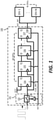
FIG. 1 shows an exemplary local divider reset (LORST) circuitry according to an embodiment of the disclosure; -
FIGs. 2A-2D show detailed operations of the LORST circuitry according to an embodiment of the disclosure; -
FIG. 3 shows an exemplary timing diagram of controlling an internal reset signal RST_INT according to an embodiment of the disclosure; -
FIG. 4 shows an exemplary timing diagram according to an embodiment of the disclosure; -
FIG. 5 shows an exemplary divider circuit block and the corresponding detailed circuitry according to an embodiment of the disclosure; -
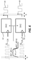
FIG. 6 shows an example of controlling two divider circuit blocks according to an embodiment of the disclosure; -
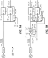
FIG. 7A shows an exemplary local LORST configuration according to an embodiment of the disclosure; -
FIG. 7B shows an exemplary cascade LORST configuration according to an embodiment of the disclosure; -
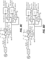
FIGs. 8A-8D show detailed operations of the cascade LORST configuration according to an embodiment of the disclosure; -
FIG. 8E show an alternative of the cascade LORST configuration according to an embodiment of the disclosure; -
FIG. 9 shows a flowchart of an exemplary process according to an embodiment of the disclosure; and -
FIGs. 10A-10C show some exemplary transceivers according to embodiments of the disclosure. -
FIG. 1 shows an exemplary local divider reset (LORST)circuitry 100 according to an embodiment of the disclosure. TheLORST circuitry 100 includes aclock switch circuit 101 and a plurality of (e.g., M) serially coupled D flip-flops (DFFs). - The
clock switch circuit 101 receives a clock signal CLK and is controlled by a reset signal RST. The clock signal CLK can be either a global clock signal or a local clock signal. The reset signal RST can be either a global reset signal or a local reset signal. In the disclosure, the clock signal CLK and the reset signal RST can be also referred to as external clock signal and external reset signal, respectively. It is noted that the external reset signal RST does not have timing information of the external clock signal CLK. That is, the external reset signal RST may not be synchronous to the external clock signal CLK. - The
clock switch circuit 101 includes aswitch 102 and an inverter 103. An input terminal of theswitch 102 is coupled to the external clock signal CLK and an output terminal of theswitch 102 is coupled to a clock terminal of each DFF in the plurality of DFFs of theLORST circuitry 100. In addition, a control terminal of theswitch 102 is coupled to an output terminal of the inverter 103. An input terminal of the inverter 103 is coupled to the external reset signal RST. - The operation of the
clock switch circuit 101 is controlled by the external reset signal RST. When the external reset signal RST is enabled, theclock switch circuit 101 can block the external clock signal CLK so that no clock signal triggers the plurality of DFFs. When the external reset signal RST is disabled, theclock switch circuit 101 can pass the external clock signal CLK to be an internal clock signal CLK_INT that triggers the plurality of DFFs. - In
FIG. 1 , it is assumed that the external reset signal RST is enabled at logic 1 (e.g., a supply voltage VCC) and disabled at logic 0 (e.g., a ground voltage GND), and theswitch 102 is turned on and off when the control terminal of theswitch 102 is set aslogic 1 andlogic 0, respectively. Accordingly, when the external reset signal RST is enabled, the inverter 103 receiveslogic 1 andoutputs logic 0, setting the control terminal of theswitch 102 aslogic 0. Therefore, theswitch 102 is turned off, and then the external clock signal CLK is blocked by theswitch 102. When the external reset signal RST is disabled, the inverter 103 receiveslogic 0 andoutputs logic 1, setting the control terminal of theswitch 102 aslogic 1. Therefore, theswitch 102 is turned on, and then the external clock signal CLK can be passed through theswitch 102 to be the internal clock signal CLK_INT that is coupled to the clock terminal of each DFF. - It is noted, in other embodiments, the external reset signal RST can be enabled at
logic 0 and disabled atlogic 1. Accordingly, theswitch 102 is turned on and off when the control terminal of theswitch 102 is set as atlogic 0 and atlogic 1, respectively. - Referring back to
FIG. 1 , each DFF in theLORST circuitry 100 includes a data terminal D, an output terminal Q (and/or an inverse output terminal QB), a reset terminal R, and a clock terminal. The plurality of DFFs is serially coupled from afirst DFF 104 to alast DFF 107. That is, a data terminal D of a current DFF (e.g. DFF 105) is coupled to an output terminal Q of a previous DFF (e.g., DFF 104), and an output terminal Q of the current DFF is coupled to a data terminal D of a next DFF (e.g., DFF106). - According to aspects of the disclosure, the
LORST circuitry 100 can output an internal reset signal RST_INT through the inverse output terminal QB of thelast DFF 107. - In the
FIG. 1 example, it is assumed that the internal reset signal RST_INT is enabled atlogic 1 and disabled atlogic 0, thus a data terminal D of thefirst DFF 104 is coupled tologic 1. However, it is noted that if the internal reset signal RST_INT is enabled atlogic 0 and disabled atlogic 1, the data terminal D of thefirst DFF 104 can be coupled to logic 0 (e.g., GND) in another example. In such an example, when the external reset signal RST is enabled, each DFF outputslogic 1 so that the internal reset signal RST_INT is set aslogic 0 through the inverse output terminal QB of thelast DFF 107. When the external reset signal RST is disabled, after M clock signal cycles, the internal reset signal RST_INT is disabled atlogic 1 due to the data terminal D of thefirst DFF 104 being coupled tologic 0. Therefore, the data terminal D of the first DFF is coupled to a logic voltage at which the internal reset signal RST_INT is enabled. - In addition, in the
LORST circuitry 100, a clock terminal and a reset terminal of each DFF are coupled to the output terminal of theswitch 102 and the external reset signal RST, respectively. The inverse output terminal QB of thelast DFF 107 is coupled to a plurality of (e.g., N) divider blocks DIV-1 ~ DIV-N in theFIG. 1 example. However, in another example, the inverse output terminal QB of thelast DFF 107 can be coupled to various circuit blocks with a reset function. - According to aspects of the disclosure, the internal reset signal RST_INT can be synchronous to the external clock signal CLK in order to reset the divider blocks DIV-1 ~ DIV-N in the
FIG. 1 example or various circuit blocks in other examples. An operation of resetting the divider blocks DIV-1 ~ DIV-N (or various circuit blocks in other examples) includes: (1) resetting all internal nodes of the divider blocks with predefined voltages; (2) using the LORST circuity to generate internal reset signal RST_INT that is synchronous to the external clock signal CLK; and (3) unlocking the divider blocks, so that the divider blocks can be free running. - Specifically, when the external reset signal RST is enabled, the external clock signal CLK is blocked, and each DFF is set in a reset mode and thus outputs
logic 0, so that the internal reset signal RST_INT is set aslogic 1 through the inverse output terminal QB of thelast DFF 107. When the external reset signal RST is disabled, each DFF is set in a standby mode and the external clock signal CLK is passed through theswitch 102 to each DFF. After a number of clock signal cycles, the internal reset signal RST_INT is flipped fromlogic 1 tologic 0. Accordingly, the internal reset signal RST_INT can be synchronous to the external clock signal CLK. The number of clock signal cycles is dependent on a total number of the DFFs. InFIG. 1 , the total number of the DFFs is M. -
FIGs. 2A-2D show detailed operations of theLORST circuitry 100 according to an embodiment of the disclosure. It is assumed that all DIV-1 ~ DIV-N blocks are set in the reset mode and in the standby mode when the internal reset signal is enabled atlogic 1 and disabled atlogic 0, respectively. - In a first step, as shown in
FIG. 2A , the external reset signal RST is enabled atlogic 1 and the inverter 103outputs logic 0, so that theswitch 102 is turned off and the external clock signal CLK is blocked by theswitch 102. The internal clock signal CLK_INT is set aslogic 0 and each DFF is set in the reset mode andoutputs logic 0. Accordingly, the internal reset signal RST_INT is enabled and set aslogic 1 through the inverse output terminal QB of thelast DFF 107. - In a second step, as shown in
FIG. 2B , the external reset signal RST transits fromlogic 1 tologic 0 after a certain number of clock signal cycles after the first step. That is, the external reset signal RST transits from the enable status to the disable status, and thus each DFF transits from the reset mode to the standby mode. However, due to the propagation delay, the inverter 103 still outputslogic 0 and thus the external clock signal CLK is still blocked by theswitch 102 so that the internal clock signal CLK_INT is still set aslogic 0. - In a third step, as shown in
FIG. 2C , theLORST circuitry 100 has completed the transition from the reset mode to the standby mode. Accordingly, the external reset signal RST is disabled atlogic 0 and the inverter 103outputs logic 1, so that theswitch 102 is turned on and the clock signal CLK is passed through theswitch 102 to initiate the internal clock signal CLK_INT. After a first clock signal cycle of the internal clock signal CLK_INT, thefirst DFF 104 is flipped fromlogic 0 tologic 1 since the data terminal D of thefirst DFF 104 is coupled to logic 1 (e.g., VCC). However, the outputs of other DFFs including thelast DFF 107 are not flipped and still set aslogic 0. Accordingly, the internal reset signal RST_INT is still enabled and set aslogic 1 through the inverse output terminal QB of thelast DFF 107. - In a fourth step, as shown in
FIG. 2D , theLORST circuitry 100 has completed M clock signal cycles after the transition from the reset mode to the standby mode. That is, the LORST circuit completes first M clock signal cycles of the internal clock signal CLK_INT. Accordingly, all outputs of the plurality of DFFs including thelast DFF 107 are flipped and set aslogic 1, the internal reset signal RST_INT is disabled and flipped fromlogic 1 tologic 0 through the inverse output terminal QB of thelast DFF 107. - Through this operation, the internal reset signal RST_INT can be synchronous to the external clock signal CLK to reset the divider blocks (or various circuit blocks in other examples) that are coupled to the internal reset signal RST_INT.
-
FIG. 3 shows an exemplary timing diagram 300 of controlling the internal reset signal RST_INT according to an embodiment of the disclosure. For simplicity, the external reset signal RST is set to be synchronous to the clock signal CLK. However, it is noted that the external reset signal RST may not be synchronous to the clock signal CLK and can be randomly enabled and disabled. - In the timing diagram 300, a waveform 301 depicts the external reset signal RST, a waveform 302 depicts the external clock signal CLK, and a
waveform 303 depicts the internal reset signal RST_INT. At T1, the external reset signal RST is enabled atlogic 1, and thus theLORST circuitry 100 is set in the reset mode, enabling the internal reset signal RST_INT. At T2, the external reset signal RST is disabled atlogic 0 and thus theLORST circuitry 100 is set in the standby mode, but the internal reset signal RST_INT is still enabled atlogic 1 since the inverse output terminal QB of thelast DFF 107 is not flipped. At T3, the internal reset signal RST_INT is disabled atlogic 0 since the inverse output terminal QB of thelast DFF 107 is flipped after a number of clock signal cycles. The number of clock signal cycles between T2 and T3 is dependent on a total number of the plurality of DFFs. -
FIG. 4 shows an exemplary timing diagram 400 according to an embodiment of the disclosure. In the timing diagram 400, a waveform 410 depicts a clock signal CLK_IN with a frequency of freq input to a divide-by-2 (DIV2) divider circuitry, which can output a divided clock signal with a frequency of freq/2. The DIV2 divider is a rising edge triggered circuitry. - It is noted that the DIV2 divider is used in the
FIG. 4 example just for simplicity, in another example, other types of divider, such as divide-by-3 (DIV3) or divide-by-4 (DIV4), can be used. - In the timing diagram 400, a
waveform 420 depicts a reset signal RST1 for resetting the DIV2 circuit block. When the reset signal RST1 is enabled atlogic 1, the DIV2 circuit block is set in the reset mode and suspends the output of the divided clock signal. When the reset signal RST1 is disabled atlogic 0, the DIV2 circuit block is set in the standby mode and resumes the output of the divided clock signal. The dived clock signal is referred to as CLK_OUT1 and depicted in awaveform 430. It is noted that the reset signal RST1 is synchronous to the input clock signal CLK_IN, and thus a fallingedge 421 at which the reset signal RST1 is disabled is synchronous to a fallingedge 411 of the input clock signal CLK_IN. After the reset signal RST1 is disabled at the fallingedge 421, the divided clock signal CLK_OUT1 starts free running at a next rising edge, i.e., risingedge 412, of the input clock signal CLK_IN. Accordingly, a risingedge 431 of a first clock of the divided clock signal CLK_OUT1 is synchronous to the risingedge 412 of the input clock signal CLK_IN. - Still referencing to the timing diagram 400, a
waveform 440 depicts a reset signal RST2 for resetting the same DIV2 circuit block. When the reset signal RST2 is enabled atlogic 1, the DIV2 circuit block is set in the reset mode and suspends the output of the divided clock signal; when the reset signal RST2 is disabled atlogic 0, the DIV2 circuit block is set in the standby mode and resumes the output of the divided clock signal. The divided clock signal is referred to as CLK_OUT2 and depicted in awaveform 450. It is noted that the reset signal RST2 is not synchronous to the input clock signal CLK_IN, and thus a fallingedge 441 at which the reset signal RST2 is disabled is not synchronous to any rising or falling edge of the input clock signal CLK_IN. After the reset signal RST2 is disabled at the fallingedge 441, the divided clock signal CLK_OUT2 starts free running at a next rising edge, i.e., risingedge 413, of the input clock signal CLK_IN. Accordingly, a risingedge 451 of a first clock of the divided clock signal CLK_OUT2 is synchronous to the risingedge 413 of the clock signal CLK_IN. - It is noted that, in the timing diagram 400, the divided clock signals CLK_OUT1 and CLK_OUT2 have complementary phases. It indicates that, a phase of a divided clock signal (e.g., CLK_OUT2) that is controlled by a randomly reset signal (e.g., RST2) can be different from or even complementary to a phase of a divided clock signal (e.g., CLK_OUT1) that is controlled by a synchronously reset signal (e.g., RST1). Therefore, for multiple divided clock signals, it is desirable to use synchronously reset signal, so that each divided clock signal can have a pre-determined phase.
-
FIG. 5 shows an exemplarydivider circuit block 500 and the corresponding detailed circuitry according to an embodiment of the disclosure. Thedivider circuit block 500 is a DIV2 block that receives through an input terminal CLK_IN an input clock signal with a frequency of freq (e.g., the input clock signal CLK_IN 410 in theFIG. 4 example) and outputs through an output terminal CLK_OUT a divided clock signal with a frequency of freq/2 (e.g., the dividedclock signal CLK_OUT1 430 in theFIG. 4 example). A reset terminal RST is used for receiving a reset signal (e.g., the reset signalRST1 420 in theFIG. 4 example) that is enabled and disabled to set thedivider circuit block 500 in the reset mode and in the standby mode, respectively. That is, when the reset signal (e.g., RST1 420) is enabled (e.g., at logic 1), the divided clock signal (e.g., CLK_OUT1 430) is turned off and each internal nodes of thedivider circuit block 500 is set with a respective predefined charge. When the reset signal (e.g., RST1 420) is disabled (e.g., at logic 0), the divided clock signal (e.g., CLK_OUT1 430) is turned on and an initial phase of the divided clock signal is defined by the preset charges of the internal nodes of thedivider circuit block 500. - Specifically, when the reset signal is enabled at logic 1 (i.e., the inverse reset signal is disabled at logic 0), transistors M1-M4 are turned on. Thus, the logic voltages at
nodes logic 0, and the logic voltages atnodes logic 1, respectively. The internal terminals CLK and CLKB arelogic 0 andlogic 1, respectively. Since the logic voltages atnodes logic 0 andlogic 1, the logic voltages atnodes 507 and 508 arelogic 1 andlogic 0, respectively, due to theinverters nodes logic 0 andlogic 1,transmission gates transmission gates nodes logic 1 andlogic 0, respectively. Therefore, the logic voltages at the output terminal CLK_OUT and the inverse output terminal CLKB_OUT of thedivider circuit block 500 islogic 0 andlogic 1, respectively. Due to theinverters nodes logic 1 andlogic 0, respectively. - It is shown that when the reset signal of the
divider circuit block 500 is enabled, the output terminal CLK_OUT is clapped to belogic 0. When the reset signal is disabled, the divided clock signal can be output from the output terminal CLK_OUT. Therefore, a first clock signal cycle of the divided clock signal is always fromlogic 0 tologic 1, indicating a predefined phase for the divided clock signal. -
FIG. 6 shows an example of controlling two divider circuit blocks according to an embodiment of the disclosure. InFIG. 6 , the two divide-by-2 (DIV2) circuit blocks, i.e., afirst DIV2 block 610 receives a first inputclock signal CLK 601 and outputs a first dividedclock signal 604, and asecond DIV2 block 620 receives a second inputclock signal CLK_60 602 and outputs a second dividedclock signal 605. It is noted that both the first inputclock signal CLK 601 and the second inputclock signal CLK_60 602 have the same frequency. However, in some embodiments, the phases of these two input clock signals may be different. For example, a phase difference between the first inputclock signal CLK 601 and the second inputclock signal CLK_60 602 is 60°. - In
FIG. 6 , the reset terminals of thefirst DIV2 block 610 and thesecond DIV2 block 620 are coupled to an internal reset signalRST_INT 603 that is synchronous to the firstclock signal CLK 601. When the internal reset signalRST_INT 603 is enabled atlogic 1, both thefirst DIV2 block 610 and thesecond DIV2 block 620 are set in the reset mode, in which all internal nodes of thefirst DIV2 block 610 and thesecond DIV2 block 620 are set with predefined voltages. When the internal reset signalRST_INT 603 is disabled atlogic 0, both thefirst DIV2 block 610 and thesecond DIV2 block 620 are set in the standby mode, and the first clock cycles of both the first dividedclock signal 604 and the second dividedclock signal 605 are fromlogic 0 tologic 1. In addition, the phase difference between the first dividedclock signal 604 and the second dividedclock signal 605 is the same as the phase difference between the first inputclock signal CLK 601 and the second inputclock signal CLK_60 602. -
FIG. 7A shows an exemplary local LORST configuration according to an embodiment of the disclosure. InFIG. 7A , twoDIV2 blocks single LORST block 703 is used to control both DIV2 blocks 701 and 702 by generating the internal reset signal RST_INT. However, if the twoDIV2 blocks -
FIG. 7B shows an exemplary cascade LORST configuration according to an embodiment of the disclosure. InFIG. 7B , twoDIV2 blocks DIV2 block 711 is associated with alocal LORST block 713, and theDIV2 block 712 is associated with alocal LORST block 714. Each DIV2 block receives an internal clock signal and outputs a divided clock signal. For example, theDIV2 block 711 receives an internal clock signal CLK_IN1 and outputs a divided clock signal CLK_D1, and theDIV2 block 712 receives an internal clock signal CLK_IN2 and outputs a divided clock signal CLK_D2. Both internal clock signals CLK_IN1 and CLK_IN2 are derived from an external clock signal CLK. However, in some related cases, at least one of the internal clock signals may not be synchronous to the external clock CLK, leading to the meta-stability issue. - To avoid the meta-stability issue, a
buffer circuit block 718 is inserted between the external clock signal CLK and the DIV2 blocks 711 and 712. Thebuffer circuit block 718 includes abuffer 716, aswitch 717, and alocal LORST block 715. TheLORST block 715 can output a switch control signal CLK_SW used for controlling theswitch 717. In an embodiment, theswitch 717 is turned off when the switch control signal CLK_SW is set aslogic 1 and on when the switch control signal CLK_SW is set aslogic 0. Accordingly, the switch control signal CLK_SW is synchronized with the external clock signal CLK through theLORST 715. - When the
switch 717 is turned on, the internal clock signals CLK_IN1 and CLK_IN2 can be synchronous to the external clock signal CLK. Accordingly, initial waveforms (or phases) of both internal clock signals are same, e.g., the first clock cycles of both internal clock signals are always fromlogic 0 tologic 1. In addition, each internal clock signal is input to a respective DIV2 block and a local LORST associated with the DIV2 block. For example, the internal clock signal CLK_IN1 is input to theDIV2 block 711 and theLORST block 713, and the internal clock signal CLK_IN2 is input to theDIV2 block 712 and theLORST block 714. Therefore, for different LORST blocks, the internal clock signals have the same predefined initial waveforms (or phases). The meta-stability issue among different transmitter paths can be avoided. - It is noted that the reset terminals of all local LORST blocks 713-715 are coupled to a same external reset signal RST.
-
FIGs. 8A-8D show detailed operations of the cascade LORST configuration according to an embodiment of the disclosure. It is noted that each LORST block in the cascade LORST configuration includes M DFFs. - In a first step, as shown in
FIG. 8A , the external reset signal RST is enabled atlogic 1, so that all local LORST blocks are set in the reset mode andoutput logic 1. That is, the internal reset signal RST_INT1 output from theLORST block 713 is set aslogic 1, the internal reset signal RST_INT2 output from theLORST block 714 is set aslogic 1, and the switch control signal CLK_SW output from theLORST block 715 is set aslogic 1. Therefore, both the DIV2 blocks 711 and 712 are set in the reset mode; theswitch 717 is turned off; both the internal clock signals CLK_IN1 and CLK_IN2 are set aslogic 0; and both the divided clock signals CLK_D1 and CLK_D2 are set aslogic 0. - In a second step, as shown in
FIG. 8B , the external reset signal RST transits fromlogic 1 tologic 0 after a certain number of clock cycles after the first step. That is, the external reset signal RST transits from the enable status to the disable status. Then all the LORST blocks 713-715 are set in the standby mode and the LORST block 715 starts free running, but the LORST blocks 713 and 714 do not start free running since the internal clock signals CLK_IN1 and CLK_IN2 are still set aslogic 0. Due to the propagation delay, the outputs of the local LORST blocks are still set aslogic 1. Therefore, the internal reset signals RST_INT1 and RST_INT2 and the switch control signal CLK_SW are still set aslogic 1; both the DIV2 blocks 711 and 712 are set in the reset mode; theswitch 717 is still turned off; and the internal clock signals CLK_IN1 and CLK_IN2 and the divided clock signals CLK_D1 and CLK_D2 are still set aslogic 0. - In a third step, as shown in
FIG. 8C , the external reset signal RST is still disabled and set aslogic 0 after M clock cycles after the second step, i.e., the transition of the external reset signal RST from the enable status to the disable status. Since theLORST block 715 includes M DFFs, the switch control signal CLK_SW output from the LORST block 715 flips fromlogic 1 tologic 0. Then theswitch 717 is turned off, and the external clock signal CLK can be passed through theswitch 717 to initiate the internal clock signals CLK_IN1 and CLK_IN2. Accordingly, both the internal clock signals CLK_IN1 and CLK_IN2 start to rise fromlogic 0 tologic 1. However, both the internal reset signals RST_INT1 and RST_INT2 are still set aslogic 1. Therefore, both the DIV2 blocks 711 and 712 are set in the reset mode; both the divided clock signals CLK_D1 and CLK_D2 are still set aslogic 0. - In a fourth step, as shown in
FIG. 8D , the external reset signal RST is still disabled and set aslogic 0 after M clock cycles after the third step, i.e., 2M clock signal cycles after transiting from the enable status to the disable status. That is, both the internal clock signals CLK_IN1 and CLK_IN2 have been operated with M clock cycles. Since each of the LORST blocks 713 and 714 includes M DFFs, the corresponding internal reset signal RST_INT1/RST_INT2 is disabled and flipped fromlogic 1 tologic 0, and then the divided clock signal CLK_D1/CLK_D2 starts to rise fromlogic 0 tologic 1. - Through this operation, initial waveforms (or phases) for different LORST blocks can be same even these LORST blocks are separated far from each other.
-
FIG. 8E shows an alternative of the cascade LORST configuration according to an embodiment of the disclosure. InFIG. 8E , theLORST 715 in thebuffer circuit block 718 and the local LORST blocks (e.g., LORST blocks 713 and 714) are controlled by different external reset signals. For example, RST1 controls theLORST block 715 and RST2 controls the LORST blocks 713 and 714. The control timing of RST1 and RST2 can be different. That is, RST1 can be later than or earlier than RST2. RST1 can be a delayed version of RST2 or RST2 can be a delayed version of RST1. It is noted that the timing relationship between RST1 and RST2 is not limited in this disclosure. -
FIG. 9 shows a flowchart of anexemplary process 900 according to an embodiment of the disclosure. Theprocess 900 is used for controlling an internal reset signal that is synchronous to a clock signal. Theprocess 900 may start from step S910, where theprocess 900 receives the clock signal through a clock switch circuit. The clock switch circuit outputs the clock signal in an on state and blocks the clock signal in an off state. Then theprocess 900 proceeds to step S920. - At step S920, the
process 900 enables the internal reset signal through a plurality of serially coupled D flip-flops (DFFs) in response to an external reset signal being enabled. Then theprocess 900 proceeds to step S930. - At step S930, the
process 900 disables the internal reset signal through the plurality of serially coupled DFFs after a predefined number of clock signal cycles after the external reset signal is disabled. The plurality of serially coupled DFFs are coupled to the clock switch circuit and driven by the clock signal. Then theprocess 900 terminates. - In an embodiment, a data terminal of a first DFF in the plurality of DFFs is coupled to a logic voltage at which the internal reset signal is enabled, and an inverse output terminal of a last DFF in the plurality of DFFs is coupled to the internal reset signal.
- In an embodiment, an input terminal of the clock switch circuit is coupled to the clock signal, an output terminal of the clock switch circuit is coupled to a clock terminal of each DFF in the plurality of DFFs, and a control terminal of the clock switch is coupled to the external reset signal.
- In an embodiment, the clock switch circuit is in the off state so that the clock signal is not output to the plurality of DFFs in response to the external reset signal being enabled, and in the on state so that the clock signal is output to the plurality of DFFs in response to the external reset signal being disabled.
- In an embodiment, the external reset signal is coupled to a reset terminal of each DFF in the plurality of DFFs.
- In an embodiment, each DFF is set in a reset mode and in a standby mode in response to the external reset signal being enabled and disabled, respectively.
- In an embodiment, the predefined number of clock signal cycles is dependent on a total number of DFFs.
- In general, the
processes 900 can be suitably adapted by modifying one or more operations in the respective process, adding one or more operations, omitting one or more operations, and the like. For example, an additional operation can be added where a selection of one or more specific processes is made in a process set including theprocesses 900. -
FIGs. 10A-10C show some exemplary transceivers according to embodiments of the disclosure. As shown inFIG. 10A , afirst transceiver 1010 configuring with a phase rotation (PR) architecture employs anLORST block 1011 to synchronize phases of twopath dividers FIG. 10B , asecond transceiver 1020 configuring with a low power mode (LPM) architecture for gain slicing employs anLORST block 1021 to synchronize phases of different divider slices, for example, thedivider slice 1022 and thedivider slice 1023. As shown inFIG. 10C , athird transceiver 1030 configuring with multiple transmitters (TX) for multi-input multi-output (MIMO) employs multiple LORST block (e.g., LORST blocks 1031 and 1032) to synchronize phases of different TXs (e.g.,TXA 1033 and TXB 1034). - It is noted that both the LORST blocks 1011 and 1021 can be with the local LORST configuration, while the LORST blocks 1031 and 1032 can be with the cascade LORST configuration.
- According to aspects of the disclosure, at least some of the various processes, operations, and techniques described above may be implemented utilizing hardware, a processor executing firmware instructions, a processor executing software instructions, or any combination thereof. Also, some of the various processes, operations, and techniques may be performed in a different order (and/or concurrently) and still achieve desirable results. When implemented utilizing a processor executing software or firmware instructions, the software or firmware instructions may be stored in any computer readable memory such as on a magnetic disk, and optical disk, or other storage medium, in a random access memory (RAM) or read-only memory (ROM) or flash memory, processor, hard disk drive, optical disk drive, tape drive, etc. Likewise, the software or firmware instructions may be delivered to a user or a system via any known or desired delivery method including, for example, on a computer readable disk or other transportable computer storage mechanism or via communication media. Communication media typically embodies computer readable instructions, data structures, program modules or other data in a modulated data signal such as a carrier wave or other transport mechanism. The term "modulated data signal" means signal that has one or more of its characteristics set or changed in such a manner as to encode information in the signal. By way of example, and not limitation, communication media includes wire media such as a wired network or direct-wired connection, and wireless media such as acoustic, radio frequency, infrared and other wireless media. Thus, the software or firmware instructions may be delivered to a user or a system via communication channels such as telephone line, a DSL line, cable television line, a fiber optics line, wireless communication channels, the Internet, etc. (which are viewed as being the same as or interchangeable with providing such software via a transportable storage medium). The software or firmware instructions may include machine readable instructions that, when executed by the processor, cause the processor perform various acts.
- When implemented in hardware, the hardware may comprise one or more of discrete components, an integrated circuit, an application-specific integrated circuit (ASIC), etc.
- While aspects of the present disclosure have been described in conjunction with the specific embodiments thereof that are proposed as examples, alternatives, modifications, and variations to the examples may be made. Accordingly, embodiments as set forth herein are intended to be illustrative and not limiting. There are changes that may be made without departing from the scope of the claims set forth below.
Claims (20)
- An apparatus for controlling an internal reset signal that is synchronous to a clock signal, the apparatus comprising:a clock switch circuit that receives the clock signal and is configured to output the clock signal in an on state and block the clock signal in an off state; anda plurality of serially coupled D flip-flops (DFFs) that are coupled to the clock switch circuit and driven by the clock signal, the plurality of serially coupled DFFs being configured to enable the internal reset signal in response to an external reset signal being enabled and to disable the internal reset signal after a predefined number of clock signal cycles after the external reset signal is disabled.
- The apparatus of claim 1, wherein:a data terminal of a first DFF in the plurality of DFFs is coupled to a logic voltage at which the internal reset signal is enabled; andan inverse output terminal of a last DFF in the plurality of DFFs is coupled to the internal reset signal.
- The apparatus of claim 1, wherein:an input terminal of the clock switch circuit is coupled to the clock signal;an output terminal of the clock switch circuit is coupled to a clock terminal of each DFF in the plurality of DFFs; anda control terminal of the clock switch is coupled to the external reset signal.
- The apparatus of claim 3, wherein the clock switch circuit is in the off state so that the clock signal is not output to the plurality of DFFs in response to the external reset signal being enabled, and in the on state so that the clock signal is output to the plurality of DFFs in response to the external reset signal being disabled.
- The apparatus of claim 1, wherein the external reset signal is coupled to a reset terminal of each DFF in the plurality of DFFs.
- The apparatus of claim 5, wherein each DFF is set in a reset mode and in a standby mode in response to the external reset signal being enabled and disabled, respectively.
- The apparatus of claim 1, wherein the predefined number of clock signal cycles is dependent on a total number of DFFs.
- A method for controlling an internal reset signal that is synchronous to a clock signal, the method comprising:receiving the clock signal through a clock switch circuit;enabling the internal reset signal through a plurality of serially coupled D flip-flops (DFFs) in response to an external reset signal being enabled; anddisabling the internal reset signal through the plurality of serially coupled DFFs after a predefined number of clock signal cycles after the external reset signal is disabled, whereinthe clock switch circuit outputs the clock signal in an on state and blocks the clock signal in an off state, andthe plurality of serially coupled DFFs are coupled to the clock switch circuit and driven by the clock signal.
- The method of claim 8, wherein:a data terminal of a first DFF in the plurality of DFFs is coupled to a logic voltage at which the internal reset signal is enabled; andan inverse output terminal of a last DFF in the plurality of DFFs is coupled to the internal reset signal.
- The method of claim 8, wherein:an input terminal of the clock switch circuit is coupled to the clock signal;an output terminal of the clock switch circuit is coupled to a clock terminal of each DFF in the plurality of DFFs; anda control terminal of the clock switch is coupled to the external reset signal.
- The method of claim 8, wherein the clock switch circuit is in the off state so that the clock signal is not output to the plurality of DFFs in response to the external reset signal being enabled, and in the on state so that the clock signal is output to the plurality of DFFs in response to the external reset signal being disabled.
- The method of claim 8, wherein the external reset signal is coupled to a reset terminal of each DFF in the plurality of DFFs.
- The method of claim 12, wherein each DFF is set in a reset mode and in a standby mode in response to the external reset signal being enabled and disabled, respectively.
- The method of claim 8, wherein the predefined number of clock signal cycles is dependent on a total number of DFFs.
- An electronic system comprising a local divider reset (LORST) circuity configured to receive a clock signal through a clock switch circuit;enable an internal reset signal through a plurality of serially coupled D flip-flops (DFFs) in response to an external reset signal being enabled; anddisable the internal reset signal through the plurality of serially coupled DFFs after a predefined number of clock signal cycles after the external reset signal is disabled, whereinthe clock switch circuit outputs the clock signal in an on state and blocks the clock signal in an off state, andthe plurality of serially coupled DFFs are coupled to the clock switch circuit and driven by the clock signal.
- The electronic system of claim 15, wherein:a data terminal of a first DFF in the plurality of DFFs is coupled to a logic voltage at which the internal reset signal is enabled; andan inverse output terminal of a last DFF in the plurality of DFFs is coupled to the internal reset signal.
- The electronic system of claim 15, wherein:an input terminal of the clock switch circuit is coupled to the clock signal;an output terminal of the clock switch circuit is coupled to a clock terminal of each DFF in the plurality of DFFs; anda control terminal of the clock switch is coupled to the external reset signal.
- The electronic system of claim 15, wherein the clock switch circuit is in the off state so that the clock signal is not output to the plurality of DFFs in response to the external reset signal being enabled, and in the on state so that the clock signal is output to the plurality of DFFs in response to the external reset signal being disabled.
- The electronic system of claim 15, wherein the external reset signal is coupled to a reset terminal of each DFF in the plurality of DFFs, so that each DFF is set in a reset mode and in a standby mode in response to the external reset signal being enabled and disabled, respectively.
- The electronic system of claim 15, wherein the predefined number of clock signal cycles is dependent on a total number of DFFs.
Applications Claiming Priority (2)
| Application Number | Priority Date | Filing Date | Title |
|---|---|---|---|
| US201962869149P | 2019-07-01 | 2019-07-01 | |
| US16/918,601 US11640184B2 (en) | 2019-07-01 | 2020-07-01 | Phase synchronized LO generation |
Publications (2)
| Publication Number | Publication Date |
|---|---|
| EP3958464A2 true EP3958464A2 (en) | 2022-02-23 |
| EP3958464A3 EP3958464A3 (en) | 2022-07-20 |
Family
ID=74065731
Family Applications (1)
| Application Number | Title | Priority Date | Filing Date |
|---|---|---|---|
| EP20188261.0A Pending EP3958464A3 (en) | 2019-07-01 | 2020-07-28 | Phase synchronized lo generation |
Country Status (4)
| Country | Link |
|---|---|
| US (1) | US11640184B2 (en) |
| EP (1) | EP3958464A3 (en) |
| CN (1) | CN113890535B (en) |
| TW (1) | TWI746157B (en) |
Families Citing this family (2)
| Publication number | Priority date | Publication date | Assignee | Title |
|---|---|---|---|---|
| US20230168708A1 (en) * | 2021-12-01 | 2023-06-01 | Nxp B.V. | Synchronizer circuit |
| CN118282358A (en) * | 2022-12-23 | 2024-07-02 | 合肥市芯海电子科技有限公司 | Clock circuit, chip and clock synchronization system |
Family Cites Families (18)
| Publication number | Priority date | Publication date | Assignee | Title |
|---|---|---|---|---|
| US6611158B2 (en) | 2001-07-24 | 2003-08-26 | Koninklijke Philips Electronics N.V. | Method and system using a common reset and a slower reset clock |
| DE102004021398B4 (en) | 2004-04-30 | 2007-06-28 | Infineon Technologies Ag | Method and circuit arrangement for resetting an integrated circuit |
| WO2008133739A2 (en) | 2006-12-01 | 2008-11-06 | The Regents Of The University Of Michigan | Clock distribution network architecture for resonant-clocked systems |
| KR100910851B1 (en) * | 2007-11-05 | 2009-08-06 | 주식회사 하이닉스반도체 | Semiconductor device and driving method thereof |
| US8126415B2 (en) | 2008-06-19 | 2012-02-28 | Broadcom Corporation | Method and system for clock synchronization in a global navigation satellite system (GNSS) receiver |
| KR100942973B1 (en) * | 2008-06-30 | 2010-02-17 | 주식회사 하이닉스반도체 | Semiconductor memory device and its reset control circuit |
| CN101359238B (en) | 2008-09-02 | 2012-01-18 | 中兴通讯股份有限公司 | Time synchronization method and system for multi-core system |
| US8340619B1 (en) | 2009-02-13 | 2012-12-25 | Marvell International Ltd. | Phase synchronization of phased array or multiple receiver/transmitter systems |
| KR20110109735A (en) * | 2010-03-31 | 2011-10-06 | 주식회사 하이닉스반도체 | Semiconductor integrated circuit |
| US8384435B2 (en) * | 2011-01-05 | 2013-02-26 | Texas Instruments Incorporated | Clock switching circuit with priority multiplexer |
| KR101891165B1 (en) * | 2012-06-20 | 2018-08-24 | 에스케이하이닉스 주식회사 | Reset signal generating device |
| US9207704B2 (en) * | 2012-10-26 | 2015-12-08 | Silicon Laboratories, Inc. | Glitchless clock switching that handles stopped clocks |
| US20140192565A1 (en) | 2013-01-08 | 2014-07-10 | System General Corp. | Circuit with synchronous rectifier for controlling programmable power converter |
| US9225507B1 (en) | 2013-06-04 | 2015-12-29 | Pmc-Sierra Us, Inc. | System and method for synchronizing local oscillators |
| US9356769B2 (en) * | 2014-09-24 | 2016-05-31 | Qualcomm Incorporated | Synchronous reset and phase detecting for interchain local oscillator (LO) divider phase alignment |
| WO2017199790A1 (en) | 2016-05-20 | 2017-11-23 | 株式会社ソシオネクスト | Semiconductor integrated circuit |
| CN106452394B (en) * | 2016-07-22 | 2019-05-14 | 天津大学 | A kind of clock switching construction with auto-reset function |
| KR102712157B1 (en) | 2016-10-04 | 2024-09-30 | 삼성전자주식회사 | Integrated circuit and application processor |
-
2020
- 2020-07-01 US US16/918,601 patent/US11640184B2/en active Active
- 2020-07-28 EP EP20188261.0A patent/EP3958464A3/en active Pending
- 2020-08-13 CN CN202010811756.XA patent/CN113890535B/en active Active
- 2020-09-10 TW TW109131105A patent/TWI746157B/en active
Also Published As
| Publication number | Publication date |
|---|---|
| TWI746157B (en) | 2021-11-11 |
| TW202202972A (en) | 2022-01-16 |
| CN113890535A (en) | 2022-01-04 |
| US20210004042A1 (en) | 2021-01-07 |
| CN113890535B (en) | 2025-07-15 |
| EP3958464A3 (en) | 2022-07-20 |
| US11640184B2 (en) | 2023-05-02 |
Similar Documents
| Publication | Publication Date | Title |
|---|---|---|
| US6061418A (en) | Variable clock divider with selectable duty cycle | |
| EP3563482B1 (en) | Counter-based sysref implementation | |
| US8994417B2 (en) | Method and system for synchronizing the phase of a plurality of divider circuits in a local-oscillator signal path | |
| EP2474097B1 (en) | A high-speed non-integer frequency divider circuit | |
| US11640184B2 (en) | Phase synchronized LO generation | |
| US10469060B1 (en) | Synchronizable ring oscillators | |
| KR102550777B1 (en) | Critical paths accomodation with frequency variable clock generator | |
| KR101406087B1 (en) | Frequency Divider And Method For Dividing Frequency Of Frequency Divider | |
| JP2003519854A (en) | Method and apparatus for selecting a clock signal without glitches | |
| JP4560039B2 (en) | Quadrature clock divider | |
| US8094698B2 (en) | Method for generating a spread spectrum clock and apparatus thereof | |
| US20150102862A1 (en) | Oscillator | |
| CN212677144U (en) | Clock jitter elimination circuit based on reconfigurable multi-phase-locked loop | |
| US20150091620A1 (en) | Reducing current variation when switching clocks | |
| US12068748B2 (en) | Configurable prime number divider using multi-phase clocks | |
| US8656203B2 (en) | Fractional frequency division or multiplication by using an oversampled phase rotator for reducing jitter | |
| CN119766373A (en) | State switching method, device and electronic device | |
| US3297952A (en) | Circuit arrangement for producing a pulse train in which the edges of the pulses have an exactly defined time position | |
| US20180287558A1 (en) | Digital fractional frequency divider | |
| US6825705B2 (en) | Clock signal generation circuit and audio data processing apparatus | |
| CN113632395A (en) | Signal processing device and signal processing method | |
| JP6036014B2 (en) | Clock switching device | |
| JP2011040934A (en) | Frequency divider circuit | |
| EP2890014A1 (en) | Digital divider and frequency synthesizer using the same | |
| CN120540168A (en) | Vibration control circuit, vibration system and electronic equipment |
Legal Events
| Date | Code | Title | Description |
|---|---|---|---|
| APBK | Appeal reference recorded |
Free format text: ORIGINAL CODE: EPIDOSNREFNE |
|
| APBN | Date of receipt of notice of appeal recorded |
Free format text: ORIGINAL CODE: EPIDOSNNOA2E |
|
| APBR | Date of receipt of statement of grounds of appeal recorded |
Free format text: ORIGINAL CODE: EPIDOSNNOA3E |
|
| APAF | Appeal reference modified |
Free format text: ORIGINAL CODE: EPIDOSCREFNE |
|
| APAI | Date of receipt of notice of appeal modified |
Free format text: ORIGINAL CODE: EPIDOSCNOA2E |
|
| PUAI | Public reference made under article 153(3) epc to a published international application that has entered the european phase |
Free format text: ORIGINAL CODE: 0009012 |
|
| STAA | Information on the status of an ep patent application or granted ep patent |
Free format text: STATUS: THE APPLICATION HAS BEEN PUBLISHED |
|
| APBT | Appeal procedure closed |
Free format text: ORIGINAL CODE: EPIDOSNNOA9E |
|
| AK | Designated contracting states |
Kind code of ref document: A2 Designated state(s): AL AT BE BG CH CY CZ DE DK EE ES FI FR GB GR HR HU IE IS IT LI LT LU LV MC MK MT NL NO PL PT RO RS SE SI SK SM TR |
|
| REG | Reference to a national code |
Ref country code: DE Ref legal event code: R079 Free format text: PREVIOUS MAIN CLASS: H03K0005060000 Ipc: H03K0005133000 |
|
| PUAL | Search report despatched |
Free format text: ORIGINAL CODE: 0009013 |
|
| AK | Designated contracting states |
Kind code of ref document: A3 Designated state(s): AL AT BE BG CH CY CZ DE DK EE ES FI FR GB GR HR HU IE IS IT LI LT LU LV MC MK MT NL NO PL PT RO RS SE SI SK SM TR |
|
| RIC1 | Information provided on ipc code assigned before grant |
Ipc: G06F 1/06 20060101ALI20220614BHEP Ipc: G06F 1/10 20060101ALI20220614BHEP Ipc: G06F 1/12 20060101ALI20220614BHEP Ipc: H03K 21/10 20060101ALI20220614BHEP Ipc: H03K 23/44 20060101ALI20220614BHEP Ipc: H03K 23/54 20060101ALI20220614BHEP Ipc: H03K 5/14 20140101ALI20220614BHEP Ipc: H03K 5/135 20060101ALI20220614BHEP Ipc: H03K 5/133 20140101AFI20220614BHEP |
|
| STAA | Information on the status of an ep patent application or granted ep patent |
Free format text: STATUS: REQUEST FOR EXAMINATION WAS MADE |
|
| 17P | Request for examination filed |
Effective date: 20230120 |
|
| RBV | Designated contracting states (corrected) |
Designated state(s): AL AT BE BG CH CY CZ DE DK EE ES FI FR GB GR HR HU IE IS IT LI LT LU LV MC MK MT NL NO PL PT RO RS SE SI SK SM TR |
|
| P01 | Opt-out of the competence of the unified patent court (upc) registered |
Effective date: 20230607 |
|
| STAA | Information on the status of an ep patent application or granted ep patent |
Free format text: STATUS: EXAMINATION IS IN PROGRESS |
|
| 17Q | First examination report despatched |
Effective date: 20250213 |