EP3958010A2 - Freiliegender teil einer leiterplatte zur isolierung zwischen radarantennen - Google Patents
Freiliegender teil einer leiterplatte zur isolierung zwischen radarantennen Download PDFInfo
- Publication number
- EP3958010A2 EP3958010A2 EP21189771.5A EP21189771A EP3958010A2 EP 3958010 A2 EP3958010 A2 EP 3958010A2 EP 21189771 A EP21189771 A EP 21189771A EP 3958010 A2 EP3958010 A2 EP 3958010A2
- Authority
- EP
- European Patent Office
- Prior art keywords
- antenna
- energy
- pcb
- radar system
- exposed portion
- Prior art date
- Legal status (The legal status is an assumption and is not a legal conclusion. Google has not performed a legal analysis and makes no representation as to the accuracy of the status listed.)
- Pending
Links
Images

Classifications
-
- H—ELECTRICITY
- H01—ELECTRIC ELEMENTS
- H01Q—ANTENNAS, i.e. RADIO AERIALS
- H01Q1/00—Details of, or arrangements associated with, antennas
- H01Q1/27—Adaptation for use in or on movable bodies
- H01Q1/32—Adaptation for use in or on road or rail vehicles
- H01Q1/3208—Adaptation for use in or on road or rail vehicles characterised by the application wherein the antenna is used
- H01Q1/3233—Adaptation for use in or on road or rail vehicles characterised by the application wherein the antenna is used particular used as part of a sensor or in a security system, e.g. for automotive radar, navigation systems
-
- G—PHYSICS
- G01—MEASURING; TESTING
- G01S—RADIO DIRECTION-FINDING; RADIO NAVIGATION; DETERMINING DISTANCE OR VELOCITY BY USE OF RADIO WAVES; LOCATING OR PRESENCE-DETECTING BY USE OF THE REFLECTION OR RERADIATION OF RADIO WAVES; ANALOGOUS ARRANGEMENTS USING OTHER WAVES
- G01S13/00—Systems using the reflection or reradiation of radio waves, e.g. radar systems; Analogous systems using reflection or reradiation of waves whose nature or wavelength is irrelevant or unspecified
- G01S13/88—Radar or analogous systems specially adapted for specific applications
- G01S13/93—Radar or analogous systems specially adapted for specific applications for anti-collision purposes
- G01S13/931—Radar or analogous systems specially adapted for specific applications for anti-collision purposes of land vehicles
-
- G—PHYSICS
- G01—MEASURING; TESTING
- G01S—RADIO DIRECTION-FINDING; RADIO NAVIGATION; DETERMINING DISTANCE OR VELOCITY BY USE OF RADIO WAVES; LOCATING OR PRESENCE-DETECTING BY USE OF THE REFLECTION OR RERADIATION OF RADIO WAVES; ANALOGOUS ARRANGEMENTS USING OTHER WAVES
- G01S13/00—Systems using the reflection or reradiation of radio waves, e.g. radar systems; Analogous systems using reflection or reradiation of waves whose nature or wavelength is irrelevant or unspecified
- G01S13/02—Systems using reflection of radio waves, e.g. primary radar systems; Analogous systems
- G01S13/06—Systems determining position data of a target
- G01S13/42—Simultaneous measurement of distance and other co-ordinates
-
- G—PHYSICS
- G01—MEASURING; TESTING
- G01S—RADIO DIRECTION-FINDING; RADIO NAVIGATION; DETERMINING DISTANCE OR VELOCITY BY USE OF RADIO WAVES; LOCATING OR PRESENCE-DETECTING BY USE OF THE REFLECTION OR RERADIATION OF RADIO WAVES; ANALOGOUS ARRANGEMENTS USING OTHER WAVES
- G01S13/00—Systems using the reflection or reradiation of radio waves, e.g. radar systems; Analogous systems using reflection or reradiation of waves whose nature or wavelength is irrelevant or unspecified
- G01S13/88—Radar or analogous systems specially adapted for specific applications
- G01S13/93—Radar or analogous systems specially adapted for specific applications for anti-collision purposes
-
- G—PHYSICS
- G01—MEASURING; TESTING
- G01S—RADIO DIRECTION-FINDING; RADIO NAVIGATION; DETERMINING DISTANCE OR VELOCITY BY USE OF RADIO WAVES; LOCATING OR PRESENCE-DETECTING BY USE OF THE REFLECTION OR RERADIATION OF RADIO WAVES; ANALOGOUS ARRANGEMENTS USING OTHER WAVES
- G01S7/00—Details of systems according to groups G01S13/00, G01S15/00, G01S17/00
- G01S7/02—Details of systems according to groups G01S13/00, G01S15/00, G01S17/00 of systems according to group G01S13/00
- G01S7/03—Details of HF subsystems specially adapted therefor, e.g. common to transmitter and receiver
-
- H—ELECTRICITY
- H01—ELECTRIC ELEMENTS
- H01Q—ANTENNAS, i.e. RADIO AERIALS
- H01Q1/00—Details of, or arrangements associated with, antennas
- H01Q1/52—Means for reducing coupling between antennas; Means for reducing coupling between an antenna and another structure
- H01Q1/521—Means for reducing coupling between antennas; Means for reducing coupling between an antenna and another structure reducing the coupling between adjacent antennas
-
- H—ELECTRICITY
- H01—ELECTRIC ELEMENTS
- H01Q—ANTENNAS, i.e. RADIO AERIALS
- H01Q21/00—Antenna arrays or systems
- H01Q21/06—Arrays of individually energised antenna units similarly polarised and spaced apart
- H01Q21/08—Arrays of individually energised antenna units similarly polarised and spaced apart the units being spaced along or adjacent to a rectilinear path
-
- H—ELECTRICITY
- H01—ELECTRIC ELEMENTS
- H01Q—ANTENNAS, i.e. RADIO AERIALS
- H01Q23/00—Antennas with active circuits or circuit elements integrated within them or attached to them
Definitions
- Radar systems use electromagnetic signals to detect and track objects.
- the electromagnetic signals are transmitted and received using one or more antennas.
- the antennas may be positioned tightly near one another for compactness or to achieve a particular radar effect.
- Signal-coupling can occur between two or more nearby antennas; a portion of the electromagnetic signals transmitted or received from one antenna couple with the electromagnetic signals received or transmitted by another antenna.
- Signal-coupling can induce a relatively large noise-floor in the radar system. It is desirable to reduce signal-coupling without introducing additional hardware, complexity, and/or cost, in particular, while maintaining a compact design.
- a radar system includes a printed circuit board (PCB) that includes a first antenna and a second antenna on a surface of the PCB.
- the first antenna and the second antenna are configured to emit or receive electromagnetic (EM) energy.
- the PCB also includes a metal plating on the surface of the PCB. The metal plating can conduct a portion of the EM energy from the first antenna on the surface of the PCB, and the second antenna can receive the portion of the EM energy conducted by the metal plating.
- An exposed portion of the PCB surface which is positioned between the first antenna and the second antenna, represents an area of the surface of the PCB without the metal plating.
- a width of the exposed portion can delay a phase of a first part of the portion of the EM energy that traverses the exposed portion relative to a phase of a second part of the portion of the EM energy that does not traverse the exposed portion.
- a height of the exposed portion can cause an amount of energy of the first part of the portion of the EM energy to be approximately equal to an amount of energy of the second part of the portion of the EM energy.
- Radar systems are an important sensing technology that some automotive systems rely on to acquire information about the surrounding environment.
- Some radar systems include at least two antennas to transmit and receive EM radiation.
- radar systems include at least one transmit antenna to emit EM radiation and at least one receive antenna to receive EM radiation that reflects off nearby objects. Signal-coupling among multiple radar antennas can introduce a relatively large noise floor into the radar system.
- Some radar systems include a barrier wall or absorber between antennas to reduce signal-coupling between them.
- a barrier wall or absorber can partially block the antennas' field of view.
- radar systems increase the distance among the antennas.
- the increased distance generally does not significantly reduce the signal-coupling among the antennas and increases the size of the radar system.
- a radar system can include an exposed portion of a surface of a PCB positioned between a first antenna and a second antenna.
- the PCB includes a metal plating on the surface of the PCB.
- a width of the exposed portion can delay a phase of EM energy conducted by the metal plating relative to a phase of EM energy that does not traverse the exposed portion.
- the height of the exposed portion can cause an amount of the EM energy conducted by the metal plating to be approximately equal to an amount of EM energy that traverses the exposed portion.
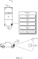
- FIG. 1 illustrates an example environment 100 in which a radar system 102 with one or more an exposed portion of a PCB configured to provide isolation among radar antennas can be implemented.
- the radar system 102 is mounted to, or integrated within, a vehicle 104.
- the radar system 102 is capable of detecting one or more objects 108 that are in proximity to the vehicle 104.
- the vehicle 104 can represent other types of motorized vehicles (e.g ., a motorcycle, a bus, a tractor, a semi-trailer truck, or construction equipment), non-motorized vehicles (e.g., a bicycle), railed vehicles (e.g., a train or a trolley car), watercraft (e.g., a boat or a ship), aircraft (e.g., an airplane or a helicopter), or spacecraft (e.g., satellite).
- manufacturers can mount the radar system 102 to any moving platform, including moving machinery or robotic equipment.
- the radar system 102 is mounted on the front of the vehicle 104 and provides a field-of-view 106 illuminating the one or more objects 108.
- the radar system 102 can project the field-of-view 106 from any exterior surface of the vehicle 104.
- vehicle manufacturers can integrate the radar system 102 into a bumper, side mirror, headlights, rear lights, or any other interior or exterior location where the object 108 requires detection.
- the vehicle 104 includes multiple radar systems 102, such as a first radar system 102 and a second radar system 102 that together provide a larger field-of-view 106.
- vehicle manufacturers can design the locations of the one or more radar systems 102 to provide a particular field-of-view 106 that encompasses a region of interest in which the object 108 may be present.
- Example fields-of-view 106 include a 360-degree field-of-view, one or more 180-degree fields-of-view, one or more 90-degree fields-of-view, and so forth, which can overlap or be combined into a field-of-view 106 of a particular size.
- the object 108 is composed of one or more materials that reflect radar signals. Depending on the application, the object 108 can represent a target of interest. In some cases, the object 108 can be a moving object or a stationary object.
- the stationary objects can be continuous (e.g., a concrete barrier, a guard rail) or discontinuous (e.g., a traffic cone) along a portion of the road.
- the radar system 102 emits electromagnetic radiation by transmitting one or more electromagnetic signals or waveforms via active elements.
- the radar system 102 can detect and track the object 108 by transmitting and receiving one or more radar signals.
- the radar system 102 can transmit electromagnetic signals between 100 and 400 gigahertz (GHz), between 4 and 100 GHz, or between approximately 70 and 80 GHz.
- GHz gigahertz
- the radar system 102 can determine a distance to the object 108 based on the time it takes for the signals to travel from the radar system 102 to the object 108, and from the object 108 back to the radar system 102.
- the radar system 102 can also determine a location of the object 108 in terms of an angle based on the direction of a maximum amplitude echo signal received by the radar system 102.
- the radar system 102 can be part of the vehicle 104.
- the vehicle 104 can also include at least one automotive system that relies on data from the radar system 102, including a driver-assistance system, an autonomous-driving system, or a semi-autonomous-driving system.
- the radar system 102 can include an interface to the at least one automotive system, wherein the antenna 114 can output, via the interface, a signal based on EM energy received by the antenna 114.
- the automotive systems use radar data provided by the radar system 102 to perform a function.
- the driver-assistance system can provide blind-spot monitoring and generate an alert that indicates a potential collision with the object 108 that is detected by the radar system 102.
- the radar data from the radar system 102 indicates when it is safe or unsafe to change lanes.
- the autonomous-driving system may move the vehicle 104 to a particular location on the road while avoiding collisions with the object 108 detected by the radar system 102.
- the radar data provided by the radar system 102 can provide information about a distance to and the location of the object 108 to enable the autonomous-driving system to perform emergency braking, perform a lane change, or adjust the speed of the vehicle 104.
- the radar system 102 includes a transmitter 110 and at least one antenna 114 to transmit electromagnetic signals, and a receiver 112 and the at least one antenna 114 to receive reflected versions of these electromagnetic signals.
- the transmitter 110 includes components for emitting electromagnetic signals.
- the receiver 112 includes one or more components to detect the reflected electromagnetic signals.
- the transmitter 110 and the receiver 112 can be incorporated together on the same integrated circuit (e.g., a transceiver integrated circuit) or separately on different integrated circuits.
- the radar system 102 also includes one or more processors 116 (e.g., an energy processing unit) and computer-readable storage media (CRM) 118.
- the processor 116 can be implemented as a microprocessor or a system-on-chip.
- the processor 116 executes instructions that are stored within the CRM 118.
- the processor 116 can process EM energy received by the antenna 114 and determine a location of the object 108 relative to the radar system 102.
- the processor 116 can also generate radar data for the automotive systems.
- the processor 116 can control, based on processed EM energy from the antenna 114, an autonomous or semi-autonomous driving system of the vehicle 104.
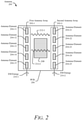
- FIG. 2 illustrates an example antenna 200 with a window 208 for isolation among antenna arrays.
- the antenna 200 includes a first antenna array 202-1 and a second antenna array 202-2 on a PCB 206.
- the PCB 206 includes a metal plating (e.g. , copper alloy) on a top and/or bottom surface.
- the first antenna array 202-1 and the second antenna array 202-2 are configured to emit or receive electromagnetic energy.
- the first antenna array 202-1 and the second antenna array 202-2 can be a transmit antenna array and a receive antenna array, respectively.
- the first antenna array 202-1 and the second antenna array 202-2 can be two transmit antenna arrays or two receive antenna arrays.
- the antenna 200 can include additional antenna arrays 202 with at least one window 208 located between the antenna arrays 202.
- the first antenna array 202-1 and the second antenna array 202-2 include multiple antenna elements 204.
- the antenna arrays 202 can be planar arrays that provide high gain and low loss. Planar arrays are well-suited for vehicle integration due to their small size and depth.
- the antenna elements 204 of the antenna arrays 202 can be slots etched or otherwise formed in the plating material of one surface of the PCB 206 for a substrate-integrated waveguide (SIW) antenna.
- the antenna elements 204 can also include elements of an aperture antenna, a microstrip antenna, or a dipole antenna.
- the antenna arrays 202 can include subarrays of patch elements (e.g. , microstrip patch antenna subarrays) or dipole elements.
- the first antenna array 202-1 includes five antenna elements, including an antenna element 204-11, an antenna element 204-12, an antenna element 204-13, an antenna element 204-14, and an antenna element 204-15.
- the second antenna array 202-2 also includes five antenna elements, including an antenna element 204-21, an antenna element 204-22, an antenna element 204-23, an antenna element 204-24, and an antenna element 204-25.
- the first antenna array 202-1 and/or the second antenna array 202-2 can include fewer or additional antenna elements 204, including a single antenna element 204.
- the first antenna array 202-1 can transmit or receive electromagnetic energy 210-1.
- the metal plating on the surface of the PCB 206 can conduct a portion of the EM energy 212 from the first antenna array 202-1 along the surface of the PCB 206.
- the second antenna array 202-2 can receive the portion of the EM energy 212 conducted by the metal plating.
- the second antenna array 202-2 couples the portion of the EM energy 212 with EM energy 210-2, which is emitted or received by the second antenna array 202-2.
- the first antenna array 202-1 can be a transmit antenna array and the second antenna array 202-2 can be a receive antenna array.
- the first antenna array 202-1 emits the EM energy 210-1
- a relatively large portion of the EM energy 210-1 is radiated perpendicular to the surface of the PCB 206 to illuminate potential targets within the field-of-view 106 of the radar system 102.
- the metal plating also conducts a portion of the EM energy 212 along the surface of the PCB 206.
- the second antenna array 202-2 can couple the portion of the EM energy 212 with the received EM energy 210-2. This coupling can cause a relatively high noise floor (e.g., coupling noise) in the EM energy output by the second antenna array 202-2.
- the at least one window 208 represents an exposed portion of the surface of the PCB 206 without the metal plating. It is also referred to as simply "the window 208" because the portion can be exposed in various ways, not only through etching.
- the window 208 is configured to act as a ground point or ground window on the surface of the PCB 206.
- the window 208 can represent a portion of the metal plating removed or etched away from the surface of the PCB 206.
- the window 208 can represent a portion of the surface of the PCB 206 masked during the metal-plating process for the PCB 206. In this way, the surface of the PCB 206 includes an omitted region of metal plating, wherein the omitted region of metal plating represents the window 208.
- the window 208 is positioned between the first antenna array 202-1 and the second antenna array 202-2.
- the window 208 can generally be positioned anywhere along the coupling path between the first antenna array 202-1 and the second antenna array 202-2.
- Aheight of the window 208 is generally less than a height of the first antenna array 202-1 and/or a height of the second antenna array 202-2.
- a width of the window 208 is effective in delaying a phase of the second part 212-2 of the portion of the EM energy 212 relative to a phase of the first part 212-1 of the portion of the EM energy 212.
- the phase of the first part 212-1 of the portion of the EM energy 212 is delayed due to effects from the dielectric constant of the PCB substrate ( e.g. , slow-wave effect).
- the width of the window 208 can be sufficient to cause the phase of the second part 212-2 of the portion of the EM energy 212 to be delayed by approximately 180 degrees relative to the phase of the first part 212-1 of the portion of the EM energy 212.
- the width of the window 208 can be determined from simulations, empirical analysis, or a combination thereof.
- a height of the window 208 is effective to cause an amount of energy of the second part 212-2 of the portion of the EM energy 212 to be approximately equal to an amount of energy of the first part 212-1 of the portion of the EM energy 212.
- the width and the height of the window 208 can be effective to minimize, or even approximately eliminate, the first part 212-1 against the second part 212-2 of the portion of the EM energy 212.
- the coupling noise at the second antenna array 202-2 can be minimized or approximately eliminated.
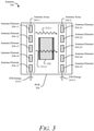
- FIG. 3 illustrates another example antenna 300 with a window 302 for isolation among antenna arrays.
- the antenna 300 is similar to the antenna 200 of FIG. 2 , with many of the same or similar components.
- the antenna 300 includes the first antenna array 202-1 and the second antenna array 202-2 on the PCB 206.
- the first antenna array 202-1 of the antenna 300 can transmit or receive electromagnetic energy 210-1.
- the metal plating on the surface of the PCB 206 can conduct a portion of the EM energy 212 from the first antenna array 202-1 along the surface of the PCB 206.
- the second antenna array 202-2 can receive the portion of the EM energy 212 conducted by the metal plating.
- the second antenna array 202-2 couples the portion of the EM energy 212 with EM energy 210-2, which is emitted or received by the second antenna array 202-2.
- the window 302 of the antenna 300 represents an exposed portion of the surface of the PCB 206 without the metal plating.
- the window 302 can include an irregular surface on opposite sides of the window 302 positioned adjacently to the first antenna array 202-1 and the second antenna array 202-2.
- the irregular surface can include individual peaks and valleys arranged like teeth (e.g., a sawtooth).
- the irregular surface of the window 302 can minimize or avoid edge scattering of the second part 212-2 of the portion of the EM energy 212 that traverses the window 302 at the sides of the window 302.
- the sides of the window 302 can be curved down toward the PCB substrate to minimize edge scattering.
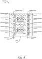
- FIG. 4 illustrates an example antenna 400 with multiple windows 208 for isolation among antenna arrays.
- the antenna 400 is similar to the antenna 200 of FIG. 2 , with many of the same or similar components.
- the antenna 400 includes the first antenna array 202-1 and the second antenna array 202-2 on the PCB 206.
- the first antenna array 202-1 of the antenna 300 can transmit or receive electromagnetic energy 210-1.
- the metal plating on the surface of the PCB 206 can conduct a portion of the EM energy 212 from the first antenna array 202-1 along the surface of the PCB 206.
- the second antenna array 202-2 can receive the portion of the EM energy 212 conducted by the metal plating.
- the second antenna array 202-2 couples the portion of the EM energy 212 with EM energy 210-2, which is emitted or received by the second antenna array 202-2.
- the antenna 400 includes a first window 208-1 and a second window 208-2.
- the antenna 400 can include additional windows 208. Similar to the window 208 of FIG. 2 , the first window 208-1 and the second window 208-2 of the antenna 400 represents an exposed portion of the surface of the PCB 206 without the metal plating.
- the first window 208-1 and the second window 208-2 are positioned between the first antenna array 202-1 and the second antenna array 202-2.
- the first window 208-1 and the second window 208-2 can be positioned generally anywhere along the coupling path between first antenna array 202-1 and the second antenna array 202-2.
- a width of the first window 208-1 and the second window 208-2 is effective to delay a phase of the second parts 212-2 and 212-4 of the portion of the EM energy 212 relative to a phase of the first parts 212-1 and 212-3 of the portion of the EM energy 212.
- the width of the first window 208-1 is generally equal or approximately equal to the width of the second window 208-2.
- a collective height of the first window 208-1 and the second window 208-2 is effective to cause an amount of energy of the second parts 212-2 and 212-4 of the portion of the EM energy 212 to be approximately equal to an amount of energy of the first parts 212-1 and 212-3 of the portion of the EM energy 212.
- the width and the collective height of the first window 208-1 and the second window 208-2 can be effective to minimize, or even cancel, the first parts 212-1 and 212-3 against the second parts 212-2 and 212-4 of the portion of the EM energy 212.
- the first window 208-1 and the second window 208-2 have a rectangular shape or an approximately rectangular shape.
- the first antenna array 202-1 is positioned adjacently to a first side of the first window 208-1 and the second window 208-2 and the second antenna array 202-2 is positioned adjacently to a second side of the first window 208-1 and the second window 208-2 opposed the first side.
- the window 208 of FIG. 2 , the window 302 of FIG. 3 , the first window 208-1 of FIG. 4 , and the second window 208-2 of FIG. 4 can have a different shape.
- a width and height of the window(s) can be determined using simulations or empirical analysis to minimize or cancel the first part 212-1 of the portion of the EM energy 212 against the second part 212-2 of the portion of the EM energy 212.
- FIG. 5 depicts an example method 500 of an exposed portion of a PCB configured to provide isolation among radar antennas.
- Method 500 is shown as sets of operations (or acts) performed, but not necessarily limited to the order or combinations in which the operations are shown herein. Further, any of one or more of the operations may be repeated, combined, or reorganized to provide other methods.
- reference may be made to the environment 100 of FIG. 1 and entities detailed in FIGs. 1 through 4 , reference to which is made for example only. The techniques are not limited to performance by one entity or multiple entities.
- a first antenna and a second antenna are added to a surface of a PCB.
- the first antenna array 202-1 and a second antenna array 202-2 are added to a surface of the PCB 206.
- a metal plating is applied to the surface of the PCB.
- the metal plating is configured to conduct a portion of the EM energy from the first antenna on the surface of the PCB.
- a metal plating is applied to the surface of the PCB 206.
- the metal plating conducts a portion of the EM energy 212 from the first antenna array 202-1 on the surface of the PCB 206.
- the second antenna array 202 is configured to receive the portion of the EM energy 212 and is coupled with the EM energy 210-2.
- an exposed portion of the surface of the PCB is provided.
- the exposed portion is positioned between the first antenna and the second antenna.
- a window 208 is provided on the surface of the PCB 206 and represents an exposed portion of the surface of the PCB 206.
- the window 208 is positioned between the first antenna array 202-1 and the second antenna array 202-2.
- a width of the exposed portion is set.
- the width is effective to delay a phase of a first part of the portion of the EM energy that traverses the exposed portion relative to a phase of a second part of the portion of the EM energy that does not traverse the exposed portion.
- the width of the window 208 is set.
- the width of the window 208 is effective to delay a phase of the second part 212-2 of the portion of the EM energy that traverses the window 208 relative to the phase of the first part 212-1 of the portion of the EM energy that does not traverse the window 208.
- a height of the exposed portion is set.
- the height is effective to cause an amount of energy of the first part of the portion of the EM energy to be approximately equal to an amount of energy of the second part of the portion of the EM energy.
- the height of the window 208 is set.
- the height of the window 208 is effective to cause the amount of energy of the first part 212-1 of the portion of the EM energy to be approximately equal to the amount of energy of the second part 212-2 of the portion of the EM energy.
Landscapes
- Engineering & Computer Science (AREA)
- Radar, Positioning & Navigation (AREA)
- Remote Sensing (AREA)
- Physics & Mathematics (AREA)
- Computer Networks & Wireless Communication (AREA)
- General Physics & Mathematics (AREA)
- Computer Security & Cryptography (AREA)
- Electromagnetism (AREA)
- Radar Systems Or Details Thereof (AREA)
- Variable-Direction Aerials And Aerial Arrays (AREA)
- Details Of Aerials (AREA)
Applications Claiming Priority (1)
| Application Number | Priority Date | Filing Date | Title |
|---|---|---|---|
| US16/995,748 US11196153B1 (en) | 2020-08-17 | 2020-08-17 | Exposed portion of a printed circuit board (PCB) configured to provide isolation among radar antennas |
Publications (2)
| Publication Number | Publication Date |
|---|---|
| EP3958010A2 true EP3958010A2 (de) | 2022-02-23 |
| EP3958010A3 EP3958010A3 (de) | 2022-03-23 |
Family
ID=77226646
Family Applications (1)
| Application Number | Title | Priority Date | Filing Date |
|---|---|---|---|
| EP21189771.5A Pending EP3958010A3 (de) | 2020-08-17 | 2021-08-05 | Freiliegender teil einer leiterplatte zur isolierung zwischen radarantennen |
Country Status (3)
| Country | Link |
|---|---|
| US (2) | US11196153B1 (de) |
| EP (1) | EP3958010A3 (de) |
| CN (1) | CN114076947A (de) |
Families Citing this family (3)
| Publication number | Priority date | Publication date | Assignee | Title |
|---|---|---|---|---|
| US11196153B1 (en) * | 2020-08-17 | 2021-12-07 | Aptiv Technologies Limited | Exposed portion of a printed circuit board (PCB) configured to provide isolation among radar antennas |
| US12408261B2 (en) | 2023-04-24 | 2025-09-02 | Aptiv Technologies AG | Isolation slots for an antenna and printed circuit board interface |
| WO2025195694A1 (de) * | 2024-03-20 | 2025-09-25 | Robert Bosch Gmbh | Radarsensor mit entkopplungsmitteln für oberflächenwellen |
Family Cites Families (16)
| Publication number | Priority date | Publication date | Assignee | Title |
|---|---|---|---|---|
| US5047787A (en) * | 1989-05-01 | 1991-09-10 | Motorola, Inc. | Coupling cancellation for antenna arrays |
| JPH09270633A (ja) * | 1996-03-29 | 1997-10-14 | Hitachi Ltd | Temスロットアレイアンテナ |
| US6583760B2 (en) * | 1998-12-17 | 2003-06-24 | Metawave Communications Corporation | Dual mode switched beam antenna |
| US6198434B1 (en) * | 1998-12-17 | 2001-03-06 | Metawave Communications Corporation | Dual mode switched beam antenna |
| IL207125A0 (en) * | 2010-07-21 | 2011-04-28 | Elta Systems Ltd | Deployable antenna array |
| JP6095444B2 (ja) * | 2013-03-29 | 2017-03-15 | 富士通テン株式会社 | アンテナ装置およびレーダ装置 |
| US10833401B2 (en) * | 2015-11-25 | 2020-11-10 | Commscope Technologies Llc | Phased array antennas having decoupling units |
| US10333209B2 (en) * | 2016-07-19 | 2019-06-25 | Toyota Motor Engineering & Manufacturing North America, Inc. | Compact volume scan end-fire radar for vehicle applications |
| CN106207457B (zh) * | 2016-09-21 | 2019-03-29 | 广东通宇通讯股份有限公司 | 天线、mimo天线及用于降低天线互耦能量的隔离条 |
| US9917355B1 (en) * | 2016-10-06 | 2018-03-13 | Toyota Motor Engineering & Manufacturing North America, Inc. | Wide field of view volumetric scan automotive radar with end-fire antenna |
| WO2018105513A1 (en) * | 2016-12-06 | 2018-06-14 | Nidec Corporation | Waveguide device module and microwave module |
| DE102018115610A1 (de) * | 2017-06-30 | 2019-01-03 | Nidec Corporation | Wellenleitervorrichtungsmodul, Mikrowellenmodul, Radarvorrichtung und Radarsystem |
| US11050167B2 (en) * | 2018-04-19 | 2021-06-29 | Samsung Electronics Co., Ltd. | Antenna array and operation method of antenna array |
| CN109638458B (zh) * | 2018-12-19 | 2022-02-11 | 新华三技术有限公司成都分公司 | 天线隔离度调节系统 |
| US11544691B2 (en) * | 2019-04-30 | 2023-01-03 | Vayyar Imaging Ltd. | Radar based sensing for retail applications |
| US11196153B1 (en) * | 2020-08-17 | 2021-12-07 | Aptiv Technologies Limited | Exposed portion of a printed circuit board (PCB) configured to provide isolation among radar antennas |
-
2020
- 2020-08-17 US US16/995,748 patent/US11196153B1/en active Active
-
2021
- 2021-08-05 EP EP21189771.5A patent/EP3958010A3/de active Pending
- 2021-08-16 CN CN202110939208.XA patent/CN114076947A/zh active Pending
- 2021-11-01 US US17/516,575 patent/US11588228B2/en active Active
Also Published As
| Publication number | Publication date |
|---|---|
| CN114076947A (zh) | 2022-02-22 |
| US11196153B1 (en) | 2021-12-07 |
| US20220059930A1 (en) | 2022-02-24 |
| US11588228B2 (en) | 2023-02-21 |
| EP3958010A3 (de) | 2022-03-23 |
Similar Documents
| Publication | Publication Date | Title |
|---|---|---|
| US11588228B2 (en) | Exposed portion of a printed circuit board (PCB) configured to provide isolation among radar antennas | |
| US11714180B2 (en) | Radar system to detect angles in bistatic and monostatic scenarios | |
| US12153157B2 (en) | Radar system with paired one-dimensional and two-dimensional antenna arrays | |
| US11749883B2 (en) | Waveguide with radiation slots and parasitic elements for asymmetrical coverage | |
| US11644565B2 (en) | Radar system with sparse primary array and dense auxiliary array | |
| CN112654888A (zh) | 电子设备、电子设备的控制方法、以及电子设备的控制程序 | |
| EP4099500A1 (de) | Wellenförmige grundruktur für gruppenantennen | |
| WO2022113766A1 (ja) | 電子機器、電子機器の制御方法、及びプログラム | |
| CN116547183A (zh) | 电子设备、电子设备的控制方法以及程序 | |
| EP4016732A1 (de) | Wellenleiter mit schlitzgespeisten dipolelementen | |
| US20240154289A1 (en) | Waveguide With A Zigzag For Suppressing Grating Lobes | |
| US11502420B2 (en) | Twin line fed dipole array antenna | |
| US11721905B2 (en) | Waveguide with a beam-forming feature with radiation slots | |
| WO2022209834A1 (ja) | 電子機器 | |
| US12614839B2 (en) | Waveguide with radiation slots and parasitic elements for asymmetrical coverage | |
| US12456816B2 (en) | Waveguide with slot antennas and reflectors |
Legal Events
| Date | Code | Title | Description |
|---|---|---|---|
| PUAI | Public reference made under article 153(3) epc to a published international application that has entered the european phase |
Free format text: ORIGINAL CODE: 0009012 |
|
| STAA | Information on the status of an ep patent application or granted ep patent |
Free format text: STATUS: THE APPLICATION HAS BEEN PUBLISHED |
|
| REG | Reference to a national code |
Ref country code: DE Ref legal event code: R079 Free format text: PREVIOUS MAIN CLASS: G01S0007030000 Ipc: H01Q0001520000 |
|
| PUAL | Search report despatched |
Free format text: ORIGINAL CODE: 0009013 |
|
| AK | Designated contracting states |
Kind code of ref document: A2 Designated state(s): AL AT BE BG CH CY CZ DE DK EE ES FI FR GB GR HR HU IE IS IT LI LT LU LV MC MK MT NL NO PL PT RO RS SE SI SK SM TR |
|
| AK | Designated contracting states |
Kind code of ref document: A3 Designated state(s): AL AT BE BG CH CY CZ DE DK EE ES FI FR GB GR HR HU IE IS IT LI LT LU LV MC MK MT NL NO PL PT RO RS SE SI SK SM TR |
|
| RIC1 | Information provided on ipc code assigned before grant |
Ipc: H01Q 21/08 20060101ALI20220215BHEP Ipc: G01S 13/93 20200101ALI20220215BHEP Ipc: G01S 7/03 20060101ALI20220215BHEP Ipc: H01Q 1/52 20060101AFI20220215BHEP |
|
| STAA | Information on the status of an ep patent application or granted ep patent |
Free format text: STATUS: REQUEST FOR EXAMINATION WAS MADE |
|
| 17P | Request for examination filed |
Effective date: 20220922 |
|
| RBV | Designated contracting states (corrected) |
Designated state(s): AL AT BE BG CH CY CZ DE DK EE ES FI FR GB GR HR HU IE IS IT LI LT LU LV MC MK MT NL NO PL PT RO RS SE SI SK SM TR |
|
| RAP3 | Party data changed (applicant data changed or rights of an application transferred) |
Owner name: APTIV TECHNOLOGIES LIMITED |
|
| STAA | Information on the status of an ep patent application or granted ep patent |
Free format text: STATUS: EXAMINATION IS IN PROGRESS |
|
| 17Q | First examination report despatched |
Effective date: 20230926 |
|
| RAP1 | Party data changed (applicant data changed or rights of an application transferred) |
Owner name: APTIV TECHNOLOGIES AG |
|
| RAP3 | Party data changed (applicant data changed or rights of an application transferred) |
Owner name: APTIV TECHNOLOGIES AG |