EP3955449A1 - Control device and converter - Google Patents
Control device and converter Download PDFInfo
- Publication number
- EP3955449A1 EP3955449A1 EP21189719.4A EP21189719A EP3955449A1 EP 3955449 A1 EP3955449 A1 EP 3955449A1 EP 21189719 A EP21189719 A EP 21189719A EP 3955449 A1 EP3955449 A1 EP 3955449A1
- Authority
- EP
- European Patent Office
- Prior art keywords
- model
- converter
- power supply
- block
- control
- Prior art date
- Legal status (The legal status is an assumption and is not a legal conclusion. Google has not performed a legal analysis and makes no representation as to the accuracy of the status listed.)
- Withdrawn
Links
Images





Classifications
-
- H—ELECTRICITY
- H02—GENERATION; CONVERSION OR DISTRIBUTION OF ELECTRIC POWER
- H02M—APPARATUS FOR CONVERSION BETWEEN AC AND AC, BETWEEN AC AND DC, OR BETWEEN DC AND DC, AND FOR USE WITH MAINS OR SIMILAR POWER SUPPLY SYSTEMS; CONVERSION OF DC OR AC INPUT POWER INTO SURGE OUTPUT POWER; CONTROL OR REGULATION THEREOF
- H02M3/00—Conversion of DC power input into DC power output
- H02M3/02—Conversion of DC power input into DC power output without intermediate conversion into AC
- H02M3/04—Conversion of DC power input into DC power output without intermediate conversion into AC by static converters
- H02M3/10—Conversion of DC power input into DC power output without intermediate conversion into AC by static converters using discharge tubes with control electrode or semiconductor devices with control electrode
- H02M3/145—Conversion of DC power input into DC power output without intermediate conversion into AC by static converters using discharge tubes with control electrode or semiconductor devices with control electrode using devices of a triode or transistor type requiring continuous application of a control signal
- H02M3/155—Conversion of DC power input into DC power output without intermediate conversion into AC by static converters using discharge tubes with control electrode or semiconductor devices with control electrode using devices of a triode or transistor type requiring continuous application of a control signal using semiconductor devices only
- H02M3/156—Conversion of DC power input into DC power output without intermediate conversion into AC by static converters using discharge tubes with control electrode or semiconductor devices with control electrode using devices of a triode or transistor type requiring continuous application of a control signal using semiconductor devices only with automatic control of output voltage or current, e.g. switching regulators
-
- G—PHYSICS
- G06—COMPUTING OR CALCULATING; COUNTING
- G06N—COMPUTING ARRANGEMENTS BASED ON SPECIFIC COMPUTATIONAL MODELS
- G06N3/00—Computing arrangements based on biological models
- G06N3/02—Neural networks
- G06N3/08—Learning methods
-
- G—PHYSICS
- G06—COMPUTING OR CALCULATING; COUNTING
- G06N—COMPUTING ARRANGEMENTS BASED ON SPECIFIC COMPUTATIONAL MODELS
- G06N3/00—Computing arrangements based on biological models
- G06N3/02—Neural networks
- G06N3/04—Architecture, e.g. interconnection topology
- G06N3/044—Recurrent networks, e.g. Hopfield networks
- G06N3/0442—Recurrent networks, e.g. Hopfield networks characterised by memory or gating, e.g. long short-term memory [LSTM] or gated recurrent units [GRU]
-
- G—PHYSICS
- G06—COMPUTING OR CALCULATING; COUNTING
- G06N—COMPUTING ARRANGEMENTS BASED ON SPECIFIC COMPUTATIONAL MODELS
- G06N3/00—Computing arrangements based on biological models
- G06N3/02—Neural networks
- G06N3/08—Learning methods
- G06N3/09—Supervised learning
-
- H—ELECTRICITY
- H02—GENERATION; CONVERSION OR DISTRIBUTION OF ELECTRIC POWER
- H02M—APPARATUS FOR CONVERSION BETWEEN AC AND AC, BETWEEN AC AND DC, OR BETWEEN DC AND DC, AND FOR USE WITH MAINS OR SIMILAR POWER SUPPLY SYSTEMS; CONVERSION OF DC OR AC INPUT POWER INTO SURGE OUTPUT POWER; CONTROL OR REGULATION THEREOF
- H02M1/00—Details of apparatus for conversion
- H02M1/0045—Converters combining the concepts of switch-mode regulation and linear regulation, e.g. linear pre-regulator to switching converter, linear and switching converter in parallel, same converter or same transistor operating either in linear or switching mode
-
- H—ELECTRICITY
- H02—GENERATION; CONVERSION OR DISTRIBUTION OF ELECTRIC POWER
- H02M—APPARATUS FOR CONVERSION BETWEEN AC AND AC, BETWEEN AC AND DC, OR BETWEEN DC AND DC, AND FOR USE WITH MAINS OR SIMILAR POWER SUPPLY SYSTEMS; CONVERSION OF DC OR AC INPUT POWER INTO SURGE OUTPUT POWER; CONTROL OR REGULATION THEREOF
- H02M3/00—Conversion of DC power input into DC power output
- H02M3/02—Conversion of DC power input into DC power output without intermediate conversion into AC
- H02M3/04—Conversion of DC power input into DC power output without intermediate conversion into AC by static converters
- H02M3/10—Conversion of DC power input into DC power output without intermediate conversion into AC by static converters using discharge tubes with control electrode or semiconductor devices with control electrode
- H02M3/145—Conversion of DC power input into DC power output without intermediate conversion into AC by static converters using discharge tubes with control electrode or semiconductor devices with control electrode using devices of a triode or transistor type requiring continuous application of a control signal
- H02M3/155—Conversion of DC power input into DC power output without intermediate conversion into AC by static converters using discharge tubes with control electrode or semiconductor devices with control electrode using devices of a triode or transistor type requiring continuous application of a control signal using semiconductor devices only
- H02M3/156—Conversion of DC power input into DC power output without intermediate conversion into AC by static converters using discharge tubes with control electrode or semiconductor devices with control electrode using devices of a triode or transistor type requiring continuous application of a control signal using semiconductor devices only with automatic control of output voltage or current, e.g. switching regulators
- H02M3/157—Conversion of DC power input into DC power output without intermediate conversion into AC by static converters using discharge tubes with control electrode or semiconductor devices with control electrode using devices of a triode or transistor type requiring continuous application of a control signal using semiconductor devices only with automatic control of output voltage or current, e.g. switching regulators with digital control
-
- H—ELECTRICITY
- H02—GENERATION; CONVERSION OR DISTRIBUTION OF ELECTRIC POWER
- H02M—APPARATUS FOR CONVERSION BETWEEN AC AND AC, BETWEEN AC AND DC, OR BETWEEN DC AND DC, AND FOR USE WITH MAINS OR SIMILAR POWER SUPPLY SYSTEMS; CONVERSION OF DC OR AC INPUT POWER INTO SURGE OUTPUT POWER; CONTROL OR REGULATION THEREOF
- H02M3/00—Conversion of DC power input into DC power output
- H02M3/02—Conversion of DC power input into DC power output without intermediate conversion into AC
- H02M3/04—Conversion of DC power input into DC power output without intermediate conversion into AC by static converters
- H02M3/10—Conversion of DC power input into DC power output without intermediate conversion into AC by static converters using discharge tubes with control electrode or semiconductor devices with control electrode
- H02M3/145—Conversion of DC power input into DC power output without intermediate conversion into AC by static converters using discharge tubes with control electrode or semiconductor devices with control electrode using devices of a triode or transistor type requiring continuous application of a control signal
- H02M3/155—Conversion of DC power input into DC power output without intermediate conversion into AC by static converters using discharge tubes with control electrode or semiconductor devices with control electrode using devices of a triode or transistor type requiring continuous application of a control signal using semiconductor devices only
- H02M3/156—Conversion of DC power input into DC power output without intermediate conversion into AC by static converters using discharge tubes with control electrode or semiconductor devices with control electrode using devices of a triode or transistor type requiring continuous application of a control signal using semiconductor devices only with automatic control of output voltage or current, e.g. switching regulators
- H02M3/158—Conversion of DC power input into DC power output without intermediate conversion into AC by static converters using discharge tubes with control electrode or semiconductor devices with control electrode using devices of a triode or transistor type requiring continuous application of a control signal using semiconductor devices only with automatic control of output voltage or current, e.g. switching regulators including plural semiconductor devices as final control devices for a single load
-
- H—ELECTRICITY
- H02—GENERATION; CONVERSION OR DISTRIBUTION OF ELECTRIC POWER
- H02M—APPARATUS FOR CONVERSION BETWEEN AC AND AC, BETWEEN AC AND DC, OR BETWEEN DC AND DC, AND FOR USE WITH MAINS OR SIMILAR POWER SUPPLY SYSTEMS; CONVERSION OF DC OR AC INPUT POWER INTO SURGE OUTPUT POWER; CONTROL OR REGULATION THEREOF
- H02M7/00—Conversion of AC power input into DC power output; Conversion of DC power input into AC power output
- H02M7/02—Conversion of AC power input into DC power output without possibility of reversal
- H02M7/04—Conversion of AC power input into DC power output without possibility of reversal by static converters
- H02M7/12—Conversion of AC power input into DC power output without possibility of reversal by static converters using discharge tubes with control electrode or semiconductor devices with control electrode
- H02M7/21—Conversion of AC power input into DC power output without possibility of reversal by static converters using discharge tubes with control electrode or semiconductor devices with control electrode using devices of a triode or transistor type requiring continuous application of a control signal
- H02M7/217—Conversion of AC power input into DC power output without possibility of reversal by static converters using discharge tubes with control electrode or semiconductor devices with control electrode using devices of a triode or transistor type requiring continuous application of a control signal using semiconductor devices only
Definitions
- the present disclosure relates to a control device for controlling a converter, and a converter.
- DC/DC converters and AC/DC converters that respectively convert input DC and AC power into DC power of a predetermined voltage by using pulse width modulation (PWM), and supply the converted DC power are known in the related art.
- PWM pulse width modulation
- a PID control in which a feedback-control using a deviation from a target value and integral and derivative of the deviation is performed, has sometimes been used.
- a DC/DC converter that switches between a PID control and a fuzzy control by an artificial intelligence neural network is known.
- a RegimeCast method is also known in the related art.
- long-term event prediction is realized by discovering features from among large-scale data streams such as sensor data and automatically recognizing potential time-series patterns, that is, regimes, by extending the concept of "regime shift" in a natural ecosystem model to express time-series event data as an adaptive nonlinear dynamic system.
- FIG. 1 is a time chart for explaining RegimeCast.
- a latest time frame Xc from a past time t m to a current time tc actual data of possible regimes are indicated by different thin lines.
- Future data can be predicted by selecting an optimal model for the actual data from a plurality of models indicated by different thick lines and applying the selected model to a time frame X F from the current time t c to a future time ts. For example, events from the time t c to the time ts in the future time frame X F can be predicted based on an event stream of the latest time frame X C .
- the PID control performs control so as to follow the target value by adjusting the deviation from the target value and the integration and differentiation of the deviation, it is difficult to respond to all controls.
- Some embodiments of the present disclosure provide a control device and a converter capable of quickly converging an output voltage to a target value even in the case of an unexpected fluctuation in the converter, and furthermore, reducing overshoot, ringing, noise, loss, or the like that may occur due to the fluctuation.
- a control device controls an output voltage of a converter.
- the control device includes: a neural network configured to generate a control signal for controlling a power supply block based on a detection signal from an output stage of the power supply block that supplies power to a load of the converter; a model generator configured to generate a model of a nonlinear dynamic system by machine-learning from the detection signal; a model storage configured to store the model generated by the model generator; and a model switch configured to switch to a model, which is selected from models stored in the model storage and is optimal for a latest detection signal, and provide the switched model to the neural network, wherein the neural network generates the control signal based on a future output voltage predicted by using the model provided by the model switch.
- the control device may further include a waveform generator configured to generate a waveform for driving the power supply block based on the control signal supplied from the neural network.
- the converter may be a DC/DC converter or an AC/DC converter.
- a converter includes a power supply block configured to supply power to a load, and a control block configured to control the power supply block.
- the control block includes: a neural network that generates a control signal for controlling the power supply block based on a detection signal from an output stage of the power supply block; a model generator that generates a model of a nonlinear dynamic system by machine-learning from the detection signal; a model storage that stores the model generated by the model generator; and a model switch that switches to a model which is selected from models stored in the model storage and is optimal for a latest detection signal, and provides the switched model to the neural network, wherein the neural network generates the control signal based on a future output voltage predicted by using the model provided by the model switch.
- the control block may convert the control signal, which is digital data, supplied from the neural network into an analog signal, and supply the analog signal to the power supply block.
- the power supply block may include a transistor and a diode, which are connected in series between a power supply line and a ground line, and the transistor may be driven based on the control signal from the control block to output a current from a connection node between the transistor and the diode.
- the neural network may control the transistor to operate in an active region.
- the power supply block may include a first transistor and a second transistor, which are connected in series between a power supply line and a ground line, and the first transistor and the second transistor may be driven based on the control signal from the control block to output a current from a connection node between the first transistor and the second transistor.
- the neural network may control at least one of the first transistor and the second transistor to operate in an active region.
- the control block and the power supply block may be galvanically insulated from each other.
- the converter may constitute a DC/DC converter or an AC/DC converter.
- a control device realizes RegimeCast known in the related art by artificial intelligence by a neural network and controls a power supply block of a converter to supply an output voltage of a target value.
- the control device may be included as a control block in the converter, or may form the converter together with the power supply block.
- a DC/DC converter and an AC/DC converter are collectively referred to as a converter.
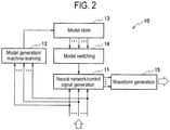
- FIG. 2 is a diagram showing a schematic configuration of a control device according to a first embodiment.
- a control device 10 includes a neural network 11 that generates a control signal for controlling a power supply block in a converter.
- the neural network 11 generates the control signal for controlling the power supply block (not shown) by using a model of a nonlinear dynamic system, based on a detection signal provided from the power supply block.
- the detection signal is input to the neural network 11, as time-series data converted into digital data by an A/D converter (not shown).
- the detection signal may be at least one or more of an output voltage value, an output current value, an input voltage value, an inductor current value, a capacitor current value, and the like of the power supply block.
- the control signal generated by using the model is output as digital data from the neural network 11.
- the neural network 11 may be an appropriate type of neural network such as a spiking neural network, a recurrent neural network, a convolutional neural network, a fuzzy neural network, and the like.
- the control device 10 includes a model generator 12 that generates a model by machine-learning from the detection signal supplied from the power supply block.
- the model generator 12 learns the detection signal as learning data to generate a model of a nonlinear dynamic system.
- the model generator 12 may determine parameters of the model of the nonlinear dynamic system.
- the same detection signal input to the neural network 11 is input to the model generator 12.
- the detection signal is time-series data converted into a digital signal by an A/D converter (not shown).
- the control device 10 includes a model storage 13 that stores the model generated by the model generator 12. Data of the model generated by the model generator 12 are supplied to the model storage 13.
- the data of the model may be, for example, parameters of the model of the nonlinear dynamic system.
- the model storage 13 may be configured by a nonvolatile memory.
- the control device 10 includes a model switch 14 that switches the model stored in the model storage 13 and provides it to the neural network 11.
- the same detection signal input to the neural network 11 is input to the model switch 14 through a signal line (not shown).
- the detection signal is time-series data converted into a digital signal by an A/D converter (not shown).
- the model switch 14 Based on the time-series data of the input detection signal, the model switch 14 adaptively switches to an optimal model for the time-series data in real time from among a plurality of models stored in the model storage 13, and provides the optimal model to the neural network 11.
- the model may be given by parameters of the model of the nonlinear dynamic system.
- the neural network 11 uses the model provided from the model switch 14 to generate the control signal for controlling the power supply block based on the time-series data of the detection signal.
- the neural network 11 can predict future time-series data by expressing the time-series data as an adaptive nonlinear dynamic system by the concept of regime shift, and can generate the control signal that controls the power supply block so as to perform quick convergence to a target value.
- parameters of the nonlinear dynamic system of the model may be provided to the neural network 11.
- the neural network outputs the control signal as digital data.
- the control device 10 includes a waveform generator 15 that converts the control signal, which is digital data supplied from the neural network 11, into an analog signal waveform and provides the analog signal waveform to the power supply block.
- the waveform generator 15 may be configured by a D/A converter.
- the waveform generator 15 generates a waveform necessary for controlling on/off of a single transistor serving as a corresponding switching element in the power supply block.
- the power supply block may include a single transistor as a switching element even when the power supply block constitutes a DC/DC converter or a single-phase AC/DC converter.
- the model generator 12 generates various models from a piece of time-series data based on the detection signal
- the model storage 13 stores the generated models
- the model switch 14 selects the optimal model in real time from the models stored in the model storage 13 based on the time-series data of the detection signal.
- the neural network 11 uses the model provided from the model switch 14 to generate a predicted value that predicts a future output voltage of the power supply block based on the time-series data of the detection signal, generates an appropriate control signal based on this predicted value so that the predicted value converges to the target value, and provides the generated control signal to the power supply block through the waveform generator 15.
- an appropriate control signal can be generated at a timing when control is required, based on the time-series data of the detection signal. Accordingly, the output voltage of the power supply block 30 can be quickly converged to the target value even in the case of an unexpected fluctuation, and furthermore, overshoot, ringing, noise, loss, and the like that may occur due to the fluctuation can be reduced.
- control device 10 may be provided alone to control the power supply block, or may form a DC/DC converter or a single-phase AC/DC converter together with the power supply block.
- control device 10 may be configured as a single device by a semiconductor integrated circuit, or the neural network 11, the model generator 12, the model storage 13, the model switch 14, and the waveform generator 15 may be configured by individual devices.
- the neural network 11, the model generator 12, and the model switch 14 may be configured as logic blocks in a single device.
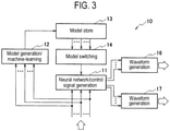
- FIG. 3 is a diagram showing a schematic configuration of a control device according to a second embodiment.
- the control device according to the second embodiment and the control device 10 according to the first embodiment shown in FIG. 2 are common in that they both include: the neural network 11 that generates the control signal for controlling the power supply block in the converter; the model generator 12 that generates the model by machine-learning from the detection signal supplied from the power supply block; the model storage 13 that stores the model generated by the model generator 12; and the model switch 14 that switches the model stored in the model storage 13 and provides it to the neural network 11.
- elements common to the control device 10 according to the first embodiment are denoted by the same reference numerals as in the first embodiment.
- the control device 10 according to the second embodiment is different from the control device 10 according to the first embodiment in that the latter has the single waveform generator 15 while the former has two waveform generators, i.e., first and second waveform generators 16 and 17.
- Control signals based on digital data are supplied from the neural network 11 to the first waveform generator 16 and the second waveform generator 17, respectively.
- the first waveform generator 16 and the second waveform generator 17 may be configured by D/A converters, respectively, like the waveform generator 15 of the control device 10 according to the first embodiment.
- the first waveform generator 16 and the second waveform generator 17 respectively generate waveforms required for individually controlling on/off of two transistors serving as corresponding switching elements in the power supply block based on the control signals from the neural network 11.
- the power supply block may include two transistors as switching elements even when the power supply block constitutes a DC/DC converter, a single-phase AC/DC converter, or a two-phase AC/DC converter.
- the neural network 11 can use an optimal model in real time to generate a predicted value that predicts a future output voltage of the power supply block from time-series data of the detection signal, can generate appropriate control signals based on this predicted value so that the predicted value converges to a target value, and can provide the control signals to the power supply block through the first waveform generator 16 and the second waveform generator 17.
- the control device 10 can generate the appropriate control signals at a timing when a control is required, based on the time-series data of the control signals, and can individually control the two transistors included in the power supply block through the first waveform generator 16 and the second waveform generator 17. For this reason, the output voltage of the power supply block can be quickly converged to the target value even in the case of an unexpected fluctuation, and furthermore, overshoot, ringing, noise, and loss that may occur due to the fluctuation can be reduced.
- the control device 10 according to the second embodiment may be provided alone to control the power supply block, or may form a DC/DC converter, a single-phase AC/DC converter, or a two-phase AC/DC converter together with the power supply block. Further, like the control device 10 according to the first embodiment, the control device 10 according to the second embodiment may be configured as a single device by a semiconductor integrated circuit, or the neural network 11, the model generator 12, the model storage 13, the model switch 14, and the first and second waveform generators 16 and 17 may be configured by individual devices. The neural network 11, the model generator 12, and the model switch 14 may be configured as logic blocks in a single device.
- the control device 10 includes the first waveform generator 16 and the second waveform generator 17 to generate waveforms of the control signals that individually control on/off of the two transistors serving as the corresponding switching elements in the power supply block, but may include three waveform generators when it is necessary to individually control on/off of three transistors serving as corresponding switching elements in the power supply block in a similar manner. Also in this case, the three waveform generators generate waveforms required to individually control on/off of the three transistors serving as the corresponding switching elements in the power supply block based on control signals from the neural network 11.
- the power supply block may include the three transistors as the switching elements even when the power supply block constitutes a DC/DC converter, a single-phase AC/DC converter, a two-phase AC/DC converter, or a three-phase AC/DC converter.
- the control device 10 according to the second embodiment may have four or more waveform generators.
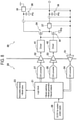
- FIG. 4 is a diagram showing a schematic configuration of a DC/DC converter according to a third embodiment.
- the DC/DC converter constitutes an asynchronous rectification type step-down DC/DC converter.
- the DC/DC converter includes a control block 20 and a power supply block 30, which is driven based on a control signal supplied from the control block 20.
- the control block 20 has a logic block 21 having functions of model generation, model switching, and a neural network, and a nonvolatile memory 23 that stores models.
- control block 20 has an A/D converter 24 configured to convert a detection signal as an analog signal provided from the power supply block 30 into digital data and provide it to the logic block 21, and a D/A converter 25 configured to convert a control signal as the digital data output from the logic block 21 into an analog signal and supply it to the power supply block 30.
- control block 20 has a DC/DC converter 26 for system power supply that supplies power to the control block 20.
- FIG. 5 is a diagram showing a schematic configuration of the control block 20 of the DC/DC converter according to the third embodiment.
- the logic block 21 has a neural network 11 that generates a control signal for controlling the power supply block 30, a model generator 12 that generates a model by machine-learning from a detection signal supplied from the power supply block 30, and a model switch 14 that selects an optimal model based on the detection signal supplied from the power supply block 30.
- elements of the logic block 21, which is common with the control device 10 according to the first embodiment, are denoted by the corresponding reference numerals.
- the nonvolatile memory 23 and the D/A converter 25 correspond to the model storage 13 and the waveform generator 15, respectively, of the control device 10 according to the first embodiment.
- the neural network 11 uses a model of a nonlinear dynamic system to generate the control signal for controlling the power supply block based on the detection signal provided from the power supply block 30.
- the detection signal is input as time-series data converted into a digital signal by the A/D converter 24.
- the detection signal may be at least one or more of an output voltage value, an output current value, an input voltage value, an inductor current value, a capacitor current value, and the like of the power supply block 30.
- the control signal generated by using the model is output as digital data from the neural network 11.
- the neural network 11 may be an appropriate type of neural network such as a spiking neural network, a recurrent neural network, a convolutional neural network, or a fuzzy neural network.
- the model generator 12 learns the detection signal as learning data and generates a model of a nonlinear dynamic system. For example, the model generator 12 may determine parameters of the model of the nonlinear dynamic system.
- the same detection signal input to the neural network 11 is input to the model generator 12.
- the detection signal is time-series data converted into a digital signal by the A/D converter 24.
- the model generator 12 supplies data of the generated model to the nonvolatile memory 23.
- the model switch 14 Based on the time-series data of the input detection signal, the model switch 14 adaptively switches to an optimal model for the time-series data in real time from among a plurality of models stored in the model storage 13, and provides the optimal model to the neural network 11.
- the model may be given by parameters of the model of the nonlinear dynamic system.
- the neural network 11 uses the model provided from the model switch 14 to generate the control signal for controlling the power supply block based on the time-series data of the detection signal.
- the neural network 11 may predict future time-series data by expressing the time-series data as an adaptive nonlinear dynamic system based on the concept of regime shift, and may generate the control signal to control the power supply block 30 so as to perform quick convergence to a target value.
- parameters of the nonlinear dynamic system of the model may be provided to the neural network 11.
- the neural network 11 outputs the control signal as digital data.
- the nonvolatile memory 23 stores the data of the model supplied from the logic block 21 and provides the stored data of the model to the logic block 21.
- the nonvolatile memory 23 stores the data of the model supplied from the model generator 12 of the logic block 21 and provides the stored data of the model to the model switch 14 of the logic block 21.
- the data of the model may be, for example, parameters of the model of the nonlinear dynamic system.
- the D/A converter 25 generates a waveform required for controlling on/off of a single transistor serving as a corresponding switching element in the power supply block 30.
- the A/D converter 24 converts the detection signal from the power supply block 30 from an analog signal to digital data.
- the DC/DC converter 26 for system power supply supplies power of a predetermined voltage required for driving the control block 20.
- the control block 20 may be configured as a device by a semiconductor integrated circuit by adding the nonvolatile memory 23, the A/D converter 24, the D/A converter 25, and the like to the logic block 21, or the logic block 21, the nonvolatile memory 23, the A/D converter 24, the D/A converter 25, and the DC/DC converter 26 for system power supply may be configured by individual devices.
- a first inductor 35, a transistor 31 serving as a switching element, and a diode 33 are provided in series between a power supply line and a ground line.
- the transistor 31 may be a P-channel MOSFET, and the diode 33 may be a Schottky diode.
- a first capacitor 36 is provided between a connection node between the first inductor 35 and a source of the transistor 31 and the ground line.
- a symbol PG attached to a line in the drawings denotes that the line is the ground line of the power supply block.
- a low-pass filter is constituted by the first inductor 35 and the first capacitor 36. This low-pass filter blocks noise and the like from the power supply line.
- a connection node between a drain of the transistor 31 and a cathode of the diode 33 is connected to an output terminal (not shown) via a second inductor 37, and an output current is supplied from this node toward the output terminal.
- a second capacitor 38 is provided between a connection node between the second inductor 37 and the output terminal and the ground line.
- a low-pass filter is constituted by the second inductor 37 and the second capacitor 38.
- a control signal from the control block 20 is supplied to a gate of the transistor 31, which is the switching element, via a driver 32 to control a drain current.
- the drain current is supplied from the power supply line and flows toward the output terminal to form the output current.
- a current generated by a flyback voltage of the second inductor 37 flows back via the diode 33.
- the drain current generally becomes a pulsating current.
- the pulsating current is smoothed by the low-pass filter constituted by the second inductor 37 and the second capacitor 38, and then is sent to the output terminal.
- DC power dropped from a voltage of the power supply line is supplied from the output terminal.
- an output voltage obtained from an output line connected to the output terminal is provided as a detection signal to the control block 20.
- the detection signal is not limited to the output voltage, but may be of other types.
- the detection signal may be a gate voltage of the transistor 31, a current of the first inductor 35, a source current of the transistor 31, a current of the second inductor 37, or an output current.
- two or more of the output voltage, the gate voltage, and the like may be detected.
- the source current and the output current may be detected by current sensors from a source line and the output line, respectively.
- a current of the first capacitor 36 or a current of the second capacitor 38 may be detected. The same applies to the following embodiments.
- FIGS. 6A to 6C are time charts showing waveforms in the DC/DC converter according to the third embodiment.
- FIG. 6A shows a temporal change of a load current IL flowing via the output terminal of the power supply block 30. It can be seen that the load current IL increases in a pulse shape over a certain period of time.
- FIG. 6B shows a temporal change of a control signal generated by the control block 20. This control signal is generated by the neural network 11 of the control block 20 based on the detection signal from the power supply block 30.
- the control signal shifts from a lower first level to a higher second level at a rising timing of the load current IL through transient vibration over a predetermined period of time, and shifts from the higher second level to the lower first level at a falling timing of the load current IL through transient vibration over a predetermined period of time.
- FIG. 6B shows a level at which the transistor 31 is turned on and a level at which the transistor 31 is turned off.
- the lower first level and the higher second level are both located in the middle of the on/off levels. Therefore, it can be seen that the transistor 31 is controlled to operate not only in a saturation region and a cutoff region corresponding to on/off of the transistor 31, respectively, but also in an active region between the saturation region and the cutoff region.
- FIG. 6C shows a temporal change of an output voltage Vo of the power supply block 30.
- a first overshoot PI is seen at the rising timing of the load current IL, and a second overshoot P2 is seen at the falling timing of the load current IL.
- fluctuation of the voltage is small and the time until convergence is short.
- the control block 20 has the logic block 21, which includes the neural network 11, the model generator 12, and the model switch 14, and the nonvolatile memory 23.
- the model generator 12 generates various models from a single piece of time-series data based on the detection signal and stores the generated models in the nonvolatile memory 23.
- the model switch 14 selects an optimal model in real time from the models stored in the nonvolatile memory 23 based on the time-series data of the detection signal.
- the neural network 11 uses the model provided from the model switch 14 to generate a predicted value that predicts a future output voltage of the power supply block 30 based on the time-series data of the detection signal, generates an appropriate control signal based on the predicted value so that the predicted value converges to a target value, and provides the control signal to the power supply block 30 via the D/A converter 25.
- an appropriate control signal can be generated at a timing when control is required, based on the time-series data of the detection signal. For this reason, the output voltage of the power supply block 30 can be quickly converged to the target value even in the case of an unexpected fluctuation, and furthermore, overshoot, ringing, noise, and loss that may occur due to the fluctuation can be reduced.
- the transistor 31 serving as the switching element is controlled to operate not only in a saturation region and a cutoff region corresponding to on/off of the transistor 31, respectively, but also in an active region between the saturation region and the cutoff region. Therefore, the drain current of the transistor 31 is reduced, so that power consumption of the power supply block 30 can be reduced and further, power conversion efficiency of the DC/DC converter can be improved.
- FIG. 7 is a diagram showing a schematic configuration of a DC/DC converter according to a fourth embodiment.
- This DC/DC converter constitutes an asynchronous rectification type insulated step-down DC/DC converter.
- the DC/DC converter according to the fourth embodiment and the DC/DC converter according to the third embodiment are common in that the DC/DC converter according to the fourth embodiment has the control block 20 and the power supply block 30, which have the same configuration as those of the DC/DC converter according to the third embodiment, but is different from the DC/DC converter according to the third embodiment in that galvanic insulation is provided between the control block 20 and the power supply block 30.
- a first galvanic insulation device 51 is provided between the output line of the power supply block 30 and the A/D converter 24 of the control block 20. Further, in a line of a control signal supplied from the control block 20 to the power supply block 30, a second galvanic insulation device 52 is provided between the D/A converter 25 of the control block 20 and the driver 32 of the power supply block 30.
- the first galvanic insulation device 51 and the second galvanic insulation device 52 may be configured by galvanic insulating logic ICs.
- the control block 20 has the logic block 21 having functions of model generation, model switching, and a neural network, and the nonvolatile memory 23 that stores a model.
- the logic block 21 and the nonvolatile memory 23 have a configuration as shown in FIG. 5 , as in the third embodiment, and operate in the same manner as in the third embodiment.
- the control block 20 has the A/D converter 24 that converts a detection signal, which is an analog signal provided from the power supply block 30 via the first galvanic insulation device 51, into digital data and provides it to the logic block 21, and the D/A converter 25 that converts a control signal, which is the digital data output from the logic block 21, into an analog signal and supplies it to the power supply block 30 via the second galvanic insulation device 52.
- the control block 20 has the DC/DC converter 26 for system power supply that supplies power to the control block 20.
- the control block 20 may be configured as a device by a semiconductor integrated circuit by adding the nonvolatile memory 23, the A/D converter 24, the D/A converter 25, and the like to the logic block 21, or the logic block 21, the nonvolatile memory 23, the A/D converter 24, the D/A converter 25, and the DC/DC converter 26 for system power supply may be configured by individual devices.
- the first inductor 35, the transistor 31 serving as the switching element, and the diode 33 are provided in series between the power supply line and the ground line.
- the first capacitor 36 is provided between the connection node between the first inductor 35 and the source of the transistor 31 and the ground line.
- a low-pass filter is constituted by the first inductor 35 and the first capacitor 36.
- connection node between the drain of the transistor 31 and the cathode of the diode 33 is connected to the output terminal (not shown) via the second inductor 37, and the output current is supplied from this node toward the output terminal.
- the second capacitor 38 is provided between the connection node between the second inductor 37 and the output terminal and the ground line.
- a low-pass filter is constituted by the second inductor 37 and the second capacitor 38.
- a control signal from the control block 20 is supplied to the gate of the transistor 31, which is the switching element, via the D/A converter 25, the second galvanic insulation device 52, and the driver 32 to control the drain current.
- the drain current is supplied from the power supply line and flows toward the output terminal to form the output current.
- a current generated by a flyback voltage of the second inductor 37 flows back via the diode 33.
- the drain current generally becomes a pulsating current.
- the pulsating current is smoothed by the low-pass filter constituted by the second inductor 37 and the second capacitor 38, and then is sent to the output terminal.
- DC power dropped from a voltage of the power supply line is supplied from the output terminal.
- the output voltage is acquired from the output line connected to the output terminal and is provided as the detection signal to the A/D converter 24 of the control block 20 via the first galvanic insulation device 51.
- the control block 20 and the power supply block 30 are connected via the first galvanic insulation device 51 and the second galvanic insulation device 52, so that the control block 20 and the power supply block 30 are galvanically insulated from each other. Due to the galvanic insulation, noise generated in the power supply block 30 is blocked by the galvanic insulation, which improves noise resistance of the control block 20. Further, even when a failure occurs in the power supply block 30, the control block 20 can be protected because the failure is blocked by the galvanic insulation.
- the control block 20 has the same configuration as shown in FIG. 5 and operates in the same manner as in the third embodiment. That is, the control block 20 has the logic block 21 including the neural network 11, the model generator 12, and the model switch 14, and the nonvolatile memory 23.
- the model generator 12 generates various models from a piece of time-series data based on the detection signal obtained via the first galvanic insulation device 51, and stores the generated models in the nonvolatile memory 23.
- the model switch 14 selects an optimal model in real time from the models stored in the nonvolatile memory 23 based on the time-series data.
- the neural network 11 uses the model provided from the model switch 14 to generate a predicted value that predicts a future output voltage of the power supply block 30 based on the time-series data, generates an appropriate control signal based on this prediction so that the predicted value converges to a target value, and provides the control signal to the power supply block 30 through the D/A converter 25.
- an appropriate control signal can be generated at a timing when a control is required, based on the time-series data of the detection signal. For this reason, the output voltage of the power supply block 30 can be quickly converged to the target value even in the case of an unexpected fluctuation, and furthermore, overshoot, ringing, noise, and loss that may occur due to the fluctuation can be reduced.
- the transistor 31 serving as the switching element is controlled to operate not only in a saturation region and a cutoff region corresponding to the on/off of the transistor 31, respectively, but also in an active region between the saturation region and the cutoff region. Therefore, the drain current of the transistor 31 is reduced, so that power consumption of the power supply block 30 can be reduced and further, power conversion efficiency of the DC/DC converter can be improved.
- FIG. 8 is a diagram showing a schematic configuration of a DC/DC converter according to a fifth embodiment.
- This DC/DC converter constitutes a synchronous rectification type insulated step-down DC/DC converter.
- the DC/DC converter according to the fifth embodiment has substantially the same configuration as the DC/DC converter according to the third embodiment except that the control block 20 and the power supply block 30 are galvanically insulated from each other, a second transistor 39 is provided instead of the diode in the power supply block 30, and the first transistor 34 and the second transistor 39 form a high-side switching element and a low-side switching element, respectively.
- elements common to the DC/DC converter according to the third embodiment are denoted by the same reference numerals as in the third embodiment.
- Two control signals which are two sets of digital data, for controlling the first transistor 34 as a first switching element and the second transistor 39 as a second switching element in the power supply block 30, respectively, are generated from the logic block 21 of the control block 20, and are supplied to gates of the first transistor 34 and the second transistor 39, respectively, via a first D/A converter 27 and a second D/A converter 28, a second galvanic insulation device 52 and a third galvanic insulation device 53, and a first driver 41 and a second driver 42.
- a first galvanic insulation device 51 is provided between the output line of the power supply block 30 and the A/D converter 24 of the control block 20. Further, as described above, in lines of the two control signals supplied from the control block 20 to the power supply block 30, the second galvanic insulation device 52 and the third galvanic insulation device 53 are provided between the first D/A converter 27 of the control block 20 and the first driver 41 of the power supply block 30 and between the second D/A converter 28 of the control block 20 and the second driver 42 of the power supply block 30, respectively.
- the first galvanic insulation device 51, the second galvanic insulation device 52, and the third galvanic insulation device 53 may be configured by a galvanic insulation logic IC.
- the control block 20 has the logic block 21 having functions of model generation, model switching, and a neural network, and the nonvolatile memory 23 provided to the logic block 21 for storing a model.
- the logic block 21 and the nonvolatile memory 23 have the same configuration as that shown in FIG. 5 , except that the neural network 11 generates the two control signals, which are the two sets of digital data, for controlling the first transistor 34 as the first switching element and the second transistor 39 as the second switching element in the power supply block 30, respectively, and in order to convert these two sets of digital data into analog signals, the D/A converter 25 is replaced with the first D/A converter 27 and the second D/A converter 28.
- Other configurations are the same as in the third embodiment and operate in the same manner as in the third embodiment.
- the control block 20 further has the A/D converter 24 that converts a detection signal, which is an analog signal provided from the power supply block 30 via the first galvanic insulation device 51, into digital data and provides it to the logic block 21, and the DC/DC converter 26 for system power supply that supplies power to the control block 20.
- a detection signal which is an analog signal provided from the power supply block 30 via the first galvanic insulation device 51, into digital data and provides it to the logic block 21, and the DC/DC converter 26 for system power supply that supplies power to the control block 20.
- the control block 20 may be configured as a device by a semiconductor integrated circuit by adding the nonvolatile memory 23, the A/D converter 24, the first D/A converter 27, the second D/A converter 28, and the like to the logic block 21, or the logic block 21, the nonvolatile memory 23, the A/D converter 24, the first D/A converter 27, the second D/A converter 28, and the DC/DC converter 26 for system power supply may be configured by individual devices.
- the first inductor 35, the first transistor 34 as the high-side switching element, and a second transistor 39 as the low-side switching element are provided in series between the power supply line and the ground line.
- the first transistor 34 and the second transistor 39 may be P-channel MOSFETs.
- the first capacitor 36 is provided between a connection node between the first inductor 35 and a source of the first transistor 34 and the ground line.
- a low-pass filter is constituted by the first inductor 35 and the first capacitor 36.
- a connection node between a drain of the first transistor 34 and a drain of the second transistor 39 is connected to an output terminal (not shown) via the second inductor 37, and an output current is supplied from this node toward the output terminal.
- the second capacitor 38 is provided between a connection node between the second inductor 37 and the output terminal and the ground line.
- a low-pass filter is constituted by the second inductor 37 and the second capacitor 38.
- control signals from the control block 20 are supplied to the gates of the first transistor 34 as the first switching element and the second transistor 39 as the second switching element, respectively, via the first D/A converter 27, the second galvanic insulation device 52 and the first driver 41, the second D/A converter 28, and the third galvanic insulation device 53 and the second driver 42 to control drain currents.
- the drain current of the first transistor 34 is supplied from the power supply line and flows toward the output terminal.
- the second transistor 39 flows back a current, which is generated by a flyback voltage of the second inductor 37, as the drain current thereof.
- the sum of the drain currents of the first transistor 34 and the second transistor 39 generally becomes a pulsating current.
- the pulsating current is smoothed by the low-pass filter constituted by the second inductor 37 and the second capacitor 38, and then is sent to the output terminal.
- DC power dropped from a voltage of the power supply line is supplied from the output terminal.
- the output voltage is acquired from the output line connected to the output terminal and is provided as the detection signal to the A/D converter 24 of the control block 20 via the first galvanic insulation device 51.
- the control block 20 and the power supply block 30 are connected via the first galvanic insulation device 51, the second galvanic insulation device 52, and the third galvanic insulation device 53, so that they are galvanically insulated from each other. Due to the galvanic insulation, noise generated in the power supply block 30 is blocked by the galvanic insulation, so that noise resistance of the control block 20 is improved. Further, even when a failure occurs in the power supply block 30, the failure is blocked by the galvanic insulation, so that the control block 20 can be protected.
- the DC/DC converter according to the fifth embodiment adopts a structure of a synchronous rectification type in which the second transistor 39 is adopted instead of the diode 33 in the DC/DC converter according to the third embodiment and the DC/DC converter according to the fourth embodiment, and in which the first transistor 34 of a high-side and the second transistor 39 of a low-side are provided in series between the power supply line and the ground line.
- the second transistor 39 can suppress a voltage drop in an on state to be smaller than that in the case of using the diode 33.
- power consumption of the power supply block 30 can be reduced, and furthermore, power conversion efficiency of the DC/DC converter can be improved.
- the control block 20 has the same configuration as shown in FIG. 5 and operates in the same manner as in the third embodiment. That is, the control block 20 has the logic block 21 including the neural network 11, the model generator 12, and the model switch 14, and the nonvolatile memory 23.
- the model generator 12 generates various models from a piece of time-series data, which is the detection signal obtained via the first galvanic insulation device 51, and stores the generated models in the nonvolatile memory 23.
- the model switch 14 selects an optimal model in real time from the models stored in the nonvolatile memory 23 based on the time-series data.
- the neural network 11 uses the model provided from the model switch 14 to generate a predicted value that predicts a future output voltage of the power supply block 30 based on the time-series data, generates appropriate control signals based on this prediction so that the predicted value converges to a target value, and provides the control signals to the power supply block 30 via the first D/A converter 27 and the second D/A converter 28.
- the appropriate control signals can be generated at a timing when control is required, based on the time-series data of the detection signal. Therefore, the output voltage of the power supply block 30 can be quickly converged to the target value even in the case of an unexpected fluctuation, and furthermore, overshoot, ringing, noise, and loss that may occur due to the fluctuation can be reduced.
- the first transistor 34 and the second transistor 39 serving as the first switching element and the second switching element, respectively are controlled to operate not only in saturation regions and cutoff regions corresponding to on/off of the first and second transistors 34 and 39, respectively, but also in active regions between the saturation regions and the cutoff regions. Therefore, the drain currents of the first transistor 34 and the second transistor 39 are reduced, so that power consumption of the power supply block 30 can be reduced and further, power conversion efficiency of the DC/DC converter can be improved.
- FIG. 9 is a diagram showing a schematic configuration of a DC/DC converter of a comparative example.
- This DC/DC converter constitutes an asynchronous rectification type step-down DC/DC converter using a PID control.
- the DC/DC converter has a control block 100 and a power supply block 30 driven based on a control signal supplied from the control block 100. Since the power supply block 30 has the same configuration as the power supply block 30 of the DC/DC converter according to the third embodiment, common elements are denoted by the same reference numerals for the sake of simplicity.
- the control block 100 has a logic block 101.
- the logic block 101 has a PID model part that generates a control signal for controlling the power supply block 30 according to a PID model, and a pulse generator that generates a driving pulse by pulse width modulation (PWM) for driving the power supply block 30 based on the control signal generated by the PID model part.
- PWM pulse width modulation
- the PID model part performs a feedback control by using coefficients of a deviation from a target value and integration and differentiation of the deviation as parameters.
- the PID model part uses a PID model of an output voltage of the power supply block 30 to generate the control signal so that the output voltage of the power supply block 30 follows the target value.
- the pulse generator PWM-modulates the control signal generated by the PID model part to generate a driving pulse for driving the power supply block 30.
- the control block 100 has a configuration ROM 102 that stores parameters and the like to be used in the PID model part, and a DC/DC converter 103 for system power supply for supplying power to the control block 100.
- the configuration ROM 102 can provide the stored parameters of the PID model to the PID model part of the logic block 101.
- the parameters of the PID model stored in the configuration ROM 102 may be updated as needed.
- a first inductor 35, a transistor 31 as a switching element, and a diode 33 are provided in series between a power supply line and a ground line.
- the transistor 31 may be a P-channel MOSFET and the diode 33 may be a Schottky diode.
- a first capacitor 36 is provided between a connection node between the first inductor 35 and a source of the transistor 31 and the ground line.
- a low-pass filter is constituted by the first inductor 35 and the first capacitor 36. This low-pass filter blocks noise and the like from the power supply line.
- a connection node between a drain of the transistor 31 and a cathode of the diode 33 is connected to an output terminal (not shown) via a second inductor 37, and an output current is supplied from this node toward the output terminal.
- a second capacitor 38 is provided between a connection node between the second inductor 37 and the output terminal and the ground line.
- a low-pass filter is constituted by the second inductor 37 and the second capacitor 38.
- the driving pulse from the control block 100 is supplied to a gate of the transistor 31, which is the switching element, via the driver 32 to control a drain current.
- the drain current is supplied from the power supply line and flows toward the output terminal to form an output current.
- a current generated by a flyback voltage of the second inductor 37 flows back through the diode 33.
- the drain current generally becomes a pulsating current.
- the pulsating current is smoothed by the low-pass filter constituted by the second inductor 37 and the second capacitor 38 and then is sent to the output terminal.
- DC power dropped from a voltage of the power supply line is supplied from the output terminal.
- the output voltage is acquired from an output line connected to the output terminal and is provided as a detection signal to the control block 100.
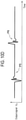
- FIGS. 10A to 10D are time charts showing waveforms in the DC/DC converter of the comparative example.
- FIG. 10A shows a temporal change of a load current IL flowing through the output terminal of the power supply block 30. It can be seen that the load current IL increases in a pulse shape over a certain period of time.
- FIG. 10B shows a temporal change of a driving pulse of the control signal generated by the control block 100.
- the control signal is configured as a driving pulse modulated by PWM and controls on/off of the transistor 31 as the switching element.
- FIG. 10B shows a level at which the transistor 31 is turned on and a level at which the transistor 31 is turned off. Referring to these on/off levels, it can be seen that the transistor 31 is turned on/off at two levels of a saturation region and a cutoff region according to the driving pulse.
- FIG. 10C shows an example of a temporal change of an output voltage Vo of the power supply block 30.
- This example is a case where in the PID model, parameters corresponding to displacement are small and parameters corresponding to integration and differentiation are large.
- a first overshoot P3 is seen at a rising edge of the load current IL
- a second overshoot P4 is seen at a falling edge of the load current IL.
- fluctuation of the voltage is relatively small and the time until the voltage converges to a target value is long.
- FIG. 10D shows another example of the temporal change of the output voltage Vo of the power supply block 30.
- This example is a case where in the PID model, parameters corresponding to displacement are large and parameters corresponding to integration and differentiation are small.
- a first overshoot P5 is seen at a rising edge of the load current IL
- a second overshoot P6 is seen at a falling edge of the load current IL.
- the time until the voltage converges to a target value is relatively short, but fluctuation of the voltage is large.
- the present disclosure can be used for a DC/DC converter or an AC/DC converter.
- a converter capable of quickly converging an output voltage to a target value even in a case of an unexpected fluctuation, and furthermore, capable of reducing overshoot, ringing, noise, and loss that may occur due to the fluctuation.
Landscapes
- Engineering & Computer Science (AREA)
- Physics & Mathematics (AREA)
- Power Engineering (AREA)
- Theoretical Computer Science (AREA)
- General Health & Medical Sciences (AREA)
- General Engineering & Computer Science (AREA)
- Biophysics (AREA)
- Computational Linguistics (AREA)
- Data Mining & Analysis (AREA)
- Evolutionary Computation (AREA)
- Artificial Intelligence (AREA)
- Molecular Biology (AREA)
- Computing Systems (AREA)
- Biomedical Technology (AREA)
- General Physics & Mathematics (AREA)
- Mathematical Physics (AREA)
- Software Systems (AREA)
- Life Sciences & Earth Sciences (AREA)
- Health & Medical Sciences (AREA)
- Dc-Dc Converters (AREA)
- Feedback Control In General (AREA)
Abstract
Description
- This application is based upon and claims the benefit of priority from
Japanese Patent Application No. 2020-135539, filed on August 11, 2020 - The present disclosure relates to a control device for controlling a converter, and a converter.
- DC/DC converters and AC/DC converters that respectively convert input DC and AC power into DC power of a predetermined voltage by using pulse width modulation (PWM), and supply the converted DC power are known in the related art. In such converters, in order to reduce a fluctuation in output voltage that may occur due to a fluctuation in load and to supply DC power in a stable manner, a PID control, in which a feedback-control using a deviation from a target value and integral and derivative of the deviation is performed, has sometimes been used. In the related art, a DC/DC converter that switches between a PID control and a fuzzy control by an artificial intelligence neural network is known.
- On the other hand, a RegimeCast method is also known in the related art. In the RegimeCast method, long-term event prediction is realized by discovering features from among large-scale data streams such as sensor data and automatically recognizing potential time-series patterns, that is, regimes, by extending the concept of "regime shift" in a natural ecosystem model to express time-series event data as an adaptive nonlinear dynamic system.
-
FIG. 1 is a time chart for explaining RegimeCast. In a latest time frame Xc from a past time tm to a current time tc, actual data of possible regimes are indicated by different thin lines. Future data can be predicted by selecting an optimal model for the actual data from a plurality of models indicated by different thick lines and applying the selected model to a time frame XF from the current time tc to a future time ts. For example, events from the time tc to the time ts in the future time frame XF can be predicted based on an event stream of the latest time frame XC. - By the way, although the PID control performs control so as to follow the target value by adjusting the deviation from the target value and the integration and differentiation of the deviation, it is difficult to respond to all controls. Thus, when controlling against an unexpected fluctuation, it takes time for the output voltage to converge to the target value because overshoot, ringing, noise, loss, or the like occurs in the output voltage.
- Some embodiments of the present disclosure provide a control device and a converter capable of quickly converging an output voltage to a target value even in the case of an unexpected fluctuation in the converter, and furthermore, reducing overshoot, ringing, noise, loss, or the like that may occur due to the fluctuation.
- A control device according to the present disclosure controls an output voltage of a converter. The control device includes: a neural network configured to generate a control signal for controlling a power supply block based on a detection signal from an output stage of the power supply block that supplies power to a load of the converter; a model generator configured to generate a model of a nonlinear dynamic system by machine-learning from the detection signal; a model storage configured to store the model generated by the model generator; and a model switch configured to switch to a model, which is selected from models stored in the model storage and is optimal for a latest detection signal, and provide the switched model to the neural network, wherein the neural network generates the control signal based on a future output voltage predicted by using the model provided by the model switch.
- The control device may further include a waveform generator configured to generate a waveform for driving the power supply block based on the control signal supplied from the neural network. The converter may be a DC/DC converter or an AC/DC converter.
- A converter according to the present disclosure includes a power supply block configured to supply power to a load, and a control block configured to control the power supply block. The control block includes: a neural network that generates a control signal for controlling the power supply block based on a detection signal from an output stage of the power supply block; a model generator that generates a model of a nonlinear dynamic system by machine-learning from the detection signal; a model storage that stores the model generated by the model generator; and a model switch that switches to a model which is selected from models stored in the model storage and is optimal for a latest detection signal, and provides the switched model to the neural network, wherein the neural network generates the control signal based on a future output voltage predicted by using the model provided by the model switch.
- The control block may convert the control signal, which is digital data, supplied from the neural network into an analog signal, and supply the analog signal to the power supply block.
- The power supply block may include a transistor and a diode, which are connected in series between a power supply line and a ground line, and the transistor may be driven based on the control signal from the control block to output a current from a connection node between the transistor and the diode. The neural network may control the transistor to operate in an active region.
- The power supply block may include a first transistor and a second transistor, which are connected in series between a power supply line and a ground line, and the first transistor and the second transistor may be driven based on the control signal from the control block to output a current from a connection node between the first transistor and the second transistor. The neural network may control at least one of the first transistor and the second transistor to operate in an active region.
- The control block and the power supply block may be galvanically insulated from each other. The converter may constitute a DC/DC converter or an AC/DC converter.
- The accompanying drawings, which are incorporated in and constitute a part of the specification, illustrate embodiments of the present disclosure.
-
FIG. 1 is a time chart for explaining RegimeCast. -
FIG. 2 is a diagram showing a schematic configuration of a control device according to a first embodiment. -
FIG. 3 is a diagram showing a schematic configuration of a control device according to a second embodiment. -
FIG. 4 is a diagram showing a schematic configuration of a DC/DC converter according to a third embodiment. -
FIG. 5 is a diagram showing a schematic configuration of a control block of the DC/DC converter according to the third embodiment. -
FIGS. 6A to 6C are time charts showing waveforms in the DC/DC converter according to the third embodiment. -
FIG. 7 is a diagram showing a schematic configuration of a DC/DC converter according to a fourth embodiment. -
FIG. 8 is a diagram showing a schematic configuration of a DC/DC converter according to a fifth embodiment. -
FIG. 9 is a diagram showing a schematic configuration of a DC/DC converter of a comparative example. -
FIGS. 10A to 10D are time charts showing waveforms in the DC/DC converter of the comparative example. - Reference will now be made in detail to various embodiments, examples of which are illustrated in the accompanying drawings. In the following detailed description, numerous specific details are set forth in order to provide a thorough understanding of the present disclosure. However, it will be apparent to one of ordinary skill in the art that the present disclosure may be practiced without these specific details. In other instances, well-known methods, procedures, systems, and components have not been described in detail so as not to unnecessarily obscure aspects of the various embodiments.
- Embodiments of a control device and a DC/DC converter will now be described in detail with reference to the drawings.
- It is assumed that a control device according to embodiments realizes RegimeCast known in the related art by artificial intelligence by a neural network and controls a power supply block of a converter to supply an output voltage of a target value. The control device may be included as a control block in the converter, or may form the converter together with the power supply block. In the present disclosure, a DC/DC converter and an AC/DC converter are collectively referred to as a converter.
-
FIG. 2 is a diagram showing a schematic configuration of a control device according to a first embodiment. Acontrol device 10 includes aneural network 11 that generates a control signal for controlling a power supply block in a converter. Theneural network 11 generates the control signal for controlling the power supply block (not shown) by using a model of a nonlinear dynamic system, based on a detection signal provided from the power supply block. - The detection signal is input to the
neural network 11, as time-series data converted into digital data by an A/D converter (not shown). The detection signal may be at least one or more of an output voltage value, an output current value, an input voltage value, an inductor current value, a capacitor current value, and the like of the power supply block. The control signal generated by using the model is output as digital data from theneural network 11. Theneural network 11 may be an appropriate type of neural network such as a spiking neural network, a recurrent neural network, a convolutional neural network, a fuzzy neural network, and the like. - The
control device 10 includes amodel generator 12 that generates a model by machine-learning from the detection signal supplied from the power supply block. Themodel generator 12 learns the detection signal as learning data to generate a model of a nonlinear dynamic system. For example, themodel generator 12 may determine parameters of the model of the nonlinear dynamic system. - The same detection signal input to the
neural network 11 is input to themodel generator 12. The detection signal is time-series data converted into a digital signal by an A/D converter (not shown). - The
control device 10 includes amodel storage 13 that stores the model generated by themodel generator 12. Data of the model generated by themodel generator 12 are supplied to themodel storage 13. The data of the model may be, for example, parameters of the model of the nonlinear dynamic system. Themodel storage 13 may be configured by a nonvolatile memory. - The
control device 10 includes amodel switch 14 that switches the model stored in themodel storage 13 and provides it to theneural network 11. The same detection signal input to theneural network 11 is input to themodel switch 14 through a signal line (not shown). The detection signal is time-series data converted into a digital signal by an A/D converter (not shown). - Based on the time-series data of the input detection signal, the
model switch 14 adaptively switches to an optimal model for the time-series data in real time from among a plurality of models stored in themodel storage 13, and provides the optimal model to theneural network 11. The model may be given by parameters of the model of the nonlinear dynamic system. - The
neural network 11 uses the model provided from themodel switch 14 to generate the control signal for controlling the power supply block based on the time-series data of the detection signal. Theneural network 11 can predict future time-series data by expressing the time-series data as an adaptive nonlinear dynamic system by the concept of regime shift, and can generate the control signal that controls the power supply block so as to perform quick convergence to a target value. As the model selected from themodel switch 14, parameters of the nonlinear dynamic system of the model may be provided to theneural network 11. The neural network outputs the control signal as digital data. - The
control device 10 includes awaveform generator 15 that converts the control signal, which is digital data supplied from theneural network 11, into an analog signal waveform and provides the analog signal waveform to the power supply block. Thewaveform generator 15 may be configured by a D/A converter. Thewaveform generator 15 generates a waveform necessary for controlling on/off of a single transistor serving as a corresponding switching element in the power supply block. Here, the power supply block may include a single transistor as a switching element even when the power supply block constitutes a DC/DC converter or a single-phase AC/DC converter. - As described above, in the
control device 10, themodel generator 12 generates various models from a piece of time-series data based on the detection signal, themodel storage 13 stores the generated models, and themodel switch 14 selects the optimal model in real time from the models stored in themodel storage 13 based on the time-series data of the detection signal. Theneural network 11 uses the model provided from themodel switch 14 to generate a predicted value that predicts a future output voltage of the power supply block based on the time-series data of the detection signal, generates an appropriate control signal based on this predicted value so that the predicted value converges to the target value, and provides the generated control signal to the power supply block through thewaveform generator 15. - Therefore, in the
control device 10, an appropriate control signal can be generated at a timing when control is required, based on the time-series data of the detection signal. Accordingly, the output voltage of thepower supply block 30 can be quickly converged to the target value even in the case of an unexpected fluctuation, and furthermore, overshoot, ringing, noise, loss, and the like that may occur due to the fluctuation can be reduced. - In addition, the
control device 10 may be provided alone to control the power supply block, or may form a DC/DC converter or a single-phase AC/DC converter together with the power supply block. Further, thecontrol device 10 may be configured as a single device by a semiconductor integrated circuit, or theneural network 11, themodel generator 12, themodel storage 13, themodel switch 14, and thewaveform generator 15 may be configured by individual devices. Theneural network 11, themodel generator 12, and themodel switch 14 may be configured as logic blocks in a single device. -
FIG. 3 is a diagram showing a schematic configuration of a control device according to a second embodiment. The control device according to the second embodiment and thecontrol device 10 according to the first embodiment shown inFIG. 2 are common in that they both include: theneural network 11 that generates the control signal for controlling the power supply block in the converter; themodel generator 12 that generates the model by machine-learning from the detection signal supplied from the power supply block; themodel storage 13 that stores the model generated by themodel generator 12; and themodel switch 14 that switches the model stored in themodel storage 13 and provides it to theneural network 11. For the sake of simplicity, elements common to thecontrol device 10 according to the first embodiment are denoted by the same reference numerals as in the first embodiment. - The
control device 10 according to the second embodiment is different from thecontrol device 10 according to the first embodiment in that the latter has thesingle waveform generator 15 while the former has two waveform generators, i.e., first andsecond waveform generators neural network 11 to thefirst waveform generator 16 and thesecond waveform generator 17, respectively. Thefirst waveform generator 16 and thesecond waveform generator 17 may be configured by D/A converters, respectively, like thewaveform generator 15 of thecontrol device 10 according to the first embodiment. - The
first waveform generator 16 and thesecond waveform generator 17 respectively generate waveforms required for individually controlling on/off of two transistors serving as corresponding switching elements in the power supply block based on the control signals from theneural network 11. Here, the power supply block may include two transistors as switching elements even when the power supply block constitutes a DC/DC converter, a single-phase AC/DC converter, or a two-phase AC/DC converter. - As described above, in the
control device 10 according to the second embodiment, as in thecontrol device 10 according to the first embodiment, theneural network 11 can use an optimal model in real time to generate a predicted value that predicts a future output voltage of the power supply block from time-series data of the detection signal, can generate appropriate control signals based on this predicted value so that the predicted value converges to a target value, and can provide the control signals to the power supply block through thefirst waveform generator 16 and thesecond waveform generator 17. - Therefore, the
control device 10 according to the second embodiment can generate the appropriate control signals at a timing when a control is required, based on the time-series data of the control signals, and can individually control the two transistors included in the power supply block through thefirst waveform generator 16 and thesecond waveform generator 17. For this reason, the output voltage of the power supply block can be quickly converged to the target value even in the case of an unexpected fluctuation, and furthermore, overshoot, ringing, noise, and loss that may occur due to the fluctuation can be reduced. - The
control device 10 according to the second embodiment may be provided alone to control the power supply block, or may form a DC/DC converter, a single-phase AC/DC converter, or a two-phase AC/DC converter together with the power supply block. Further, like thecontrol device 10 according to the first embodiment, thecontrol device 10 according to the second embodiment may be configured as a single device by a semiconductor integrated circuit, or theneural network 11, themodel generator 12, themodel storage 13, themodel switch 14, and the first andsecond waveform generators neural network 11, themodel generator 12, and themodel switch 14 may be configured as logic blocks in a single device. - The
control device 10 according to the second embodiment includes thefirst waveform generator 16 and thesecond waveform generator 17 to generate waveforms of the control signals that individually control on/off of the two transistors serving as the corresponding switching elements in the power supply block, but may include three waveform generators when it is necessary to individually control on/off of three transistors serving as corresponding switching elements in the power supply block in a similar manner. Also in this case, the three waveform generators generate waveforms required to individually control on/off of the three transistors serving as the corresponding switching elements in the power supply block based on control signals from theneural network 11. Here, the power supply block may include the three transistors as the switching elements even when the power supply block constitutes a DC/DC converter, a single-phase AC/DC converter, a two-phase AC/DC converter, or a three-phase AC/DC converter. Similarly, thecontrol device 10 according to the second embodiment may have four or more waveform generators. -
FIG. 4 is a diagram showing a schematic configuration of a DC/DC converter according to a third embodiment. The DC/DC converter constitutes an asynchronous rectification type step-down DC/DC converter. - The DC/DC converter includes a
control block 20 and apower supply block 30, which is driven based on a control signal supplied from thecontrol block 20. Thecontrol block 20 has alogic block 21 having functions of model generation, model switching, and a neural network, and anonvolatile memory 23 that stores models. - In addition, the
control block 20 has an A/D converter 24 configured to convert a detection signal as an analog signal provided from thepower supply block 30 into digital data and provide it to thelogic block 21, and a D/A converter 25 configured to convert a control signal as the digital data output from thelogic block 21 into an analog signal and supply it to thepower supply block 30. Further, thecontrol block 20 has a DC/DC converter 26 for system power supply that supplies power to thecontrol block 20. -
FIG. 5 is a diagram showing a schematic configuration of thecontrol block 20 of the DC/DC converter according to the third embodiment. In thecontrol block 20, thelogic block 21 has aneural network 11 that generates a control signal for controlling thepower supply block 30, amodel generator 12 that generates a model by machine-learning from a detection signal supplied from thepower supply block 30, and amodel switch 14 that selects an optimal model based on the detection signal supplied from thepower supply block 30. - Here, elements of the
logic block 21, which is common with thecontrol device 10 according to the first embodiment, are denoted by the corresponding reference numerals. In addition, thenonvolatile memory 23 and the D/A converter 25 correspond to themodel storage 13 and thewaveform generator 15, respectively, of thecontrol device 10 according to the first embodiment. - The
neural network 11 uses a model of a nonlinear dynamic system to generate the control signal for controlling the power supply block based on the detection signal provided from thepower supply block 30. The detection signal is input as time-series data converted into a digital signal by the A/D converter 24. - The detection signal may be at least one or more of an output voltage value, an output current value, an input voltage value, an inductor current value, a capacitor current value, and the like of the
power supply block 30. The control signal generated by using the model is output as digital data from theneural network 11. Theneural network 11 may be an appropriate type of neural network such as a spiking neural network, a recurrent neural network, a convolutional neural network, or a fuzzy neural network. - The
model generator 12 learns the detection signal as learning data and generates a model of a nonlinear dynamic system. For example, themodel generator 12 may determine parameters of the model of the nonlinear dynamic system. The same detection signal input to theneural network 11 is input to themodel generator 12. The detection signal is time-series data converted into a digital signal by the A/D converter 24. Themodel generator 12 supplies data of the generated model to thenonvolatile memory 23. - Based on the time-series data of the input detection signal, the
model switch 14 adaptively switches to an optimal model for the time-series data in real time from among a plurality of models stored in themodel storage 13, and provides the optimal model to theneural network 11. The model may be given by parameters of the model of the nonlinear dynamic system. - The
neural network 11 uses the model provided from themodel switch 14 to generate the control signal for controlling the power supply block based on the time-series data of the detection signal. Theneural network 11 may predict future time-series data by expressing the time-series data as an adaptive nonlinear dynamic system based on the concept of regime shift, and may generate the control signal to control thepower supply block 30 so as to perform quick convergence to a target value. As the model selected from themodel switch 14, parameters of the nonlinear dynamic system of the model may be provided to theneural network 11. Theneural network 11 outputs the control signal as digital data. - The
nonvolatile memory 23 stores the data of the model supplied from thelogic block 21 and provides the stored data of the model to thelogic block 21. Thenonvolatile memory 23 stores the data of the model supplied from themodel generator 12 of thelogic block 21 and provides the stored data of the model to themodel switch 14 of thelogic block 21. The data of the model may be, for example, parameters of the model of the nonlinear dynamic system. - The D/
A converter 25 generates a waveform required for controlling on/off of a single transistor serving as a corresponding switching element in thepower supply block 30. The A/D converter 24 converts the detection signal from thepower supply block 30 from an analog signal to digital data. The DC/DC converter 26 for system power supply supplies power of a predetermined voltage required for driving thecontrol block 20. - The
control block 20 may be configured as a device by a semiconductor integrated circuit by adding thenonvolatile memory 23, the A/D converter 24, the D/A converter 25, and the like to thelogic block 21, or thelogic block 21, thenonvolatile memory 23, the A/D converter 24, the D/A converter 25, and the DC/DC converter 26 for system power supply may be configured by individual devices. - Referring to
FIG. 4 again, in thepower supply block 30, afirst inductor 35, atransistor 31 serving as a switching element, and adiode 33 are provided in series between a power supply line and a ground line. Thetransistor 31 may be a P-channel MOSFET, and thediode 33 may be a Schottky diode. Afirst capacitor 36 is provided between a connection node between thefirst inductor 35 and a source of thetransistor 31 and the ground line. A symbol PG attached to a line in the drawings denotes that the line is the ground line of the power supply block. A low-pass filter is constituted by thefirst inductor 35 and thefirst capacitor 36. This low-pass filter blocks noise and the like from the power supply line. - A connection node between a drain of the
transistor 31 and a cathode of thediode 33 is connected to an output terminal (not shown) via asecond inductor 37, and an output current is supplied from this node toward the output terminal. Asecond capacitor 38 is provided between a connection node between thesecond inductor 37 and the output terminal and the ground line. A low-pass filter is constituted by thesecond inductor 37 and thesecond capacitor 38. - In the
power supply block 30, a control signal from thecontrol block 20 is supplied to a gate of thetransistor 31, which is the switching element, via adriver 32 to control a drain current. The drain current is supplied from the power supply line and flows toward the output terminal to form the output current. A current generated by a flyback voltage of thesecond inductor 37 flows back via thediode 33. - In the
power supply block 30, since thetransistor 31 is driven according to the control signal from thecontrol block 20, the drain current generally becomes a pulsating current. However, the pulsating current is smoothed by the low-pass filter constituted by thesecond inductor 37 and thesecond capacitor 38, and then is sent to the output terminal. Thus, DC power dropped from a voltage of the power supply line is supplied from the output terminal. - In the
power supply block 30, an output voltage obtained from an output line connected to the output terminal is provided as a detection signal to thecontrol block 20. However, the detection signal is not limited to the output voltage, but may be of other types. As indicated by broken lines inFIG. 4 , the detection signal may be a gate voltage of thetransistor 31, a current of thefirst inductor 35, a source current of thetransistor 31, a current of thesecond inductor 37, or an output current. Further, two or more of the output voltage, the gate voltage, and the like may be detected. Here, the source current and the output current may be detected by current sensors from a source line and the output line, respectively. Further, a current of thefirst capacitor 36 or a current of thesecond capacitor 38 may be detected. The same applies to the following embodiments. -
FIGS. 6A to 6C are time charts showing waveforms in the DC/DC converter according to the third embodiment.FIG. 6A shows a temporal change of a load current IL flowing via the output terminal of thepower supply block 30. It can be seen that the load current IL increases in a pulse shape over a certain period of time.FIG. 6B shows a temporal change of a control signal generated by thecontrol block 20. This control signal is generated by theneural network 11 of thecontrol block 20 based on the detection signal from thepower supply block 30. The control signal shifts from a lower first level to a higher second level at a rising timing of the load current IL through transient vibration over a predetermined period of time, and shifts from the higher second level to the lower first level at a falling timing of the load current IL through transient vibration over a predetermined period of time. -
FIG. 6B shows a level at which thetransistor 31 is turned on and a level at which thetransistor 31 is turned off. Referring to these on/off levels, the lower first level and the higher second level are both located in the middle of the on/off levels. Therefore, it can be seen that thetransistor 31 is controlled to operate not only in a saturation region and a cutoff region corresponding to on/off of thetransistor 31, respectively, but also in an active region between the saturation region and the cutoff region. -
FIG. 6C shows a temporal change of an output voltage Vo of thepower supply block 30. A first overshoot PI is seen at the rising timing of the load current IL, and a second overshoot P2 is seen at the falling timing of the load current IL. However, for both the first overshoot P1 and the second overshoot P2, it can be seen that fluctuation of the voltage is small and the time until convergence is short. - In the DC/DC converter according to the third embodiment, the
control block 20 has thelogic block 21, which includes theneural network 11, themodel generator 12, and themodel switch 14, and thenonvolatile memory 23. Themodel generator 12 generates various models from a single piece of time-series data based on the detection signal and stores the generated models in thenonvolatile memory 23. Themodel switch 14 selects an optimal model in real time from the models stored in thenonvolatile memory 23 based on the time-series data of the detection signal. Theneural network 11 uses the model provided from themodel switch 14 to generate a predicted value that predicts a future output voltage of thepower supply block 30 based on the time-series data of the detection signal, generates an appropriate control signal based on the predicted value so that the predicted value converges to a target value, and provides the control signal to thepower supply block 30 via the D/A converter 25. - Therefore, in the DC/DC converter according to the third embodiment, an appropriate control signal can be generated at a timing when control is required, based on the time-series data of the detection signal. For this reason, the output voltage of the
power supply block 30 can be quickly converged to the target value even in the case of an unexpected fluctuation, and furthermore, overshoot, ringing, noise, and loss that may occur due to the fluctuation can be reduced. - Further, in the DC/DC converter according to the third embodiment, the
transistor 31 serving as the switching element is controlled to operate not only in a saturation region and a cutoff region corresponding to on/off of thetransistor 31, respectively, but also in an active region between the saturation region and the cutoff region. Therefore, the drain current of thetransistor 31 is reduced, so that power consumption of thepower supply block 30 can be reduced and further, power conversion efficiency of the DC/DC converter can be improved. -
FIG. 7 is a diagram showing a schematic configuration of a DC/DC converter according to a fourth embodiment. This DC/DC converter constitutes an asynchronous rectification type insulated step-down DC/DC converter. - The DC/DC converter according to the fourth embodiment and the DC/DC converter according to the third embodiment are common in that the DC/DC converter according to the fourth embodiment has the
control block 20 and thepower supply block 30, which have the same configuration as those of the DC/DC converter according to the third embodiment, but is different from the DC/DC converter according to the third embodiment in that galvanic insulation is provided between thecontrol block 20 and thepower supply block 30. - In a line of a detection signal provided from the
power supply block 30 to thecontrol block 20, a firstgalvanic insulation device 51 is provided between the output line of thepower supply block 30 and the A/D converter 24 of thecontrol block 20. Further, in a line of a control signal supplied from thecontrol block 20 to thepower supply block 30, a secondgalvanic insulation device 52 is provided between the D/A converter 25 of thecontrol block 20 and thedriver 32 of thepower supply block 30. The firstgalvanic insulation device 51 and the secondgalvanic insulation device 52 may be configured by galvanic insulating logic ICs. - The
control block 20 has thelogic block 21 having functions of model generation, model switching, and a neural network, and thenonvolatile memory 23 that stores a model. Thelogic block 21 and thenonvolatile memory 23 have a configuration as shown inFIG. 5 , as in the third embodiment, and operate in the same manner as in the third embodiment. Further, thecontrol block 20 has the A/D converter 24 that converts a detection signal, which is an analog signal provided from thepower supply block 30 via the firstgalvanic insulation device 51, into digital data and provides it to thelogic block 21, and the D/A converter 25 that converts a control signal, which is the digital data output from thelogic block 21, into an analog signal and supplies it to thepower supply block 30 via the secondgalvanic insulation device 52. Further, thecontrol block 20 has the DC/DC converter 26 for system power supply that supplies power to thecontrol block 20. - The
control block 20 may be configured as a device by a semiconductor integrated circuit by adding thenonvolatile memory 23, the A/D converter 24, the D/A converter 25, and the like to thelogic block 21, or thelogic block 21, thenonvolatile memory 23, the A/D converter 24, the D/A converter 25, and the DC/DC converter 26 for system power supply may be configured by individual devices. - In the
power supply block 30, thefirst inductor 35, thetransistor 31 serving as the switching element, and thediode 33 are provided in series between the power supply line and the ground line. Thefirst capacitor 36 is provided between the connection node between thefirst inductor 35 and the source of thetransistor 31 and the ground line. A low-pass filter is constituted by thefirst inductor 35 and thefirst capacitor 36. - The connection node between the drain of the
transistor 31 and the cathode of thediode 33 is connected to the output terminal (not shown) via thesecond inductor 37, and the output current is supplied from this node toward the output terminal. Thesecond capacitor 38 is provided between the connection node between thesecond inductor 37 and the output terminal and the ground line. A low-pass filter is constituted by thesecond inductor 37 and thesecond capacitor 38. - In the
power supply block 30, a control signal from thecontrol block 20 is supplied to the gate of thetransistor 31, which is the switching element, via the D/A converter 25, the secondgalvanic insulation device 52, and thedriver 32 to control the drain current. The drain current is supplied from the power supply line and flows toward the output terminal to form the output current. A current generated by a flyback voltage of thesecond inductor 37 flows back via thediode 33. - In the
power supply block 30, since thetransistor 31 is driven according to the control signal from thecontrol block 20, the drain current generally becomes a pulsating current. However, the pulsating current is smoothed by the low-pass filter constituted by thesecond inductor 37 and thesecond capacitor 38, and then is sent to the output terminal. Thus, DC power dropped from a voltage of the power supply line is supplied from the output terminal. The output voltage is acquired from the output line connected to the output terminal and is provided as the detection signal to the A/D converter 24 of thecontrol block 20 via the firstgalvanic insulation device 51. - In the DC/DC converter according to the fourth embodiment, the
control block 20 and thepower supply block 30 are connected via the firstgalvanic insulation device 51 and the secondgalvanic insulation device 52, so that thecontrol block 20 and thepower supply block 30 are galvanically insulated from each other. Due to the galvanic insulation, noise generated in thepower supply block 30 is blocked by the galvanic insulation, which improves noise resistance of thecontrol block 20. Further, even when a failure occurs in thepower supply block 30, thecontrol block 20 can be protected because the failure is blocked by the galvanic insulation. - In the DC/DC converter according to the fourth embodiment, the
control block 20 has the same configuration as shown inFIG. 5 and operates in the same manner as in the third embodiment. That is, thecontrol block 20 has thelogic block 21 including theneural network 11, themodel generator 12, and themodel switch 14, and thenonvolatile memory 23. Themodel generator 12 generates various models from a piece of time-series data based on the detection signal obtained via the firstgalvanic insulation device 51, and stores the generated models in thenonvolatile memory 23. Themodel switch 14 selects an optimal model in real time from the models stored in thenonvolatile memory 23 based on the time-series data. Theneural network 11 uses the model provided from themodel switch 14 to generate a predicted value that predicts a future output voltage of thepower supply block 30 based on the time-series data, generates an appropriate control signal based on this prediction so that the predicted value converges to a target value, and provides the control signal to thepower supply block 30 through the D/A converter 25. - Therefore, in the DC/DC converter according to the fourth embodiment, an appropriate control signal can be generated at a timing when a control is required, based on the time-series data of the detection signal. For this reason, the output voltage of the
power supply block 30 can be quickly converged to the target value even in the case of an unexpected fluctuation, and furthermore, overshoot, ringing, noise, and loss that may occur due to the fluctuation can be reduced. - Further, in the DC/DC converter according to the fourth embodiment, the
transistor 31 serving as the switching element is controlled to operate not only in a saturation region and a cutoff region corresponding to the on/off of thetransistor 31, respectively, but also in an active region between the saturation region and the cutoff region. Therefore, the drain current of thetransistor 31 is reduced, so that power consumption of thepower supply block 30 can be reduced and further, power conversion efficiency of the DC/DC converter can be improved. -
FIG. 8 is a diagram showing a schematic configuration of a DC/DC converter according to a fifth embodiment. This DC/DC converter constitutes a synchronous rectification type insulated step-down DC/DC converter. - The DC/DC converter according to the fifth embodiment has substantially the same configuration as the DC/DC converter according to the third embodiment except that the
control block 20 and thepower supply block 30 are galvanically insulated from each other, asecond transistor 39 is provided instead of the diode in thepower supply block 30, and thefirst transistor 34 and thesecond transistor 39 form a high-side switching element and a low-side switching element, respectively. For the sake of simplicity, elements common to the DC/DC converter according to the third embodiment are denoted by the same reference numerals as in the third embodiment. - Two control signals, which are two sets of digital data, for controlling the
first transistor 34 as a first switching element and thesecond transistor 39 as a second switching element in thepower supply block 30, respectively, are generated from thelogic block 21 of thecontrol block 20, and are supplied to gates of thefirst transistor 34 and thesecond transistor 39, respectively, via a first D/A converter 27 and a second D/A converter 28, a secondgalvanic insulation device 52 and a thirdgalvanic insulation device 53, and afirst driver 41 and asecond driver 42. - In a line of a detection signal provided from the
power supply block 30 to thecontrol block 20, a firstgalvanic insulation device 51 is provided between the output line of thepower supply block 30 and the A/D converter 24 of thecontrol block 20. Further, as described above, in lines of the two control signals supplied from thecontrol block 20 to thepower supply block 30, the secondgalvanic insulation device 52 and the thirdgalvanic insulation device 53 are provided between the first D/A converter 27 of thecontrol block 20 and thefirst driver 41 of thepower supply block 30 and between the second D/A converter 28 of thecontrol block 20 and thesecond driver 42 of thepower supply block 30, respectively. The firstgalvanic insulation device 51, the secondgalvanic insulation device 52, and the thirdgalvanic insulation device 53 may be configured by a galvanic insulation logic IC. - The
control block 20 has thelogic block 21 having functions of model generation, model switching, and a neural network, and thenonvolatile memory 23 provided to thelogic block 21 for storing a model. Thelogic block 21 and thenonvolatile memory 23 have the same configuration as that shown inFIG. 5 , except that theneural network 11 generates the two control signals, which are the two sets of digital data, for controlling thefirst transistor 34 as the first switching element and thesecond transistor 39 as the second switching element in thepower supply block 30, respectively, and in order to convert these two sets of digital data into analog signals, the D/A converter 25 is replaced with the first D/A converter 27 and the second D/A converter 28. Other configurations are the same as in the third embodiment and operate in the same manner as in the third embodiment. - The
control block 20 further has the A/D converter 24 that converts a detection signal, which is an analog signal provided from thepower supply block 30 via the firstgalvanic insulation device 51, into digital data and provides it to thelogic block 21, and the DC/DC converter 26 for system power supply that supplies power to thecontrol block 20. - The
control block 20 may be configured as a device by a semiconductor integrated circuit by adding thenonvolatile memory 23, the A/D converter 24, the first D/A converter 27, the second D/A converter 28, and the like to thelogic block 21, or thelogic block 21, thenonvolatile memory 23, the A/D converter 24, the first D/A converter 27, the second D/A converter 28, and the DC/DC converter 26 for system power supply may be configured by individual devices. - In the
power supply block 30, thefirst inductor 35, thefirst transistor 34 as the high-side switching element, and asecond transistor 39 as the low-side switching element are provided in series between the power supply line and the ground line. Thefirst transistor 34 and thesecond transistor 39 may be P-channel MOSFETs. Thefirst capacitor 36 is provided between a connection node between thefirst inductor 35 and a source of thefirst transistor 34 and the ground line. A low-pass filter is constituted by thefirst inductor 35 and thefirst capacitor 36. - A connection node between a drain of the
first transistor 34 and a drain of thesecond transistor 39 is connected to an output terminal (not shown) via thesecond inductor 37, and an output current is supplied from this node toward the output terminal. Thesecond capacitor 38 is provided between a connection node between thesecond inductor 37 and the output terminal and the ground line. A low-pass filter is constituted by thesecond inductor 37 and thesecond capacitor 38. - In the
power supply block 30, control signals from thecontrol block 20 are supplied to the gates of thefirst transistor 34 as the first switching element and thesecond transistor 39 as the second switching element, respectively, via the first D/A converter 27, the secondgalvanic insulation device 52 and thefirst driver 41, the second D/A converter 28, and the thirdgalvanic insulation device 53 and thesecond driver 42 to control drain currents. The drain current of thefirst transistor 34 is supplied from the power supply line and flows toward the output terminal. Thesecond transistor 39 flows back a current, which is generated by a flyback voltage of thesecond inductor 37, as the drain current thereof. - In the
power supply block 30, since thefirst transistor 34 and thesecond transistor 39 are driven according to the control signals from thecontrol block 20, the sum of the drain currents of thefirst transistor 34 and thesecond transistor 39 generally becomes a pulsating current. However, the pulsating current is smoothed by the low-pass filter constituted by thesecond inductor 37 and thesecond capacitor 38, and then is sent to the output terminal. Thus, DC power dropped from a voltage of the power supply line is supplied from the output terminal. The output voltage is acquired from the output line connected to the output terminal and is provided as the detection signal to the A/D converter 24 of thecontrol block 20 via the firstgalvanic insulation device 51. - In the DC/DC converter according to the fifth embodiment, the
control block 20 and thepower supply block 30 are connected via the firstgalvanic insulation device 51, the secondgalvanic insulation device 52, and the thirdgalvanic insulation device 53, so that they are galvanically insulated from each other. Due to the galvanic insulation, noise generated in thepower supply block 30 is blocked by the galvanic insulation, so that noise resistance of thecontrol block 20 is improved. Further, even when a failure occurs in thepower supply block 30, the failure is blocked by the galvanic insulation, so that thecontrol block 20 can be protected. - The DC/DC converter according to the fifth embodiment adopts a structure of a synchronous rectification type in which the
second transistor 39 is adopted instead of thediode 33 in the DC/DC converter according to the third embodiment and the DC/DC converter according to the fourth embodiment, and in which thefirst transistor 34 of a high-side and thesecond transistor 39 of a low-side are provided in series between the power supply line and the ground line. Thesecond transistor 39 can suppress a voltage drop in an on state to be smaller than that in the case of using thediode 33. Thus, power consumption of thepower supply block 30 can be reduced, and furthermore, power conversion efficiency of the DC/DC converter can be improved. - In the DC/DC converter according to the fifth embodiment, the
control block 20 has the same configuration as shown inFIG. 5 and operates in the same manner as in the third embodiment. That is, thecontrol block 20 has thelogic block 21 including theneural network 11, themodel generator 12, and themodel switch 14, and thenonvolatile memory 23. Themodel generator 12 generates various models from a piece of time-series data, which is the detection signal obtained via the firstgalvanic insulation device 51, and stores the generated models in thenonvolatile memory 23. Themodel switch 14 selects an optimal model in real time from the models stored in thenonvolatile memory 23 based on the time-series data. Theneural network 11 uses the model provided from themodel switch 14 to generate a predicted value that predicts a future output voltage of thepower supply block 30 based on the time-series data, generates appropriate control signals based on this prediction so that the predicted value converges to a target value, and provides the control signals to thepower supply block 30 via the first D/A converter 27 and the second D/A converter 28. - Therefore, in the DC/DC converter according to the fifth embodiment, the appropriate control signals can be generated at a timing when control is required, based on the time-series data of the detection signal. Therefore, the output voltage of the
power supply block 30 can be quickly converged to the target value even in the case of an unexpected fluctuation, and furthermore, overshoot, ringing, noise, and loss that may occur due to the fluctuation can be reduced. - Further, in the DC/DC converter according to the fifth embodiment, the
first transistor 34 and thesecond transistor 39 serving as the first switching element and the second switching element, respectively, are controlled to operate not only in saturation regions and cutoff regions corresponding to on/off of the first andsecond transistors first transistor 34 and thesecond transistor 39 are reduced, so that power consumption of thepower supply block 30 can be reduced and further, power conversion efficiency of the DC/DC converter can be improved. -
FIG. 9 is a diagram showing a schematic configuration of a DC/DC converter of a comparative example. This DC/DC converter constitutes an asynchronous rectification type step-down DC/DC converter using a PID control. - The DC/DC converter has a
control block 100 and apower supply block 30 driven based on a control signal supplied from thecontrol block 100. Since thepower supply block 30 has the same configuration as thepower supply block 30 of the DC/DC converter according to the third embodiment, common elements are denoted by the same reference numerals for the sake of simplicity. - The
control block 100 has alogic block 101. Thelogic block 101 has a PID model part that generates a control signal for controlling thepower supply block 30 according to a PID model, and a pulse generator that generates a driving pulse by pulse width modulation (PWM) for driving thepower supply block 30 based on the control signal generated by the PID model part. The PID model part performs a feedback control by using coefficients of a deviation from a target value and integration and differentiation of the deviation as parameters. The PID model part uses a PID model of an output voltage of thepower supply block 30 to generate the control signal so that the output voltage of thepower supply block 30 follows the target value. The pulse generator PWM-modulates the control signal generated by the PID model part to generate a driving pulse for driving thepower supply block 30. - The
control block 100 has aconfiguration ROM 102 that stores parameters and the like to be used in the PID model part, and a DC/DC converter 103 for system power supply for supplying power to thecontrol block 100. Theconfiguration ROM 102 can provide the stored parameters of the PID model to the PID model part of thelogic block 101. The parameters of the PID model stored in theconfiguration ROM 102 may be updated as needed. - In the
power supply block 30, afirst inductor 35, atransistor 31 as a switching element, and adiode 33 are provided in series between a power supply line and a ground line. Thetransistor 31 may be a P-channel MOSFET and thediode 33 may be a Schottky diode. Afirst capacitor 36 is provided between a connection node between thefirst inductor 35 and a source of thetransistor 31 and the ground line. A low-pass filter is constituted by thefirst inductor 35 and thefirst capacitor 36. This low-pass filter blocks noise and the like from the power supply line. - A connection node between a drain of the
transistor 31 and a cathode of thediode 33 is connected to an output terminal (not shown) via asecond inductor 37, and an output current is supplied from this node toward the output terminal. Asecond capacitor 38 is provided between a connection node between thesecond inductor 37 and the output terminal and the ground line. A low-pass filter is constituted by thesecond inductor 37 and thesecond capacitor 38. - In the
power supply block 30, the driving pulse from thecontrol block 100 is supplied to a gate of thetransistor 31, which is the switching element, via thedriver 32 to control a drain current. The drain current is supplied from the power supply line and flows toward the output terminal to form an output current. A current generated by a flyback voltage of thesecond inductor 37 flows back through thediode 33. - In the
power supply block 30, since thetransistor 31 is driven according to the driving pulse from thecontrol block 100, the drain current generally becomes a pulsating current. However, the pulsating current is smoothed by the low-pass filter constituted by thesecond inductor 37 and thesecond capacitor 38 and then is sent to the output terminal. Thus, DC power dropped from a voltage of the power supply line is supplied from the output terminal. The output voltage is acquired from an output line connected to the output terminal and is provided as a detection signal to thecontrol block 100. -
FIGS. 10A to 10D are time charts showing waveforms in the DC/DC converter of the comparative example.FIG. 10A shows a temporal change of a load current IL flowing through the output terminal of thepower supply block 30. It can be seen that the load current IL increases in a pulse shape over a certain period of time.FIG. 10B shows a temporal change of a driving pulse of the control signal generated by thecontrol block 100. The control signal is configured as a driving pulse modulated by PWM and controls on/off of thetransistor 31 as the switching element. -
FIG. 10B shows a level at which thetransistor 31 is turned on and a level at which thetransistor 31 is turned off. Referring to these on/off levels, it can be seen that thetransistor 31 is turned on/off at two levels of a saturation region and a cutoff region according to the driving pulse. -
FIG. 10C shows an example of a temporal change of an output voltage Vo of thepower supply block 30. This example is a case where in the PID model, parameters corresponding to displacement are small and parameters corresponding to integration and differentiation are large. A first overshoot P3 is seen at a rising edge of the load current IL, and a second overshoot P4 is seen at a falling edge of the load current IL. However, for both the first overshoot P3 and the second overshoot P4, it can be seen that fluctuation of the voltage is relatively small and the time until the voltage converges to a target value is long. -
FIG. 10D shows another example of the temporal change of the output voltage Vo of thepower supply block 30. This example is a case where in the PID model, parameters corresponding to displacement are large and parameters corresponding to integration and differentiation are small. A first overshoot P5 is seen at a rising edge of the load current IL, and a second overshoot P6 is seen at a falling edge of the load current IL. However, for both the first overshoot P5 and the second overshoot P6, it can be seen that the time until the voltage converges to a target value is relatively short, but fluctuation of the voltage is large. - The present disclosure can be used for a DC/DC converter or an AC/DC converter.
- According to the present disclosure in some embodiments, it is possible to provide a converter capable of quickly converging an output voltage to a target value even in a case of an unexpected fluctuation, and furthermore, capable of reducing overshoot, ringing, noise, and loss that may occur due to the fluctuation.
- While certain embodiments have been described, these embodiments have been presented by way of example only, and are not intended to limit the scope of the disclosures. Indeed, the embodiments described herein may be embodied in a variety of other forms. Furthermore, various omissions, substitutions and changes in the form of the embodiments described herein may be made. The accompanying claims and their equivalents are intended to cover such forms or modifications as would fall within the scope of the disclosures.
Claims (11)
- A control device (10) that controls an output voltage of a converter, comprising:a neural network (11) configured to generate a control signal for controlling a power supply block (30) based on a detection signal from an output stage of the power supply block (30) that supplies power to a load of the converter;a model generator (12) configured to generate a model of a nonlinear dynamic system by machine-learning from the detection signal;a model storage (13) configured to store the model generated by the model generator (12); anda model switch (14) configured to switch to a model, which is selected from models stored in the model storage (13) and is optimal for a latest detection signal, and provide the switched model to the neural network (11),wherein the neural network (11) generates the control signal based on a future output voltage predicted by using the model provided by the model switch (14).
- The control device (10) of Claim 1, further comprising a waveform generator (15, 16, 17) configured to generate a waveform for driving the power supply block (30) based on the control signal supplied from the neural network (11).
- The control device (10) of Claim 1 or 2, wherein the converter is a DC/DC converter or an AC/DC converter.
- A converter comprising:a power supply block (30) configured to supply power to a load; anda control block (20) configured to control the power supply block (30),wherein the control block (20) includes:a neural network (11) that generates a control signal for controlling the power supply block (30) based on a detection signal from an output stage of the power supply block (30);a model generator (12) that generates a model of a nonlinear dynamic system by machine-learning from the detection signal;a model storage (13) that stores the model generated by the model generator (12); anda model switch (14) that switches to a model which is selected from models stored in the model storage (13) and is optimal for a latest detection signal, and provides the switched model to the neural network (11), andwherein the neural network (11) generates the control signal based on a future output voltage predicted by using the model provided by the model switch (14).
- The converter of Claim 4, wherein the control block (20) further includes a D/A converter (25, 27, 28) that converts the control signal, which is digital data, supplied from the neural network (11) into an analog signal, and supplies the analog signal to the power supply block (30).
- The converter of Claim 4 or 5, wherein the power supply block (30) includes a transistor (31) and a diode (33), which are connected in series between a power supply line and a ground line, and the transistor (31) is driven based on the control signal from the control block (20) to output a current from a connection node between the transistor (31) and the diode (33).
- The converter of Claim 6, wherein the neural network (11) controls the transistor (31) to operate in an active region.
- The converter of Claim 4 or 5, wherein the power supply block (30) includes a first transistor (34) and a second transistor (39), which are connected in series between a power supply line and a ground line, and the first transistor (34) and the second transistor (39) are driven based on the control signal from the control block (20) to output a current from a connection node between the first transistor (34) and the second transistor (39).
- The converter of Claim 8, wherein the neural network (11) controls at least one of the first transistor (34) and the second transistor (39) to operate in an active region.
- The converter of any one of Claims 4 to 9, wherein the control block (20) and the power supply block (30) are galvanically insulated from each other.
- The converter of any one of Claims 4 to 10, wherein the converter constitutes a DC/DC converter or an AC/DC converter.
Applications Claiming Priority (1)
| Application Number | Priority Date | Filing Date | Title |
|---|---|---|---|
| JP2020135539A JP7499110B2 (en) | 2020-08-11 | 2020-08-11 | Control device and converter |
Publications (1)
| Publication Number | Publication Date |
|---|---|
| EP3955449A1 true EP3955449A1 (en) | 2022-02-16 |
Family
ID=77226617
Family Applications (1)
| Application Number | Title | Priority Date | Filing Date |
|---|---|---|---|
| EP21189719.4A Withdrawn EP3955449A1 (en) | 2020-08-11 | 2021-08-04 | Control device and converter |
Country Status (3)
| Country | Link |
|---|---|
| US (1) | US20220051097A1 (en) |
| EP (1) | EP3955449A1 (en) |
| JP (1) | JP7499110B2 (en) |
Families Citing this family (1)
| Publication number | Priority date | Publication date | Assignee | Title |
|---|---|---|---|---|
| US20230117488A1 (en) * | 2021-10-18 | 2023-04-20 | Infineon Technologies Austria Ag | Interpretable Neural Networks for Nonlinear Control |
Citations (1)
| Publication number | Priority date | Publication date | Assignee | Title |
|---|---|---|---|---|
| WO2020148808A1 (en) * | 2019-01-15 | 2020-07-23 | 三菱電機株式会社 | Control device for power converter |
Family Cites Families (12)
| Publication number | Priority date | Publication date | Assignee | Title |
|---|---|---|---|---|
| JPS5320104B2 (en) * | 1972-07-09 | 1978-06-24 | ||
| JPH04211802A (en) * | 1990-07-25 | 1992-08-03 | Toshiba Corp | Neural network device |
| JPH05244770A (en) * | 1992-02-27 | 1993-09-21 | Koufu Nippon Denki Kk | Dc-dc converter |
| US7675279B2 (en) | 2004-12-21 | 2010-03-09 | Rohm Co., Ltd. | Switching regulator soft start circuitry using a D/A converter |
| EP3125065B1 (en) * | 2015-07-31 | 2018-12-19 | Power Integrations Switzerland GmbH | Communicating across galvanic isolation |
| US11347296B2 (en) * | 2017-07-25 | 2022-05-31 | Dell Products, L.P. | Backlight dimming via buck-boost conversion in an information handling system |
| CN111670609B (en) | 2018-01-29 | 2022-11-04 | 罗姆股份有限公司 | Light-emitting element drive control device, light-emitting element drive circuit device |
| EP3754827A4 (en) | 2018-02-16 | 2021-03-17 | Mitsubishi Electric Corporation | POWER CONVERTER CONTROL DEVICE |
| JP7189075B2 (en) | 2018-05-14 | 2022-12-13 | 株式会社神戸製鋼所 | MOTOR DRIVE CONTROL APPARATUS AND METHOD, AND MOTOR DRIVE CONTROL SYSTEM |
| JP7148380B2 (en) | 2018-12-10 | 2022-10-05 | ローム株式会社 | Drive modules, power controllers, switching power supplies |
| US11837958B2 (en) * | 2018-12-12 | 2023-12-05 | Infineon Technologies Austria Ag | Multiphase power converter |
| US10996728B2 (en) * | 2019-01-04 | 2021-05-04 | Sigmasense, Llc. | Power supply signal conditioning system based on drive-sense circuit (DSC) processing |
-
2020
- 2020-08-11 JP JP2020135539A patent/JP7499110B2/en active Active
-
2021
- 2021-08-04 EP EP21189719.4A patent/EP3955449A1/en not_active Withdrawn
- 2021-08-09 US US17/397,120 patent/US20220051097A1/en not_active Abandoned
Patent Citations (1)
| Publication number | Priority date | Publication date | Assignee | Title |
|---|---|---|---|---|
| WO2020148808A1 (en) * | 2019-01-15 | 2020-07-23 | 三菱電機株式会社 | Control device for power converter |
Non-Patent Citations (2)
| Title |
|---|
| DRAGICEVIC TOMISLAV ET AL: "Weighting Factor Design in Model Predictive Control of Power Electronic Converters: An Artificial Neural Network Approach", IEEE TRANSACTIONS ON INDUSTRIAL ELECTRONICS, IEEE SERVICE CENTER, PISCATAWAY, NJ, USA, vol. 66, no. 11, 1 November 2019 (2019-11-01), pages 8870 - 8880, XP011733218, ISSN: 0278-0046, [retrieved on 20190701], DOI: 10.1109/TIE.2018.2875660 * |
| HIDENORI MARUTA ET AL: "Reference modification control DC-DC converter with neural network predictor", CONTROL AND MODELING FOR POWER ELECTRONICS (COMPEL), 2012 IEEE 13TH WORKSHOP ON, IEEE, 10 June 2012 (2012-06-10), pages 1 - 4, XP032211937, ISBN: 978-1-4244-9372-2, DOI: 10.1109/COMPEL.2012.6251806 * |
Also Published As
| Publication number | Publication date |
|---|---|
| JP2022032080A (en) | 2022-02-25 |
| JP7499110B2 (en) | 2024-06-13 |
| US20220051097A1 (en) | 2022-02-17 |
Similar Documents
| Publication | Publication Date | Title |
|---|---|---|
| US6037755A (en) | Switching controller for a buck+boost converter and method of operation thereof | |
| US6400127B1 (en) | Dual mode pulse-width modulator for power control applications | |
| CN101640481B (en) | Mixed power converter | |
| US9093901B2 (en) | Switching converter and method for controlling a switching converter | |
| Chen et al. | A low-power dual-frequency SIMO buck converter topology with fully-integrated outputs and fast dynamic operation in 45 nm CMOS | |
| US8274264B2 (en) | Digital control method for improving heavy-to-light (step down) load transient response of switch mode power supplies | |
| US20100097045A1 (en) | Single inductor multiple output power supply | |
| JP3887368B2 (en) | Low loss DC / DC converter | |
| US9203316B2 (en) | DC-DC converter | |
| KR20100130161A (en) | Multiphase Boost Converter and How It Works | |
| US11522459B2 (en) | Combining temperature monitoring and true different current sensing in a multiphase voltage regulator | |
| US20060007617A1 (en) | DC voltage converter and method for converting a DC voltage | |
| EP3232553B1 (en) | Dc-dc converter | |
| US20190190373A1 (en) | Multi Output Three Level Buck Converter | |
| US10056837B2 (en) | DC-DC converter and power source device | |
| JP2017147787A (en) | Multi-output dc-dc converter | |
| KR20160110241A (en) | Method for operating a power converter circuit and power converter circuit | |
| US20080238382A1 (en) | Anti-ringing switching regulator and control method therefor | |
| KR20220128264A (en) | Control method, apparatus, system and electronic device of synchronous BUCK circuit | |
| US7253592B2 (en) | DC voltage converter and method for converting a DC voltage | |
| US12609619B2 (en) | Multi-mode buck-boost converter and control method with shared capacitor | |
| EP3955449A1 (en) | Control device and converter | |
| US7583066B2 (en) | Method of operating a DC/DC up/down converter | |
| NL2029902B1 (en) | A series resonant converter for balancing a bipolar Direct Current, DC, power grid, as well as a corresponding arrangement, method and computer program product. | |
| JP5418817B2 (en) | DC-DC converter |
Legal Events
| Date | Code | Title | Description |
|---|---|---|---|
| PUAI | Public reference made under article 153(3) epc to a published international application that has entered the european phase |
Free format text: ORIGINAL CODE: 0009012 |
|
| STAA | Information on the status of an ep patent application or granted ep patent |
Free format text: STATUS: THE APPLICATION HAS BEEN PUBLISHED |
|
| AK | Designated contracting states |
Kind code of ref document: A1 Designated state(s): AL AT BE BG CH CY CZ DE DK EE ES FI FR GB GR HR HU IE IS IT LI LT LU LV MC MK MT NL NO PL PT RO RS SE SI SK SM TR |
|
| STAA | Information on the status of an ep patent application or granted ep patent |
Free format text: STATUS: REQUEST FOR EXAMINATION WAS MADE |
|
| 17P | Request for examination filed |
Effective date: 20220706 |
|
| RBV | Designated contracting states (corrected) |
Designated state(s): AL AT BE BG CH CY CZ DE DK EE ES FI FR GB GR HR HU IE IS IT LI LT LU LV MC MK MT NL NO PL PT RO RS SE SI SK SM TR |
|
| STAA | Information on the status of an ep patent application or granted ep patent |
Free format text: STATUS: EXAMINATION IS IN PROGRESS |
|
| 17Q | First examination report despatched |
Effective date: 20221222 |
|
| STAA | Information on the status of an ep patent application or granted ep patent |
Free format text: STATUS: THE APPLICATION IS DEEMED TO BE WITHDRAWN |
|
| 18D | Application deemed to be withdrawn |
Effective date: 20250121 |