EP3955318A1 - Feed-through wiring solution for solar cell modules - Google Patents
Feed-through wiring solution for solar cell modules Download PDFInfo
- Publication number
- EP3955318A1 EP3955318A1 EP21181717.6A EP21181717A EP3955318A1 EP 3955318 A1 EP3955318 A1 EP 3955318A1 EP 21181717 A EP21181717 A EP 21181717A EP 3955318 A1 EP3955318 A1 EP 3955318A1
- Authority
- EP
- European Patent Office
- Prior art keywords
- solar cell
- contact pad
- laminate substrate
- cell module
- top surface
- Prior art date
- Legal status (The legal status is an assumption and is not a legal conclusion. Google has not performed a legal analysis and makes no representation as to the accuracy of the status listed.)
- Granted
Links
Images




Classifications
-
- H—ELECTRICITY
- H10—SEMICONDUCTOR DEVICES; ELECTRIC SOLID-STATE DEVICES NOT OTHERWISE PROVIDED FOR
- H10F—INORGANIC SEMICONDUCTOR DEVICES SENSITIVE TO INFRARED RADIATION, LIGHT, ELECTROMAGNETIC RADIATION OF SHORTER WAVELENGTH OR CORPUSCULAR RADIATION
- H10F77/00—Constructional details of devices covered by this subclass
- H10F77/93—Interconnections
- H10F77/933—Interconnections for devices having potential barriers
- H10F77/935—Interconnections for devices having potential barriers for photovoltaic devices or modules
-
- H—ELECTRICITY
- H10—SEMICONDUCTOR DEVICES; ELECTRIC SOLID-STATE DEVICES NOT OTHERWISE PROVIDED FOR
- H10F—INORGANIC SEMICONDUCTOR DEVICES SENSITIVE TO INFRARED RADIATION, LIGHT, ELECTROMAGNETIC RADIATION OF SHORTER WAVELENGTH OR CORPUSCULAR RADIATION
- H10F19/00—Integrated devices, or assemblies of multiple devices, comprising at least one photovoltaic cell covered by group H10F10/00, e.g. photovoltaic modules
-
- H—ELECTRICITY
- H10—SEMICONDUCTOR DEVICES; ELECTRIC SOLID-STATE DEVICES NOT OTHERWISE PROVIDED FOR
- H10F—INORGANIC SEMICONDUCTOR DEVICES SENSITIVE TO INFRARED RADIATION, LIGHT, ELECTROMAGNETIC RADIATION OF SHORTER WAVELENGTH OR CORPUSCULAR RADIATION
- H10F19/00—Integrated devices, or assemblies of multiple devices, comprising at least one photovoltaic cell covered by group H10F10/00, e.g. photovoltaic modules
- H10F19/80—Encapsulations or containers for integrated devices, or assemblies of multiple devices, having photovoltaic cells
- H10F19/807—Double-glass encapsulation, e.g. photovoltaic cells arranged between front and rear glass sheets
-
- H—ELECTRICITY
- H10—SEMICONDUCTOR DEVICES; ELECTRIC SOLID-STATE DEVICES NOT OTHERWISE PROVIDED FOR
- H10F—INORGANIC SEMICONDUCTOR DEVICES SENSITIVE TO INFRARED RADIATION, LIGHT, ELECTROMAGNETIC RADIATION OF SHORTER WAVELENGTH OR CORPUSCULAR RADIATION
- H10F19/00—Integrated devices, or assemblies of multiple devices, comprising at least one photovoltaic cell covered by group H10F10/00, e.g. photovoltaic modules
- H10F19/80—Encapsulations or containers for integrated devices, or assemblies of multiple devices, having photovoltaic cells
- H10F19/85—Protective back sheets
-
- H—ELECTRICITY
- H10—SEMICONDUCTOR DEVICES; ELECTRIC SOLID-STATE DEVICES NOT OTHERWISE PROVIDED FOR
- H10F—INORGANIC SEMICONDUCTOR DEVICES SENSITIVE TO INFRARED RADIATION, LIGHT, ELECTROMAGNETIC RADIATION OF SHORTER WAVELENGTH OR CORPUSCULAR RADIATION
- H10F19/00—Integrated devices, or assemblies of multiple devices, comprising at least one photovoltaic cell covered by group H10F10/00, e.g. photovoltaic modules
- H10F19/90—Structures for connecting between photovoltaic cells, e.g. interconnections or insulating spacers
- H10F19/902—Structures for connecting between photovoltaic cells, e.g. interconnections or insulating spacers for series or parallel connection of photovoltaic cells
-
- H—ELECTRICITY
- H10—SEMICONDUCTOR DEVICES; ELECTRIC SOLID-STATE DEVICES NOT OTHERWISE PROVIDED FOR
- H10F—INORGANIC SEMICONDUCTOR DEVICES SENSITIVE TO INFRARED RADIATION, LIGHT, ELECTROMAGNETIC RADIATION OF SHORTER WAVELENGTH OR CORPUSCULAR RADIATION
- H10F19/00—Integrated devices, or assemblies of multiple devices, comprising at least one photovoltaic cell covered by group H10F10/00, e.g. photovoltaic modules
- H10F19/90—Structures for connecting between photovoltaic cells, e.g. interconnections or insulating spacers
- H10F19/902—Structures for connecting between photovoltaic cells, e.g. interconnections or insulating spacers for series or parallel connection of photovoltaic cells
- H10F19/904—Structures for connecting between photovoltaic cells, e.g. interconnections or insulating spacers for series or parallel connection of photovoltaic cells characterised by the shapes of the structures
-
- H—ELECTRICITY
- H10—SEMICONDUCTOR DEVICES; ELECTRIC SOLID-STATE DEVICES NOT OTHERWISE PROVIDED FOR
- H10F—INORGANIC SEMICONDUCTOR DEVICES SENSITIVE TO INFRARED RADIATION, LIGHT, ELECTROMAGNETIC RADIATION OF SHORTER WAVELENGTH OR CORPUSCULAR RADIATION
- H10F19/00—Integrated devices, or assemblies of multiple devices, comprising at least one photovoltaic cell covered by group H10F10/00, e.g. photovoltaic modules
- H10F19/90—Structures for connecting between photovoltaic cells, e.g. interconnections or insulating spacers
-
- Y—GENERAL TAGGING OF NEW TECHNOLOGICAL DEVELOPMENTS; GENERAL TAGGING OF CROSS-SECTIONAL TECHNOLOGIES SPANNING OVER SEVERAL SECTIONS OF THE IPC; TECHNICAL SUBJECTS COVERED BY FORMER USPC CROSS-REFERENCE ART COLLECTIONS [XRACs] AND DIGESTS
- Y02—TECHNOLOGIES OR APPLICATIONS FOR MITIGATION OR ADAPTATION AGAINST CLIMATE CHANGE
- Y02E—REDUCTION OF GREENHOUSE GAS [GHG] EMISSIONS, RELATED TO ENERGY GENERATION, TRANSMISSION OR DISTRIBUTION
- Y02E10/00—Energy generation through renewable energy sources
- Y02E10/50—Photovoltaic [PV] energy
Definitions
- the present disclosure is related generally to solar cell modules and more specifically to a feed-through wiring solution for a solar cell array comprising a plurality of solar cell modules.
- a solar array generally is comprised of multiple solar cell modules connected together to produce electric power. Wiring must be completed across the solar cell modules to carry power to other devices.
- Current methods for extracting current from individual solar cell modules and routing them to the power bus for the solar cell array involves either flexible tabs that extend from the edge of each solar cell module or wires that are welded or soldered to the traces at the front side of each solar cell module. Getting the power from the front to the back side of the solar cell modules thus typically involves either allocating a sufficient gap between solar cell modules to enable wrapping of the wires or the flexible tabs around to the back of the assembly or including feed-through holes in the assembly to pass the wires from the front to the back of the solar cell modules.
- the present disclosure provides a solar cell module.
- the solar cell module includes (a) a laminate substrate having a first surface and a second surface opposite the first surface, (b) a solar cell positioned on the first surface of the laminate substrate, (c) a first contact pad positioned on the first surface of the laminate substrate adjacent to the solar cell, (d) a second contact pad positioned on the second surface of the laminate substrate, (e) one or more vias positioned through the laminate substrate to electrically connect the first contact pad to the second contact pad, and (f) one or more interconnects extending from the solar cell and electrically coupling the solar cell to the first contact pad.
- the present disclosure provides a solar cell array.
- the solar cell array comprises (a) a plurality of solar cell modules, wherein each of the plurality of solar cell modules includes (i) a laminate substrate having a first surface and a second surface opposite the first surface, (ii) a solar cell positioned on the first surface of the laminate substrate, (iii) a first contact pad positioned on the first surface of the laminate substrate adjacent to the solar cell, (iv) a second contact pad positioned on the second surface of the laminate substrate, (v) one or more vias positioned through the laminate substrate to electrically connect the first contact pad to the second contact pad, (vi) one or more interconnects extending from the solar cell and electrically coupling the solar cell to the first contact pad, and (b) a panel coupled to the laminate substrate of each of the plurality of solar cell modules, wherein adjacent solar cell modules of the plurality of solar cell modules abut one another such that there is not a gap therebetween.
- a method for fabricating a solar cell module includes (a) positioning a solar cell on a first surface of a laminate substrate, (b) positioning a first contact pad on the first surface of the laminate substrate adjacent to the solar cell, (c) positioning a second contact pad positioned on a second surface of the laminate substrate, (d) forming one or more vias through the laminate substrate to electrically connect the first contact pad to the second contact pad, and (e) electrically coupling one or more interconnects extending from the solar cell to the first contact pad.
- first, second, etc. are used herein merely as labels, and are not intended to impose ordinal, positional, or hierarchical requirements on the items to which these terms refer. Moreover, reference to, e.g., a “second” item does not require or preclude the existence of, e.g., a "first” or lower-numbered item, and/or, e.g., a "third" or higher-numbered item.
- a system, apparatus, device, structure, article, element, component, or hardware "configured to” perform a specified function is indeed capable of performing the specified function without any alteration, rather than merely having potential to perform the specified function after further modification.
- the system, apparatus, structure, article, element, component, or hardware "configured to” perform a specified function is specifically selected, created, implemented, utilized, programmed, and/or designed for the purpose of performing the specified function.
- "configured to” denotes existing characteristics of a system, apparatus, structure, article, element, component, or hardware which enable the system, apparatus, structure, article, element, component, or hardware to perform the specified function without further modification.
- a system, apparatus, structure, article, element, component, or hardware described as being “configured to” perform a particular function may additionally or alternatively be described as being “adapted to” and/or as being “operative to” perform that function.
- substantially flat means a surface without any features protruding therefrom.
- the present disclosure provides a solar cell module, a solar cell array comprising a plurality of solar cell modules, and methods of manufacturing thereof.
- the present disclosure provides a low profile, high packing factor, reduced manufacturing cost solution for collecting power from a modular solar cell or flexible array assembly.
- Replacing the traditional Kapton ® polyimide film substrate with a thin laminate including a two-sided cladding/patterning of front-side landing pads and back-side wiring routes with one or more vias in place of feed-through locations can result in the elimination of the need to allocate either gaps for wrapped wires or tabs or front-side height clearance for traditional feed-through wire routing.
- the solar cell module design described herein also can result in the elimination of manufacturing costs and a difficultly in redundancy with either of the heritage approaches.
- the design described herein can enable tighter packing of the adjacent solar array modules and can simplify the array level assembly, while providing a uniform front-side height profile.
- the ability to maintain a flat front-side profile, while eliminating both the gaps and labor required for flexible tab or wire wrapping to the backside provides competitive advantages at the solar cell array level in terms of cost, packing factor, and reliability.
- the solar cell module 100 described herein is utilized in a flexible modular array solution.
- the laminate substrate 102 is rigid.
- Such an arrangement is used when the solar cell module 100 described herein is utilized in a rigid modular array.
- the solar cell module 100 described herein can be used in a variety of types of solar cell arrays.
- the solar cell module 100 further includes a solar cell 108 positioned on the first surface 104 of the laminate substrate 102.
- the solar cell 108 can take on a variety sizes and forms, and comprises any structure for absorbing light from a light source to generate an electrical output in response thereto.
- the solar cell 108 comprises a single solar cell.
- the solar cell 108 comprises a plurality of solar cells connected in series on the first surface 104 of the laminate substrate 102, and the solar cell 108 is one of the plurality of solar cells.
- the solar cell module 100 further includes a first contact pad 110 positioned on the first surface 104 of the laminate substrate 102 adjacent to the solar cell 108, and a second contact pad 112 positioned on the second surface 106 of the laminate substrate 102.
- the first contact pad 110 and the second contact pad 112 each comprise a conducting material.
- the first contact pad 110 and the second contact pad 112 each comprise a copper material.
- the copper material comprises a cladding or a patterning on the first contact pad 110 and the second contact pad 112.
- the second contact pad 112 comprises a landing pad for connecting the solar cell module 100 to a backside harness or substrate insert.
- the second contact pad 112 comprises a trace pattern on the back of the laminate substrate 102 to replace wires for portions of harnessing.
- the second contact pad 112 is patterned with output wiring 113 to carry power captured by the solar cell 108 to other devices.
- the solar cell module 100 further includes one or more vias 114 positioned through the laminate substrate 102 to electrically connect the first contact pad 110 to the second contact pad 112.
- each of the one or more vias 114 comprise a through hole 116 including an interior surface 118 that is plated with a metallic material to thereby electrically connect the first contact pad 110 to the second contact pad 112.
- the metallic material comprises copper, although other conductive materials are possible as well.
- the solar cell module 100 further includes one or more interconnects 120 extending from the solar cell 108 and electrically coupling the solar cell 108 to the first contact pad 110.
- the one or more interconnects 120 comprise a metal foil or other conductive material.
- the one or more interconnects 120 comprise an end tab that is welded, soldered, or conductively bonded to the first contact pad 110.
- the one or more interconnects 120 are welded, soldered, or conductively bonded directly to the first contact pad 110 without the presence of an end tab. In any event, the one or more interconnects 120 electrically connects the solar cell 108 to the first contact pad 110.
- the solar cell module 100 further includes a coverglass 122 positioned on a top surface of the solar cell 108.
- the solar cell module 100 further includes a glass bonding adhesive 124 positioned between the coverglass 122 and the solar cell 108.
- a circuit bonding adhesive 126 is positioned between the solar cell 108 and the laminate substrate 102.
- the circuit bonding adhesive 126 comprises a pressure sensitive adhesive tape.
- a top surface of the coverglass 122 and a top surface of the first contact pad 110 define a top surface 128 of the solar cell module 100.
- the top surface 128 of the solar cell module is substantially flat.
- solar cell module 100 has no features that protrude from the top surface 128 of the solar cell module 100 higher than the surface of the solar cell 108 itself.
- the coverglass 122 covers the solar cell 108 but not the first contact pad 110.
- FIG 1B is a side cross-sectional view of another arrangement of the solar cell module 100, according to an example implementation.
- An advantage of the arrangement of the solar cell module 100 shown in Figures 1A-1B is that there are no wires with diameters that would typically rise above the top surface of the solar cell 108. In traditional solar cell arrangements, this is not the case. Therefore, as shown in Figure 1B , the solar cell module 100 provides a sufficiently flat front surface which lends itself to applications where it is desirable to bond a single large coverglass 122 over the entire solar cell module 100, thereby covering both the solar cell 108 and the first contact pad 110. Further, such an arrangement enables a single coverglass 122 to extend between adjacent solar cell modules 100 of a solar cell array, as discussed in additional detail below.
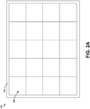
- FIG. 2A illustrates a top view of a solar cell array 130, according to an example.
- the solar cell array 130 includes a plurality of solar cell modules 100, where each of the plurality of solar cell modules 100 includes the features of the solar cell module 100 described above in relation to Figures 1A-1B .
- the solar cell array 130 further includes a panel 132 coupled to the laminate substrate 102 of each of the plurality of solar cell modules 100.
- the panel 132 provides a surface on which to secure the plurality of solar cell modules 100, as well as a power bus to receive power from the second contact pad 112. Adjacent solar cell modules of the plurality of solar cell modules 100 abut one another such that there is not a gap therebetween.
- Such an arrangement provides a more densely packed modular solar cell array 130, which increases efficiency, improves power density, and improves the overall performance of the solar cell array 130.
- a single coverglass 122 is provided over the multiple solar cell modules 100 of the solar cell array 130, as shown in Figure 2B .
- a separate coverglass 122 covers each individual solar cell module 100.
- the coverglass 122 covers two or more solar cell modules 100 of the solar cell array 130. Such arrangements are each possible due to the top surface 140 of the solar cell array 130 being substantially flat.
- the arrangement described above with a substantially flat top surface of the solar cell modules 100 and a corresponding substantially flat top surface of the solar cell array 130 provides a variety of advantages over solar cell modules with protruding features.
- flat solar cell module surfaces make such solar cell modules compatible with both folded and rolled array stowage, so they are able to fit into a smaller stowage volume inside a launch vehicle, without the need to allow for static or dynamic clearances for protruding components which typically complicate traditional flat panel array design.
- protruding components of traditional arrangements limit the power per unit stowage volume (W/m 3 ) capability, so the flat surface of the solar cell modules 100 described herein provides a benefit of a more efficient solar cell system.
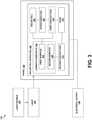
- FIG 3 is an illustration of a solar cell array 130 in the form of a functional block diagram.
- the solar cell array 130 includes a panel 132 with one or more solar cell modules 100 positioned thereon.
- the panel 132 is rigid.
- the panel 132 is flexible, such as a mesh backing.
- the one or more solar cell modules 100 are series-connected in a line, e.g., from top to bottom in each column of solar cell modules 100.
- each column of solar cell modules 100 terminates in a metal strip at the top and/or bottom of the column, and multiple columns are connected together at the top and/or bottom of each column with a wire.
- the solar cell modules 100 is series-connected in a line, e.g., from left to right in each row of solar cell modules 100.
- each row of solar cell modules 100 are terminated in a metal strip at the left and/or right of the row, and multiple rows are connected together at the left and/or right of each row with a wire.
- Each of the solar cell modules 100 absorbs light 134 from a light source 136 and generates an electrical output 138 in response thereto.
- the solar cell module 100 and corresponding solar cell array 130 described herein eliminates the need for manual wrapping or feeding of the wires, and instead uses the combination of the interconnects 120, the first contact pad 110, the vias 114, and the second contact pad 112 to transfer power from the solar cell 108 on the front side of the solar cell module 100 to output wiring 113 on the back side of the solar cell module 100.
- Each of these components can be manufactured and assembled autonomously, thereby reducing cost and increasing precision of the solar cell module 100.
- the front side of the solar cell module includes raised portions corresponding to the areas where the wiring will pass from the front side of the solar cell module to the back side of the solar cell module.
- the traditional feed-though wiring solution creates a non-uniform front-side surface at the edges of the solar cell module, which is not preferred for certain desired application as discussed above.
- Figure 4 is a block diagram of an example of a method 200 for fabricating a solar cell module 100.
- Method 200 shown in Figure 4 presents an example of a method that could be used with any of the examples of the solar cell module 100 discussed above in relation to Figures 1A-3 , as examples.
- Method 200 includes one or more operations, functions, or actions as illustrated by one or more of blocks 202-210. Although the blocks are illustrated in a sequential order, these blocks may also be performed in parallel, and/or in a different order than those described herein. Also, the various blocks may be combined into fewer blocks, divided into additional blocks, and/or removed based upon the desired implementation.
- the method 200 includes positioning a solar cell 108 on a first surface 104 of a laminate substrate 102.
- a circuit bonding adhesive 126 is positioned between the solar cell 108 and the laminate substrate 102 to thereby secure the solar cell 108 to the laminate substrate 102.
- the circuit bonding adhesive 126 comprises a pressure sensitive adhesive tape.
- the method 200 includes positioning a first contact pad 110 on the first surface 104 of the laminate substrate 102 adjacent to the solar cell 108.
- the method 200 includes positioning a second contact pad 112 positioned on a second surface 106 of the laminate substrate 102.
- the first contact pad 110 and the second contact pad 112 each comprise a conducting material.
- the first contact pad 110 and the second contact pad 112 each comprise a copper material.
- the copper material comprises a cladding or a patterning on the first contact pad 110 and the second contact pad 112.
- such a cladding or a patterning is created autonomously without the need for manual intervention.
- the second contact pad 112 comprises a landing pad for connecting the solar cell module 100 to a backside harness or substrate insert.
- the second contact pad 112 comprises a trace pattern on the back of the laminate substrate 102 to replace wires for portions of harnessing.
- the second contact pad 112 is patterned with output wiring 113 to carry power captured by the solar cell 108 to other devices.
- the method 200 includes forming one or more vias 114 through the laminate substrate 102 to electrically connect the first contact pad 110 to the second contact pad 112.
- Each of the one or more vias 114 comprise a through hole 116 including an interior surface 118 that is plated with a metallic material to thereby electrically connect the first contact pad 110 to the second contact pad 112.
- the metallic material comprises copper, although other conductive materials are possible as well.
- the method 200 includes electrically coupling one or more interconnects 120 extending from the solar cell 108 to the first contact pad 110.
- the one or more interconnects 120 comprise a metal foil or other conductive material.
- the one or more interconnects 120 comprise an end tab that is welded, soldered, or conductively bonded to the first contact pad 110. In another example, the one or more interconnects 120 are welded, soldered, or conductively bonded directly to the first contact pad 110 without the presence of an end tab.
- the method 200 further includes positioning a coverglass 122 on a top surface of the solar cell 108.
- the method 200 further includes positioning a glass bonding adhesive 124 between the coverglass 122 and the solar cell 108, to thereby secure the coverglass 122 to the solar cell 108.
- a top surface of the solar cell 108 and a top surface of the first contact pad 110 define a top surface 128 of the solar cell module 100, and the top surface 128 of the solar cell module 100 is substantially flat.
- the solar cell module 100 and corresponding method of fabrication described herein eliminates the need for manual wrapping or feeding of the wires, and instead uses the combination of the interconnects 120, the first contact pad 110, the vias 114, and the second contact pad 112 to transfer power from the solar cell 108 on the front side of the solar cell module 100 to output wiring 113 on the back side of the solar cell module 100.
- Each of these components can be manufactured and assembled autonomously, thereby reducing cost and increasing precision of the solar cell module 100.
Landscapes
- Photovoltaic Devices (AREA)
- Life Sciences & Earth Sciences (AREA)
- Engineering & Computer Science (AREA)
- Sustainable Development (AREA)
- Sustainable Energy (AREA)
Abstract
Description
- The present disclosure is related generally to solar cell modules and more specifically to a feed-through wiring solution for a solar cell array comprising a plurality of solar cell modules.
- A solar array generally is comprised of multiple solar cell modules connected together to produce electric power. Wiring must be completed across the solar cell modules to carry power to other devices. Current methods for extracting current from individual solar cell modules and routing them to the power bus for the solar cell array involves either flexible tabs that extend from the edge of each solar cell module or wires that are welded or soldered to the traces at the front side of each solar cell module. Getting the power from the front to the back side of the solar cell modules thus typically involves either allocating a sufficient gap between solar cell modules to enable wrapping of the wires or the flexible tabs around to the back of the assembly or including feed-through holes in the assembly to pass the wires from the front to the back of the solar cell modules.
- Either of these options requires manual labor to execute the routing with a sufficient radius to avoid open joints due to thermal cycling stress. These wiring solutions also create a non-uniform front-side surface at the edges of the solar cell module, making it non-ideal for certain desired applications. Therefore, a solar module design that enables tighter packing of adjacent solar array modules and simplifies the array level assembly, while also providing a uniform front-side height profile may be desirable.
- In one aspect, the present disclosure provides a solar cell module. The solar cell module includes (a) a laminate substrate having a first surface and a second surface opposite the first surface, (b) a solar cell positioned on the first surface of the laminate substrate, (c) a first contact pad positioned on the first surface of the laminate substrate adjacent to the solar cell, (d) a second contact pad positioned on the second surface of the laminate substrate, (e) one or more vias positioned through the laminate substrate to electrically connect the first contact pad to the second contact pad, and (f) one or more interconnects extending from the solar cell and electrically coupling the solar cell to the first contact pad.
- In another aspect, the present disclosure provides a solar cell array. The solar cell array comprises (a) a plurality of solar cell modules, wherein each of the plurality of solar cell modules includes (i) a laminate substrate having a first surface and a second surface opposite the first surface, (ii) a solar cell positioned on the first surface of the laminate substrate, (iii) a first contact pad positioned on the first surface of the laminate substrate adjacent to the solar cell, (iv) a second contact pad positioned on the second surface of the laminate substrate, (v) one or more vias positioned through the laminate substrate to electrically connect the first contact pad to the second contact pad, (vi) one or more interconnects extending from the solar cell and electrically coupling the solar cell to the first contact pad, and (b) a panel coupled to the laminate substrate of each of the plurality of solar cell modules, wherein adjacent solar cell modules of the plurality of solar cell modules abut one another such that there is not a gap therebetween.
- In yet another aspect, a method for fabricating a solar cell module is described. The method includes (a) positioning a solar cell on a first surface of a laminate substrate, (b) positioning a first contact pad on the first surface of the laminate substrate adjacent to the solar cell, (c) positioning a second contact pad positioned on a second surface of the laminate substrate, (d) forming one or more vias through the laminate substrate to electrically connect the first contact pad to the second contact pad, and (e) electrically coupling one or more interconnects extending from the solar cell to the first contact pad.
- The features, functions, and advantages that have been discussed can be achieved independently in various examples or may be combined in yet other examples further details of which can be seen with reference to the following description and figures.
- The novel features believed characteristic of the illustrative examples are set forth in the appended claims. The illustrative examples, however, as well as a preferred mode of use, further objectives and descriptions thereof, will best be understood by reference to the following detailed description of an illustrative examples of the present disclosure when read in conjunction with the accompanying figures.
-
Figure 1A is a side cross-sectional view of a solar cell module, according to an example implementation. -
Figure 1B is a side cross-sectional view of another solar cell module, according to an example implementation. -
Figure 2A is a top view of a solar cell array, according to an example implementation. -
Figure 2B is a side cross-sectional view of the solar cell array ofFigure 2A , according to an example implementation. -
Figure 3 is an illustration of a solar cell array in the form of a functional block diagram, according to an example implementation. -
Figure 4 is a flowchart of an example method, according to an example implementation. - Disclosed examples will now be described more fully hereinafter with reference to the accompanying figures, in which some, but not all of the disclosed examples are shown. Indeed, several different examples may be provided and should not be construed as limited to the examples set forth herein. Rather, these examples are provided so that this disclosure will be thorough and complete and will fully convey the scope of the disclosure to those skilled in the art.
- In the following description, numerous specific details are set forth to provide a thorough understanding of the disclosed concepts, which may be practiced without some or all of these particulars. In other instances, details of known devices and/or processes have been omitted to avoid unnecessarily obscuring the disclosure. While some concepts will be described in conjunction with specific examples, it will be understood that these examples are not intended to be limiting.
- In
Figure 4 , the blocks represent operations and/or portions thereof and lines connecting the various blocks do not imply any particular order or dependency of the operations or portions thereof. It will be understood that not all dependencies among the various disclosed operations are necessarily represented.Figure 4 and the accompanying disclosure describing the operations of the method(s) set forth herein should not be interpreted as necessarily determining a sequence in which the operations are to be performed. Rather, although one illustrative order is indicated, it is to be understood that the sequence of the operations may be modified when appropriate. Accordingly, certain operations may be performed in a different order or simultaneously. Additionally, those skilled in the art will appreciate that not all operations described need be performed. - Unless otherwise indicated, the terms "first," "second," etc. are used herein merely as labels, and are not intended to impose ordinal, positional, or hierarchical requirements on the items to which these terms refer. Moreover, reference to, e.g., a "second" item does not require or preclude the existence of, e.g., a "first" or lower-numbered item, and/or, e.g., a "third" or higher-numbered item.
- Reference herein to "one example" means that one or more feature, structure, or characteristic described in connection with the example is included in at least one implementation. The phrase "one example" in various places in the specification may or may not be referring to the same example.
- As used herein, a system, apparatus, device, structure, article, element, component, or hardware "configured to" perform a specified function is indeed capable of performing the specified function without any alteration, rather than merely having potential to perform the specified function after further modification. In other words, the system, apparatus, structure, article, element, component, or hardware "configured to" perform a specified function is specifically selected, created, implemented, utilized, programmed, and/or designed for the purpose of performing the specified function. As used herein, "configured to" denotes existing characteristics of a system, apparatus, structure, article, element, component, or hardware which enable the system, apparatus, structure, article, element, component, or hardware to perform the specified function without further modification. For purposes of this disclosure, a system, apparatus, structure, article, element, component, or hardware described as being "configured to" perform a particular function may additionally or alternatively be described as being "adapted to" and/or as being "operative to" perform that function.
- As used herein, with respect to measurements, "substantially flat" means a surface without any features protruding therefrom.
- Unless otherwise specifically noted, elements depicted in the drawings are not necessarily drawn to scale.
- Illustrative, non-exhaustive examples, which may or may not be claimed, of the subject matter according the present disclosure are provided below.
- The present disclosure provides a solar cell module, a solar cell array comprising a plurality of solar cell modules, and methods of manufacturing thereof. In particular, the present disclosure provides a low profile, high packing factor, reduced manufacturing cost solution for collecting power from a modular solar cell or flexible array assembly. Replacing the traditional Kapton® polyimide film substrate with a thin laminate including a two-sided cladding/patterning of front-side landing pads and back-side wiring routes with one or more vias in place of feed-through locations can result in the elimination of the need to allocate either gaps for wrapped wires or tabs or front-side height clearance for traditional feed-through wire routing. The solar cell module design described herein also can result in the elimination of manufacturing costs and a difficultly in redundancy with either of the heritage approaches. Further, the design described herein can enable tighter packing of the adjacent solar array modules and can simplify the array level assembly, while providing a uniform front-side height profile. The ability to maintain a flat front-side profile, while eliminating both the gaps and labor required for flexible tab or wire wrapping to the backside provides competitive advantages at the solar cell array level in terms of cost, packing factor, and reliability.
- These and other improvements are described in more detail below. Implementations described below are for purposes of example. The implementations described below, as well as other implementations, may provide other improvements as well.
- With reference to the Figures,
Figure 1A is a side cross-sectional view of asolar cell module 100 according to an example. As shown inFigure 1A , thesolar cell module 100 includes alaminate substrate 102 having afirst surface 104 and asecond surface 106 opposite thefirst surface 104. A thickness of thelaminate substrate 102 ranges from about 3mm to about 5mm. In one example, thelaminate substrate 102 comprises a fiberglass printed circuit board insulator material. Thelaminate substrate 102 comprises an insulating material capable of withstanding the rigors of space. In the proposed 3mm to 5mm thickness, thelaminate substrate 102 is still reasonably flexible, making it compatible for integration into either a flexible modular array solution or as the top layer in a rigid modular array. In one example, thelaminate substrate 102 is flexible. Such an arrangement is used when thesolar cell module 100 described herein is utilized in a flexible modular array solution. In another example, thelaminate substrate 102 is rigid. Such an arrangement is used when thesolar cell module 100 described herein is utilized in a rigid modular array. As such, thesolar cell module 100 described herein can be used in a variety of types of solar cell arrays. - The
solar cell module 100 further includes asolar cell 108 positioned on thefirst surface 104 of thelaminate substrate 102. Thesolar cell 108 can take on a variety sizes and forms, and comprises any structure for absorbing light from a light source to generate an electrical output in response thereto. In one example, thesolar cell 108 comprises a single solar cell. In another example, thesolar cell 108 comprises a plurality of solar cells connected in series on thefirst surface 104 of thelaminate substrate 102, and thesolar cell 108 is one of the plurality of solar cells. - The
solar cell module 100 further includes afirst contact pad 110 positioned on thefirst surface 104 of thelaminate substrate 102 adjacent to thesolar cell 108, and asecond contact pad 112 positioned on thesecond surface 106 of thelaminate substrate 102. In one example, thefirst contact pad 110 and thesecond contact pad 112 each comprise a conducting material. In one particular example, thefirst contact pad 110 and thesecond contact pad 112 each comprise a copper material. In such an example, the copper material comprises a cladding or a patterning on thefirst contact pad 110 and thesecond contact pad 112. In one example, thesecond contact pad 112 comprises a landing pad for connecting thesolar cell module 100 to a backside harness or substrate insert. In another example, thesecond contact pad 112 comprises a trace pattern on the back of thelaminate substrate 102 to replace wires for portions of harnessing. In yet another example, thesecond contact pad 112 is patterned withoutput wiring 113 to carry power captured by thesolar cell 108 to other devices. - As further shown in
Figure 1A , thesolar cell module 100 further includes one ormore vias 114 positioned through thelaminate substrate 102 to electrically connect thefirst contact pad 110 to thesecond contact pad 112. In one example, each of the one ormore vias 114 comprise a throughhole 116 including aninterior surface 118 that is plated with a metallic material to thereby electrically connect thefirst contact pad 110 to thesecond contact pad 112. In one particular example, the metallic material comprises copper, although other conductive materials are possible as well. - The
solar cell module 100 further includes one ormore interconnects 120 extending from thesolar cell 108 and electrically coupling thesolar cell 108 to thefirst contact pad 110. The one ormore interconnects 120 comprise a metal foil or other conductive material. In one example, the one ormore interconnects 120 comprise an end tab that is welded, soldered, or conductively bonded to thefirst contact pad 110. In another example, the one ormore interconnects 120 are welded, soldered, or conductively bonded directly to thefirst contact pad 110 without the presence of an end tab. In any event, the one ormore interconnects 120 electrically connects thesolar cell 108 to thefirst contact pad 110. - In one example, as shown in
Figure 1A , thesolar cell module 100 further includes acoverglass 122 positioned on a top surface of thesolar cell 108. In such an example, thesolar cell module 100 further includes aglass bonding adhesive 124 positioned between thecoverglass 122 and thesolar cell 108. In another example, acircuit bonding adhesive 126 is positioned between thesolar cell 108 and thelaminate substrate 102. In one example, thecircuit bonding adhesive 126 comprises a pressure sensitive adhesive tape. As shown inFigure 1A , a top surface of thecoverglass 122 and a top surface of thefirst contact pad 110 define atop surface 128 of thesolar cell module 100. As shown inFigure 1A , thetop surface 128 of the solar cell module is substantially flat. As such,solar cell module 100 has no features that protrude from thetop surface 128 of thesolar cell module 100 higher than the surface of thesolar cell 108 itself. In the example shown inFigure 1A , thecoverglass 122 covers thesolar cell 108 but not thefirst contact pad 110. -
Figure 1B is a side cross-sectional view of another arrangement of thesolar cell module 100, according to an example implementation. An advantage of the arrangement of thesolar cell module 100 shown inFigures 1A-1B is that there are no wires with diameters that would typically rise above the top surface of thesolar cell 108. In traditional solar cell arrangements, this is not the case. Therefore, as shown inFigure 1B , thesolar cell module 100 provides a sufficiently flat front surface which lends itself to applications where it is desirable to bond a singlelarge coverglass 122 over the entiresolar cell module 100, thereby covering both thesolar cell 108 and thefirst contact pad 110. Further, such an arrangement enables asingle coverglass 122 to extend between adjacentsolar cell modules 100 of a solar cell array, as discussed in additional detail below. -
Figure 2A illustrates a top view of asolar cell array 130, according to an example. As shown inFigure 2A , thesolar cell array 130 includes a plurality ofsolar cell modules 100, where each of the plurality ofsolar cell modules 100 includes the features of thesolar cell module 100 described above in relation toFigures 1A-1B . Thesolar cell array 130 further includes apanel 132 coupled to thelaminate substrate 102 of each of the plurality ofsolar cell modules 100. Thepanel 132 provides a surface on which to secure the plurality ofsolar cell modules 100, as well as a power bus to receive power from thesecond contact pad 112. Adjacent solar cell modules of the plurality ofsolar cell modules 100 abut one another such that there is not a gap therebetween. Such an arrangement provides a more densely packed modularsolar cell array 130, which increases efficiency, improves power density, and improves the overall performance of thesolar cell array 130. -
Figure 2B illustrates a side cross-sectional view of thesolar cell array 130 ofFigure 2A , according to an example. As shown inFigure 2B , adjacent solar cell modules of the plurality ofsolar cell modules 100 abut one another such that there is not a gap therebetween. A top surface of thesolar cell 108 and a top surface of thefirst contact pad 110 define atop surface 128 of each of thesolar cell modules 100, and collectively atop surface 140 of thesolar cell array 130. As shown inFigure 2B , thetop surface 140 of thesolar cell array 130 is substantially flat. As such, thetop surface 140 of thesolar cell array 130 has no features that protrude from the top surface higher than the surface of thesolar cell 108 itself. In one example, asingle coverglass 122 is provided over the multiplesolar cell modules 100 of thesolar cell array 130, as shown inFigure 2B . In another example, aseparate coverglass 122 covers each individualsolar cell module 100. In yet another example, thecoverglass 122 covers two or moresolar cell modules 100 of thesolar cell array 130. Such arrangements are each possible due to thetop surface 140 of thesolar cell array 130 being substantially flat. - The arrangement described above with a substantially flat top surface of the
solar cell modules 100 and a corresponding substantially flat top surface of thesolar cell array 130 provides a variety of advantages over solar cell modules with protruding features. As an initial matter, flat solar cell module surfaces make such solar cell modules compatible with both folded and rolled array stowage, so they are able to fit into a smaller stowage volume inside a launch vehicle, without the need to allow for static or dynamic clearances for protruding components which typically complicate traditional flat panel array design. Further, protruding components of traditional arrangements limit the power per unit stowage volume (W/m3) capability, so the flat surface of thesolar cell modules 100 described herein provides a benefit of a more efficient solar cell system. Further still, the flat surface of thesolar cell modules 100 described herein enables compatibility with applications where - for either manufacturability/cost savings or mission environment survivability reasons - it is desired to have asingle coverglass 122 applied over the entire module as shown inFigure 1B . -
Figure 3 is an illustration of asolar cell array 130 in the form of a functional block diagram. As shown inFigure 3 , thesolar cell array 130 includes apanel 132 with one or moresolar cell modules 100 positioned thereon. In one example, thepanel 132 is rigid. In another example, thepanel 132 is flexible, such as a mesh backing. The one or moresolar cell modules 100 are series-connected in a line, e.g., from top to bottom in each column ofsolar cell modules 100. In one example, each column ofsolar cell modules 100 terminates in a metal strip at the top and/or bottom of the column, and multiple columns are connected together at the top and/or bottom of each column with a wire. Alternatively, thesolar cell modules 100 is series-connected in a line, e.g., from left to right in each row ofsolar cell modules 100. In such an example, each row ofsolar cell modules 100 are terminated in a metal strip at the left and/or right of the row, and multiple rows are connected together at the left and/or right of each row with a wire. Each of thesolar cell modules 100 absorbs light 134 from alight source 136 and generates anelectrical output 138 in response thereto. - As discussed above, traditional methods for extracting current from individual solar cell modules involves either flexible tabs that extend from the edge of each solar cell module or wires that are welded or soldered to the traces at the front side of each solar cell module. Getting the power from the front to the back side of the solar cell modules thus typically involves either allocating a sufficient gap between solar cell modules to enable wrapping of the wires around the flexible tabs or including feed-through holes in the assembly to pass the wires from the front to the back of the solar cell modules.
- Either of these options requires manual labor to execute the routing of the wires either around the flexible tabs or through the feed-through holes. This manual labor step is time consuming, and thus expensive. The
solar cell module 100 and correspondingsolar cell array 130 described herein eliminates the need for manual wrapping or feeding of the wires, and instead uses the combination of theinterconnects 120, thefirst contact pad 110, thevias 114, and thesecond contact pad 112 to transfer power from thesolar cell 108 on the front side of thesolar cell module 100 tooutput wiring 113 on the back side of thesolar cell module 100. Each of these components can be manufactured and assembled autonomously, thereby reducing cost and increasing precision of thesolar cell module 100. - Further, in the case of the traditional flexible tab wiring solution, the existence of the flexible tabs creates a necessary gap (typically about 0.25 inches) between adjacent solar cell modules. As discussed above, the
solar cell module 100 and correspondingsolar cell array 130 described herein eliminate this gap between adjacentsolar cell modules 100. Such an arrangement provides a more densely packed modularsolar cell array 130, which increases efficiency, improves power density, and improves the overall performance of thesolar cell array 130. - Further still, in the case of the traditional feed-though wiring solution, the front side of the solar cell module includes raised portions corresponding to the areas where the wiring will pass from the front side of the solar cell module to the back side of the solar cell module. Thus, the traditional feed-though wiring solution creates a non-uniform front-side surface at the edges of the solar cell module, which is not preferred for certain desired application as discussed above.
-
Figure 4 is a block diagram of an example of amethod 200 for fabricating asolar cell module 100.Method 200 shown inFigure 4 presents an example of a method that could be used with any of the examples of thesolar cell module 100 discussed above in relation toFigures 1A-3 , as examples.Method 200 includes one or more operations, functions, or actions as illustrated by one or more of blocks 202-210. Although the blocks are illustrated in a sequential order, these blocks may also be performed in parallel, and/or in a different order than those described herein. Also, the various blocks may be combined into fewer blocks, divided into additional blocks, and/or removed based upon the desired implementation. - Initially, at
block 202, themethod 200 includes positioning asolar cell 108 on afirst surface 104 of alaminate substrate 102. In one example, acircuit bonding adhesive 126 is positioned between thesolar cell 108 and thelaminate substrate 102 to thereby secure thesolar cell 108 to thelaminate substrate 102. In one example, thecircuit bonding adhesive 126 comprises a pressure sensitive adhesive tape. Atblock 204, themethod 200 includes positioning afirst contact pad 110 on thefirst surface 104 of thelaminate substrate 102 adjacent to thesolar cell 108. Atblock 206, themethod 200 includes positioning asecond contact pad 112 positioned on asecond surface 106 of thelaminate substrate 102. Thefirst contact pad 110 and thesecond contact pad 112 each comprise a conducting material. In one particular example, thefirst contact pad 110 and thesecond contact pad 112 each comprise a copper material. In such an example, the copper material comprises a cladding or a patterning on thefirst contact pad 110 and thesecond contact pad 112. In one example, such a cladding or a patterning is created autonomously without the need for manual intervention. In one example, thesecond contact pad 112 comprises a landing pad for connecting thesolar cell module 100 to a backside harness or substrate insert. In another example, thesecond contact pad 112 comprises a trace pattern on the back of thelaminate substrate 102 to replace wires for portions of harnessing. In yet another example, thesecond contact pad 112 is patterned withoutput wiring 113 to carry power captured by thesolar cell 108 to other devices. - At
block 208, themethod 200 includes forming one ormore vias 114 through thelaminate substrate 102 to electrically connect thefirst contact pad 110 to thesecond contact pad 112. Each of the one ormore vias 114 comprise a throughhole 116 including aninterior surface 118 that is plated with a metallic material to thereby electrically connect thefirst contact pad 110 to thesecond contact pad 112. In one particular example, the metallic material comprises copper, although other conductive materials are possible as well. Atblock 210, themethod 200 includes electrically coupling one ormore interconnects 120 extending from thesolar cell 108 to thefirst contact pad 110. The one ormore interconnects 120 comprise a metal foil or other conductive material. In one example, the one ormore interconnects 120 comprise an end tab that is welded, soldered, or conductively bonded to thefirst contact pad 110. In another example, the one ormore interconnects 120 are welded, soldered, or conductively bonded directly to thefirst contact pad 110 without the presence of an end tab. - In one example, the
method 200 further includes positioning acoverglass 122 on a top surface of thesolar cell 108. In such an example, themethod 200 further includes positioning aglass bonding adhesive 124 between thecoverglass 122 and thesolar cell 108, to thereby secure thecoverglass 122 to thesolar cell 108. Further, in such an example, a top surface of thesolar cell 108 and a top surface of thefirst contact pad 110 define atop surface 128 of thesolar cell module 100, and thetop surface 128 of thesolar cell module 100 is substantially flat. - As discussed above, traditional wiring solutions require manual labor to execute the routing of the wires either around flexible tabs or through feed-through holes to thereby enable power to run from the front side to the back side of the solar cell module. This manual labor step is time consuming, and thus expensive. The
solar cell module 100 and corresponding method of fabrication described herein eliminates the need for manual wrapping or feeding of the wires, and instead uses the combination of theinterconnects 120, thefirst contact pad 110, thevias 114, and thesecond contact pad 112 to transfer power from thesolar cell 108 on the front side of thesolar cell module 100 tooutput wiring 113 on the back side of thesolar cell module 100. Each of these components can be manufactured and assembled autonomously, thereby reducing cost and increasing precision of thesolar cell module 100. - Further, the disclosure comprise examples according to the following clauses:
- Clause 1. A solar cell module, comprising: a laminate substrate having a first surface and a second surface opposite the first surface; a solar cell positioned on the first surface of the laminate substrate; a first contact pad positioned on the first surface of the laminate substrate adjacent to the solar cell; a second contact pad positioned on the second surface of the laminate substrate; one or more vias positioned through the laminate substrate to electrically connect the first contact pad to the second contact pad; and one or more interconnects extending from the solar cell and electrically coupling the solar cell to the first contact pad.
- Clause 2. The solar cell module of Clause 1, further comprising: a coverglass positioned on a top surface of the solar cell.
- Clause 3. The solar cell module of Clause 2, further comprising: a glass bonding adhesive positioned between the coverglass and the solar cell; and a circuit bonding adhesive positioned between the solar cell and the laminate substrate.
- Clause 4. The solar cell module of any of Clauses 1-3, wherein a top surface of the solar cell and a top surface of the first contact pad define a top surface of the solar cell module, and
- wherein the top surface of the solar cell module is substantially flat.
- Clause 5. The solar cell module of any of Clauses 1-4, wherein a thickness of the laminate substrate ranges from about 3mm to about 5mm.
- Clause 6. The solar cell module of any of Clauses 1-5, wherein the laminate substrate comprises a fiberglass printed circuit board insulator material.
- Clause 7. The solar cell module of any of Clauses 1-6, wherein the first contact pad and the second contact pad comprise a copper material.
- Clause 8. The solar cell module of Clause 7, wherein the copper material comprises a cladding or a patterning on the first contact pad and the second contact pad.
- Clause 9. The solar cell module of any of Clauses 1-8, further comprising a plurality of solar cells connected in series on the first surface of the laminate substrate, wherein the solar cell is one of the plurality of solar cells.
- Clause 10. The solar cell module of any of Clauses 1-9, wherein the one or more interconnects are welded, soldered, or conductively bonded directly to the first contact pad.
- Clause 11. The solar cell module of any of Clauses 1-10, wherein the one or more interconnects comprise an end tab that is welded, soldered, or conductively bonded to the first contact pad.
- Clause 12. The solar cell module of any of Clauses 1-11, wherein each of the one or more vias comprise a through hole including an interior surface that is plated with a metallic material to thereby electrically connect the first contact pad to the second contact pad.
- Clause 13. The solar cell module of any of Clauses 1-12, wherein the laminate substrate is flexible.
- Clause 14. The solar cell module of any of Clauses 1-13, wherein the laminate substrate is rigid.
- Clause 15. A solar cell array, comprising: a plurality of solar cell modules, wherein each of the plurality of solar cell modules includes: a laminate substrate having a first surface and a second surface opposite the first surface; a solar cell positioned on the first surface of the laminate substrate; a first contact pad positioned on the first surface of the laminate substrate adjacent to the solar cell; a second contact pad positioned on the second surface of the laminate substrate; one or more vias positioned through the laminate substrate to electrically connect the first contact pad to the second contact pad; and one or more interconnects extending from the solar cell and electrically coupling the solar cell to the first contact pad; and a panel coupled to the laminate substrate of each of the plurality of solar cell modules, wherein adjacent solar cell modules of the plurality of solar cell modules abut one another such that there is not a gap therebetween.
- Clause 16. The solar cell array of Clause 15, wherein each of the plurality of solar cell modules includes a coverglass positioned on a top surface of the solar cell.
- Clause 17. The solar cell array of Clause 15 or 16, wherein a top surface of the solar cell and
- a top surface of the first contact pad define a top surface of the solar cell array, and wherein the top surface of the solar cell array is substantially flat.
- Clause 18. A method for fabricating a solar cell module, comprising: positioning a solar cell on a first surface of a laminate substrate; positioning a first contact pad on the first surface of the laminate substrate adjacent to the solar cell; positioning a second contact pad positioned on a second surface of the laminate substrate; forming one or more vias through the laminate substrate to electrically connect the first contact pad to the second contact pad; and electrically coupling one or more interconnects extending from the solar cell to the first contact pad.
- Clause 19. The method of Clause 18, further comprising: positioning a coverglass on a top surface of the solar cell.
- Clause 20. The method of Clause 18 or 19, wherein a top surface of the solar cell and a top surface of the first contact pad define a top surface of the solar cell module, and wherein the top surface of the solar cell module is substantially flat.
- It should be understood that arrangements described herein are for purposes of example only. As such, those skilled in the art will appreciate that other arrangements and other elements (e.g. machines, interfaces, functions, orders, and groupings of functions, etc.) can be used instead, and some elements may be omitted altogether according to the desired results. Further, many of the elements that are described are functional entities that may be implemented as discrete or distributed components or in conjunction with other components, in any suitable combination and location, or other structural elements described as independent structures may be combined.
- The description of the different advantageous arrangements has been presented for purposes of illustration and description, and is not intended to be exhaustive or limited to the examples in the form disclosed. Many modifications and variations will be apparent to those of ordinary skill in the art. Further, different advantageous examples may provide different advantages as compared to other advantageous examples. The example or examples selected are chosen and described in order to best explain the principles of the examples, the practical application, and to enable others of ordinary skill in the art to understand the disclosure for various examples with various modifications as are suited to the particular use contemplated.
Claims (15)
- A solar cell module (100), comprising:a laminate substrate (102) having a first surface (104) and a second surface (106) opposite the first surface (104);a solar cell (108) positioned on the first surface (104) of the laminate substrate (102);a first contact pad (110) positioned on the first surface (104) of the laminate substrate (102) adjacent to the solar cell (108);a second contact pad (112) positioned on the second surface (106) of the laminate substrate (102);one or more vias (114) positioned through the laminate substrate (102) to electronically connect the first contact pad (110) to the second contact pad (112); andone or more interconnects (120) extending from the solar cell (108) and electronically coupling the solar cell (108) to the first contact pad (110).
- The solar cell module (100) of claim 1, further comprising:a coverglass (122) positioned on a top surface of the solar cell (108),the cell module optionally further comprising:a glass bonding adhesive (124) positioned between the coverglass (122) and the solar cell (108); anda circuit bonding adhesive (126) positioned between the solar cell (108) and the laminate substrate (102).
- The solar cell module (100) of claim 2, wherein a top surface of the coverglass (122) and a top surface of the first contact pad (110) define a top surface (128) of the solar cell module (100), and wherein the top surface (128) of the solar cell module (100) is substantially flat.
- The solar cell module (100) of any of claims 1-3, wherein a thickness of the laminate substrate (102) ranges from about 3mm to about 5mm.
- The solar cell module (100) of any of claims 1-4, wherein the laminate substrate (102) comprises a fiberglass printed circuit board insulator material.
- The solar cell module (100) of any of claims 1-5, wherein the first contact pad (110) and the second contact pad (112) comprise a copper material, wherein the copper material optionally comprises a cladding or a patterning on the first contact pad (110) and the second contact pad (112).
- The solar cell module (100) of any of claims 1-6, further comprising a plurality of solar cells connected in series on the first surface (104) of the laminate substrate (102), wherein the solar cell (108) is one of the plurality of solar cells.
- The solar cell module (100) of any of claims 1-7, wherein the one or more interconnects (120) are welded, soldered, or conductively bonded directly to the first contact pad (110), and/or wherein the one or more interconnects (120) optionally comprise an end tab that is welded, soldered, or conductively bonded to the first contact pad (110).
- The solar cell module (100) of any of claims 1-8, wherein each of the one or more vias (114) comprise a through hole (116) including an interior surface (118) that is plated with a metallic material to thereby electronically connect the first contact pad (110) to the second contact pad (112).
- The solar cell module (100) of any of claims 1-9, wherein the laminate substrate (102) is flexible or is rigid.
- A solar cell array (150), comprising:a plurality of solar cell modules (100), wherein each of the plurality of solar cell modules (100) includes:a laminate substrate (102) having a first surface (104) and a second surface (106) opposite the first surface (104);a solar cell (108) positioned on the first surface (104) of the laminate substrate (102);a first contact pad (110) positioned on the first surface (104) of the laminate substrate (102) adjacent to the solar cell (108);a second contact pad (112) positioned on the second surface (106) of the laminate substrate (102);one or more vias (114) positioned through the laminate substrate (102) to electronically connect the first contact pad (110) to the second contact pad (112); andone or more interconnects (116) extending from the solar cell (108) and electronically coupling the solar cell (108) to the first contact pad (110); anda panel (132) coupled to the laminate substrate (102) of each of the plurality of solar cell modules (100), wherein adjacent solar cell modules (100) of the plurality of solar cell modules (100) abut one another such that there is not a gap therebetween.
- The solar cell array (150) of claim 11, wherein each of the plurality of solar cell modules (100) includes a coverglass (122) positioned on a top surface of the solar cell (108), wherein a top surface of the coverglass (122) and a top surface of the first contact pad (110) define a top surface (128) of the solar cell array (150), and wherein the top surface (128) of the solar cell array (150) is substantially flat.
- The solar cell array (150) of claim 11 or 12, wherein the first contact pad (110) and the second contact pad (112) of each of the plurality of solar cell modules (100) comprise a copper material that is a cladding or a patterning on the first contact pad (110) and the second contact pad (112).
- A method (200) for fabricating a solar cell module (100), comprising:positioning (202) a solar cell (108) on a first surface (104) of a laminate substrate (102);positioning (204) a first contact pad (110) on the first surface (104) of the laminate substrate (102) adjacent to the solar cell (108);positioning (206) a second contact pad (112) positioned on a second surface (106) of the laminate substrate (102);forming (208) one or more vias (114) through the laminate substrate (102) to electronically connect the first contact pad (110) to the second contact pad (112); andelectronically coupling (210) one or more interconnects (120) extending from the solar cell (108) to the first contact pad (110).
- The method (200) of claim 14, further comprising:positioning a coverglass (122) on a top surface of the solar cell (108), wherein a top surface of the coverglass (122) and a top surface of the first contact pad (100) optionally define a top surface (128) of the solar cell module (100), and wherein the top surface (128) of the solar cell module (100) is substantially flat.
Priority Applications (1)
| Application Number | Priority Date | Filing Date | Title |
|---|---|---|---|
| EP23197671.3A EP4273939A3 (en) | 2020-08-11 | 2021-06-25 | Feed-through wiring solution for solar cell modules |
Applications Claiming Priority (2)
| Application Number | Priority Date | Filing Date | Title |
|---|---|---|---|
| US202063064088P | 2020-08-11 | 2020-08-11 | |
| US17/348,192 US12040414B2 (en) | 2020-08-11 | 2021-06-15 | Feed-through wiring solution for solar cell modules |
Related Child Applications (2)
| Application Number | Title | Priority Date | Filing Date |
|---|---|---|---|
| EP23197671.3A Division-Into EP4273939A3 (en) | 2020-08-11 | 2021-06-25 | Feed-through wiring solution for solar cell modules |
| EP23197671.3A Division EP4273939A3 (en) | 2020-08-11 | 2021-06-25 | Feed-through wiring solution for solar cell modules |
Publications (2)
| Publication Number | Publication Date |
|---|---|
| EP3955318A1 true EP3955318A1 (en) | 2022-02-16 |
| EP3955318B1 EP3955318B1 (en) | 2024-08-07 |
Family
ID=76623933
Family Applications (2)
| Application Number | Title | Priority Date | Filing Date |
|---|---|---|---|
| EP23197671.3A Pending EP4273939A3 (en) | 2020-08-11 | 2021-06-25 | Feed-through wiring solution for solar cell modules |
| EP21181717.6A Active EP3955318B1 (en) | 2020-08-11 | 2021-06-25 | Feed-through wiring solution for solar cell modules |
Family Applications Before (1)
| Application Number | Title | Priority Date | Filing Date |
|---|---|---|---|
| EP23197671.3A Pending EP4273939A3 (en) | 2020-08-11 | 2021-06-25 | Feed-through wiring solution for solar cell modules |
Country Status (5)
| Country | Link |
|---|---|
| US (1) | US12040414B2 (en) |
| EP (2) | EP4273939A3 (en) |
| JP (1) | JP7834438B2 (en) |
| CA (1) | CA3124504A1 (en) |
| ES (1) | ES2992420T3 (en) |
Families Citing this family (1)
| Publication number | Priority date | Publication date | Assignee | Title |
|---|---|---|---|---|
| CN116151159A (en) * | 2022-12-16 | 2023-05-23 | 中电科蓝天科技股份有限公司 | An integrated design method for satellite solar cell array confluence module |
Citations (4)
| Publication number | Priority date | Publication date | Assignee | Title |
|---|---|---|---|---|
| US20130323526A1 (en) * | 2012-05-29 | 2013-12-05 | Essence Solar Solutions Ltd. | Self aligning soldering |
| US20180108794A1 (en) * | 2014-04-07 | 2018-04-19 | Solaero Technologies Corp. | Space-qualified solar cell module with interconnection of neighboring solar cells on a common back plane |
| US10193493B2 (en) * | 2016-09-20 | 2019-01-29 | Intel Corporation | Multi-surface solar cell packaging for self-powered electronic devices |
| US10416425B2 (en) * | 2009-02-09 | 2019-09-17 | X-Celeprint Limited | Concentrator-type photovoltaic (CPV) modules, receiver and sub-receivers and methods of forming same |
Family Cites Families (26)
| Publication number | Priority date | Publication date | Assignee | Title |
|---|---|---|---|---|
| JPS6242469A (en) * | 1985-08-19 | 1987-02-24 | Sharp Corp | Solar array |
| US4773945A (en) * | 1987-09-14 | 1988-09-27 | Ga Technologies, Inc. | Solar cell with low infra-red absorption and method of manufacture |
| JPH08298334A (en) * | 1995-04-26 | 1996-11-12 | Mitsubishi Electric Corp | Solar cell plate |
| JP3133269B2 (en) * | 1997-03-03 | 2001-02-05 | 三洋電機株式会社 | Solar panel |
| JPH11112008A (en) * | 1997-10-03 | 1999-04-23 | Sharp Corp | Solar cell module |
| US6313396B1 (en) * | 2000-05-22 | 2001-11-06 | The Boeing Company | Lightweight solar module and method of fabrication |
| JP4092890B2 (en) * | 2001-05-31 | 2008-05-28 | 株式会社日立製作所 | Multi-chip module |
| GB2388744A (en) * | 2002-03-01 | 2003-11-19 | Btg Int Ltd | An RFID tag |
| JP2005340362A (en) * | 2004-05-25 | 2005-12-08 | Sharp Corp | Solar cell and solar cell module |
| JP5384819B2 (en) * | 2007-12-07 | 2014-01-08 | 日本特殊陶業株式会社 | Opto-electric hybrid package, opto-electric hybrid module |
| JP2009266958A (en) * | 2008-04-23 | 2009-11-12 | Sharp Corp | Solar battery module |
| US9450126B1 (en) | 2010-06-18 | 2016-09-20 | The Boeing Company | Solar cell module |
| JP2012186314A (en) * | 2011-03-04 | 2012-09-27 | Sharp Corp | Solar battery module |
| JP2013143401A (en) * | 2012-01-06 | 2013-07-22 | Sharp Corp | Solar cell module and manufacturing method of the same |
| US20150206997A1 (en) * | 2012-04-06 | 2015-07-23 | Solar Junction Corporation | Multi-junction solar cells with recessed through-substrate vias |
| US20140034127A1 (en) * | 2012-07-31 | 2014-02-06 | Semprius, Inc. | Surface-mountable lens cradles and interconnection structures for concentrator-type photovoltaic devices |
| CN203277425U (en) * | 2013-01-25 | 2013-11-06 | 纳幕尔杜邦公司 | Integrated backplane and back-contact photovoltaic modules |
| CN105229795A (en) * | 2013-03-14 | 2016-01-06 | 森普留斯公司 | For the high-efficiency solar receiver comprising stacking solar cell of condensation photovoltaic |
| CN105336749B (en) * | 2015-10-14 | 2018-05-08 | 天津三安光电有限公司 | Upside-down mounting multijunction solar cell chip of integrated bypass diode and preparation method thereof |
| WO2017201133A1 (en) * | 2016-05-17 | 2017-11-23 | SolaBlock LLC | Solar tile system |
| US10763383B2 (en) * | 2016-09-14 | 2020-09-01 | The Boeing Company | Nano-metal connections for a solar cell array |
| WO2018150894A1 (en) * | 2017-02-16 | 2018-08-23 | パナソニックIpマネジメント株式会社 | Solar cell module |
| US12244265B2 (en) | 2018-03-28 | 2025-03-04 | The Boeing Company | Wiring for a rigid panel solar array |
| EP3573110A1 (en) * | 2018-05-25 | 2019-11-27 | (CNBM) Bengbu Design & Research Institute for Glass Industry Co., Ltd. | Solar module with increased aperture |
| JP3220532U (en) * | 2018-12-18 | 2019-03-14 | 有限会社ディアックス | Beam lead type solar cell |
| US11062976B2 (en) * | 2019-05-03 | 2021-07-13 | International Business Machines Corporation | Functional stiffener that enables land grid array interconnections and power decoupling |
-
2021
- 2021-06-15 US US17/348,192 patent/US12040414B2/en active Active
- 2021-06-25 EP EP23197671.3A patent/EP4273939A3/en active Pending
- 2021-06-25 EP EP21181717.6A patent/EP3955318B1/en active Active
- 2021-06-25 ES ES21181717T patent/ES2992420T3/en active Active
- 2021-07-13 CA CA3124504A patent/CA3124504A1/en active Pending
- 2021-08-10 JP JP2021130657A patent/JP7834438B2/en active Active
Patent Citations (4)
| Publication number | Priority date | Publication date | Assignee | Title |
|---|---|---|---|---|
| US10416425B2 (en) * | 2009-02-09 | 2019-09-17 | X-Celeprint Limited | Concentrator-type photovoltaic (CPV) modules, receiver and sub-receivers and methods of forming same |
| US20130323526A1 (en) * | 2012-05-29 | 2013-12-05 | Essence Solar Solutions Ltd. | Self aligning soldering |
| US20180108794A1 (en) * | 2014-04-07 | 2018-04-19 | Solaero Technologies Corp. | Space-qualified solar cell module with interconnection of neighboring solar cells on a common back plane |
| US10193493B2 (en) * | 2016-09-20 | 2019-01-29 | Intel Corporation | Multi-surface solar cell packaging for self-powered electronic devices |
Also Published As
| Publication number | Publication date |
|---|---|
| CA3124504A1 (en) | 2022-02-11 |
| JP7834438B2 (en) | 2026-03-24 |
| EP3955318B1 (en) | 2024-08-07 |
| EP4273939A3 (en) | 2024-01-10 |
| JP2022042966A (en) | 2022-03-15 |
| EP4273939A2 (en) | 2023-11-08 |
| US12040414B2 (en) | 2024-07-16 |
| US20220052209A1 (en) | 2022-02-17 |
| ES2992420T3 (en) | 2024-12-12 |
Similar Documents
| Publication | Publication Date | Title |
|---|---|---|
| US9368651B2 (en) | Buss bar strip | |
| JP7511328B2 (en) | Wiring for Rigid Panel Solar Arrays | |
| US11967923B2 (en) | Single sheet foldout solar array | |
| EP4273940B1 (en) | Power routing module for a solar cell array | |
| US20140212695A1 (en) | Flexible printed circuit as high voltage interconnect in battery modules | |
| JP2001332753A (en) | Light weight solar cell module and method of manufacturing the same | |
| EP3907766A1 (en) | Solar cell array connections using corner conductors | |
| US20180076346A1 (en) | Solar cell array connections using corner conductors | |
| WO2013011748A1 (en) | Battery module | |
| US12040414B2 (en) | Feed-through wiring solution for solar cell modules | |
| US9450126B1 (en) | Solar cell module | |
| US11552344B2 (en) | Flex foil substrate connector for sensing battery voltage and temperature | |
| US20230021466A1 (en) | Photovoltaic module and flexible satellite solar generator | |
| JP2004327698A (en) | Solar cell module and method of manufacturing the same | |
| JP2008235819A (en) | Solar cell module | |
| JP2024538648A (en) | Sampling device, battery management system and vehicle | |
| CN102246322B (en) | Method for producing a photovoltaic module and photovoltaic module | |
| CN114446513A (en) | Flexible flat cable and laminated busbar comprising same | |
| US20240332644A1 (en) | Battery pack and method of manufacturing the same | |
| CN223297762U (en) | A cell data acquisition circuit connection component for a hybrid battery module |
Legal Events
| Date | Code | Title | Description |
|---|---|---|---|
| PUAI | Public reference made under article 153(3) epc to a published international application that has entered the european phase |
Free format text: ORIGINAL CODE: 0009012 |
|
| STAA | Information on the status of an ep patent application or granted ep patent |
Free format text: STATUS: THE APPLICATION HAS BEEN PUBLISHED |
|
| AK | Designated contracting states |
Kind code of ref document: A1 Designated state(s): AL AT BE BG CH CY CZ DE DK EE ES FI FR GB GR HR HU IE IS IT LI LT LU LV MC MK MT NL NO PL PT RO RS SE SI SK SM TR |
|
| STAA | Information on the status of an ep patent application or granted ep patent |
Free format text: STATUS: REQUEST FOR EXAMINATION WAS MADE |
|
| 17P | Request for examination filed |
Effective date: 20220721 |
|
| RBV | Designated contracting states (corrected) |
Designated state(s): AL AT BE BG CH CY CZ DE DK EE ES FI FR GB GR HR HU IE IS IT LI LT LU LV MC MK MT NL NO PL PT RO RS SE SI SK SM TR |
|
| GRAP | Despatch of communication of intention to grant a patent |
Free format text: ORIGINAL CODE: EPIDOSNIGR1 |
|
| STAA | Information on the status of an ep patent application or granted ep patent |
Free format text: STATUS: GRANT OF PATENT IS INTENDED |
|
| RAP3 | Party data changed (applicant data changed or rights of an application transferred) |
Owner name: THE BOEING COMPANY |
|
| INTG | Intention to grant announced |
Effective date: 20230302 |
|
| P01 | Opt-out of the competence of the unified patent court (upc) registered |
Effective date: 20230516 |
|
| GRAJ | Information related to disapproval of communication of intention to grant by the applicant or resumption of examination proceedings by the epo deleted |
Free format text: ORIGINAL CODE: EPIDOSDIGR1 |
|
| STAA | Information on the status of an ep patent application or granted ep patent |
Free format text: STATUS: REQUEST FOR EXAMINATION WAS MADE |
|
| STAA | Information on the status of an ep patent application or granted ep patent |
Free format text: STATUS: EXAMINATION IS IN PROGRESS |
|
| 17Q | First examination report despatched |
Effective date: 20230714 |
|
| INTC | Intention to grant announced (deleted) | ||
| GRAP | Despatch of communication of intention to grant a patent |
Free format text: ORIGINAL CODE: EPIDOSNIGR1 |
|
| STAA | Information on the status of an ep patent application or granted ep patent |
Free format text: STATUS: GRANT OF PATENT IS INTENDED |
|
| INTG | Intention to grant announced |
Effective date: 20240207 |
|
| GRAS | Grant fee paid |
Free format text: ORIGINAL CODE: EPIDOSNIGR3 |
|
| GRAA | (expected) grant |
Free format text: ORIGINAL CODE: 0009210 |
|
| STAA | Information on the status of an ep patent application or granted ep patent |
Free format text: STATUS: THE PATENT HAS BEEN GRANTED |
|
| AK | Designated contracting states |
Kind code of ref document: B1 Designated state(s): AL AT BE BG CH CY CZ DE DK EE ES FI FR GB GR HR HU IE IS IT LI LT LU LV MC MK MT NL NO PL PT RO RS SE SI SK SM TR |
|
| REG | Reference to a national code |
Ref country code: GB Ref legal event code: FG4D |
|
| REG | Reference to a national code |
Ref country code: CH Ref legal event code: EP |
|
| REG | Reference to a national code |
Ref country code: IE Ref legal event code: FG4D |
|
| REG | Reference to a national code |
Ref country code: DE Ref legal event code: R096 Ref document number: 602021016701 Country of ref document: DE |
|
| REG | Reference to a national code |
Ref country code: NL Ref legal event code: FP |
|
| REG | Reference to a national code |
Ref country code: DE Ref legal event code: R079 Ref document number: 602021016701 Country of ref document: DE Free format text: PREVIOUS MAIN CLASS: H01L0031020000 Ipc: H10F0077000000 |
|
| REG | Reference to a national code |
Ref country code: LT Ref legal event code: MG9D |
|
| REG | Reference to a national code |
Ref country code: ES Ref legal event code: FG2A Ref document number: 2992420 Country of ref document: ES Kind code of ref document: T3 Effective date: 20241212 |
|
| PG25 | Lapsed in a contracting state [announced via postgrant information from national office to epo] |
Ref country code: NO Free format text: LAPSE BECAUSE OF FAILURE TO SUBMIT A TRANSLATION OF THE DESCRIPTION OR TO PAY THE FEE WITHIN THE PRESCRIBED TIME-LIMIT Effective date: 20241107 |
|
| REG | Reference to a national code |
Ref country code: AT Ref legal event code: MK05 Ref document number: 1711945 Country of ref document: AT Kind code of ref document: T Effective date: 20240807 |
|
| PG25 | Lapsed in a contracting state [announced via postgrant information from national office to epo] |
Ref country code: PL Free format text: LAPSE BECAUSE OF FAILURE TO SUBMIT A TRANSLATION OF THE DESCRIPTION OR TO PAY THE FEE WITHIN THE PRESCRIBED TIME-LIMIT Effective date: 20240807 Ref country code: GR Free format text: LAPSE BECAUSE OF FAILURE TO SUBMIT A TRANSLATION OF THE DESCRIPTION OR TO PAY THE FEE WITHIN THE PRESCRIBED TIME-LIMIT Effective date: 20241108 Ref country code: PT Free format text: LAPSE BECAUSE OF FAILURE TO SUBMIT A TRANSLATION OF THE DESCRIPTION OR TO PAY THE FEE WITHIN THE PRESCRIBED TIME-LIMIT Effective date: 20241209 Ref country code: FI Free format text: LAPSE BECAUSE OF FAILURE TO SUBMIT A TRANSLATION OF THE DESCRIPTION OR TO PAY THE FEE WITHIN THE PRESCRIBED TIME-LIMIT Effective date: 20240807 |
|
| PG25 | Lapsed in a contracting state [announced via postgrant information from national office to epo] |
Ref country code: BG Free format text: LAPSE BECAUSE OF FAILURE TO SUBMIT A TRANSLATION OF THE DESCRIPTION OR TO PAY THE FEE WITHIN THE PRESCRIBED TIME-LIMIT Effective date: 20240807 |
|
| PG25 | Lapsed in a contracting state [announced via postgrant information from national office to epo] |
Ref country code: LV Free format text: LAPSE BECAUSE OF FAILURE TO SUBMIT A TRANSLATION OF THE DESCRIPTION OR TO PAY THE FEE WITHIN THE PRESCRIBED TIME-LIMIT Effective date: 20240807 |
|
| PG25 | Lapsed in a contracting state [announced via postgrant information from national office to epo] |
Ref country code: AT Free format text: LAPSE BECAUSE OF FAILURE TO SUBMIT A TRANSLATION OF THE DESCRIPTION OR TO PAY THE FEE WITHIN THE PRESCRIBED TIME-LIMIT Effective date: 20240807 Ref country code: IS Free format text: LAPSE BECAUSE OF FAILURE TO SUBMIT A TRANSLATION OF THE DESCRIPTION OR TO PAY THE FEE WITHIN THE PRESCRIBED TIME-LIMIT Effective date: 20241207 |
|
| PG25 | Lapsed in a contracting state [announced via postgrant information from national office to epo] |
Ref country code: HR Free format text: LAPSE BECAUSE OF FAILURE TO SUBMIT A TRANSLATION OF THE DESCRIPTION OR TO PAY THE FEE WITHIN THE PRESCRIBED TIME-LIMIT Effective date: 20240807 |
|
| PG25 | Lapsed in a contracting state [announced via postgrant information from national office to epo] |
Ref country code: RS Free format text: LAPSE BECAUSE OF FAILURE TO SUBMIT A TRANSLATION OF THE DESCRIPTION OR TO PAY THE FEE WITHIN THE PRESCRIBED TIME-LIMIT Effective date: 20241107 |
|
| PG25 | Lapsed in a contracting state [announced via postgrant information from national office to epo] |
Ref country code: RS Free format text: LAPSE BECAUSE OF FAILURE TO SUBMIT A TRANSLATION OF THE DESCRIPTION OR TO PAY THE FEE WITHIN THE PRESCRIBED TIME-LIMIT Effective date: 20241107 Ref country code: PT Free format text: LAPSE BECAUSE OF FAILURE TO SUBMIT A TRANSLATION OF THE DESCRIPTION OR TO PAY THE FEE WITHIN THE PRESCRIBED TIME-LIMIT Effective date: 20241209 Ref country code: PL Free format text: LAPSE BECAUSE OF FAILURE TO SUBMIT A TRANSLATION OF THE DESCRIPTION OR TO PAY THE FEE WITHIN THE PRESCRIBED TIME-LIMIT Effective date: 20240807 Ref country code: NO Free format text: LAPSE BECAUSE OF FAILURE TO SUBMIT A TRANSLATION OF THE DESCRIPTION OR TO PAY THE FEE WITHIN THE PRESCRIBED TIME-LIMIT Effective date: 20241107 Ref country code: LV Free format text: LAPSE BECAUSE OF FAILURE TO SUBMIT A TRANSLATION OF THE DESCRIPTION OR TO PAY THE FEE WITHIN THE PRESCRIBED TIME-LIMIT Effective date: 20240807 Ref country code: IS Free format text: LAPSE BECAUSE OF FAILURE TO SUBMIT A TRANSLATION OF THE DESCRIPTION OR TO PAY THE FEE WITHIN THE PRESCRIBED TIME-LIMIT Effective date: 20241207 Ref country code: HR Free format text: LAPSE BECAUSE OF FAILURE TO SUBMIT A TRANSLATION OF THE DESCRIPTION OR TO PAY THE FEE WITHIN THE PRESCRIBED TIME-LIMIT Effective date: 20240807 Ref country code: GR Free format text: LAPSE BECAUSE OF FAILURE TO SUBMIT A TRANSLATION OF THE DESCRIPTION OR TO PAY THE FEE WITHIN THE PRESCRIBED TIME-LIMIT Effective date: 20241108 Ref country code: FI Free format text: LAPSE BECAUSE OF FAILURE TO SUBMIT A TRANSLATION OF THE DESCRIPTION OR TO PAY THE FEE WITHIN THE PRESCRIBED TIME-LIMIT Effective date: 20240807 Ref country code: BG Free format text: LAPSE BECAUSE OF FAILURE TO SUBMIT A TRANSLATION OF THE DESCRIPTION OR TO PAY THE FEE WITHIN THE PRESCRIBED TIME-LIMIT Effective date: 20240807 Ref country code: AT Free format text: LAPSE BECAUSE OF FAILURE TO SUBMIT A TRANSLATION OF THE DESCRIPTION OR TO PAY THE FEE WITHIN THE PRESCRIBED TIME-LIMIT Effective date: 20240807 |
|
| PG25 | Lapsed in a contracting state [announced via postgrant information from national office to epo] |
Ref country code: SM Free format text: LAPSE BECAUSE OF FAILURE TO SUBMIT A TRANSLATION OF THE DESCRIPTION OR TO PAY THE FEE WITHIN THE PRESCRIBED TIME-LIMIT Effective date: 20240807 Ref country code: DK Free format text: LAPSE BECAUSE OF FAILURE TO SUBMIT A TRANSLATION OF THE DESCRIPTION OR TO PAY THE FEE WITHIN THE PRESCRIBED TIME-LIMIT Effective date: 20240807 |
|
| PG25 | Lapsed in a contracting state [announced via postgrant information from national office to epo] |
Ref country code: EE Free format text: LAPSE BECAUSE OF FAILURE TO SUBMIT A TRANSLATION OF THE DESCRIPTION OR TO PAY THE FEE WITHIN THE PRESCRIBED TIME-LIMIT Effective date: 20240807 |
|
| PG25 | Lapsed in a contracting state [announced via postgrant information from national office to epo] |
Ref country code: CZ Free format text: LAPSE BECAUSE OF FAILURE TO SUBMIT A TRANSLATION OF THE DESCRIPTION OR TO PAY THE FEE WITHIN THE PRESCRIBED TIME-LIMIT Effective date: 20240807 |
|
| PG25 | Lapsed in a contracting state [announced via postgrant information from national office to epo] |
Ref country code: SK Free format text: LAPSE BECAUSE OF FAILURE TO SUBMIT A TRANSLATION OF THE DESCRIPTION OR TO PAY THE FEE WITHIN THE PRESCRIBED TIME-LIMIT Effective date: 20240807 |
|
| REG | Reference to a national code |
Ref country code: DE Ref legal event code: R097 Ref document number: 602021016701 Country of ref document: DE |
|
| PLBE | No opposition filed within time limit |
Free format text: ORIGINAL CODE: 0009261 |
|
| STAA | Information on the status of an ep patent application or granted ep patent |
Free format text: STATUS: NO OPPOSITION FILED WITHIN TIME LIMIT |
|
| PGFP | Annual fee paid to national office [announced via postgrant information from national office to epo] |
Ref country code: DE Payment date: 20250627 Year of fee payment: 5 |
|
| PGFP | Annual fee paid to national office [announced via postgrant information from national office to epo] |
Ref country code: GB Payment date: 20250627 Year of fee payment: 5 |
|
| PGFP | Annual fee paid to national office [announced via postgrant information from national office to epo] |
Ref country code: NL Payment date: 20250626 Year of fee payment: 5 |
|
| 26N | No opposition filed |
Effective date: 20250508 |
|
| PGFP | Annual fee paid to national office [announced via postgrant information from national office to epo] |
Ref country code: FR Payment date: 20250625 Year of fee payment: 5 |
|
| PG25 | Lapsed in a contracting state [announced via postgrant information from national office to epo] |
Ref country code: SE Free format text: LAPSE BECAUSE OF FAILURE TO SUBMIT A TRANSLATION OF THE DESCRIPTION OR TO PAY THE FEE WITHIN THE PRESCRIBED TIME-LIMIT Effective date: 20240807 |
|
| PGFP | Annual fee paid to national office [announced via postgrant information from national office to epo] |
Ref country code: ES Payment date: 20250701 Year of fee payment: 5 |
|
| REG | Reference to a national code |
Ref country code: CH Ref legal event code: H13 Free format text: ST27 STATUS EVENT CODE: U-0-0-H10-H13 (AS PROVIDED BY THE NATIONAL OFFICE) Effective date: 20260127 |
|
| PG25 | Lapsed in a contracting state [announced via postgrant information from national office to epo] |
Ref country code: MC Free format text: LAPSE BECAUSE OF FAILURE TO SUBMIT A TRANSLATION OF THE DESCRIPTION OR TO PAY THE FEE WITHIN THE PRESCRIBED TIME-LIMIT Effective date: 20240807 |
|
| PG25 | Lapsed in a contracting state [announced via postgrant information from national office to epo] |
Ref country code: LU Free format text: LAPSE BECAUSE OF NON-PAYMENT OF DUE FEES Effective date: 20250625 |
|
| REG | Reference to a national code |
Ref country code: BE Ref legal event code: MM Effective date: 20250630 |
|
| PG25 | Lapsed in a contracting state [announced via postgrant information from national office to epo] |
Ref country code: IE Free format text: LAPSE BECAUSE OF NON-PAYMENT OF DUE FEES Effective date: 20250625 |
|
| PG25 | Lapsed in a contracting state [announced via postgrant information from national office to epo] |
Ref country code: RO Free format text: LAPSE BECAUSE OF FAILURE TO SUBMIT A TRANSLATION OF THE DESCRIPTION OR TO PAY THE FEE WITHIN THE PRESCRIBED TIME-LIMIT Effective date: 20240807 Ref country code: IT Free format text: LAPSE BECAUSE OF NON-PAYMENT OF DUE FEES Effective date: 20250625 Ref country code: BE Free format text: LAPSE BECAUSE OF NON-PAYMENT OF DUE FEES Effective date: 20250630 |
|
| PG25 | Lapsed in a contracting state [announced via postgrant information from national office to epo] |
Ref country code: CH Free format text: LAPSE BECAUSE OF NON-PAYMENT OF DUE FEES Effective date: 20250630 |