EP3955281A1 - Wireless module - Google Patents
Wireless module Download PDFInfo
- Publication number
- EP3955281A1 EP3955281A1 EP20845659.0A EP20845659A EP3955281A1 EP 3955281 A1 EP3955281 A1 EP 3955281A1 EP 20845659 A EP20845659 A EP 20845659A EP 3955281 A1 EP3955281 A1 EP 3955281A1
- Authority
- EP
- European Patent Office
- Prior art keywords
- substrate
- signal
- hole
- signal line
- main surface
- Prior art date
- Legal status (The legal status is an assumption and is not a legal conclusion. Google has not performed a legal analysis and makes no representation as to the accuracy of the status listed.)
- Pending
Links
Images

Classifications
-
- H—ELECTRICITY
- H10—SEMICONDUCTOR DEVICES; ELECTRIC SOLID-STATE DEVICES NOT OTHERWISE PROVIDED FOR
- H10W—GENERIC PACKAGES, INTERCONNECTIONS, CONNECTORS OR OTHER CONSTRUCTIONAL DETAILS OF DEVICES COVERED BY CLASS H10
- H10W42/00—Arrangements for protection of devices
- H10W42/20—Arrangements for protection of devices protecting against electromagnetic or particle radiation, e.g. light, X-rays, gamma-rays or electrons
-
- H—ELECTRICITY
- H01—ELECTRIC ELEMENTS
- H01P—WAVEGUIDES; RESONATORS, LINES, OR OTHER DEVICES OF THE WAVEGUIDE TYPE
- H01P3/00—Waveguides; Transmission lines of the waveguide type
- H01P3/02—Waveguides; Transmission lines of the waveguide type with two longitudinal conductors
- H01P3/08—Microstrips; Strip lines
- H01P3/081—Microstriplines
- H01P3/082—Multilayer dielectric
-
- H—ELECTRICITY
- H01—ELECTRIC ELEMENTS
- H01P—WAVEGUIDES; RESONATORS, LINES, OR OTHER DEVICES OF THE WAVEGUIDE TYPE
- H01P3/00—Waveguides; Transmission lines of the waveguide type
- H01P3/12—Hollow waveguides
-
- H—ELECTRICITY
- H01—ELECTRIC ELEMENTS
- H01Q—ANTENNAS, i.e. RADIO AERIALS
- H01Q1/00—Details of, or arrangements associated with, antennas
- H01Q1/12—Supports; Mounting means
- H01Q1/22—Supports; Mounting means by structural association with other equipment or articles
- H01Q1/2283—Supports; Mounting means by structural association with other equipment or articles mounted in or on the surface of a semiconductor substrate as a chip-type antenna or integrated with other components into an IC package
-
- H—ELECTRICITY
- H01—ELECTRIC ELEMENTS
- H01Q—ANTENNAS, i.e. RADIO AERIALS
- H01Q21/00—Antenna arrays or systems
- H01Q21/06—Arrays of individually energised antenna units similarly polarised and spaced apart
- H01Q21/061—Two dimensional planar arrays
-
- H—ELECTRICITY
- H05—ELECTRIC TECHNIQUES NOT OTHERWISE PROVIDED FOR
- H05K—PRINTED CIRCUITS; CASINGS OR CONSTRUCTIONAL DETAILS OF ELECTRIC APPARATUS; MANUFACTURE OF ASSEMBLAGES OF ELECTRICAL COMPONENTS
- H05K1/00—Printed circuits
- H05K1/02—Details
- H05K1/0213—Electrical arrangements not otherwise provided for
- H05K1/0237—High frequency adaptations
- H05K1/0243—Printed circuits associated with mounted high frequency components
-
- H—ELECTRICITY
- H05—ELECTRIC TECHNIQUES NOT OTHERWISE PROVIDED FOR
- H05K—PRINTED CIRCUITS; CASINGS OR CONSTRUCTIONAL DETAILS OF ELECTRIC APPARATUS; MANUFACTURE OF ASSEMBLAGES OF ELECTRICAL COMPONENTS
- H05K1/00—Printed circuits
- H05K1/02—Details
- H05K1/14—Structural association of two or more printed circuits
- H05K1/141—One or more single auxiliary printed circuits mounted on a main printed circuit, e.g. modules, adapters
-
- H—ELECTRICITY
- H10—SEMICONDUCTOR DEVICES; ELECTRIC SOLID-STATE DEVICES NOT OTHERWISE PROVIDED FOR
- H10W—GENERIC PACKAGES, INTERCONNECTIONS, CONNECTORS OR OTHER CONSTRUCTIONAL DETAILS OF DEVICES COVERED BY CLASS H10
- H10W42/00—Arrangements for protection of devices
- H10W42/20—Arrangements for protection of devices protecting against electromagnetic or particle radiation, e.g. light, X-rays, gamma-rays or electrons
- H10W42/261—Arrangements for protection of devices protecting against electromagnetic or particle radiation, e.g. light, X-rays, gamma-rays or electrons characterised by their shapes or dispositions
- H10W42/263—Shielding bumps
-
- H—ELECTRICITY
- H10—SEMICONDUCTOR DEVICES; ELECTRIC SOLID-STATE DEVICES NOT OTHERWISE PROVIDED FOR
- H10W—GENERIC PACKAGES, INTERCONNECTIONS, CONNECTORS OR OTHER CONSTRUCTIONAL DETAILS OF DEVICES COVERED BY CLASS H10
- H10W42/00—Arrangements for protection of devices
- H10W42/20—Arrangements for protection of devices protecting against electromagnetic or particle radiation, e.g. light, X-rays, gamma-rays or electrons
- H10W42/261—Arrangements for protection of devices protecting against electromagnetic or particle radiation, e.g. light, X-rays, gamma-rays or electrons characterised by their shapes or dispositions
- H10W42/273—Arrangements for protection of devices protecting against electromagnetic or particle radiation, e.g. light, X-rays, gamma-rays or electrons characterised by their shapes or dispositions the arrangements being between laterally adjacent chips, e.g. walls between chips
-
- H—ELECTRICITY
- H10—SEMICONDUCTOR DEVICES; ELECTRIC SOLID-STATE DEVICES NOT OTHERWISE PROVIDED FOR
- H10W—GENERIC PACKAGES, INTERCONNECTIONS, CONNECTORS OR OTHER CONSTRUCTIONAL DETAILS OF DEVICES COVERED BY CLASS H10
- H10W44/00—Electrical arrangements for controlling or matching impedance
- H10W44/20—Electrical arrangements for controlling or matching impedance at high-frequency [HF] or radio frequency [RF]
-
- H—ELECTRICITY
- H10—SEMICONDUCTOR DEVICES; ELECTRIC SOLID-STATE DEVICES NOT OTHERWISE PROVIDED FOR
- H10W—GENERIC PACKAGES, INTERCONNECTIONS, CONNECTORS OR OTHER CONSTRUCTIONAL DETAILS OF DEVICES COVERED BY CLASS H10
- H10W70/00—Package substrates; Interposers; Redistribution layers [RDL]
- H10W70/60—Insulating or insulated package substrates; Interposers; Redistribution layers
-
- H—ELECTRICITY
- H10—SEMICONDUCTOR DEVICES; ELECTRIC SOLID-STATE DEVICES NOT OTHERWISE PROVIDED FOR
- H10W—GENERIC PACKAGES, INTERCONNECTIONS, CONNECTORS OR OTHER CONSTRUCTIONAL DETAILS OF DEVICES COVERED BY CLASS H10
- H10W70/00—Package substrates; Interposers; Redistribution layers [RDL]
- H10W70/60—Insulating or insulated package substrates; Interposers; Redistribution layers
- H10W70/611—Insulating or insulated package substrates; Interposers; Redistribution layers for connecting multiple chips together
- H10W70/614—Insulating or insulated package substrates; Interposers; Redistribution layers for connecting multiple chips together the multiple chips being integrally enclosed
-
- H—ELECTRICITY
- H10—SEMICONDUCTOR DEVICES; ELECTRIC SOLID-STATE DEVICES NOT OTHERWISE PROVIDED FOR
- H10W—GENERIC PACKAGES, INTERCONNECTIONS, CONNECTORS OR OTHER CONSTRUCTIONAL DETAILS OF DEVICES COVERED BY CLASS H10
- H10W70/00—Package substrates; Interposers; Redistribution layers [RDL]
- H10W70/60—Insulating or insulated package substrates; Interposers; Redistribution layers
- H10W70/67—Insulating or insulated package substrates; Interposers; Redistribution layers characterised by their insulating layers or insulating parts
- H10W70/68—Shapes or dispositions thereof
-
- H—ELECTRICITY
- H10—SEMICONDUCTOR DEVICES; ELECTRIC SOLID-STATE DEVICES NOT OTHERWISE PROVIDED FOR
- H10W—GENERIC PACKAGES, INTERCONNECTIONS, CONNECTORS OR OTHER CONSTRUCTIONAL DETAILS OF DEVICES COVERED BY CLASS H10
- H10W90/00—Package configurations
-
- H—ELECTRICITY
- H10—SEMICONDUCTOR DEVICES; ELECTRIC SOLID-STATE DEVICES NOT OTHERWISE PROVIDED FOR
- H10W—GENERIC PACKAGES, INTERCONNECTIONS, CONNECTORS OR OTHER CONSTRUCTIONAL DETAILS OF DEVICES COVERED BY CLASS H10
- H10W90/00—Package configurations
- H10W90/401—Package configurations characterised by multiple insulating or insulated package substrates, interposers or RDLs
-
- H—ELECTRICITY
- H10—SEMICONDUCTOR DEVICES; ELECTRIC SOLID-STATE DEVICES NOT OTHERWISE PROVIDED FOR
- H10W—GENERIC PACKAGES, INTERCONNECTIONS, CONNECTORS OR OTHER CONSTRUCTIONAL DETAILS OF DEVICES COVERED BY CLASS H10
- H10W99/00—Subject matter not provided for in other groups of this subclass
-
- H—ELECTRICITY
- H05—ELECTRIC TECHNIQUES NOT OTHERWISE PROVIDED FOR
- H05K—PRINTED CIRCUITS; CASINGS OR CONSTRUCTIONAL DETAILS OF ELECTRIC APPARATUS; MANUFACTURE OF ASSEMBLAGES OF ELECTRICAL COMPONENTS
- H05K1/00—Printed circuits
- H05K1/02—Details
- H05K1/14—Structural association of two or more printed circuits
- H05K1/144—Stacked arrangements of planar printed circuit boards
-
- H—ELECTRICITY
- H05—ELECTRIC TECHNIQUES NOT OTHERWISE PROVIDED FOR
- H05K—PRINTED CIRCUITS; CASINGS OR CONSTRUCTIONAL DETAILS OF ELECTRIC APPARATUS; MANUFACTURE OF ASSEMBLAGES OF ELECTRICAL COMPONENTS
- H05K1/00—Printed circuits
- H05K1/18—Printed circuits structurally associated with non-printed electric components
- H05K1/182—Printed circuits structurally associated with non-printed electric components associated with components mounted in printed circuit boards [PCB], e.g. insert-mounted components [IMC]
- H05K1/183—Printed circuits structurally associated with non-printed electric components associated with components mounted in printed circuit boards [PCB], e.g. insert-mounted components [IMC] associated with components mounted in and supported by recessed areas of the PCBs
-
- H—ELECTRICITY
- H05—ELECTRIC TECHNIQUES NOT OTHERWISE PROVIDED FOR
- H05K—PRINTED CIRCUITS; CASINGS OR CONSTRUCTIONAL DETAILS OF ELECTRIC APPARATUS; MANUFACTURE OF ASSEMBLAGES OF ELECTRICAL COMPONENTS
- H05K2201/00—Indexing scheme relating to printed circuits covered by H05K1/00
- H05K2201/09—Shape and layout
- H05K2201/09209—Shape and layout details of conductors
- H05K2201/095—Conductive through-holes or vias
- H05K2201/09618—Via fence, i.e. one-dimensional array of vias
-
- H—ELECTRICITY
- H05—ELECTRIC TECHNIQUES NOT OTHERWISE PROVIDED FOR
- H05K—PRINTED CIRCUITS; CASINGS OR CONSTRUCTIONAL DETAILS OF ELECTRIC APPARATUS; MANUFACTURE OF ASSEMBLAGES OF ELECTRICAL COMPONENTS
- H05K2201/00—Indexing scheme relating to printed circuits covered by H05K1/00
- H05K2201/10—Details of components or other objects attached to or integrated in a printed circuit board
- H05K2201/10227—Other objects, e.g. metallic pieces
- H05K2201/10371—Shields or metal cases
-
- H—ELECTRICITY
- H10—SEMICONDUCTOR DEVICES; ELECTRIC SOLID-STATE DEVICES NOT OTHERWISE PROVIDED FOR
- H10W—GENERIC PACKAGES, INTERCONNECTIONS, CONNECTORS OR OTHER CONSTRUCTIONAL DETAILS OF DEVICES COVERED BY CLASS H10
- H10W44/00—Electrical arrangements for controlling or matching impedance
- H10W44/20—Electrical arrangements for controlling or matching impedance at high-frequency [HF] or radio frequency [RF]
- H10W44/203—Electrical connections
- H10W44/216—Waveguides, e.g. strip lines
-
- H—ELECTRICITY
- H10—SEMICONDUCTOR DEVICES; ELECTRIC SOLID-STATE DEVICES NOT OTHERWISE PROVIDED FOR
- H10W—GENERIC PACKAGES, INTERCONNECTIONS, CONNECTORS OR OTHER CONSTRUCTIONAL DETAILS OF DEVICES COVERED BY CLASS H10
- H10W44/00—Electrical arrangements for controlling or matching impedance
- H10W44/20—Electrical arrangements for controlling or matching impedance at high-frequency [HF] or radio frequency [RF]
- H10W44/241—Electrical arrangements for controlling or matching impedance at high-frequency [HF] or radio frequency [RF] for passive devices or passive elements
- H10W44/248—Electrical arrangements for controlling or matching impedance at high-frequency [HF] or radio frequency [RF] for passive devices or passive elements for antennas
-
- H—ELECTRICITY
- H10—SEMICONDUCTOR DEVICES; ELECTRIC SOLID-STATE DEVICES NOT OTHERWISE PROVIDED FOR
- H10W—GENERIC PACKAGES, INTERCONNECTIONS, CONNECTORS OR OTHER CONSTRUCTIONAL DETAILS OF DEVICES COVERED BY CLASS H10
- H10W44/00—Electrical arrangements for controlling or matching impedance
- H10W44/20—Electrical arrangements for controlling or matching impedance at high-frequency [HF] or radio frequency [RF]
- H10W44/251—Electrical arrangements for controlling or matching impedance at high-frequency [HF] or radio frequency [RF] for monolithic microwave integrated circuits [MMIC]
-
- H—ELECTRICITY
- H10—SEMICONDUCTOR DEVICES; ELECTRIC SOLID-STATE DEVICES NOT OTHERWISE PROVIDED FOR
- H10W—GENERIC PACKAGES, INTERCONNECTIONS, CONNECTORS OR OTHER CONSTRUCTIONAL DETAILS OF DEVICES COVERED BY CLASS H10
- H10W70/00—Package substrates; Interposers; Redistribution layers [RDL]
- H10W70/60—Insulating or insulated package substrates; Interposers; Redistribution layers
- H10W70/62—Insulating or insulated package substrates; Interposers; Redistribution layers characterised by their interconnections
- H10W70/63—Vias, e.g. via plugs
-
- H—ELECTRICITY
- H10—SEMICONDUCTOR DEVICES; ELECTRIC SOLID-STATE DEVICES NOT OTHERWISE PROVIDED FOR
- H10W—GENERIC PACKAGES, INTERCONNECTIONS, CONNECTORS OR OTHER CONSTRUCTIONAL DETAILS OF DEVICES COVERED BY CLASS H10
- H10W70/00—Package substrates; Interposers; Redistribution layers [RDL]
- H10W70/60—Insulating or insulated package substrates; Interposers; Redistribution layers
- H10W70/62—Insulating or insulated package substrates; Interposers; Redistribution layers characterised by their interconnections
- H10W70/65—Shapes or dispositions of interconnections
-
- H—ELECTRICITY
- H10—SEMICONDUCTOR DEVICES; ELECTRIC SOLID-STATE DEVICES NOT OTHERWISE PROVIDED FOR
- H10W—GENERIC PACKAGES, INTERCONNECTIONS, CONNECTORS OR OTHER CONSTRUCTIONAL DETAILS OF DEVICES COVERED BY CLASS H10
- H10W70/00—Package substrates; Interposers; Redistribution layers [RDL]
- H10W70/60—Insulating or insulated package substrates; Interposers; Redistribution layers
- H10W70/67—Insulating or insulated package substrates; Interposers; Redistribution layers characterised by their insulating layers or insulating parts
- H10W70/68—Shapes or dispositions thereof
- H10W70/685—Shapes or dispositions thereof comprising multiple insulating layers
-
- H—ELECTRICITY
- H10—SEMICONDUCTOR DEVICES; ELECTRIC SOLID-STATE DEVICES NOT OTHERWISE PROVIDED FOR
- H10W—GENERIC PACKAGES, INTERCONNECTIONS, CONNECTORS OR OTHER CONSTRUCTIONAL DETAILS OF DEVICES COVERED BY CLASS H10
- H10W90/00—Package configurations
- H10W90/701—Package configurations characterised by the relative positions of pads or connectors relative to package parts
- H10W90/721—Package configurations characterised by the relative positions of pads or connectors relative to package parts of bump connectors
- H10W90/724—Package configurations characterised by the relative positions of pads or connectors relative to package parts of bump connectors between a chip and a stacked insulating package substrate, interposer or RDL
Definitions
- the present invention relates to a wireless module which can be used in a millimeter-wave band.
- Fig. 1 of Patent Literature 1 shows a high-frequency multichip module which includes two ceramic substrates and a multilayer glass epoxy substrate.
- Each of the ceramic substrates is provided with two bare chip ICs on one surface thereof.
- the multilayer glass epoxy substrate has a plurality of metal layers and two through holes.
- the two ceramic substrates are mounted on one surface of the multilayer glass epoxy substrate such that the two bare chip ICs mounted on each of the two ceramic substrates face the corresponding through-hole.
- the two ceramic substrates are mounted on one surface of the multilayer glass epoxy substrate such that, in a plan view, the two bare chip ICs are encompassed by the corresponding one of the two through holes.
- the bare chip IC, the ceramic substrate, the multilayer glass epoxy substrate, and the high-frequency multichip module are read as an RFIC, a second substrate, a first substrate, and the wireless module in accordance with an aspect of the present invention, respectively.
- the through hole is read as a through-hole or a non-through-hole in accordance with an aspect of the present invention.
- a part of the plurality of metal layers is read as one or more first signal lines in accordance with an aspect of the present invention.
- the names of members of the invention disclosed in Fig. 1 of Patent Literature 1 are read as the name of members in an aspect of the present invention.
- Patent Literature 1 Japanese Patent Application Publication Tokukaihei No. 2002-222912
- the wireless module as described above may be configured as follows. That is, a baseband IC that processes a baseband signal is mounted on one main surface of a first substrate. Further, a second substrate is provided with a second signal line for transmitting an RF signal, which is a millimeter-wave signal supplied from an RFIC, and with an antenna element supplied with electric power through the second signal line. In this configuration, the baseband signal processed by the baseband IC is transmitted through the first signal line.
- the wireless module thus configured can transmit, or receive, or transmit and receive the RF signal.
- the second signal line is not provided in an inner layer of the second substrate but is provided on one of two main surfaces of the second substrate. More preferably, the second signal line is provided on a main surface of the second substrate on a first substrate side. This is because the RF signal emitted from the antenna element is radiated to the space through another main surface of the second substrate, said another main surface not facing the first substrate.
- the second signal line is provided on the main surface of the second substrate on the first substrate side, and this can result in an electromagnetic coupling between the first signal line and the second signal line. This can further cause interference between the baseband signal and the RF signal and, due to this, there is a possibility that at least one of the baseband signal and the RF signal is deteriorated.
- An aspect of the present invention is accomplished in view of the above described problems, and its object is to reduce an electromagnetic coupling that can occur between the first signal line and the second signal line in the wireless module including (i) the first substrate provided with the first signal line and (ii) the second substrate which is mounted on a first main surface of the first substrate and is provided with the second signal line on a main surface on the first main surface side.
- a wireless module in accordance with a first aspect of the present invention employs a configuration including: an RFIC which processes an RF signal; a baseband IC which processes a baseband signal; a first substrate which is provided with the baseband IC on at least one main surface, the first substrate being provided with one or more first signal lines for transmitting the baseband signal; a second substrate which is mounted on one main surface side of the first substrate, the RFIC being mounted on a main surface of the second substrate on a first substrate side, and one or more second signal lines for transmitting the RF signal being provided on the main surface on the first substrate side; and one or more antenna elements which are provided on the second substrate and are supplied with electric power through the one or more second signal lines, in which the first substrate is provided with at least one of a conductor wall and a pseudo conductor wall for shielding the one or more first signal lines and the one or more second signal lines.
- the wireless module including (i) the first substrate provided with the first signal line and (ii) the second substrate which is mounted on a first main surface of the first substrate and is provided with the second signal line on a main surface on the first main surface side.
- Fig. 1 is a perspective view illustrating a wireless module in accordance with an embodiment of the present invention.
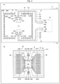
- FIG. 2 Each of (a) and (b) of Fig. 2 is a plan view illustrating a first substrate and a second substrate included in the wireless module illustrated in Fig. 1 .
- (a) of Fig. 2 is a top view (seen from above in Fig. 1 ), and (b) of Fig. 2 is a bottom view (seen from below in Fig. 1 ).
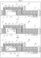
- FIG. 1 (a) through (c) of Fig. 3 are cross-sectional views illustrating the wireless module illustrated in Fig. 1 , a first modification example of the wireless module, and a second modification example of the wireless module, respectively.
- a wireless module in accordance with an aspect of the present invention is designed to transmit, or receive, or transmit and receive an RF signal in which a signal is superimposed on an electromagnetic wave belonging to a millimeter-wave band.
- a frequency of the RF signal is not limited to a particular one, provided that the frequency belongs to the millimeter-wave band.
- a frequency of 60 GHz is employed as an example.
- a wireless module 10 which is an embodiment of such a wireless module, will be described with reference to Fig. 1 , Fig. 2 , and (a) of Fig. 3 . Furthermore, a wireless module 10A, which is a first modification example of the wireless module 10, will be described with reference to (b) of Fig. 3 , and a wireless module 10B, which is a second modification example of the wireless module 10, will be described with reference to (c) of Fig. 3 .
- Fig. 1 is a perspective view illustrating the wireless module 10.
- Each of (a) and (b) of Fig. 2 is a plan view illustrating a first substrate 11 and a second substrate 21 included in the wireless module 10.
- (a) of Fig. 2 is a top view (seen from above in Fig. 1 )
- (b) of Fig. 2 is a bottom view (seen from below in Fig. 1 ).
- (a) through (c) of Fig. 3 are cross-sectional views which are taken along the line A-A' in Fig. 1 and illustrate the wireless module 10, the wireless module 10A, and the wireless module 10B, respectively.
- the line A-A' is based on a straight line passing through a baseband IC 16 and an RFIC 28, and is defined so that a part of the line A-A' passes through an outside of a through-hole 17 along a first signal line 124 illustrated in (a) of Fig. 2 .
- the wireless module 10 includes a first substrate 11, a second substrate 21, a post wall 13, a baseband IC 16, and an RFIC 28.
- the first substrate 11 is a multilayer substrate configured by stacking and bonding a plurality of substrates, each of which is made of a dielectric substance. A specific stacking structure of the first substrate 11 will be described later with reference to Fig. 3 .
- One main surface of the first substrate 11 (the main surface on the upper side in Fig. 1 ) is referred to as "main surface 111", and the other main surface of the first substrate 11 (the main surface on the lower side in Fig. 1 ) is referred to as "main surface 112".
- a region that encompasses the RFIC 28, an antenna element group 26, and a second signal line group (not illustrated in Fig. 1 ) is referred to as "second signal line region".
- the first substrate 11 has a through-hole 17 which is provided in a region facing the second signal line region.
- the post wall 13 is provided in the first substrate 11 along a whole of a side wall of the through-hole 17 so as to surround the through-hole 17.
- the post wall 13 is configured by arranging a plurality of conductor posts at predetermined intervals so as to constitute a fence-like structure.
- the second substrate 21 is a multilayer substrate configured by stacking and bonding a plurality of substrates, each of which is made of a dielectric substance. A specific stacking structure of the second substrate 21 will be described later with reference to Fig. 3 .
- the second substrate 21 is mounted so as to face the main surface 111 of the first substrate 11.
- One main surface (i.e., a main surface on the lower side in Fig. 1 ) of the second substrate 21 on a first substrate 11 side is referred to as "main surface 211"
- the other main surface (i.e., a main surface on the upper side in Fig. 1 ) of the second substrate 21 on a side opposite to the first substrate 11 is referred to as "main surface 212".
- the main surface 112 of the first substrate 11 is provided with the baseband IC 16 which processes a baseband signal.
- the main surface 211 of the second substrate 21 is provided with the RFIC 28 which processes an RF signal.
- a first signal line group 12 is provided in an inner layer of the first substrate 11.
- the first signal line group 12 is provided for transmission of the baseband signal between the baseband IC 16 and the RFIC 28, specifically, for transmission of the baseband signal in the first substrate 11.
- a second signal line group 22 is provided on the main surface 211 of the second substrate 21.
- the second signal line group 22 is provided for transmission of the RF signal between the RFIC 28 and the antenna element group 26.
- a third signal line group 25 is provided in an inner layer of the second substrate 21.
- the third signal line group 25 is provided for transmission of the baseband signal between the baseband IC 16 and the RFIC 28, specifically, for transmission of the baseband signal in the second substrate 21.
- the wireless module 10 thus configured can transmit, or receive, or transmit and receive the RF signal as above described.
- the RFIC 28 obtains a baseband signal processed by the baseband IC 16, and the RFIC 28 carries out a process of converting the baseband signal into an RF signal. The RF signal is then emitted from the antenna element group 26.
- the RFIC 28 obtains the RF signal which has been received through the antenna element group 26. Further, the RFIC 28 carries out a process of converting the RF signal into a baseband signal. The baseband signal is then supplied to the baseband IC 16.
- the wireless module 10 can be configured so as to be capable of carrying out both the transmission process and the reception process which are described above.
- the first substrate 11 in a plan view, has a rectangular shape composed of a pair of longer sides and a pair of shorter sides.
- the baseband IC 16 is mounted on a side near to one shorter side (the right shorter side in (a) of Fig. 2 ).
- the second substrate 21 is mounted on a side near to the other shorter side (the left shorter side in (a) of Fig. 2 ). The second substrate 21 will be described later with reference to (b) of Fig. 2 .
- the first substrate 11 is configured by stacking and bonding five substrates, i.e., substrates 11a through 11e.
- Each of the substrates 11a through 11e is made of a dielectric substance.
- the first substrate 11 includes a pair of outer layers, i.e., the main surfaces 111 and 112, and four inner layers interposed between adjacent ones of the substrates 11a through 11e.
- a glass epoxy resin having a specific inductive capacity ⁇ of 4.6 is employed as the dielectric substance constituting the substrates 11a through 11e.
- the glass epoxy resin is an example of glass fiber reinforced plastic (GFRP).
- a standard name of a substrate using such a glass epoxy resin can be, for example, FR-4.
- FR4 material a plate material in conformity to FR-4 (hereinafter referred to as "FR4 material") is employed as each of the substrates 11a through 11e.
- FR4 material a plate material in conformity to FR-4
- Each of the substrates 11a through 11e has a thickness of 120 ⁇ m. Therefore, a thickness t11 of the first substrate 11 (see (a) of Fig. 3 ) is 600 ⁇ m (where a thickness of the inner layer is ignored).
- the thickness, the number of pieces, and the like of the plurality of substrates which are made of the dielectric substance and constitute the first substrate 11 are not limited to the configuration described above, and can be selected as appropriate.
- the dielectric substance constituting the substrates 11a through 11e is not limited to the glass epoxy resin described above.
- the dielectric substance constituting the substrates 11a through 11e can be appropriately selected while considering physical properties such as a specific inductive capacity and a dielectric loss tangent.
- Other examples of the dielectric substance that constitutes the substrates 11a through 11e include a liquid crystal polymer (LCP) resin, an acrylic resin, glass, and the like. Note, however, that, by employing the glass epoxy resin as the dielectric substance constituting the substrates 11a through 11e, it is possible to reduce a manufacturing cost of the first substrate 11.
- LCP liquid crystal polymer
- the main surface 112 of the first substrate 11 is provided with conductor pads 161 through 166 to which terminals of the baseband IC 16 are connected (see (a) of Fig. 2 ).
- the main surface 112 is provided with a ground layer 19 constituted by a conductor film (see (a) of Fig. 3 ).
- the terminals of the baseband IC 16 are connected to the conductor pads 161 through 166 and the ground layer 19 with use of, for example, solder balls, and the baseband IC 16 is thus mounted on the main surface 112 side of the first substrate 11.
- the inner layer of the first substrate 11 includes the first signal line group 12 arranged in a pattern as illustrated in (a) of Fig. 2 .
- the first signal line group 12 is made up of six first signal lines, i.e., first signal lines 121 through 126. One ends of the first signal lines 121 through 126 are connected to the respective conductor pads 161 through 166 through respective vias.
- the first signal line group 12 and the ground layer 19 constitute a microstrip line for transmitting a baseband signal.
- the first signal line 124 is provided in the inner layer interposed between the substrate 11d and the substrate 11e.
- Each of the first signal lines 121 through 123, 125, and 126 is provided in one of the four inner layers. Note, however, that the configuration of the first signal lines is not limited to the above described configuration. Each of the first signal lines may span two or more layers.
- the main surface 111 is provided with conductor pads 151 through 156 to which terminals of the RFIC 28 are connected.
- the conductor pads 151 through 156 are connected to the respective first signal lines 121 through 126 through respective vias.
- the first substrate 11 has the through-hole 17 which is formed in a region R' inside a region where the second substrate 21 is provided (see (a) of Fig. 2 ).
- the region R' is based on a rectangular shape whose aspect ratio is close to 1:1, and has a pattern in which portions of opposite sides (i.e., the upper side and the lower side in (a) of Fig. 2 ) in the vicinity of the center approach each other so that the region R' is narrowed in that part.
- a pattern like the alphabetic letter "H" is employed as the pattern of the region R'.
- the conductor pads 151 through 156 are provided in regions corresponding to the narrowed portions of the region R'.
- region R' is not limited to the above described pattern, provided that the pattern corresponds to the second signal line region R described with reference to (b) of Fig. 2 .
- the post wall 13 is provided in the first substrate 11 along a whole of a side wall 171 of the through-hole 17 so as to surround the through-hole 17.
- the post wall 13 is configured by arranging 66 conductor posts, i.e., conductor posts 1301 through 1366 at predetermined intervals so as to constitute a fence-like structure.
- the post wall 13 reflects an electromagnetic wave having an intended frequency (i.e., 60 GHz in the present embodiment). This is achieved by appropriately designing diameters of the respective conductor posts 1301 through 1366 and the center-to-center spacing between adjacent two conductor posts. That is, the post wall 13 is an aspect of the pseudo conductor wall.
- the post wall 13 is arranged so as to shield (i) first signal lines 121 through 126 constituting the first signal line group 12 and (ii) second signal lines 2201 through 2232 constituting the second signal line group 22 described later.
- the post wall 13 is arranged along the whole of the side wall 171 of the through-hole 17.
- the post wall 13 can be provided along at least part of the side wall 171 of the through-hole 17.
- the post wall 13 can shield the first signal line group 12 and the second signal line group 22 even in a case where the conductor posts 1301 through 1315 are omitted from the conductor posts 1301 through 1366 constituting the post wall 13.
- Such a configuration is also included in the scope of the present invention.
- ground pads 1401 through 1466 are provided at respective positions of the conductor posts 1301 through 1366 so as to encompass the respective conductor posts 1301 through 1366.
- the ground pads 1401 through 1466 are collectively referred to as "ground pad group 14".
- the ground pads 1401 through 1466 are conductive pads and are shorted to the ground layer 19 via the conductor posts 1301 through 1366.
- a ground pattern 23 (described later) of the second substrate 21 illustrated in (b) of Fig. 2 and (a) of Fig. 3 is connected by using, for example, solder balls.
- the second substrate 21 has a rectangular shape composed of a pair of longer sides and a pair of shorter sides. Note, however, that the aspect ratio is closer to 1:1 as compared with the first substrate 11, that is, the second substrate 21 has a rectangular shape close to a square shape.
- a pair of opposite sides extending along the left-right direction is a pair of longer sides
- a pair of opposite sides extending along the up-down direction is a pair of shorter sides.
- a length of the pair of shorter sides of the second substrate 21 is shorter than (specifically, approximately 80 percent of) that of the pair of shorter sides of the first substrate 11.
- a length of the pair of longer sides of the second substrate 21 is shorter than (specifically, approximately half of) that of the pair of longer sides of the first substrate 11.
- the second substrate 21 is configured by stacking and bonding three substrates, i.e., substrates 21a through 21c.
- Each of the substrates 21a through 21c is made of a dielectric substance.
- the second substrate 21 includes a pair of outer layers, i.e., the main surfaces 211 and 212, and two inner layers interposed between adjacent ones of the substrates 21a through 21c.
- a liquid crystal polymer (LCP) resin is employed as the dielectric substance constituting the substrates 21a through 21c.
- LCP liquid crystal polymer
- the thickness, the number of pieces, and the like of the plurality of substrates which are made of the dielectric substance and constitute the second substrate 21 are not limited to the configuration described above, and can be selected as appropriate.
- the dielectric substance constituting the substrates 21a through 21c is not limited to the LCP resin described above.
- the dielectric substance constituting the substrates 21a through 21c can be appropriately selected while considering physical properties such as a specific inductive capacity and a dielectric loss tangent.
- Other examples of the dielectric substance that constitutes the substrates 21a through 21c include a glass fiber reinforced plastic (GFRP) resin, an acrylic resin, glass, and the like.
- GFRP resin includes a glass epoxy resin, and a standard name of a substrate using such a glass epoxy resin can be, for example, FR-4. Note, however, that, by employing the LCP resin as the dielectric substance constituting the substrates 21a through 21c, it is possible to reduce a transmission loss of an RF signal in the second signal line group 22 (described later).
- a center region of the main surface 211 of the second substrate 21 is provided with a conductor pad group 27 consisted by a plurality of conductor pads.
- the plurality of conductor pads are arranged in a lattice pattern.
- To the plurality of conductor pads one ends of the plurality of second signal lines constituting the second signal line group 22 (described later), one ends of the plurality of third signal lines constituting the third signal line group 25 (described later), and a ground layer 29 illustrated in (a) of Fig. 3 are connected.
- the terminals of the RFIC 28 are connected to the plurality of conductor pads with use of, for example, solder balls, and the RFIC 28 is thus mounted on the main surface 211 side of the second substrate 21.
- the second signal line group 22 is provided in a pattern as illustrated in (b) of Fig. 2 .
- the second signal line group 22 is made up of 32 second signal lines, i.e., second signal lines 2201 through 2232. One ends of the second signal lines 2201 through 2232 are connected to the respective plurality of conductor pads described above. Note that, in (b) of Fig. 2 , only the reference numerals 2201, 2216, 2217, and 2232 are indicated among the second signal lines 2201 through 2232, and the other reference numerals of the second signal lines are omitted.
- region R a region encompassing the second signal line group 22 and the plurality of conductor pads described above is referred to as "region R", and a ground pattern 23 surrounding the region R is provided on the outer side of the region R.
- the region R in the second substrate 21 and the region R' in the first substrate 11 face each other.
- the ground pattern 23 is provided in a region encompassing the post wall 13 and the ground pad group 14.
- the ground pattern 23 is connected to the ground pads 1401 through 1466 constituting the ground pad group 14 via, for example, solder balls.
- the third signal line group 25 (described later) and the ground pattern 23 constitute a microstrip line for transmitting a baseband signal.
- the main surface 211 is provided with conductor pads 241 through 246 to which the conductor pads 151 through 156 provided on the main surface 111 are connected.
- the conductor pads 241 through 246 are connected to the conductor pads 151 through 156 via solder balls, respectively.
- the ground pattern 23 is connected to the ground pad group 14, and the conductor pads 241 through 246 are connected to the conductor pads 151 through 156, respectively.
- the second substrate 21 is mounted on the main surface 111 side of the first substrate 11.
- the inner layer of the second substrate 21 includes the third signal line group 25 arranged in a pattern as illustrated in (b) of Fig. 2 .
- the third signal line group 25 is made up of six third signal lines. In (b) of Fig. 2 , reference numerals are not given to the six third signal lines.
- One ends of the six third signal lines are connected, through vias, to any ones of the plurality of conductor pads provided in a region in which the RFIC 28 is mounted.
- the other ends of the six third signal lines are connected to the respective conductor pads 241 through 246 through respective vias.
- Baseband signals obtained from the first signal line group 12 are supplied to the RFIC 28 through the third signal line group 25.
- the third signal line group 25 is provided in an inner layer interposed between the substrate 21a and the substrate 21b. Note, however, that the position at which the third signal line group 25 is provided is not limited to the inner layer interposed between the substrate 21a and the substrate 21b.
- the third signal line group 25 can be provided in an inner layer interposed between the substrate 21b and the substrate 21c.
- the ground layer 29 is provided in the inner layer interposed between the substrate 21a and the substrate 21b among the inner layers in the second substrate 21 (see (a) of Fig. 3 ).
- the second signal line group 22 and the ground layer 29 constitute a microstrip line for transmitting an RF signal.
- the inner layer of the second substrate 21 includes the antenna element group 26 arranged in a pattern as illustrated in (b) of Fig. 2 .
- the antenna element group 26 is constituted by two sets of 64 antenna elements arranged in a matrix of 16 rows and 4 columns.
- the ground layer 29 is provided with a coupling window group 291 constituted by 128 coupling windows.
- the coupling windows are provided in respective regions corresponding to centers of the respective 128 antenna elements constituting the antenna element group 26 in a plan view of the ground layer 29.
- (a) of Fig. 3 illustrates four coupling windows of the coupling windows constituting the coupling window group 291.
- the second signal lines 2201 through 2232 are electromagnetically coupled to the respective 128 antenna elements constituting the antenna element group 26 via the respective 128 coupling windows provided in the ground layer 29.
- the 128 coupling windows correspond to the 128 antenna elements, respectively.
- the 128 coupling windows are provided in respective regions in which the second signal lines 2201 through 2232 are overlapped on the respective 128 antenna elements constituting the antenna element group 26.
- the antenna element group 26 is provided in an inner layer interposed between the substrate 21b and the substrate 21c. Note, however, that the position at which the antenna element group 26 is provided is not limited to the inner layer interposed between the substrate 21b and the substrate 21c.
- the antenna element group 26 can be provided on the main surface 212 of the second substrate 21.
- wireless module 10A which is a first modification example of the wireless module 10, with reference to (b) of Fig. 3 .
- the wireless module 10A is obtained by replacing the post wall 13 provided in the wireless module 10 with a conductor wall 13A. That is, a configuration of the wireless module 10A other than the conductor wall 13A is the same as that of the wireless module 10. Therefore, in the present modification example, only the conductor wall 13A will be described, and descriptions of other configurations will be omitted.
- the conductor wall 13A is a conductor film provided in the side wall 171 of the through-hole 17.
- the conductor wall 13A is provided along a whole of the side wall 171 of the through-hole 17. Note, however, that the conductor wall 13A can be provided along a part of the side wall 171 of the through-hole 17. This point is the same as the post wall 13.
- the conductor wall 13A thus configured shields the first signal lines 121 through 126 and the second signal lines 2201 through 2232.
- both of the post wall 13 and the conductor wall 13A can be provided.
- the wireless module 10B is obtained by replacing the first substrate 11 provided in the wireless module 10 with a first substrate 11B. That is, a configuration of the wireless module 10B other than the first substrate 11B is the same as that of the wireless module 10. Therefore, in the present modification example, only the first substrate 11B will be described, and descriptions of other configurations will be omitted.
- the first substrate 11B is configured by stacking and bonding five substrates, i.e., substrates 11a, 11b, 11c, 11d, and 11Be.
- the substrates 11a through 11d included in the first substrate 11B are the same as the substrates 11a through 11d included in the first substrate 11.
- the through-hole which is provided in the region R' of the substrate 11e included in the first substrate 11, is omitted.
- a non-through-hole 17B is provided in place of the through-hole 17.
- a depth d17B of the non-through-hole 17B is 480 ⁇ m.
- the conductor wall 13A instead of the post wall 13, and it is also possible to employ both of the post wall 13 and the conductor wall 13A.
- the conductor wall 13A can be provided on at least part of a main surface of the substrate 11Be on a substrate 11d side, as well as on at least part of a side wall of the non-through-hole 17B.
- each of the wireless modules 10, 10A, and 10B includes the RFIC 28, the baseband IC 16, the first substrate 11, the first signal line group 12, and one or more antenna elements.
- the first substrate 11 is provided with at least one of the conductor wall 13A and the post wall 13 which is a pseudo conductor wall.
- the RFIC 28 processes an RF signal, which is a millimeter-wave signal.
- the baseband IC 16 processes a baseband signal.
- the one or more antenna elements are the antenna element group 26, which is constituted by the plurality of antenna elements in the embodiment described above.
- the antenna element group 26 is provided in at least any of the inner layer of the second substrate 21 and the main surface 212, and is supplied with electric power through the second signal lines 2201 through 2232.
- the baseband IC 16 is mounted on at least one main surface (i.e., the main surface 112 in the embodiment described above) of the first substrate 11.
- the first substrate 11 is provided with the first signal lines 121 through 126 for transmitting the baseband signal.
- the second substrate 21 is mounted on the main surface 111 side of the first substrate 11.
- the main surface 211 which is the main surface of the second substrate on the main surface 111 side, is provided with the RFIC 28.
- the main surface 211 is provided with the second signal lines 2201 through 2232 for transmitting the RF signal, which is a millimeter-wave signal to be processed by the RFIC 28.
- the conductor wall 13A is constituted by a conductor film.
- the post wall 13 is configured by arranging the conductor posts 1301 through 1366 so as to constitute a fence-like structure.
- the conductor wall 13A and the post wall 13 are arranged so as to shield the first signal lines 121 through 126 and the second signal lines 2201 through 2232.
- the region encompassing the second signal lines 2201 through 2232 is referred to as the second signal line region R.
- the region of the main surface 111 of the first substrate 11, which region faces the second signal line region R, is provided with the through-hole 17 or the non-through-hole 17B corresponding to the second signal line region R.
- the surface of the second signal line group 22 on the first substrate 11 side is to be in contact with the air, and this makes it possible to reduce a transmission loss (dielectric loss).
- the RFIC 28 is accommodated in the through-hole 17 or the non-through-hole 17B, and this makes it possible to achieve downsizing (or profile reduction) of the wireless module.
- At least one of the conductor wall 13A and the post wall 13 is preferably provided along at least part of the side wall of the through-hole 17 or of the non-through-hole 17B.
- At least one of the conductor wall 13A and the post wall 13 is provided along the whole of the side wall of the through-hole 17 or of the non-through-hole 17B.
- a thickness t11 of the first substrate 11 is preferably equal to or greater than a quarter wavelength of an effective wavelength of the RF signal in the air.
- a frequency of the RF signal is 60 GHz.
- the quarter wavelength of the effective wavelength of the RF signal in the air is 1.25 mm. Therefore, in the present embodiment, the thickness t11 is preferably 1.25 mm or more.
- each of the thickness t11 and the depth d17B of the non-through-hole 17B is preferably equal to or greater than the above quarter wavelength.
- the RFIC 28 is provided in the second signal line region R of the second substrate 21.
- the baseband IC 16 which (i) is mounted on at least one of the main surface 111 and the main surface 112 of the first substrate 11 and (ii) supplies a baseband signal to the first signal lines 121 through 126 and/or is supplied with a baseband signal through the first signal lines 121 through 126.
- the conductor wall 13A and the post wall 13 are shorted to the ground layer 19 which constitutes the signal line path (i.e., the microstrip line in the present embodiment) together with the first signal lines 121 through 126.
- the signal line path i.e., the microstrip line in the present embodiment
- the first signal lines 121 through 126 and the second signal lines 2201 through 2232 are employed.
- each of the wireless modules 10, 10A, and 10B can include a single first signal line and a single second signal line.
- the antenna element group 26 constituted by the plurality of antenna elements is employed. Note, however, that each of the wireless modules 10, 10A, and 10B can include a single antenna element.
- microstrip lines are employed as the signal line path including the first signal line group 12, the signal line path including the second signal line group 22, and the signal line path including the third signal line group 25, respectively.
- the signal line path including the first signal line group 12, the signal line path including the second signal line group 22, and the signal line path including the third signal line group 25 can be coplanar lines, respectively.
- a wireless module in accordance with a first aspect of the present invention employs a configuration including: an RFIC which processes an RF signal; a baseband IC which processes a baseband signal; a first substrate which is provided with the baseband IC on at least one main surface, the first substrate being provided with one or more first signal lines for transmitting the baseband signal; a second substrate which is mounted on one main surface side of the first substrate, the RFIC being mounted on a main surface of the second substrate on a first substrate side, and one or more second signal lines for transmitting the RF signal being provided on the main surface on the first substrate side; and one or more antenna elements which are provided on the second substrate and are supplied with electric power through the one or more second signal lines, in which the first substrate is provided with at least one of a conductor wall and a pseudo conductor wall for shielding the one or more first signal lines and the one or more second signal lines.
- At least one of the conductor wall and the pseudo conductor wall is provided in the first substrate so as to shield the one or more first signal lines and the one or more second signal lines, and this makes it possible to reduce an electromagnetic coupling that can occur between the first signal line and the second signal line.
- the wireless module in accordance with a second aspect of the present invention includes, in addition to the configuration of the wireless module in accordance with the above described first aspect, a configuration in which: the main surface of the second substrate on the first substrate side has a second signal line region which encompasses the one or more second signal lines; a through-hole or non-through-hole corresponding to the second signal line region being provided in a region of the one main surface of the first substrate, the region facing the second signal line region; and at least one of the conductor wall and the pseudo conductor wall is provided along at least part of a side wall of the through-hole or non-through-hole.
- the through-hole or non-through-hole corresponding to the second signal line region is provided in the region which is of the one main surface of the first substrate and faces the second signal line region, the surface of the one or more second signal lines on the first substrate side is to be in contact with the air, and this makes it possible to reduce a transmission loss (dielectric loss).
- the RFIC is accommodated in the through-hole or non-through-hole, and this makes it possible to achieve downsizing (or profile reduction) of the wireless module.
- the wireless module in accordance with a third aspect of the present invention includes, in addition to the configuration of the wireless module in accordance with the above described second aspect, a configuration in which: at least one of the conductor wall and the pseudo conductor wall is provided along a whole of the side wall of the through-hole or non-through-hole.
- the through-hole or non-through-hole corresponding to the second signal line region is provided in the region which is of the one main surface of the first substrate and faces the second signal line region, it is possible to surely reduce an electromagnetic coupling that can occur between the first signal line and the second signal line.
- the wireless module in accordance with a fourth aspect of the present invention includes, in addition to the configuration of the wireless module in accordance with the above described second or third aspect, a configuration in which: in a case where the through-hole or non-through-hole is a through-hole, a thickness of the first substrate is equal to or greater than a quarter wavelength of an effective wavelength of the RF signal in air; and in a case where the through-hole or non-through-hole is a non-through-hole, a depth of the non-through-hole is equal to or greater than the quarter wavelength.
- the wireless module in accordance with a fifth aspect of the present invention includes, in addition to the configuration of the wireless module in accordance with any one of the above described second through fourth aspects, a configuration in which: the RFIC is provided in the second signal line region of the second substrate.
- the RFIC is accommodated in the through-hole or non-through-hole, and this makes it possible to achieve downsizing (or profile reduction) of the wireless module.
- the wireless module in accordance with a sixth aspect of the present invention includes, in addition to the configuration of the wireless module in accordance with any one of the above described first through fifth aspects, a configuration in which: at least one of the conductor wall and the pseudo conductor wall is shorted to a ground layer that constitutes a signal line path together with the one or more first signal lines.
- the wireless module thus configured, it is possible to more surely reduce an electromagnetic coupling that can occur between the first signal line and the second signal line.
- the present invention is not limited to the embodiment and modification examples described above, but can be altered by a skilled person in the art within the scope of the claims.
- the present invention also encompasses in its technical scope any embodiment based on an appropriate combination of the technical means disclosed in different embodiment and modification examples.
Landscapes
- Engineering & Computer Science (AREA)
- Microelectronics & Electronic Packaging (AREA)
- Transceivers (AREA)
- Waveguides (AREA)
- Variable-Direction Aerials And Aerial Arrays (AREA)
Abstract
Description
- The present invention relates to a wireless module which can be used in a millimeter-wave band.
-
Fig. 1 ofPatent Literature 1 shows a high-frequency multichip module which includes two ceramic substrates and a multilayer glass epoxy substrate. Each of the ceramic substrates is provided with two bare chip ICs on one surface thereof. The multilayer glass epoxy substrate has a plurality of metal layers and two through holes. The two ceramic substrates are mounted on one surface of the multilayer glass epoxy substrate such that the two bare chip ICs mounted on each of the two ceramic substrates face the corresponding through-hole. In other words, the two ceramic substrates are mounted on one surface of the multilayer glass epoxy substrate such that, in a plan view, the two bare chip ICs are encompassed by the corresponding one of the two through holes. - Note that the bare chip IC, the ceramic substrate, the multilayer glass epoxy substrate, and the high-frequency multichip module are read as an RFIC, a second substrate, a first substrate, and the wireless module in accordance with an aspect of the present invention, respectively. Moreover, the through hole is read as a through-hole or a non-through-hole in accordance with an aspect of the present invention. In addition, a part of the plurality of metal layers is read as one or more first signal lines in accordance with an aspect of the present invention. In the following descriptions, the names of members of the invention disclosed in
Fig. 1 ofPatent Literature 1 are read as the name of members in an aspect of the present invention. - [Patent Literature 1]
Japanese Patent Application Publication Tokukaihei No. 2002-222912 - The wireless module as described above may be configured as follows. That is, a baseband IC that processes a baseband signal is mounted on one main surface of a first substrate. Further, a second substrate is provided with a second signal line for transmitting an RF signal, which is a millimeter-wave signal supplied from an RFIC, and with an antenna element supplied with electric power through the second signal line. In this configuration, the baseband signal processed by the baseband IC is transmitted through the first signal line. The wireless module thus configured can transmit, or receive, or transmit and receive the RF signal.
- In order to reduce a transmission loss in such a wireless module, it is preferable that the second signal line is not provided in an inner layer of the second substrate but is provided on one of two main surfaces of the second substrate. More preferably, the second signal line is provided on a main surface of the second substrate on a first substrate side. This is because the RF signal emitted from the antenna element is radiated to the space through another main surface of the second substrate, said another main surface not facing the first substrate.
- In the wireless module having the more preferable configuration, the second signal line is provided on the main surface of the second substrate on the first substrate side, and this can result in an electromagnetic coupling between the first signal line and the second signal line. This can further cause interference between the baseband signal and the RF signal and, due to this, there is a possibility that at least one of the baseband signal and the RF signal is deteriorated.
- An aspect of the present invention is accomplished in view of the above described problems, and its object is to reduce an electromagnetic coupling that can occur between the first signal line and the second signal line in the wireless module including (i) the first substrate provided with the first signal line and (ii) the second substrate which is mounted on a first main surface of the first substrate and is provided with the second signal line on a main surface on the first main surface side.
- In order to solve the problems, a wireless module in accordance with a first aspect of the present invention employs a configuration including: an RFIC which processes an RF signal; a baseband IC which processes a baseband signal; a first substrate which is provided with the baseband IC on at least one main surface, the first substrate being provided with one or more first signal lines for transmitting the baseband signal; a second substrate which is mounted on one main surface side of the first substrate, the RFIC being mounted on a main surface of the second substrate on a first substrate side, and one or more second signal lines for transmitting the RF signal being provided on the main surface on the first substrate side; and one or more antenna elements which are provided on the second substrate and are supplied with electric power through the one or more second signal lines, in which the first substrate is provided with at least one of a conductor wall and a pseudo conductor wall for shielding the one or more first signal lines and the one or more second signal lines.
- According to an aspect of the present invention, it is possible to reduce an electromagnetic coupling that can occur between the first signal line and the second signal line in the wireless module including (i) the first substrate provided with the first signal line and (ii) the second substrate which is mounted on a first main surface of the first substrate and is provided with the second signal line on a main surface on the first main surface side.
-
Fig. 1 is a perspective view illustrating a wireless module in accordance with an embodiment of the present invention. - Each of (a) and (b) of
Fig. 2 is a plan view illustrating a first substrate and a second substrate included in the wireless module illustrated inFig. 1 .(a) ofFig. 2 is a top view (seen from above inFig. 1 ), and (b) ofFig. 2 is a bottom view (seen from below inFig. 1 ). - (a) through (c) of
Fig. 3 are cross-sectional views illustrating the wireless module illustrated inFig. 1 , a first modification example of the wireless module, and a second modification example of the wireless module, respectively. - A wireless module in accordance with an aspect of the present invention is designed to transmit, or receive, or transmit and receive an RF signal in which a signal is superimposed on an electromagnetic wave belonging to a millimeter-wave band. A frequency of the RF signal is not limited to a particular one, provided that the frequency belongs to the millimeter-wave band. Hereinafter, a frequency of 60 GHz is employed as an example.
- A
wireless module 10, which is an embodiment of such a wireless module, will be described with reference toFig. 1 ,Fig. 2 , and(a) ofFig. 3 . Furthermore, awireless module 10A, which is a first modification example of thewireless module 10, will be described with reference to (b) ofFig. 3 , and awireless module 10B, which is a second modification example of thewireless module 10, will be described with reference to (c) ofFig. 3 . -
Fig. 1 is a perspective view illustrating thewireless module 10. Each of (a) and (b) ofFig. 2 is a plan view illustrating afirst substrate 11 and asecond substrate 21 included in thewireless module 10. (a) ofFig. 2 is a top view (seen from above inFig. 1 ), and (b) ofFig. 2 is a bottom view (seen from below inFig. 1 ). (a) through (c) ofFig. 3 are cross-sectional views which are taken along the line A-A' inFig. 1 and illustrate thewireless module 10, thewireless module 10A, and thewireless module 10B, respectively. Note that the line A-A' is based on a straight line passing through abaseband IC 16 and anRFIC 28, and is defined so that a part of the line A-A' passes through an outside of a through-hole 17 along afirst signal line 124 illustrated in (a) ofFig. 2 . - As illustrated in
Fig. 1 , thewireless module 10 includes afirst substrate 11, asecond substrate 21, apost wall 13, abaseband IC 16, and anRFIC 28. - The
first substrate 11 is a multilayer substrate configured by stacking and bonding a plurality of substrates, each of which is made of a dielectric substance. A specific stacking structure of thefirst substrate 11 will be described later with reference toFig. 3 . One main surface of the first substrate 11 (the main surface on the upper side inFig. 1 ) is referred to as "main surface 111", and the other main surface of the first substrate 11 (the main surface on the lower side inFig. 1 ) is referred to as "main surface 112". - In a plan view of the
main surface 111, a region that encompasses theRFIC 28, anantenna element group 26, and a second signal line group (not illustrated inFig. 1 ) is referred to as "second signal line region". Thefirst substrate 11 has a through-hole 17 which is provided in a region facing the second signal line region. These arrangements will be described later with reference toFig. 2 . - The
post wall 13 is provided in thefirst substrate 11 along a whole of a side wall of the through-hole 17 so as to surround the through-hole 17. Thepost wall 13 is configured by arranging a plurality of conductor posts at predetermined intervals so as to constitute a fence-like structure. - The
second substrate 21 is a multilayer substrate configured by stacking and bonding a plurality of substrates, each of which is made of a dielectric substance. A specific stacking structure of thesecond substrate 21 will be described later with reference toFig. 3 . Thesecond substrate 21 is mounted so as to face themain surface 111 of thefirst substrate 11. One main surface (i.e., a main surface on the lower side inFig. 1 ) of thesecond substrate 21 on afirst substrate 11 side is referred to as "main surface 211", and the other main surface (i.e., a main surface on the upper side inFig. 1 ) of thesecond substrate 21 on a side opposite to thefirst substrate 11 is referred to as "main surface 212". - The
main surface 112 of thefirst substrate 11 is provided with thebaseband IC 16 which processes a baseband signal. Moreover, themain surface 211 of thesecond substrate 21 is provided with theRFIC 28 which processes an RF signal. - A first
signal line group 12 is provided in an inner layer of thefirst substrate 11. The firstsignal line group 12 is provided for transmission of the baseband signal between thebaseband IC 16 and theRFIC 28, specifically, for transmission of the baseband signal in thefirst substrate 11. A secondsignal line group 22 is provided on themain surface 211 of thesecond substrate 21. The secondsignal line group 22 is provided for transmission of the RF signal between theRFIC 28 and theantenna element group 26. A thirdsignal line group 25 is provided in an inner layer of thesecond substrate 21. The thirdsignal line group 25 is provided for transmission of the baseband signal between thebaseband IC 16 and theRFIC 28, specifically, for transmission of the baseband signal in thesecond substrate 21. These arrangements will be described later with reference toFig. 2 . - The
wireless module 10 thus configured can transmit, or receive, or transmit and receive the RF signal as above described. - In a case where the
wireless module 10 transmits an RF signal, theRFIC 28 obtains a baseband signal processed by thebaseband IC 16, and theRFIC 28 carries out a process of converting the baseband signal into an RF signal. The RF signal is then emitted from theantenna element group 26. - In a case where the
wireless module 10 receives an RF signal, theRFIC 28 obtains the RF signal which has been received through theantenna element group 26. Further, theRFIC 28 carries out a process of converting the RF signal into a baseband signal. The baseband signal is then supplied to thebaseband IC 16. - Note that, in a case where the
wireless module 10 transmits and receives an RF signal, thewireless module 10 can be configured so as to be capable of carrying out both the transmission process and the reception process which are described above. - As illustrated in (a) of
Fig. 2 , thefirst substrate 11, in a plan view, has a rectangular shape composed of a pair of longer sides and a pair of shorter sides. In thefirst substrate 11, thebaseband IC 16 is mounted on a side near to one shorter side (the right shorter side in (a) ofFig. 2 ). Further, thesecond substrate 21 is mounted on a side near to the other shorter side (the left shorter side in (a) ofFig. 2 ). Thesecond substrate 21 will be described later with reference to (b) ofFig. 2 . - As illustrated in (a) of
Fig. 3 , i.e., in the cross-sectional view, thefirst substrate 11 is configured by stacking and bonding five substrates, i.e.,substrates 11a through 11e. Each of thesubstrates 11a through 11e is made of a dielectric substance. As such, thefirst substrate 11 includes a pair of outer layers, i.e., themain surfaces substrates 11a through 11e. - In the present embodiment, a glass epoxy resin having a specific inductive capacity ε of 4.6 is employed as the dielectric substance constituting the
substrates 11a through 11e. The glass epoxy resin is an example of glass fiber reinforced plastic (GFRP). A standard name of a substrate using such a glass epoxy resin can be, for example, FR-4. In other words, in the present embodiment, a plate material in conformity to FR-4 (hereinafter referred to as "FR4 material") is employed as each of thesubstrates 11a through 11e. Each of thesubstrates 11a through 11e has a thickness of 120 µm. Therefore, a thickness t11 of the first substrate 11 (see (a) ofFig. 3 ) is 600 µm (where a thickness of the inner layer is ignored). - Note, however, that the thickness, the number of pieces, and the like of the plurality of substrates which are made of the dielectric substance and constitute the
first substrate 11 are not limited to the configuration described above, and can be selected as appropriate. - The dielectric substance constituting the
substrates 11a through 11e is not limited to the glass epoxy resin described above. The dielectric substance constituting thesubstrates 11a through 11e can be appropriately selected while considering physical properties such as a specific inductive capacity and a dielectric loss tangent. Other examples of the dielectric substance that constitutes thesubstrates 11a through 11e include a liquid crystal polymer (LCP) resin, an acrylic resin, glass, and the like. Note, however, that, by employing the glass epoxy resin as the dielectric substance constituting thesubstrates 11a through 11e, it is possible to reduce a manufacturing cost of thefirst substrate 11. - The
main surface 112 of thefirst substrate 11 is provided withconductor pads 161 through 166 to which terminals of thebaseband IC 16 are connected (see (a) ofFig. 2 ). Themain surface 112 is provided with aground layer 19 constituted by a conductor film (see (a) ofFig. 3 ). The terminals of thebaseband IC 16 are connected to theconductor pads 161 through 166 and theground layer 19 with use of, for example, solder balls, and thebaseband IC 16 is thus mounted on themain surface 112 side of thefirst substrate 11. - The inner layer of the
first substrate 11 includes the firstsignal line group 12 arranged in a pattern as illustrated in (a) ofFig. 2 . The firstsignal line group 12 is made up of six first signal lines, i.e.,first signal lines 121 through 126. One ends of thefirst signal lines 121 through 126 are connected to therespective conductor pads 161 through 166 through respective vias. The firstsignal line group 12 and theground layer 19 constitute a microstrip line for transmitting a baseband signal. - As illustrated in (a) of
Fig. 3 , thefirst signal line 124 is provided in the inner layer interposed between thesubstrate 11d and thesubstrate 11e. Each of thefirst signal lines 121 through 123, 125, and 126 is provided in one of the four inner layers. Note, however, that the configuration of the first signal lines is not limited to the above described configuration. Each of the first signal lines may span two or more layers. - As illustrated in (a) of
Fig. 2 , themain surface 111 is provided withconductor pads 151 through 156 to which terminals of theRFIC 28 are connected. Theconductor pads 151 through 156 are connected to the respectivefirst signal lines 121 through 126 through respective vias. - In the plan view, the
first substrate 11 has the through-hole 17 which is formed in a region R' inside a region where thesecond substrate 21 is provided (see (a) ofFig. 2 ). The region R' is based on a rectangular shape whose aspect ratio is close to 1:1, and has a pattern in which portions of opposite sides (i.e., the upper side and the lower side in (a) ofFig. 2 ) in the vicinity of the center approach each other so that the region R' is narrowed in that part. In the present embodiment, a pattern like the alphabetic letter "H" is employed as the pattern of the region R'. Note that theconductor pads 151 through 156 are provided in regions corresponding to the narrowed portions of the region R'. - Note, however, that the region R' is not limited to the above described pattern, provided that the pattern corresponds to the second signal line region R described with reference to (b) of
Fig. 2 . - The
post wall 13 is provided in thefirst substrate 11 along a whole of aside wall 171 of the through-hole 17 so as to surround the through-hole 17. Thepost wall 13 is configured by arranging 66 conductor posts, i.e.,conductor posts 1301 through 1366 at predetermined intervals so as to constitute a fence-like structure. Thepost wall 13 reflects an electromagnetic wave having an intended frequency (i.e., 60 GHz in the present embodiment). This is achieved by appropriately designing diameters of therespective conductor posts 1301 through 1366 and the center-to-center spacing between adjacent two conductor posts. That is, thepost wall 13 is an aspect of the pseudo conductor wall. - The
post wall 13 is arranged so as to shield (i)first signal lines 121 through 126 constituting the firstsignal line group 12 and (ii)second signal lines 2201 through 2232 constituting the secondsignal line group 22 described later. In the present embodiment, thepost wall 13 is arranged along the whole of theside wall 171 of the through-hole 17. - Note, however, that the
post wall 13 can be provided along at least part of theside wall 171 of the through-hole 17. For example, thepost wall 13 can shield the firstsignal line group 12 and the secondsignal line group 22 even in a case where the conductor posts 1301 through 1315 are omitted from the conductor posts 1301 through 1366 constituting thepost wall 13. Such a configuration is also included in the scope of the present invention. - In the
main surface 111,ground pads 1401 through 1466 are provided at respective positions of the conductor posts 1301 through 1366 so as to encompass therespective conductor posts 1301 through 1366. Theground pads 1401 through 1466 are collectively referred to as "ground pad group 14". Theground pads 1401 through 1466 are conductive pads and are shorted to theground layer 19 via the conductor posts 1301 through 1366. To theground pads 1401 through 1466, a ground pattern 23 (described later) of thesecond substrate 21 illustrated in (b) ofFig. 2 and(a) ofFig. 3 is connected by using, for example, solder balls. - As illustrated in (b) of
Fig. 2 , in the plan view, thesecond substrate 21 has a rectangular shape composed of a pair of longer sides and a pair of shorter sides. Note, however, that the aspect ratio is closer to 1:1 as compared with thefirst substrate 11, that is, thesecond substrate 21 has a rectangular shape close to a square shape. In thesecond substrate 21 illustrated in (b) ofFig. 2 , a pair of opposite sides extending along the left-right direction is a pair of longer sides, and a pair of opposite sides extending along the up-down direction is a pair of shorter sides. A length of the pair of shorter sides of thesecond substrate 21 is shorter than (specifically, approximately 80 percent of) that of the pair of shorter sides of thefirst substrate 11. A length of the pair of longer sides of thesecond substrate 21 is shorter than (specifically, approximately half of) that of the pair of longer sides of thefirst substrate 11. - As illustrated in (a) of
Fig. 3 , i.e., in the cross-sectional view, thesecond substrate 21 is configured by stacking and bonding three substrates, i.e.,substrates 21a through 21c. Each of thesubstrates 21a through 21c is made of a dielectric substance. As such, thesecond substrate 21 includes a pair of outer layers, i.e., themain surfaces substrates 21a through 21c. - In the present embodiment, a liquid crystal polymer (LCP) resin is employed as the dielectric substance constituting the
substrates 21a through 21c. Each of thesubstrates 21a through 21c has a thickness of 50 µm to 100 µm. - Note, however, that the thickness, the number of pieces, and the like of the plurality of substrates which are made of the dielectric substance and constitute the
second substrate 21 are not limited to the configuration described above, and can be selected as appropriate. - The dielectric substance constituting the
substrates 21a through 21c is not limited to the LCP resin described above. The dielectric substance constituting thesubstrates 21a through 21c can be appropriately selected while considering physical properties such as a specific inductive capacity and a dielectric loss tangent. Other examples of the dielectric substance that constitutes thesubstrates 21a through 21c include a glass fiber reinforced plastic (GFRP) resin, an acrylic resin, glass, and the like. Further, an example of the GFRP resin includes a glass epoxy resin, and a standard name of a substrate using such a glass epoxy resin can be, for example, FR-4. Note, however, that, by employing the LCP resin as the dielectric substance constituting thesubstrates 21a through 21c, it is possible to reduce a transmission loss of an RF signal in the second signal line group 22 (described later). - As illustrated in (b) of
Fig. 2 , a center region of themain surface 211 of thesecond substrate 21 is provided with aconductor pad group 27 consisted by a plurality of conductor pads. The plurality of conductor pads are arranged in a lattice pattern. To the plurality of conductor pads, one ends of the plurality of second signal lines constituting the second signal line group 22 (described later), one ends of the plurality of third signal lines constituting the third signal line group 25 (described later), and aground layer 29 illustrated in (a) ofFig. 3 are connected. The terminals of theRFIC 28 are connected to the plurality of conductor pads with use of, for example, solder balls, and theRFIC 28 is thus mounted on themain surface 211 side of thesecond substrate 21. - On the
main surface 211, the secondsignal line group 22 is provided in a pattern as illustrated in (b) ofFig. 2 . The secondsignal line group 22 is made up of 32 second signal lines, i.e.,second signal lines 2201 through 2232. One ends of thesecond signal lines 2201 through 2232 are connected to the respective plurality of conductor pads described above. Note that, in (b) ofFig. 2 , only thereference numerals second signal lines 2201 through 2232, and the other reference numerals of the second signal lines are omitted. - In the
main surface 211, a region encompassing the secondsignal line group 22 and the plurality of conductor pads described above is referred to as "region R", and aground pattern 23 surrounding the region R is provided on the outer side of the region R. In thewireless module 10, the region R in thesecond substrate 21 and the region R' in thefirst substrate 11 face each other. In the plan view of thewireless module 10, theground pattern 23 is provided in a region encompassing thepost wall 13 and theground pad group 14. Theground pattern 23 is connected to theground pads 1401 through 1466 constituting theground pad group 14 via, for example, solder balls. The third signal line group 25 (described later) and theground pattern 23 constitute a microstrip line for transmitting a baseband signal. - As illustrated in (b) of
Fig. 2 , themain surface 211 is provided withconductor pads 241 through 246 to which theconductor pads 151 through 156 provided on themain surface 111 are connected. Theconductor pads 241 through 246 are connected to theconductor pads 151 through 156 via solder balls, respectively. - As such, the
ground pattern 23 is connected to theground pad group 14, and theconductor pads 241 through 246 are connected to theconductor pads 151 through 156, respectively. Thus, thesecond substrate 21 is mounted on themain surface 111 side of thefirst substrate 11. - The inner layer of the
second substrate 21 includes the thirdsignal line group 25 arranged in a pattern as illustrated in (b) ofFig. 2 . The thirdsignal line group 25 is made up of six third signal lines. In (b) ofFig. 2 , reference numerals are not given to the six third signal lines. One ends of the six third signal lines are connected, through vias, to any ones of the plurality of conductor pads provided in a region in which theRFIC 28 is mounted. The other ends of the six third signal lines are connected to therespective conductor pads 241 through 246 through respective vias. Baseband signals obtained from the firstsignal line group 12 are supplied to theRFIC 28 through the thirdsignal line group 25. - As illustrated in (a) of
Fig. 3 , the thirdsignal line group 25 is provided in an inner layer interposed between thesubstrate 21a and thesubstrate 21b. Note, however, that the position at which the thirdsignal line group 25 is provided is not limited to the inner layer interposed between thesubstrate 21a and thesubstrate 21b. The thirdsignal line group 25 can be provided in an inner layer interposed between thesubstrate 21b and thesubstrate 21c. - The
ground layer 29 is provided in the inner layer interposed between thesubstrate 21a and thesubstrate 21b among the inner layers in the second substrate 21 (see (a) ofFig. 3 ). The secondsignal line group 22 and theground layer 29 constitute a microstrip line for transmitting an RF signal. - The inner layer of the
second substrate 21 includes theantenna element group 26 arranged in a pattern as illustrated in (b) ofFig. 2 . Theantenna element group 26 is constituted by two sets of 64 antenna elements arranged in a matrix of 16 rows and 4 columns. - In the present embodiment, as illustrated in (b) of
Fig. 2 and(a) ofFig. 3 , four antenna elements arranged in the same row in one set of the antenna elements are supplied with electric power through one of thesecond signal lines 2201 through 2232. - The
ground layer 29 is provided with acoupling window group 291 constituted by 128 coupling windows. The coupling windows are provided in respective regions corresponding to centers of the respective 128 antenna elements constituting theantenna element group 26 in a plan view of theground layer 29. (a) ofFig. 3 illustrates four coupling windows of the coupling windows constituting thecoupling window group 291. Thesecond signal lines 2201 through 2232 are electromagnetically coupled to the respective 128 antenna elements constituting theantenna element group 26 via the respective 128 coupling windows provided in theground layer 29. Note that the 128 coupling windows correspond to the 128 antenna elements, respectively. In the plan view, the 128 coupling windows are provided in respective regions in which thesecond signal lines 2201 through 2232 are overlapped on the respective 128 antenna elements constituting theantenna element group 26. - As illustrated in (a) of
Fig. 3 , theantenna element group 26 is provided in an inner layer interposed between thesubstrate 21b and thesubstrate 21c. Note, however, that the position at which theantenna element group 26 is provided is not limited to the inner layer interposed between thesubstrate 21b and thesubstrate 21c. Theantenna element group 26 can be provided on themain surface 212 of thesecond substrate 21. - The following description will discuss a
wireless module 10A, which is a first modification example of thewireless module 10, with reference to (b) ofFig. 3 . - The
wireless module 10A is obtained by replacing thepost wall 13 provided in thewireless module 10 with aconductor wall 13A. That is, a configuration of thewireless module 10A other than theconductor wall 13A is the same as that of thewireless module 10. Therefore, in the present modification example, only theconductor wall 13A will be described, and descriptions of other configurations will be omitted. - As illustrated in (b) of
Fig. 3 , theconductor wall 13A is a conductor film provided in theside wall 171 of the through-hole 17. In this modification example, theconductor wall 13A is provided along a whole of theside wall 171 of the through-hole 17. Note, however, that theconductor wall 13A can be provided along a part of theside wall 171 of the through-hole 17. This point is the same as thepost wall 13. - The
conductor wall 13A thus configured shields thefirst signal lines 121 through 126 and thesecond signal lines 2201 through 2232. - In a modification example of the present invention, both of the
post wall 13 and theconductor wall 13A can be provided. - The following description will discuss a
wireless module 10B, which is a second modification example of thewireless module 10, with reference to (c) ofFig. 3 . - The
wireless module 10B is obtained by replacing thefirst substrate 11 provided in thewireless module 10 with afirst substrate 11B. That is, a configuration of thewireless module 10B other than thefirst substrate 11B is the same as that of thewireless module 10. Therefore, in the present modification example, only thefirst substrate 11B will be described, and descriptions of other configurations will be omitted. - As illustrated in (c) of
Fig. 3 , thefirst substrate 11B is configured by stacking and bonding five substrates, i.e.,substrates substrates 11a through 11d included in thefirst substrate 11B are the same as thesubstrates 11a through 11d included in thefirst substrate 11. Meanwhile, in the substrate 11Be, the through-hole, which is provided in the region R' of thesubstrate 11e included in thefirst substrate 11, is omitted. - Consequently, in the region R' of the
first substrate 11B, a non-through-hole 17B is provided in place of the through-hole 17. In this modification example, a depth d17B of the non-through-hole 17B is 480 µm. - Further, in the
wireless module 10B, it is possible to employ theconductor wall 13A instead of thepost wall 13, and it is also possible to employ both of thepost wall 13 and theconductor wall 13A. In a case where theconductor wall 13A is employed, theconductor wall 13A can be provided on at least part of a main surface of the substrate 11Be on asubstrate 11d side, as well as on at least part of a side wall of the non-through-hole 17B. - Aspects of the present invention can also be expressed as follows:
As described above, each of thewireless modules RFIC 28, thebaseband IC 16, thefirst substrate 11, the firstsignal line group 12, and one or more antenna elements. Thefirst substrate 11 is provided with at least one of theconductor wall 13A and thepost wall 13 which is a pseudo conductor wall. - The
RFIC 28 processes an RF signal, which is a millimeter-wave signal. Thebaseband IC 16 processes a baseband signal. The one or more antenna elements are theantenna element group 26, which is constituted by the plurality of antenna elements in the embodiment described above. Theantenna element group 26 is provided in at least any of the inner layer of thesecond substrate 21 and themain surface 212, and is supplied with electric power through thesecond signal lines 2201 through 2232. - The
baseband IC 16 is mounted on at least one main surface (i.e., themain surface 112 in the embodiment described above) of thefirst substrate 11. Thefirst substrate 11 is provided with thefirst signal lines 121 through 126 for transmitting the baseband signal. - The
second substrate 21 is mounted on themain surface 111 side of thefirst substrate 11. Themain surface 211, which is the main surface of the second substrate on themain surface 111 side, is provided with theRFIC 28. In addition, themain surface 211 is provided with thesecond signal lines 2201 through 2232 for transmitting the RF signal, which is a millimeter-wave signal to be processed by theRFIC 28. - The
conductor wall 13A is constituted by a conductor film. Thepost wall 13 is configured by arranging the conductor posts 1301 through 1366 so as to constitute a fence-like structure. Theconductor wall 13A and thepost wall 13 are arranged so as to shield thefirst signal lines 121 through 126 and thesecond signal lines 2201 through 2232. - In the
main surface 211 of thesecond substrate 21, the region encompassing thesecond signal lines 2201 through 2232 is referred to as the second signal line region R. The region of themain surface 111 of thefirst substrate 11, which region faces the second signal line region R, is provided with the through-hole 17 or the non-through-hole 17B corresponding to the second signal line region R. - Thus, the surface of the second
signal line group 22 on thefirst substrate 11 side is to be in contact with the air, and this makes it possible to reduce a transmission loss (dielectric loss). Further, theRFIC 28 is accommodated in the through-hole 17 or the non-through-hole 17B, and this makes it possible to achieve downsizing (or profile reduction) of the wireless module. - At least one of the
conductor wall 13A and thepost wall 13 is preferably provided along at least part of the side wall of the through-hole 17 or of the non-through-hole 17B. - More preferably, at least one of the
conductor wall 13A and thepost wall 13 is provided along the whole of the side wall of the through-hole 17 or of the non-through-hole 17B. - In a case where the through-
hole 17 is employed as in thewireless module 10, a thickness t11 of thefirst substrate 11 is preferably equal to or greater than a quarter wavelength of an effective wavelength of the RF signal in the air. In the present embodiment, a frequency of the RF signal is 60 GHz. In this case, the quarter wavelength of the effective wavelength of the RF signal in the air is 1.25 mm. Therefore, in the present embodiment, the thickness t11 is preferably 1.25 mm or more. - In a case where the non-through-
hole 17B is employed as in thewireless module 10B, each of the thickness t11 and the depth d17B of the non-through-hole 17B is preferably equal to or greater than the above quarter wavelength. - The
RFIC 28 is provided in the second signal line region R of thesecond substrate 21. - It is preferable to further provide the
baseband IC 16 which (i) is mounted on at least one of themain surface 111 and themain surface 112 of thefirst substrate 11 and (ii) supplies a baseband signal to thefirst signal lines 121 through 126 and/or is supplied with a baseband signal through thefirst signal lines 121 through 126. - The
conductor wall 13A and thepost wall 13 are shorted to theground layer 19 which constitutes the signal line path (i.e., the microstrip line in the present embodiment) together with thefirst signal lines 121 through 126. - Note that, in the present embodiment, the
first signal lines 121 through 126 and thesecond signal lines 2201 through 2232 are employed. Note, however, that each of thewireless modules antenna element group 26 constituted by the plurality of antenna elements is employed. Note, however, that each of thewireless modules - In the present embodiment, microstrip lines are employed as the signal line path including the first
signal line group 12, the signal line path including the secondsignal line group 22, and the signal line path including the thirdsignal line group 25, respectively. Note, however, that the signal line path including the firstsignal line group 12, the signal line path including the secondsignal line group 22, and the signal line path including the thirdsignal line group 25 can be coplanar lines, respectively. - Furthermore, aspects of the present invention can also be expressed as follows:
In order to solve the problems, a wireless module in accordance with a first aspect of the present invention employs a configuration including: an RFIC which processes an RF signal; a baseband IC which processes a baseband signal; a first substrate which is provided with the baseband IC on at least one main surface, the first substrate being provided with one or more first signal lines for transmitting the baseband signal; a second substrate which is mounted on one main surface side of the first substrate, the RFIC being mounted on a main surface of the second substrate on a first substrate side, and one or more second signal lines for transmitting the RF signal being provided on the main surface on the first substrate side; and one or more antenna elements which are provided on the second substrate and are supplied with electric power through the one or more second signal lines, in which the first substrate is provided with at least one of a conductor wall and a pseudo conductor wall for shielding the one or more first signal lines and the one or more second signal lines. - According to the configuration, at least one of the conductor wall and the pseudo conductor wall is provided in the first substrate so as to shield the one or more first signal lines and the one or more second signal lines, and this makes it possible to reduce an electromagnetic coupling that can occur between the first signal line and the second signal line.
- Moreover, the wireless module in accordance with a second aspect of the present invention includes, in addition to the configuration of the wireless module in accordance with the above described first aspect, a configuration in which: the main surface of the second substrate on the first substrate side has a second signal line region which encompasses the one or more second signal lines; a through-hole or non-through-hole corresponding to the second signal line region being provided in a region of the one main surface of the first substrate, the region facing the second signal line region; and at least one of the conductor wall and the pseudo conductor wall is provided along at least part of a side wall of the through-hole or non-through-hole.
- According to the configuration, in a case where the through-hole or non-through-hole corresponding to the second signal line region is provided in the region which is of the one main surface of the first substrate and faces the second signal line region, the surface of the one or more second signal lines on the first substrate side is to be in contact with the air, and this makes it possible to reduce a transmission loss (dielectric loss). Further, the RFIC is accommodated in the through-hole or non-through-hole, and this makes it possible to achieve downsizing (or profile reduction) of the wireless module.
- The wireless module in accordance with a third aspect of the present invention includes, in addition to the configuration of the wireless module in accordance with the above described second aspect, a configuration in which: at least one of the conductor wall and the pseudo conductor wall is provided along a whole of the side wall of the through-hole or non-through-hole.
- According to the configuration, in a case where the through-hole or non-through-hole corresponding to the second signal line region is provided in the region which is of the one main surface of the first substrate and faces the second signal line region, it is possible to surely reduce an electromagnetic coupling that can occur between the first signal line and the second signal line.
- The wireless module in accordance with a fourth aspect of the present invention includes, in addition to the configuration of the wireless module in accordance with the above described second or third aspect, a configuration in which: in a case where the through-hole or non-through-hole is a through-hole, a thickness of the first substrate is equal to or greater than a quarter wavelength of an effective wavelength of the RF signal in air; and in a case where the through-hole or non-through-hole is a non-through-hole, a depth of the non-through-hole is equal to or greater than the quarter wavelength.
- According to the configuration, it is possible to secure a gap filled with the air within a range which is adjacent to the second signal line and has a length corresponding to the quarter wavelength. This makes it possible to inhibit a transmission loss in the second signal line.
- The wireless module in accordance with a fifth aspect of the present invention includes, in addition to the configuration of the wireless module in accordance with any one of the above described second through fourth aspects, a configuration in which: the RFIC is provided in the second signal line region of the second substrate.
- In the wireless module thus configured, the RFIC is accommodated in the through-hole or non-through-hole, and this makes it possible to achieve downsizing (or profile reduction) of the wireless module.
- The wireless module in accordance with a sixth aspect of the present invention includes, in addition to the configuration of the wireless module in accordance with any one of the above described first through fifth aspects, a configuration in which: at least one of the conductor wall and the pseudo conductor wall is shorted to a ground layer that constitutes a signal line path together with the one or more first signal lines.
- According to the wireless module thus configured, it is possible to more surely reduce an electromagnetic coupling that can occur between the first signal line and the second signal line.
- The present invention is not limited to the embodiment and modification examples described above, but can be altered by a skilled person in the art within the scope of the claims. The present invention also encompasses in its technical scope any embodiment based on an appropriate combination of the technical means disclosed in different embodiment and modification examples.
-
- 10, 10A, 10B:
- Wireless module
- 11:
- First substrate
- 111:
- Main surface (one surface)
- 112:
- Main surface
- 121
- through 126: First signal line
- 13:
- Post wall (pseudo conductor wall)
- 13A:
- Conductor wall
- 16:
- Baseband IC
- R':
- Region
- 17:
- Through-hole
- 17B:
- Non-through-hole
- 171:
- Side wall
- 19:
- Ground layer
- 21:
- Second substrate
- 211:
- Main surface (main surface on the first substrate side)
- 22:
- Second signal line group
- 2201, 2216, 2217, 2232:
- Second signal line
- 26:
- Antenna element group (one or more antenna elements)
- 28:
- RFIC
- R:
- Second signal line region
Claims (5)
- A wireless module, comprising:an RFIC which processes an RF signal;a baseband IC which processes a baseband signal;a first substrate which is provided with the baseband IC on at least one main surface, the first substrate being provided with one or more first signal lines for transmitting the baseband signal;a second substrate which is mounted on one main surface side of the first substrate, the RFIC being mounted on a main surface of the second substrate on a first substrate side, and one or more second signal lines for transmitting the RF signal being provided on the main surface on the first substrate side; andone or more antenna elements which are provided on the second substrate and are supplied with electric power through the one or more second signal lines, whereinthe first substrate is provided with at least one of a conductor wall and a pseudo conductor wall for shielding the one or more first signal lines and the one or more second signal lines.
- The wireless module as set forth in claim 1, wherein:the main surface of the second substrate on the first substrate side has a second signal line region which encompasses the one or more second signal lines;a through-hole or non-through-hole corresponding to the second signal line region being provided in a region of the one main surface of the first substrate, the region facing the second signal line region; andat least one of the conductor wall and the pseudo conductor wall is provided along at least part of a side wall of the through-hole or non-through-hole.
- The wireless module as set forth in claim 2, wherein:
at least one of the conductor wall and the pseudo conductor wall is provided along a whole of the side wall of the through-hole or non-through-hole. - The wireless module as set forth in claim 2 or 3, wherein:in a case where the through-hole or non-through-hole is a through-hole, a thickness of the first substrate is equal to or greater than a quarter wavelength of an effective wavelength of the RF signal in air; andin a case where the through-hole or non-through-hole is a non-through-hole, a depth of the non-through-hole is equal to or greater than the quarter wavelength.
- The wireless module as set forth in any one of claims 2 through 4, wherein the RFIC is provided in the second signal line region of the second substrate.
Applications Claiming Priority (2)
| Application Number | Priority Date | Filing Date | Title |
|---|---|---|---|
| JP2020104539 | 2020-06-17 | ||
| PCT/JP2020/047184 WO2021255963A1 (en) | 2020-06-17 | 2020-12-17 | Wireless module |
Publications (2)
| Publication Number | Publication Date |
|---|---|
| EP3955281A1 true EP3955281A1 (en) | 2022-02-16 |
| EP3955281A4 EP3955281A4 (en) | 2022-06-15 |
Family
ID=78806221
Family Applications (1)
| Application Number | Title | Priority Date | Filing Date |
|---|---|---|---|
| EP20845659.0A Pending EP3955281A4 (en) | 2020-06-17 | 2020-12-17 | WIRELESS MODULE |
Country Status (5)
| Country | Link |
|---|---|
| US (1) | US11901317B2 (en) |
| EP (1) | EP3955281A4 (en) |
| JP (1) | JP7038255B1 (en) |
| CN (1) | CN114158256B (en) |
| WO (1) | WO2021255963A1 (en) |
Families Citing this family (1)
| Publication number | Priority date | Publication date | Assignee | Title |
|---|---|---|---|---|
| TWI769063B (en) * | 2021-03-25 | 2022-06-21 | 嘉雨思科技股份有限公司 | Signal transmission circuit packaging structure |
Family Cites Families (14)
| Publication number | Priority date | Publication date | Assignee | Title |
|---|---|---|---|---|
| JP3582460B2 (en) * | 2000-06-20 | 2004-10-27 | 株式会社村田製作所 | High frequency module |
| JP2002222912A (en) | 2001-01-26 | 2002-08-09 | Matsushita Electric Ind Co Ltd | High frequency multi-chip module and manufacturing method |
| JP4634836B2 (en) | 2004-03-26 | 2011-02-16 | 三菱電機株式会社 | High frequency package, transceiver module and radio apparatus |
| JP2006066612A (en) | 2004-08-26 | 2006-03-09 | Seiko Epson Corp | Flip mounted high frequency module |
| KR100723635B1 (en) * | 2005-12-08 | 2007-06-04 | 한국전자통신연구원 | Conversion circuit for transmitting high frequency signal and transmitting / receiving module having same |
| JP2008131166A (en) | 2006-11-17 | 2008-06-05 | Kyocera Corp | Antenna module |
| US20080157295A1 (en) * | 2006-12-20 | 2008-07-03 | Custom One Design, Inc. | Methods and apparatus for multichip module packaging |
| EP3598484B1 (en) | 2008-09-05 | 2021-05-05 | Mitsubishi Electric Corporation | High-frequency circuit package and sensor module |
| KR20120035394A (en) * | 2010-10-05 | 2012-04-16 | 삼성전자주식회사 | Apparatus for system-on-package using vertical transmission line transition and land grid array connection |
| JP6299878B2 (en) * | 2014-10-07 | 2018-03-28 | 株式会社村田製作所 | High frequency communication module and high frequency communication device |
| CN108886379B (en) | 2016-03-31 | 2020-08-18 | 株式会社村田制作所 | High frequency module |
| WO2019066870A1 (en) | 2017-09-28 | 2019-04-04 | Intel Corporation | Faraday cage comprising through-silicon-vias |
| TWI744572B (en) | 2018-11-28 | 2021-11-01 | 蔡憲聰 | Semiconductor package with in-package compartmental shielding and fabrication method thereof |
| KR102609138B1 (en) * | 2019-04-29 | 2023-12-05 | 삼성전기주식회사 | Printed circuit board assembly |
-
2020
- 2020-12-17 CN CN202080004428.7A patent/CN114158256B/en active Active
- 2020-12-17 JP JP2021504323A patent/JP7038255B1/en active Active
- 2020-12-17 US US17/265,273 patent/US11901317B2/en active Active
- 2020-12-17 WO PCT/JP2020/047184 patent/WO2021255963A1/en not_active Ceased
- 2020-12-17 EP EP20845659.0A patent/EP3955281A4/en active Pending
Also Published As
| Publication number | Publication date |
|---|---|
| JP7038255B1 (en) | 2022-03-17 |
| WO2021255963A1 (en) | 2021-12-23 |
| JPWO2021255963A1 (en) | 2021-12-23 |
| CN114158256B (en) | 2024-08-09 |
| CN114158256A (en) | 2022-03-08 |
| US20220189891A1 (en) | 2022-06-16 |
| EP3955281A4 (en) | 2022-06-15 |
| US11901317B2 (en) | 2024-02-13 |
Similar Documents
| Publication | Publication Date | Title |
|---|---|---|
| US11417938B2 (en) | Printed circuit board with substrate-integrated waveguide transition | |
| US9196951B2 (en) | Millimeter-wave radio frequency integrated circuit packages with integrated antennas | |
| CN112385090B (en) | Antenna module and communication device | |
| US10164318B2 (en) | Waveguide coupler | |
| JP3973402B2 (en) | High frequency circuit module | |
| US8587482B2 (en) | Laminated antenna structures for package applications | |
| US11575194B2 (en) | Antenna structure and antenna array | |
| EP3703185B1 (en) | Antenna | |
| US9456499B2 (en) | Structural body and interconnect substrate | |
| US20170141472A1 (en) | Millimeter wave antenna for diagonal radiation | |
| KR20230011050A (en) | Antenna apparatus | |
| EP3907823B1 (en) | Antenna | |
| US12494565B2 (en) | Coupling structure and antenna module | |
| US11901317B2 (en) | Wireless module | |
| TWI704726B (en) | Co-construction antenna module | |
| US11777204B2 (en) | Package | |
| US20240413536A1 (en) | Antenna and antenna package | |
| EP4362219A1 (en) | Antenna structure and antenna structure manufacturing method | |
| US12562473B2 (en) | LGA- and BGA-based phased-array millimeter-wave antennas | |
| US12519208B2 (en) | Phased array millimeter-wave ring antenna embedded in printed circuit board with ultra wide-band performance | |
| US12586891B2 (en) | Antenna device | |
| US20260122767A1 (en) | Substrate connection structure, antenna substrate, and display device | |
| US11764451B2 (en) | Waveguide structure | |
| CN114336026A (en) | A millimeter wave antenna |
Legal Events
| Date | Code | Title | Description |
|---|---|---|---|
| STAA | Information on the status of an ep patent application or granted ep patent |
Free format text: STATUS: UNKNOWN |
|
| STAA | Information on the status of an ep patent application or granted ep patent |
Free format text: STATUS: THE INTERNATIONAL PUBLICATION HAS BEEN MADE |
|
| PUAI | Public reference made under article 153(3) epc to a published international application that has entered the european phase |
Free format text: ORIGINAL CODE: 0009012 |
|
| STAA | Information on the status of an ep patent application or granted ep patent |
Free format text: STATUS: REQUEST FOR EXAMINATION WAS MADE |
|
| 17P | Request for examination filed |
Effective date: 20210204 |
|
| AK | Designated contracting states |
Kind code of ref document: A1 Designated state(s): AL AT BE BG CH CY CZ DE DK EE ES FI FR GB GR HR HU IE IS IT LI LT LU LV MC MK MT NL NO PL PT RO RS SE SI SK SM TR |
|
| REG | Reference to a national code |
Ref country code: DE Ref legal event code: R079 Free format text: PREVIOUS MAIN CLASS: H01L0023000000 Ipc: H01L0023552000 |
|
| A4 | Supplementary search report drawn up and despatched |
Effective date: 20220517 |
|
| RIC1 | Information provided on ipc code assigned before grant |
Ipc: H01L 23/00 20060101ALN20220511BHEP Ipc: H05K 1/02 20060101ALI20220511BHEP Ipc: H01Q 1/22 20060101ALI20220511BHEP Ipc: H01Q 21/06 20060101ALI20220511BHEP Ipc: H01L 23/13 20060101ALI20220511BHEP Ipc: H05K 1/18 20060101ALI20220511BHEP Ipc: H05K 1/14 20060101ALI20220511BHEP Ipc: H01L 25/18 20060101ALI20220511BHEP Ipc: H01L 25/065 20060101ALI20220511BHEP Ipc: H01L 23/66 20060101ALI20220511BHEP Ipc: H01L 23/538 20060101ALI20220511BHEP Ipc: H01L 23/498 20060101ALI20220511BHEP Ipc: H01Q 23/00 20060101ALI20220511BHEP Ipc: H01P 3/12 20060101ALI20220511BHEP Ipc: H01L 23/12 20060101ALI20220511BHEP Ipc: H01L 23/552 20060101AFI20220511BHEP |
|
| DAV | Request for validation of the european patent (deleted) | ||
| DAX | Request for extension of the european patent (deleted) |