EP3952086B1 - Power supply system with self-excited drive function - Google Patents
Power supply system with self-excited drive function Download PDFInfo
- Publication number
- EP3952086B1 EP3952086B1 EP21177457.5A EP21177457A EP3952086B1 EP 3952086 B1 EP3952086 B1 EP 3952086B1 EP 21177457 A EP21177457 A EP 21177457A EP 3952086 B1 EP3952086 B1 EP 3952086B1
- Authority
- EP
- European Patent Office
- Prior art keywords
- power wire
- self
- power supply
- coupled
- circuit
- Prior art date
- Legal status (The legal status is an assumption and is not a legal conclusion. Google has not performed a legal analysis and makes no representation as to the accuracy of the status listed.)
- Active
Links
- 239000003990 capacitor Substances 0.000 claims description 19
- 230000008878 coupling Effects 0.000 claims description 17
- 238000010168 coupling process Methods 0.000 claims description 17
- 238000005859 coupling reaction Methods 0.000 claims description 17
- 238000010586 diagram Methods 0.000 description 12
- 238000004891 communication Methods 0.000 description 6
- 230000002159 abnormal effect Effects 0.000 description 2
- 230000006378 damage Effects 0.000 description 2
- 230000005611 electricity Effects 0.000 description 2
- 230000008439 repair process Effects 0.000 description 2
- 208000027418 Wounds and injury Diseases 0.000 description 1
- 230000005856 abnormality Effects 0.000 description 1
- 230000005540 biological transmission Effects 0.000 description 1
- 238000010276 construction Methods 0.000 description 1
- 230000003247 decreasing effect Effects 0.000 description 1
- 238000004146 energy storage Methods 0.000 description 1
- 238000005516 engineering process Methods 0.000 description 1
- 208000014674 injury Diseases 0.000 description 1
- 230000010355 oscillation Effects 0.000 description 1
- 230000001052 transient effect Effects 0.000 description 1
Images


Classifications
-
- H—ELECTRICITY
- H02—GENERATION; CONVERSION OR DISTRIBUTION OF ELECTRIC POWER
- H02M—APPARATUS FOR CONVERSION BETWEEN AC AND AC, BETWEEN AC AND DC, OR BETWEEN DC AND DC, AND FOR USE WITH MAINS OR SIMILAR POWER SUPPLY SYSTEMS; CONVERSION OF DC OR AC INPUT POWER INTO SURGE OUTPUT POWER; CONTROL OR REGULATION THEREOF
- H02M3/00—Conversion of dc power input into dc power output
- H02M3/22—Conversion of dc power input into dc power output with intermediate conversion into ac
- H02M3/24—Conversion of dc power input into dc power output with intermediate conversion into ac by static converters
- H02M3/28—Conversion of dc power input into dc power output with intermediate conversion into ac by static converters using discharge tubes with control electrode or semiconductor devices with control electrode to produce the intermediate ac
- H02M3/325—Conversion of dc power input into dc power output with intermediate conversion into ac by static converters using discharge tubes with control electrode or semiconductor devices with control electrode to produce the intermediate ac using devices of a triode or a transistor type requiring continuous application of a control signal
- H02M3/335—Conversion of dc power input into dc power output with intermediate conversion into ac by static converters using discharge tubes with control electrode or semiconductor devices with control electrode to produce the intermediate ac using devices of a triode or a transistor type requiring continuous application of a control signal using semiconductor devices only
- H02M3/3353—Conversion of dc power input into dc power output with intermediate conversion into ac by static converters using discharge tubes with control electrode or semiconductor devices with control electrode to produce the intermediate ac using devices of a triode or a transistor type requiring continuous application of a control signal using semiconductor devices only having at least two simultaneously operating switches on the input side, e.g. "double forward" or "double (switched) flyback" converter
-
- H—ELECTRICITY
- H02—GENERATION; CONVERSION OR DISTRIBUTION OF ELECTRIC POWER
- H02M—APPARATUS FOR CONVERSION BETWEEN AC AND AC, BETWEEN AC AND DC, OR BETWEEN DC AND DC, AND FOR USE WITH MAINS OR SIMILAR POWER SUPPLY SYSTEMS; CONVERSION OF DC OR AC INPUT POWER INTO SURGE OUTPUT POWER; CONTROL OR REGULATION THEREOF
- H02M1/00—Details of apparatus for conversion
- H02M1/32—Means for protecting converters other than automatic disconnection
-
- H—ELECTRICITY
- H02—GENERATION; CONVERSION OR DISTRIBUTION OF ELECTRIC POWER
- H02H—EMERGENCY PROTECTIVE CIRCUIT ARRANGEMENTS
- H02H7/00—Emergency protective circuit arrangements specially adapted for specific types of electric machines or apparatus or for sectionalised protection of cable or line systems, and effecting automatic switching in the event of an undesired change from normal working conditions
- H02H7/10—Emergency protective circuit arrangements specially adapted for specific types of electric machines or apparatus or for sectionalised protection of cable or line systems, and effecting automatic switching in the event of an undesired change from normal working conditions for converters; for rectifiers
- H02H7/12—Emergency protective circuit arrangements specially adapted for specific types of electric machines or apparatus or for sectionalised protection of cable or line systems, and effecting automatic switching in the event of an undesired change from normal working conditions for converters; for rectifiers for static converters or rectifiers
- H02H7/1213—Emergency protective circuit arrangements specially adapted for specific types of electric machines or apparatus or for sectionalised protection of cable or line systems, and effecting automatic switching in the event of an undesired change from normal working conditions for converters; for rectifiers for static converters or rectifiers for DC-DC converters
-
- H—ELECTRICITY
- H02—GENERATION; CONVERSION OR DISTRIBUTION OF ELECTRIC POWER
- H02M—APPARATUS FOR CONVERSION BETWEEN AC AND AC, BETWEEN AC AND DC, OR BETWEEN DC AND DC, AND FOR USE WITH MAINS OR SIMILAR POWER SUPPLY SYSTEMS; CONVERSION OF DC OR AC INPUT POWER INTO SURGE OUTPUT POWER; CONTROL OR REGULATION THEREOF
- H02M3/00—Conversion of dc power input into dc power output
- H02M3/02—Conversion of dc power input into dc power output without intermediate conversion into ac
- H02M3/04—Conversion of dc power input into dc power output without intermediate conversion into ac by static converters
- H02M3/10—Conversion of dc power input into dc power output without intermediate conversion into ac by static converters using discharge tubes with control electrode or semiconductor devices with control electrode
- H02M3/145—Conversion of dc power input into dc power output without intermediate conversion into ac by static converters using discharge tubes with control electrode or semiconductor devices with control electrode using devices of a triode or transistor type requiring continuous application of a control signal
- H02M3/155—Conversion of dc power input into dc power output without intermediate conversion into ac by static converters using discharge tubes with control electrode or semiconductor devices with control electrode using devices of a triode or transistor type requiring continuous application of a control signal using semiconductor devices only
-
- H—ELECTRICITY
- H02—GENERATION; CONVERSION OR DISTRIBUTION OF ELECTRIC POWER
- H02J—CIRCUIT ARRANGEMENTS OR SYSTEMS FOR SUPPLYING OR DISTRIBUTING ELECTRIC POWER; SYSTEMS FOR STORING ELECTRIC ENERGY
- H02J3/00—Circuit arrangements for ac mains or ac distribution networks
- H02J3/38—Arrangements for parallely feeding a single network by two or more generators, converters or transformers
- H02J3/381—Dispersed generators
-
- H—ELECTRICITY
- H02—GENERATION; CONVERSION OR DISTRIBUTION OF ELECTRIC POWER
- H02M—APPARATUS FOR CONVERSION BETWEEN AC AND AC, BETWEEN AC AND DC, OR BETWEEN DC AND DC, AND FOR USE WITH MAINS OR SIMILAR POWER SUPPLY SYSTEMS; CONVERSION OF DC OR AC INPUT POWER INTO SURGE OUTPUT POWER; CONTROL OR REGULATION THEREOF
- H02M1/00—Details of apparatus for conversion
- H02M1/0003—Details of control, feedback or regulation circuits
- H02M1/0009—Devices or circuits for detecting current in a converter
Definitions
- the present disclosure relates to a power supply system with self-excited drive function, and more particularly to a power supply system with self-excited drive function that enables and disables a self-boosting operation according to whether a load draws current or not.
- the power supply apparatus of the power supply system is used to supply the required power to a load. If the distance between the load and the power supply apparatus is far, a disconnection apparatus is usually installed between the load and the power supply apparatus to avoid hazard to personnel safety and damage to equipment protection since there is still electricity on transmission lines between the power supply apparatus and the load once the load occurs abnormality or the load is not ready to receive the power electricity.
- Document US 2018/366945 discloses a protection circuit for such a power supply apparatus.
- the conventional disconnection apparatus may operate in the following manners. 1. Both the load and the shutdown apparatus need additional communication units, and the communication units are coupled and communicate to each other by a signal line. 2.
- the shutdown apparatus is a manual switch, and the operator manipulates the shutdown apparatus according to the condition of the load. No matter which manner is used, the costs of the power supply system, including labor cost, circuit cost, and so forth are significantly increased. Therefore, the present disclosure provides a safety shutdown apparatus with self-driving control.
- An object of the present disclosure is to provide a power supply system with self-excited drive to solve the problems of existing technology.
- the power supply system with self-excited drive function is coupled to a power receiving apparatus through a positive power wire and a negative power wire.
- the power supply system includes a power supply apparatus, a logic disconnection circuit, a self-boosting circuit, a protection circuit, and a current sensing unit.
- the power supply apparatus outputs a DC power source between the positive power wire and the negative power wire.
- the logic disconnection circuit is coupled between the positive power wire and the negative power wire.
- the self-boosting circuit is coupled between the positive power wire and the negative power wire, and converts a voltage between the positive power wire and the negative power wire into an auxiliary voltage, and a receiving end of the self-boosting circuit is coupled to an output end of the logic disconnection circuit.
- the protection circuit is coupled between the positive power wire and the negative power wire, and is coupled to the self-boosting circuit to receive the auxiliary voltage.
- the current sensing unit is coupled to the positive power wire or the negative power wire, and outputs a current sensing signal according to a current flowing through the positive power wire or the negative power wire.
- the protection circuit makes a short circuit or an open circuit between the positive power wire and the negative power wire according to the current sensing signal, and the logic disconnection circuit disables or enables the self-boosting circuit according to the voltage between the positive power wire and the negative power wire.
- the protection circuit when the current sensing signal is a first level, the protection circuit makes the positive power wire and the negative power wire be short-circuited; when the current sensing signal is a second level, the protection circuit makes the positive power wire and the negative power wire be open-circuited.
- the protection circuit includes a switch coupled between the positive power wire and the negative power wire; when the switch is turned on, the positive power wire and the negative power wire are short-circuited; when the switch is turned off, the positive power wire and the negative power wire are open-circuited.
- the protection circuit includes a first switch coupled between the positive power wire and the negative power wire, and a second switch coupled to the positive power wire or the negative power wire; the first switch and the second switch are complementarily controlled.
- the self-boosting circuit includes a transistor switch, a coupling coil, and a capacitor.
- the coupling coil has two magnetically coupled coils, wherein one end of each of the two coils is commonly coupled to each other, and the other end of each of the two coils is respectively coupled to a base and a collector of the transistor switch.
- the capacitor is coupled to the collector of the transistor switch, and provides the auxiliary voltage.
- the self-boosting circuit further includes a switch component; a control end of the switch component is the receiving end of the self-boosting circuit; the logic disconnection circuit disables the self-boosting circuit by turning off the switch component.
- the switch component is coupled between the positive power wire and the coupling coil.
- the switch component is coupled between the negative power wire and the coupling coil.
- the logic disconnection circuit disables the self-boosting circuit when the voltage between the positive power wire and the negative power wire is greater than a threshold voltage value.
- the self-boosting circuit further includes a diode; the diode is coupled between the positive power wire and the capacitor.
- the protection circuit further includes a diode; the diode is coupled to the switch in series.
- the power supply apparatus is a solar panel.
- the current sensing unit is a Hall sensor, and receives the auxiliary voltage.
- the power supply system with self-excited drive function uses the protection circuit to provide a short-circuited path to limit the output voltage of the power supply apparatus to ensure the safety of the operators and protecting the equipment when the power receiving apparatus has not drawn current yet, and uses the self-boosting circuit to boost a small voltage to a large voltage to maintain sufficient voltage for supplying the protection circuit and the current sensing unit with a higher voltage to make them normally operate.
- FIG. 1 shows a block diagram of a power supply system with self-excited drive function according to the present disclosure.
- the power supply system with self-excited drive function (hereinafter referred to as "power supply system”) includes a power supply apparatus 100, a logic disconnection circuit 10, a self-boosting circuit 20, a protection circuit 30, and a current sensing unit 40, and supplies power to a power receiving apparatus 200.
- the power supply apparatus 100 is an apparatus that provides DC power output.
- the power receiving apparatus 200 is coupled to the power supply apparatus 100 through a positive power wire Lp+ and a negative power wire Lp-.
- the logic disconnection circuit 10 is coupled between the positive power wire Lp+ and the negative power wire Lp-.
- the self-boosting circuit 20 is coupled between the positive power wire Lp+ and the negative power wire Lp-, and a receiving end of the self-boosting circuit 20 is coupled to an output end of the logic disconnection circuit 10.
- the protection circuit 30 is coupled between the positive power wire Lp+ and the negative power wire Lp-, and the protection circuit 30 is coupled to an output end of the self-boosting circuit 20.
- the current sensing unit 40 is coupled to the positive power wire Lp+ or the negative power wire Lp-, and detects a current flowing through the positive power wire Lp+ or the negative power wire Lp-. In this embodiment shown in FIG. 1 , the current sensing unit 40 is coupled to the positive power wire Lp+.
- the power supply apparatus 100 is a power apparatus that can output DC power.
- a solar panel is used as the power supply apparatus 100 and a solar inverter is used as the power receiving apparatus 200 as an example.
- the protection circuit 30 can make the positive power wire Lp+ and the negative power wire Lp- be short-circuited so that the voltage provided to the solar inverter is reduced to a very small voltage value, such as about 1 volt.
- the power supply apparatus 100 may also be, for example, a power supply with a high-voltage DC output that can supply power to a remote small base station, and the power receiving apparatus 200 may be a communication facility such as a small base station.
- the protection circuit 30 can be also used to ensure that the voltage of the power receiving apparatus 200 reaches a safe voltage.
- FIG. 2 shows a block circuit diagram of the power supply system according to a first embodiment of the present disclosure.
- the current sensing unit 40 outputs a current sensing signal Is with a first level, such as a low level according to the current Ia flowing through the power supply path Ps.
- a short circuit is formed between the positive power wire Lp+ and the negative power wire Lp-, except for a cross voltage (about 1 volt, which may be adjusted by increasing or decreasing the number of diodes) provided by a diode D11 and the switch S1.
- the small voltage of 1 volt may not be able to maintain sufficient voltage for the protection circuit 30 (including the operational amplifier and/or other components) and the current sensing unit 40 since the components generally require a higher supply voltage.
- the self-boosting circuit 20 boosts (steps up) the small voltage of 1 volt to a large voltage of 5 to 10 volts, that is, an auxiliary voltage Va of a capacitor C12 of the self-boosting circuit 20 is built up to maintain sufficient voltage for supplying the protection circuit 30 and the current sensing unit 40 with a higher voltage to make them normally operate.
- the self-boosting circuit 20 is coupled to the positive power wire Lp+ through a normally-closed relay so that the small voltage of 1 volt is provided to the self-boosting circuit 20 for self-excited boost.
- a control end of the relay RLY is used as a receiving end of the self-boosting circuit 20 and is coupled to an output end of the logic disconnection circuit 10.
- the self-boosting circuit 20 includes a switch Q12 (i.e., a transistor switch in this embodiment) and a coupling coil L11.
- the coupling coil L11 has two magnetically coupled coils. One end of each of the two coils is commonly coupled to each other and coupled to the positive power wire Lp+, and the other end of each of the two coils is respectively coupled to a base and a collector of the switch Q12.
- the base current I B starts to increase
- the collector current I C also increases, and therefore the coupling coil L11 starts to store energy.
- the switch Q12 enters the saturation region and then enters the cutoff region, thereby turning off the switch Q12.
- the energy stored in the coupling coil L11 releases to charge the capacitor C12 through a path including the diode D12 and the capacitor C12 so that the auxiliary voltage Va increases.
- the function of the self-boosting circuit 20 is similar to a boost converter.
- the self-boosting circuit 20 converts a voltage between the positive power wire Lp+ and the negative power wire Lp- into the auxiliary voltage Va to supply power to the protection circuit 30 and the current sensing unit 40.
- the base current I B flows again and the collector current I C increases again. Therefore, the repeated energy-storing and energy-releasing operations of the coupling coil L11 to achieve the energy storage and energy release of the exciting current through the switching action of self-excited oscillation. Accordingly, the small voltage of 1 volt is boosted (stepped up) to a large voltage of 5 to 10 volts, that is, the auxiliary voltage Va is gradually increased to maintain sufficient voltage for supplying the protection circuit 30 and the current sensing unit 40 with a higher voltage to make them normally operate.
- the above-mentioned situation is that the power receiving apparatus 200 does not draw current or has not drawn current yet, and there is a small voltage between the positive power wire Lp+ and the negative power wire Lp- which is the same as a short circuit.
- the current sensing unit 40 When the power receiving apparatus 200 starts to draw current, that is, the power receiving apparatus 200 starts to operate, the current Ia flowing through the power supply path Ps is no longer zero since the small voltage exists between the positive power wire Lp+ and the negative power wire Lp-.
- the current sensing unit 40 outputs a current sensing signal Is with a second level, such as a high level according to the current Ia flowing through the power supply path Ps. Since the switch S1 of the protection circuit 30 is turned off according to the current sensing signal Is, an open circuit is formed between the positive power wire Lp+ and the negative power wire Lp-.
- the logic disconnection circuit 10 disables the self-boosting circuit 20, and the power supply apparatus 100 provides the required power, such as 10-volt voltage outputted from the power supply apparatus 100, for the protection circuit 30 and the current sensing unit 40.
- the 10-volt voltage outputted from the power supply apparatus 100 is divided by resistors R12, R13 to acquire a divided voltage to turn on the switch Q13. Also, the 10-volt voltage is divided by resistors R14, R15 to acquire to divided voltage to turn on the switch Q14.
- the Zener diode D14 provides a fixed voltage to turn on the switch Q15 and then to build a voltage on the capacitor C13. The voltage (capacitor voltage) is coupled to the coil of the relay RLY, and when the coil induces voltage, the relay RLY is activated to open.
- a connection path between the positive power wire Lp+ and the self-boosting circuit 20 is disconnected so that the boost operation of the self-boosting circuit 20 is disabled due to no energy-storing path and energy-releasing path in the coupling coil L11.
- the self-boosting circuit 20 is coupled to the output end of the logic disconnection circuit 10 through the relay RLY, and therefore the logic disconnection circuit 10 can disable the self-boosting circuit 20 through the output end.
- the 10-volt voltage outputted from the power supply apparatus 100 charges the capacitor C12 through the diode D13.
- the diode D13 provides a path of charging the capacitor C12 so that the capacitor C12 can provide the sufficient auxiliary voltage Va to continuously supply power to the protection circuit 30 and the current sensing unit 40 after the self-boosting circuit 20 is disabled.
- FIG. 3 shows a block circuit diagram of the power supply system according to a second embodiment of the present disclosure.
- the major difference between the second embodiment and the first embodiment shown in FIG. 2 is that the logic disconnection circuits 10 are different.
- the self-boosting circuit 20 is coupled to the negative power wire Lp- through a switch Q22, and a control end of the switch Q22 is used as a receiving end of the self-boosting circuit 20 and is coupled to the logic disconnection circuit 10.
- the switch S1 of the protection circuit 30 is turned on so that a short circuit is formed between the positive power wire Lp+ and the negative power wire Lp-.
- the self-boosting circuit 20 boosts (steps up) the small voltage of 1 volt to a large voltage of 5 to 10 volts to maintain sufficient voltage for supplying the protection circuit 30 and the current sensing unit 40 with a higher voltage to make them normally operate.
- the current Ia flowing through the power supply path Ps is no longer zero. Since the switch S1 of the protection circuit 30 is turned off, an open circuit is formed between the positive power wire Lp+ and the negative power wire Lp-. Since the positive power wire Lp+ and the negative power wire Lp- are not short-circuited, the power required by the protection circuit 30 and the current sensing unit 40 no longer needs to be provided by the self-boosting circuit 20. Therefore, the logic disconnection circuit 10 disables the self-boosting circuit 20, and the power supply apparatus 100 provides the required power, such as 10-volt voltage outputted from the power supply apparatus 100, for the protection circuit 30 and the current sensing unit 40.
- the 10-volt voltage outputted from the power supply apparatus 100 is divided by resistors R21, R22 to acquire a divided voltage to turn on the switch Q21. Since the switch Q21 is connected to a gate and a source of a switch Q22 (take MOS as an example), the switch Q22 is turned off by a gate-source voltage of zero volt due to the turned-on switch Q21. Since the switch Q22 is turned off, a connection path between the negative power wire Lp- and the self-boosting circuit 20 is disconnected so that the boost operation of the self-boosting circuit 20 is disabled due to no energy-storing path and energy-releasing path in the coupling coil L11.
- the 10-volt voltage outputted from the power supply apparatus 100 charges the capacitor C12 through the diode D13.
- the diode D13 provides a path of charging the capacitor C12 so that the capacitor C12 can provide the sufficient auxiliary voltage Va to continuously supply power to the protection circuit 30 and the current sensing unit 40 after the self-boosting circuit 20 is disabled.
- FIG. 4 shows a block circuit diagram of the power supply system according to a third embodiment of the present disclosure.
- the major difference between the third embodiment and the first embodiment shown in FIG. 2 is that the logic disconnection circuits 10 are different.
- the switch S1 of the protection circuit 30 is turned on so that a short circuit is formed between the positive power wire Lp+ and the negative power wire Lp-. Therefore, a small voltage of 1 volt provides a voltage Vb through resistors R35, R36 to turn on the switch Q33 so that the self-boosting circuit 20 is enabled to be self-excited activated.
- the principle of boost operation is as mentioned above and the detail description is omitted here for conciseness. Therefore, the self-boosting circuit 20 boosts (steps up) the small voltage of 1 volt to a large voltage of 5 to 10 volts to maintain sufficient voltage for supplying the protection circuit 30 and the current sensing unit 40 with a higher voltage to make them normally operate.
- the current Ia flowing through the power supply path Ps is no longer zero. Since the switch S1 of the protection circuit 30 is turned off, an open circuit is formed between the positive power wire Lp+ and the negative power wire Lp-. Since the positive power wire Lp+ and the negative power wire Lp- are not short-circuited, the power required by the protection circuit 30 and the current sensing unit 40 no longer needs to be provided by the self-boosting circuit 20. Therefore, the logic disconnection circuit 10 disables the self-boosting circuit 20, and the power supply apparatus 100 provides the required power, such as 10-volt voltage outputted from the power supply apparatus 100, for the protection circuit 30 and the current sensing unit 40.
- the 10-volt voltage outputted from the power supply apparatus 100 is divided by resistors R31, R32 to acquire a divided voltage to turn on the switch Q31 (take n-MOS as an example); the 10-volt voltage is also divided by resistors R33, R34 to acquire a divided voltage to turn on the switch Q32 (take p-MOS as an example).
- the voltage Vb is 10 volts at the positive power wire Lp+ to turn off the switch Q33 (take p-MOS as an example). Since the switch Q33 is turned off, a connection path between the positive power wire Lp+ and the self-boosting circuit 20 is disconnected so that the boost operation of the self-boosting circuit 20 is disabled due to no energy-storing path and energy-releasing path in the coupling coil L11.
- the 10-volt voltage outputted from the power supply apparatus 100 charges the capacitor C12 through the diode D13.
- the diode D13 provides a path of charging the capacitor C12 so that the capacitor C12 can provide the sufficient auxiliary voltage Va to continuously supply power to the protection circuit 30 and the current sensing unit 40 after the self-boosting circuit 20 is disabled.
- the logic disconnection circuit 10 disables or enables the self-boosting circuit 20 according to the voltage between the positive power wire Lp+ and the negative power wire Lp-, and therefore the circuit parameters, such as resistance values of the logic disconnection circuit 10 can be adjusted to determine conditions for disabling the self-boosting circuit 20.
- the self-boosting circuit 20 is disabled when the voltage between the positive power wire Lp+ and the negative power wire Lp- is greater than a predetermined threshold voltage value so as to ensure that the components of the power supply system can acquire the sufficient voltage supply.
- FIG. 5A to FIG. 5C show circuit diagrams of a protection circuit cooperated with a current sensing unit according to different embodiments of the present disclosure, and also refer to FIG. 1 .
- the protection circuit 30 shown in FIG. 5A has two switches S1, S2 as the protection circuit 30, and a sensing resistor R S is cooperated with a differential amplifier as the current sensing unit 40.
- the two switches S1, S2 are complementarily controlled, that is, one is turned on and the other is turned off.
- a current transformer or a Hall sensor is used as the current sensing unit 40 to direct sense the current Ia in FIG. 5B without using the differential amplifier. Also, the current transformer does not require power supply to output the current sensing signal Is by the induced current or voltage due to the current flowing through the current transformer.
- the current sensing unit 40 outputs the voltage V2 with low level. Since the reference voltage Vref is greater than the voltage V2, the voltage V3 is high level so that the switch S1 is turned on and the switch S2 is turned off.
- the current sensing unit 40 outputs the voltage V2 with high level. Since the reference voltage Vref is less than the voltage V2, the voltage V3 is low level so that the switch S1 is turned off and the switch S2 is turned on.
- the protection circuit 30 shown in FIG. 5C has two switches Q1, S1 as the protection circuit 30.
- the power receiving apparatus 200 does not draw current (i.e., the current Ia is zero)
- the 10-volt voltage outputted from the power supply apparatus 100 turns on the switch S1 and there is a small voltage between the positive power wire Lp+ and the negative power wire Lp- which is the same as a short circuit.
- the small voltage supplies power to the current sensing unit 40, and if the current sensing current 40 requires a larger voltage, it can be powered by the self-boosting circuit 20.
- the current sensing signal Is outputted from the current sensing unit 40 controls the switch Q1 to be turned on.
- a voltage Vd coupled to a gate of the switch S1 is zero volt so that the switch S1 is turned off, and therefore an open circuit is formed between the positive power wire Lp+ and the negative power wire Lp-.
- the diode D1 can be replaced by a Zener diode, a transient voltage suppressor, or a regulator IC to control a voltage of driving the switch S1.
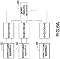
- FIG. 6A to FIG. 6C show block diagrams of the power supply system operating in different applications according to the present disclosure.
- each of a plurality of power supply apparatuses 100 with outputs connected in series is connected to the corresponding logic disconnection circuits 10, self-boosting circuits 20, protection circuits 30, and current sensing units 40 to form a single-string structure, and then connected to the power receiving apparatus 200.
- FIG. 6B multiple single-string structures shown in FIG. 6A are connected to the power receiving apparatus 200.
- FIG. 6C every two of a plurality of power supply apparatuses 100 with outputs connected in series are connected to the same logic disconnection circuit 10, self-boosting circuit, protection circuit 30, and current sensing unit 40, and then connected to the power receiving apparatus 200.
Landscapes
- Engineering & Computer Science (AREA)
- Power Engineering (AREA)
- Dc-Dc Converters (AREA)
- Emergency Protection Circuit Devices (AREA)
- Direct Current Feeding And Distribution (AREA)
Description
- The present disclosure relates to a power supply system with self-excited drive function, and more particularly to a power supply system with self-excited drive function that enables and disables a self-boosting operation according to whether a load draws current or not.
- The statements in this section merely provide background information related to the present disclosure and do not necessarily constitute prior art.
- The power supply apparatus of the power supply system is used to supply the required power to a load. If the distance between the load and the power supply apparatus is far, a disconnection apparatus is usually installed between the load and the power supply apparatus to avoid hazard to personnel safety and damage to equipment protection since there is still electricity on transmission lines between the power supply apparatus and the load once the load occurs abnormality or the load is not ready to receive the power electricity. Document
US 2018/366945 discloses a protection circuit for such a power supply apparatus. - The conventional disconnection apparatus may operate in the following manners. 1. Both the load and the shutdown apparatus need additional communication units, and the communication units are coupled and communicate to each other by a signal line. 2. The shutdown apparatus is a manual switch, and the operator manipulates the shutdown apparatus according to the condition of the load. No matter which manner is used, the costs of the power supply system, including labor cost, circuit cost, and so forth are significantly increased. Therefore, the present disclosure provides a safety shutdown apparatus with self-driving control.
- An object of the present disclosure is to provide a power supply system with self-excited drive to solve the problems of existing technology.
- In order to achieve the above-mentioned object, the power supply system with self-excited drive function is coupled to a power receiving apparatus through a positive power wire and a negative power wire. The power supply system includes a power supply apparatus, a logic disconnection circuit, a self-boosting circuit, a protection circuit, and a current sensing unit. The power supply apparatus outputs a DC power source between the positive power wire and the negative power wire. The logic disconnection circuit is coupled between the positive power wire and the negative power wire. The self-boosting circuit is coupled between the positive power wire and the negative power wire, and converts a voltage between the positive power wire and the negative power wire into an auxiliary voltage, and a receiving end of the self-boosting circuit is coupled to an output end of the logic disconnection circuit. The protection circuit is coupled between the positive power wire and the negative power wire, and is coupled to the self-boosting circuit to receive the auxiliary voltage. The current sensing unit is coupled to the positive power wire or the negative power wire, and outputs a current sensing signal according to a current flowing through the positive power wire or the negative power wire. The protection circuit makes a short circuit or an open circuit between the positive power wire and the negative power wire according to the current sensing signal, and the logic disconnection circuit disables or enables the self-boosting circuit according to the voltage between the positive power wire and the negative power wire.
- In one embodiment, when the current sensing signal is a first level, the protection circuit makes the positive power wire and the negative power wire be short-circuited; when the current sensing signal is a second level, the protection circuit makes the positive power wire and the negative power wire be open-circuited.
- In one embodiment, the protection circuit includes a switch coupled between the positive power wire and the negative power wire; when the switch is turned on, the positive power wire and the negative power wire are short-circuited; when the switch is turned off, the positive power wire and the negative power wire are open-circuited.
- In one embodiment, the protection circuit includes a first switch coupled between the positive power wire and the negative power wire, and a second switch coupled to the positive power wire or the negative power wire; the first switch and the second switch are complementarily controlled.
- In one embodiment, the self-boosting circuit includes a transistor switch, a coupling coil, and a capacitor. The coupling coil has two magnetically coupled coils, wherein one end of each of the two coils is commonly coupled to each other, and the other end of each of the two coils is respectively coupled to a base and a collector of the transistor switch. The capacitor is coupled to the collector of the transistor switch, and provides the auxiliary voltage.
- In one embodiment, the self-boosting circuit further includes a switch component; a control end of the switch component is the receiving end of the self-boosting circuit; the logic disconnection circuit disables the self-boosting circuit by turning off the switch component.
- In one embodiment, the switch component is coupled between the positive power wire and the coupling coil.
- In one embodiment, the switch component is coupled between the negative power wire and the coupling coil.
- In one embodiment, the logic disconnection circuit disables the self-boosting circuit when the voltage between the positive power wire and the negative power wire is greater than a threshold voltage value.
- In one embodiment, the self-boosting circuit further includes a diode; the diode is coupled between the positive power wire and the capacitor.
- In one embodiment, the protection circuit further includes a diode; the diode is coupled to the switch in series.
- In one embodiment, the power supply apparatus is a solar panel.
- In one embodiment, the current sensing unit is a Hall sensor, and receives the auxiliary voltage.
- Accordingly, the power supply system with self-excited drive function uses the protection circuit to provide a short-circuited path to limit the output voltage of the power supply apparatus to ensure the safety of the operators and protecting the equipment when the power receiving apparatus has not drawn current yet, and uses the self-boosting circuit to boost a small voltage to a large voltage to maintain sufficient voltage for supplying the protection circuit and the current sensing unit with a higher voltage to make them normally operate.
- It is to be understood that both the foregoing general description and the following detailed description are exemplary, and are intended to provide further explanation of the present disclosure as claimed. Other advantages and features of the present disclosure will be apparent from the following description, drawings and claims.
- The present disclosure can be more fully understood by reading the following detailed description of the embodiment, with reference made to the accompanying drawing as follows:
-
FIG. 1 is a block diagram of a power supply system with self-excited drive function according to the present disclosure. -
FIG. 2 is a block circuit diagram of the power supply system according to a first embodiment of the present disclosure. -
FIG. 3 is a block circuit diagram of the power supply system according to a second embodiment of the present disclosure. -
FIG. 4 is a block circuit diagram of the power supply system according to a third embodiment of the present disclosure. -
FIG. 5A to FIG. 5C are circuit diagrams of a protection circuit cooperated with a current sensing unit according to different embodiments of the present disclosure. -
FIG. 6A to FIG. 6C are block diagrams of the power supply system operating in different applications according to the present disclosure. - Reference will now be made to the drawing figures to describe the present disclosure in detail. It will be understood that the drawing figures and exemplified embodiments of present disclosure are not limited to the details thereof.
- Please refer to
FIG. 1 , which shows a block diagram of a power supply system with self-excited drive function according to the present disclosure. The power supply system with self-excited drive function (hereinafter referred to as "power supply system") includes apower supply apparatus 100, alogic disconnection circuit 10, a self-boosting circuit 20, aprotection circuit 30, and acurrent sensing unit 40, and supplies power to apower receiving apparatus 200. In one embodiment, thepower supply apparatus 100 is an apparatus that provides DC power output. - As shown in
FIG. 1 , thepower receiving apparatus 200 is coupled to thepower supply apparatus 100 through a positive power wire Lp+ and a negative power wire Lp-. Thelogic disconnection circuit 10 is coupled between the positive power wire Lp+ and the negative power wire Lp-. The self-boosting circuit 20 is coupled between the positive power wire Lp+ and the negative power wire Lp-, and a receiving end of the self-boosting circuit 20 is coupled to an output end of thelogic disconnection circuit 10. Theprotection circuit 30 is coupled between the positive power wire Lp+ and the negative power wire Lp-, and theprotection circuit 30 is coupled to an output end of the self-boosting circuit 20. Thecurrent sensing unit 40 is coupled to the positive power wire Lp+ or the negative power wire Lp-, and detects a current flowing through the positive power wire Lp+ or the negative power wire Lp-. In this embodiment shown inFIG. 1 , thecurrent sensing unit 40 is coupled to the positive power wire Lp+. - The
power supply apparatus 100 is a power apparatus that can output DC power. In the following, a solar panel is used as thepower supply apparatus 100 and a solar inverter is used as thepower receiving apparatus 200 as an example. When the solar inverter used in construction with the solar panel is in an unprepared condition, or the solar inverter needs to be urgently powered off (for example, repairs, fire, or other abnormal conditions), in order to prevent the continuous output of the DC power from the solar panel from causing casualties, theprotection circuit 30 can make the positive power wire Lp+ and the negative power wire Lp- be short-circuited so that the voltage provided to the solar inverter is reduced to a very small voltage value, such as about 1 volt. Therefore, it is to ensure the probability and degree of equipment loss and personal injury are minimized. Thepower supply apparatus 100 may also be, for example, a power supply with a high-voltage DC output that can supply power to a remote small base station, and thepower receiving apparatus 200 may be a communication facility such as a small base station. When thepower receiving apparatus 200 does not completely draw current (for example, repairs or other abnormal conditions), theprotection circuit 30 can be also used to ensure that the voltage of thepower receiving apparatus 200 reaches a safe voltage. - Hereinafter, the operation of the power supply system of the present disclosure will be described. Please refer to
FIG. 2 , which shows a block circuit diagram of the power supply system according to a first embodiment of the present disclosure. When thepower supply apparatus 100 has not outputted voltage and thepower receiving apparatus 200 is unprepared (not ready), a current Ia flowing through a power supply path Ps is zero, and the components of the entire power supply system have no power and thecurrent sensing unit 40 will not sense current. - When the
power supply apparatus 100 starts to output voltage, such as a 10-volt DC voltage (for the convenience of explanation), the current Ia flowing through the power supply path Ps is still zero since thepower receiving apparatus 200 is unprepared and thepower receiving apparatus 200 does not draw current. At this condition, the voltage outputted from thepower supply apparatus 100 provides the power required by the components of the power supply system. Thecurrent sensing unit 40 outputs a current sensing signal Is with a first level, such as a low level according to the current Ia flowing through the power supply path Ps. Since a switch S1 of theprotection circuit 30 is turned on according to the current sensing signal Is, a short circuit is formed between the positive power wire Lp+ and the negative power wire Lp-, except for a cross voltage (about 1 volt, which may be adjusted by increasing or decreasing the number of diodes) provided by a diode D11 and the switch S1. - The small voltage of 1 volt may not be able to maintain sufficient voltage for the protection circuit 30 (including the operational amplifier and/or other components) and the
current sensing unit 40 since the components generally require a higher supply voltage. To solve this problem, it is necessary to select components with special specifications, which leads to difficulties in component selection and increased costs. Therefore, the self-boostingcircuit 20 boosts (steps up) the small voltage of 1 volt to a large voltage of 5 to 10 volts, that is, an auxiliary voltage Va of a capacitor C12 of the self-boostingcircuit 20 is built up to maintain sufficient voltage for supplying theprotection circuit 30 and thecurrent sensing unit 40 with a higher voltage to make them normally operate. - In this embodiment, the self-boosting
circuit 20 is coupled to the positive power wire Lp+ through a normally-closed relay so that the small voltage of 1 volt is provided to the self-boostingcircuit 20 for self-excited boost. A control end of the relay RLY is used as a receiving end of the self-boostingcircuit 20 and is coupled to an output end of thelogic disconnection circuit 10. The self-boostingcircuit 20 includes a switch Q12 (i.e., a transistor switch in this embodiment) and a coupling coil L11. The coupling coil L11 has two magnetically coupled coils. One end of each of the two coils is commonly coupled to each other and coupled to the positive power wire Lp+, and the other end of each of the two coils is respectively coupled to a base and a collector of the switch Q12. The small voltage of 1 volt generates a base current IB flowing to the base of the switch Q12 and a collector current Ic flowing to the collector of the switch Q12 through the coupling coil L11, and IC=βIB. When the base current IB starts to increase, the collector current IC also increases, and therefore the coupling coil L11 starts to store energy. Once the collector current IC becomes larger to cause the β value to decrease so that IC<βIB, the switch Q12 enters the saturation region and then enters the cutoff region, thereby turning off the switch Q12. At this condition, the energy stored in the coupling coil L11 releases to charge the capacitor C12 through a path including the diode D12 and the capacitor C12 so that the auxiliary voltage Va increases. Therefore, the function of the self-boostingcircuit 20 is similar to a boost converter. In other words, the self-boostingcircuit 20 converts a voltage between the positive power wire Lp+ and the negative power wire Lp- into the auxiliary voltage Va to supply power to theprotection circuit 30 and thecurrent sensing unit 40. - When the energy stored in the coupling coil L11 is completely released, the base current IB flows again and the collector current IC increases again. Therefore, the repeated energy-storing and energy-releasing operations of the coupling coil L11 to achieve the energy storage and energy release of the exciting current through the switching action of self-excited oscillation. Accordingly, the small voltage of 1 volt is boosted (stepped up) to a large voltage of 5 to 10 volts, that is, the auxiliary voltage Va is gradually increased to maintain sufficient voltage for supplying the
protection circuit 30 and thecurrent sensing unit 40 with a higher voltage to make them normally operate. The above-mentioned situation is that thepower receiving apparatus 200 does not draw current or has not drawn current yet, and there is a small voltage between the positive power wire Lp+ and the negative power wire Lp- which is the same as a short circuit. - When the
power receiving apparatus 200 starts to draw current, that is, thepower receiving apparatus 200 starts to operate, the current Ia flowing through the power supply path Ps is no longer zero since the small voltage exists between the positive power wire Lp+ and the negative power wire Lp-. Thecurrent sensing unit 40 outputs a current sensing signal Is with a second level, such as a high level according to the current Ia flowing through the power supply path Ps. Since the switch S1 of theprotection circuit 30 is turned off according to the current sensing signal Is, an open circuit is formed between the positive power wire Lp+ and the negative power wire Lp-. Since the positive power wire Lp+ and the negative power wire Lp- are not short-circuited, the power required by theprotection circuit 30 and thecurrent sensing unit 40 no longer needs to be provided by the self-boostingcircuit 20. Therefore, thelogic disconnection circuit 10 disables the self-boostingcircuit 20, and thepower supply apparatus 100 provides the required power, such as 10-volt voltage outputted from thepower supply apparatus 100, for theprotection circuit 30 and thecurrent sensing unit 40. - Specifically, the 10-volt voltage outputted from the
power supply apparatus 100 is divided by resistors R12, R13 to acquire a divided voltage to turn on the switch Q13. Also, the 10-volt voltage is divided by resistors R14, R15 to acquire to divided voltage to turn on the switch Q14. In addition, the Zener diode D14 provides a fixed voltage to turn on the switch Q15 and then to build a voltage on the capacitor C13. The voltage (capacitor voltage) is coupled to the coil of the relay RLY, and when the coil induces voltage, the relay RLY is activated to open. Therefore, a connection path between the positive power wire Lp+ and the self-boostingcircuit 20 is disconnected so that the boost operation of the self-boostingcircuit 20 is disabled due to no energy-storing path and energy-releasing path in the coupling coil L11. In other words, the self-boostingcircuit 20 is coupled to the output end of thelogic disconnection circuit 10 through the relay RLY, and therefore thelogic disconnection circuit 10 can disable the self-boostingcircuit 20 through the output end. - At this condition, the 10-volt voltage outputted from the
power supply apparatus 100 charges the capacitor C12 through the diode D13. In other words, the diode D13 provides a path of charging the capacitor C12 so that the capacitor C12 can provide the sufficient auxiliary voltage Va to continuously supply power to theprotection circuit 30 and thecurrent sensing unit 40 after the self-boostingcircuit 20 is disabled. - Please refer to
FIG. 3 , which shows a block circuit diagram of the power supply system according to a second embodiment of the present disclosure. The major difference between the second embodiment and the first embodiment shown inFIG. 2 is that thelogic disconnection circuits 10 are different. The self-boostingcircuit 20 is coupled to the negative power wire Lp- through a switch Q22, and a control end of the switch Q22 is used as a receiving end of the self-boostingcircuit 20 and is coupled to thelogic disconnection circuit 10. As mentioned above, when thepower receiving apparatus 200 does not draw current, the switch S1 of theprotection circuit 30 is turned on so that a short circuit is formed between the positive power wire Lp+ and the negative power wire Lp-. Therefore, a small voltage of 1 volt turns on the switch Q22 through the resistor R23, however, a voltage divided by resistors R21, R22 is not enough to turn on the switch Q21, so that the self-boostingcircuit 20 is enabled to be self-excited activated. The principle of boost operation is as mentioned above and the detail description is omitted here for conciseness. Therefore, the self-boostingcircuit 20 boosts (steps up) the small voltage of 1 volt to a large voltage of 5 to 10 volts to maintain sufficient voltage for supplying theprotection circuit 30 and thecurrent sensing unit 40 with a higher voltage to make them normally operate. - When the
power receiving apparatus 200 starts to draw current, the current Ia flowing through the power supply path Ps is no longer zero. Since the switch S1 of theprotection circuit 30 is turned off, an open circuit is formed between the positive power wire Lp+ and the negative power wire Lp-. Since the positive power wire Lp+ and the negative power wire Lp- are not short-circuited, the power required by theprotection circuit 30 and thecurrent sensing unit 40 no longer needs to be provided by the self-boostingcircuit 20. Therefore, thelogic disconnection circuit 10 disables the self-boostingcircuit 20, and thepower supply apparatus 100 provides the required power, such as 10-volt voltage outputted from thepower supply apparatus 100, for theprotection circuit 30 and thecurrent sensing unit 40. - Specifically, the 10-volt voltage outputted from the
power supply apparatus 100 is divided by resistors R21, R22 to acquire a divided voltage to turn on the switch Q21. Since the switch Q21 is connected to a gate and a source of a switch Q22 (take MOS as an example), the switch Q22 is turned off by a gate-source voltage of zero volt due to the turned-on switch Q21. Since the switch Q22 is turned off, a connection path between the negative power wire Lp- and the self-boostingcircuit 20 is disconnected so that the boost operation of the self-boostingcircuit 20 is disabled due to no energy-storing path and energy-releasing path in the coupling coil L11. - At this condition, the 10-volt voltage outputted from the
power supply apparatus 100 charges the capacitor C12 through the diode D13. In other words, the diode D13 provides a path of charging the capacitor C12 so that the capacitor C12 can provide the sufficient auxiliary voltage Va to continuously supply power to theprotection circuit 30 and thecurrent sensing unit 40 after the self-boostingcircuit 20 is disabled. - Please refer to
FIG. 4 , which shows a block circuit diagram of the power supply system according to a third embodiment of the present disclosure. The major difference between the third embodiment and the first embodiment shown inFIG. 2 is that thelogic disconnection circuits 10 are different. As mentioned above, when thepower receiving apparatus 200 does not draw current, the switch S1 of theprotection circuit 30 is turned on so that a short circuit is formed between the positive power wire Lp+ and the negative power wire Lp-. Therefore, a small voltage of 1 volt provides a voltage Vb through resistors R35, R36 to turn on the switch Q33 so that the self-boostingcircuit 20 is enabled to be self-excited activated. The principle of boost operation is as mentioned above and the detail description is omitted here for conciseness. Therefore, the self-boostingcircuit 20 boosts (steps up) the small voltage of 1 volt to a large voltage of 5 to 10 volts to maintain sufficient voltage for supplying theprotection circuit 30 and thecurrent sensing unit 40 with a higher voltage to make them normally operate. - When the
power receiving apparatus 200 starts to draw current, the current Ia flowing through the power supply path Ps is no longer zero. Since the switch S1 of theprotection circuit 30 is turned off, an open circuit is formed between the positive power wire Lp+ and the negative power wire Lp-. Since the positive power wire Lp+ and the negative power wire Lp- are not short-circuited, the power required by theprotection circuit 30 and thecurrent sensing unit 40 no longer needs to be provided by the self-boostingcircuit 20. Therefore, thelogic disconnection circuit 10 disables the self-boostingcircuit 20, and thepower supply apparatus 100 provides the required power, such as 10-volt voltage outputted from thepower supply apparatus 100, for theprotection circuit 30 and thecurrent sensing unit 40. - Specifically, the 10-volt voltage outputted from the
power supply apparatus 100 is divided by resistors R31, R32 to acquire a divided voltage to turn on the switch Q31 (take n-MOS as an example); the 10-volt voltage is also divided by resistors R33, R34 to acquire a divided voltage to turn on the switch Q32 (take p-MOS as an example). At this condition, the voltage Vb is 10 volts at the positive power wire Lp+ to turn off the switch Q33 (take p-MOS as an example). Since the switch Q33 is turned off, a connection path between the positive power wire Lp+ and the self-boostingcircuit 20 is disconnected so that the boost operation of the self-boostingcircuit 20 is disabled due to no energy-storing path and energy-releasing path in the coupling coil L11. - At this condition, the 10-volt voltage outputted from the
power supply apparatus 100 charges the capacitor C12 through the diode D13. In other words, the diode D13 provides a path of charging the capacitor C12 so that the capacitor C12 can provide the sufficient auxiliary voltage Va to continuously supply power to theprotection circuit 30 and thecurrent sensing unit 40 after the self-boostingcircuit 20 is disabled. - According to the description of
FIG. 2 to FIG. 4 , thelogic disconnection circuit 10 disables or enables the self-boostingcircuit 20 according to the voltage between the positive power wire Lp+ and the negative power wire Lp-, and therefore the circuit parameters, such as resistance values of thelogic disconnection circuit 10 can be adjusted to determine conditions for disabling the self-boostingcircuit 20. For example, the self-boostingcircuit 20 is disabled when the voltage between the positive power wire Lp+ and the negative power wire Lp- is greater than a predetermined threshold voltage value so as to ensure that the components of the power supply system can acquire the sufficient voltage supply. - Please refer to
FIG. 5A to FIG. 5C , which show circuit diagrams of a protection circuit cooperated with a current sensing unit according to different embodiments of the present disclosure, and also refer toFIG. 1 . In comparison with the protection circuit 30 (having only one switch S1) shown inFIG. 2 to FIG. 4 , theprotection circuit 30 shown inFIG. 5A has two switches S1, S2 as theprotection circuit 30, and a sensing resistor RS is cooperated with a differential amplifier as thecurrent sensing unit 40. In particular, the two switches S1, S2 are complementarily controlled, that is, one is turned on and the other is turned off. When thepower receiving apparatus 200 does not draw current (i.e., the current Ia is zero), a voltage difference Vab between two ends of the sensing resistor RS is zero, and therefore a voltage V2 of the current sensing signal Is is low level. Since the reference voltage Vref is greater than the voltage V2, a voltage V3 is high level so that the switch S1 is turned on and the switch S2 is turned off. On the contrary, when thepower receiving apparatus 200 starts to draw current (i.e., the current Ia is not zero), the voltage difference Vab between the two ends of the sensing resistor RS is not zero, and therefore the voltage V2 of the current sensing signal Is is high level. Since the reference voltage Vref is less than the voltage V2, the voltage V3 is low level so that the switch S1 is turned off and the switch S2 is turned on. - In comparison with
FIG. 5A of using the sensing resistor RS to sense the current la, a current transformer or a Hall sensor is used as thecurrent sensing unit 40 to direct sense the current Ia inFIG. 5B without using the differential amplifier. Also, the current transformer does not require power supply to output the current sensing signal Is by the induced current or voltage due to the current flowing through the current transformer. When thepower receiving apparatus 200 does not draw current (i.e., the current Ia is zero), thecurrent sensing unit 40 outputs the voltage V2 with low level. Since the reference voltage Vref is greater than the voltage V2, the voltage V3 is high level so that the switch S1 is turned on and the switch S2 is turned off. On the contrary, when thepower receiving apparatus 200 starts to draw current (i.e., the current Ia is not zero), thecurrent sensing unit 40 outputs the voltage V2 with high level. Since the reference voltage Vref is less than the voltage V2, the voltage V3 is low level so that the switch S1 is turned off and the switch S2 is turned on. - The
protection circuit 30 shown inFIG. 5C has two switches Q1, S1 as theprotection circuit 30. When thepower receiving apparatus 200 does not draw current (i.e., the current Ia is zero), the 10-volt voltage outputted from thepower supply apparatus 100 turns on the switch S1 and there is a small voltage between the positive power wire Lp+ and the negative power wire Lp- which is the same as a short circuit. The small voltage supplies power to thecurrent sensing unit 40, and if the current sensing current 40 requires a larger voltage, it can be powered by the self-boostingcircuit 20. When thepower receiving apparatus 200 starts to draw current, the current sensing signal Is outputted from thecurrent sensing unit 40 controls the switch Q1 to be turned on. At this condition, a voltage Vd coupled to a gate of the switch S1 is zero volt so that the switch S1 is turned off, and therefore an open circuit is formed between the positive power wire Lp+ and the negative power wire Lp-. In this embodiment, since the resistance of the resistor R1 is relatively large, the current Ia will flow to thepower receiving apparatus 200. In addition, the diode D1 can be replaced by a Zener diode, a transient voltage suppressor, or a regulator IC to control a voltage of driving the switch S1. - Please refer to
FIG. 6A to FIG. 6C , which show block diagrams of the power supply system operating in different applications according to the present disclosure. As shown inFIG. 6A , each of a plurality ofpower supply apparatuses 100 with outputs connected in series is connected to the correspondinglogic disconnection circuits 10, self-boostingcircuits 20,protection circuits 30, andcurrent sensing units 40 to form a single-string structure, and then connected to thepower receiving apparatus 200. As shown inFIG. 6B , multiple single-string structures shown inFIG. 6A are connected to thepower receiving apparatus 200. As shown inFIG. 6C , every two of a plurality ofpower supply apparatuses 100 with outputs connected in series are connected to the samelogic disconnection circuit 10, self-boosting circuit,protection circuit 30, andcurrent sensing unit 40, and then connected to thepower receiving apparatus 200. - In conclusion, the present disclosure has following features and advantages:
- 1. Since the absence of the communication unit, the communication wires, and the communication protocol for the
protection circuit 30, the present disclosure can effectively save the circuit cost and simplify the design of the control circuit. - 2. When the
power receiving apparatus 200 has not drawn current yet, theprotection circuit 30 provides a short-circuited path to limit the output voltage of thepower supply apparatus 100, thereby ensuring the safety of the operators and protecting the equipment. - 3. When the
power receiving apparatus 200 has not drawn current yet, the self-boostingcircuit 20 boosts (steps up) the small voltage of 1 volt to a large voltage of 5 to 10 volts to maintain sufficient voltage for supplying theprotection circuit 30 and thecurrent sensing unit 40 with a higher voltage to make them normally operate. - 4. When the
power receiving apparatus 200 starts to draw current, thelogic disconnection circuit 10 disables the self-boostingcircuits 20 so that thepower supply apparatus 100 can directly provide the required power for theprotection circuit 30 and thecurrent sensing unit 40.
Claims (13)
- A power supply system with self-excited drive function coupled to a power receiving apparatus (200) through a positive power wire (Lp+) and a negative power wire (Lp-), characterized in that the power supply system comprising:a power supply apparatus (100) configured to output a DC power source between the positive power wire (Lp+) and the negative power wire (Lp-),a logic disconnection circuit (10) coupled between the positive power wire (Lp+) and the negative power wire (Lp-),a self-boosting circuit (20) coupled between the positive power wire (Lp+) and the negative power wire (Lp-), and configured to convert a voltage between the positive power wire (Lp+) and the negative power wire (Lp-) into an auxiliary voltage (Va), and a receiving end of the self-boosting circuit (20) coupled to an output end of the logic disconnection circuit (10),a protection circuit (30) coupled between the positive power wire (Lp+) and the negative power wire (Lp-), and coupled to the self-boosting circuit (20) to receive the auxiliary voltage (Va), anda current sensing unit (40) coupled to the positive power wire (Lp+) or the negative power wire (Lp-), and configured to output a current sensing signal (Is) according to a current flowing through the positive power wire (Lp+) or the negative power wire (Lp-),wherein the protection circuit (30) makes a short circuit or an open circuit between the positive power wire (Lp+) and the negative power wire (Lp-) according to the current sensing signal (Is), and the logic disconnection circuit (10) disables or enables the self-boosting circuit (20) according to the voltage between the positive power wire (Lp+) and the negative power wire (Lp-).
- The power supply system with self-excited drive function as claimed in claim 1, wherein when the current sensing signal (Is) is a first level, the protection circuit (30) makes the positive power wire (Lp+) and the negative power wire (Lp-) be short-circuited; when the current sensing signal (Is) is a second level, the protection circuit (30) makes the positive power wire (Lp+) and the negative power wire (Lp-) be open-circuited.
- The power supply system with self-excited drive function as claimed in claim 1, wherein the protection circuit (30) comprises a switch coupled between the positive power wire (Lp+) and the negative power wire (Lp-); when the switch is turned on, the positive power wire (Lp+) and the negative power wire (Lp-) are short-circuited; when the switch is turned off, the positive power wire (Lp+) and the negative power wire (Lp-) are open-circuited.
- The power supply system with self-excited drive function as claimed in claim 1, wherein the protection circuit (30) comprises a first switch (S1) coupled between the positive power wire (Lp+) and the negative power wire (Lp-), and a second switch (S2) coupled to the positive power wire (Lp+) or the negative power wire (Lp-); wherein the first switch (S1) and the second switch (S2) are complementarily controlled.
- The power supply system with self-excited drive function as claimed in claim 1, wherein the self-boosting circuit (20) comprises:a transistor switch (Q12),a coupling coil (L11) having two magnetically coupled coils, wherein one end of each of the two coils is commonly coupled to each other, and the other end of each of the two coils is respectively coupled to a base and a collector of the transistor switch (Q12), anda capacitor (C12) coupled to the collector of the transistor switch (Q12), and configured to provide the auxiliary voltage (Va).
- The power supply system with self-excited drive function as claimed in claim 5, wherein the self-boosting circuit (20) further comprises a switch component (RLY, Q22, Q33); a control end of the switch component (RLY, Q22, Q33) is the receiving end of the self-boosting circuit (20); the logic disconnection circuit (10) disables the self-boosting circuit (20) by turning off the switch component (RLY, Q22, Q33).
- The power supply system with self-excited drive function as claimed in claim 6, wherein the switch component (RLY, Q33) is coupled between the positive power wire (Lp+) and the coupling coil (L11).
- The power supply system with self-excited drive function as claimed in claim 6, wherein the switch component (Q22) is coupled between the negative power wire (Lp-) and the coupling coil (L11).
- The power supply system with self-excited drive function as claimed in claim 1, wherein the logic disconnection circuit (10) disables the self-boosting circuit (20) when the voltage between the positive power wire (Lp+) and the negative power wire (Lp-) is greater than a threshold voltage value.
- The power supply system with self-excited drive function as claimed in claim 5, wherein the self-boosting circuit (20) further comprises:
a diode (D13) coupled between the positive power wire (Lp+) and the capacitor (C12). - The power supply system with self-excited drive function as claimed in claim 3, wherein the protection circuit (30) further comprises:
a diode (D11) coupled to the switch (S1) in series. - The power supply system with self-excited drive function as claimed in claim 1, wherein the power supply apparatus (100) is a solar panel.
- The power supply system with self-excited drive function as claimed in claim 1, wherein the current sensing unit (40) is a Hall sensor, and receives the auxiliary voltage (Va).
Applications Claiming Priority (2)
| Application Number | Priority Date | Filing Date | Title |
|---|---|---|---|
| US202063062906P | 2020-08-07 | 2020-08-07 | |
| US17/166,369 US11699948B2 (en) | 2020-08-07 | 2021-02-03 | Power supply system with self-excited drive function |
Publications (2)
| Publication Number | Publication Date |
|---|---|
| EP3952086A1 EP3952086A1 (en) | 2022-02-09 |
| EP3952086B1 true EP3952086B1 (en) | 2022-10-19 |
Family
ID=76250241
Family Applications (1)
| Application Number | Title | Priority Date | Filing Date |
|---|---|---|---|
| EP21177457.5A Active EP3952086B1 (en) | 2020-08-07 | 2021-06-02 | Power supply system with self-excited drive function |
Country Status (6)
| Country | Link |
|---|---|
| US (1) | US11699948B2 (en) |
| EP (1) | EP3952086B1 (en) |
| JP (1) | JP7108093B2 (en) |
| CN (1) | CN114070077A (en) |
| ES (1) | ES2930052T3 (en) |
| TW (1) | TWI742995B (en) |
Family Cites Families (20)
| Publication number | Priority date | Publication date | Assignee | Title |
|---|---|---|---|---|
| NL8202259A (en) | 1982-06-04 | 1984-01-02 | Philips Nv | POWER SUPPLY CONTAINING AN AC POWER SUPPLY SOURCE, A LOAD AND A CONNECTION CABLE BETWEEN SOURCE AND LOAD. |
| WO1985000933A1 (en) * | 1983-08-11 | 1985-02-28 | Astec Components, Ltd. | Self-driven proportional dc-dc converter with overcurrent protection |
| JPH0720952A (en) | 1993-06-23 | 1995-01-24 | Canon Inc | Power unit |
| JP3205756B2 (en) * | 1997-07-22 | 2001-09-04 | 株式会社エスアイアイ・アールディセンター | Electronics |
| JPH1173231A (en) * | 1997-08-29 | 1999-03-16 | Sharp Corp | Dc stabilized power supply device |
| JP2011024303A (en) | 2009-07-14 | 2011-02-03 | Toyota Motor Corp | Charge/discharge control device |
| JP5683400B2 (en) * | 2011-07-22 | 2015-03-11 | 京セラ株式会社 | Power control apparatus and power system |
| DE102011110682A1 (en) | 2011-08-19 | 2013-02-21 | Phoenix Contact Gmbh & Co. Kg | Junction box for a solar panel with a protection circuit |
| EP2587670A1 (en) | 2011-10-26 | 2013-05-01 | ABB Technology AG | Control contact driving system |
| TWI432096B (en) * | 2011-12-27 | 2014-03-21 | Ind Tech Res Inst | Lamp control system, lamp power saving system and method therefor |
| TW201349731A (en) | 2012-05-30 | 2013-12-01 | Delta Electronics Inc | Photovoltaic power system with generation modules and method of controlling output power thereof |
| CN103841707B (en) * | 2012-11-26 | 2015-09-09 | 硕颉科技股份有限公司 | Be associated with the load drive device of light-emitting diode |
| TW201422053A (en) * | 2012-11-29 | 2014-06-01 | Beyond Innovation Tech Co Ltd | Load driving apparatus relating to light-emitting-diodes |
| TWI458233B (en) | 2013-01-07 | 2014-10-21 | Richtek Technology Corp | Switch power conversion device |
| CN105052027A (en) * | 2013-04-02 | 2015-11-11 | 三菱电机株式会社 | Power conversion apparatus and cooling air-conditioning apparatus |
| CN108695843B (en) * | 2017-03-29 | 2023-09-22 | 太阳能安吉科技有限公司 | Bypass circuit and method of bypassing power module in power system |
| CN107565528B (en) * | 2017-07-27 | 2019-03-12 | 郑州云海信息技术有限公司 | A kind of circuit structure inhibiting surge current |
| US11183863B2 (en) * | 2017-10-20 | 2021-11-23 | Honor Device Co., Ltd. | Charging apparatus and terminal |
| US11159084B2 (en) * | 2018-12-14 | 2021-10-26 | Infineon Technologies Ag | Protection circuit with a cut-off switch for power systems |
| CN109600039B (en) * | 2018-12-14 | 2021-05-18 | 广州金升阳科技有限公司 | Power supply circuit and photovoltaic power generation system comprising same |
-
2021
- 2021-02-03 US US17/166,369 patent/US11699948B2/en active Active
- 2021-02-05 CN CN202110162110.8A patent/CN114070077A/en active Pending
- 2021-02-05 TW TW110104395A patent/TWI742995B/en active
- 2021-05-31 JP JP2021091595A patent/JP7108093B2/en active Active
- 2021-06-02 ES ES21177457T patent/ES2930052T3/en active Active
- 2021-06-02 EP EP21177457.5A patent/EP3952086B1/en active Active
Also Published As
| Publication number | Publication date |
|---|---|
| US11699948B2 (en) | 2023-07-11 |
| CN114070077A (en) | 2022-02-18 |
| ES2930052T3 (en) | 2022-12-05 |
| JP7108093B2 (en) | 2022-07-27 |
| US20220045598A1 (en) | 2022-02-10 |
| EP3952086A1 (en) | 2022-02-09 |
| JP2022031126A (en) | 2022-02-18 |
| TWI742995B (en) | 2021-10-11 |
| TW202207568A (en) | 2022-02-16 |
Similar Documents
| Publication | Publication Date | Title |
|---|---|---|
| JP4729330B2 (en) | Switching power supply | |
| JP4400880B2 (en) | Lighting control circuit for vehicular lamp | |
| RU2374734C2 (en) | Guard circuit for sparkproof electromagnetic actuators and guard circuit for sparkproof electric power systems | |
| US10008952B1 (en) | Power conversion system with conditioner capacitor discharge apparatus | |
| EP3038223B1 (en) | Load driving circuit | |
| CN112928905A (en) | Pre-charging switch, power supply arrangement and method for connecting load to DC voltage source | |
| KR101260340B1 (en) | Emergency line bypass switching circuit of uninterruptiblepower supply | |
| US20120081816A1 (en) | Integrated variable output power supply protection circuit | |
| EP2482436A1 (en) | Insulation type switching power supply | |
| CN113506706B (en) | Contactor driving circuit with high reliability and working method | |
| EP3952086B1 (en) | Power supply system with self-excited drive function | |
| US9071079B2 (en) | Power supply system with multiple power sources in parallel | |
| CN116436268A (en) | Switching circuit suitable for low voltage application and vehicle | |
| EP4024689A1 (en) | Direct current bus capacitor breakdown protection circuit for drives | |
| US5291099A (en) | Neon sign power supply circuit with automatic power interruption | |
| CN103595024A (en) | Protection circuit of power supply | |
| JP2016149884A (en) | Dc power supply device | |
| KR20190104506A (en) | Power transfer control method using automatic power transfer control device with load short detection function | |
| KR100964597B1 (en) | Uninterrupted power supply | |
| US11600986B2 (en) | Safety shutdown apparatus with self-driven control, power supply system, and method of controlling the same | |
| CN217882822U (en) | Control circuit for load switch, driving circuit and lighting equipment | |
| CN212012118U (en) | Overvoltage protection circuit | |
| CN211456669U (en) | Short-circuit protection circuit for secondary voltage of intrinsic safety circuit | |
| KR101443320B1 (en) | Emergency line bypass switching circuit and power converter using the bypass switching circuit | |
| JP5297585B2 (en) | Device with protection against different voltage |
Legal Events
| Date | Code | Title | Description |
|---|---|---|---|
| PUAI | Public reference made under article 153(3) epc to a published international application that has entered the european phase |
Free format text: ORIGINAL CODE: 0009012 |
|
| STAA | Information on the status of an ep patent application or granted ep patent |
Free format text: STATUS: THE APPLICATION HAS BEEN PUBLISHED |
|
| STAA | Information on the status of an ep patent application or granted ep patent |
Free format text: STATUS: REQUEST FOR EXAMINATION WAS MADE |
|
| AK | Designated contracting states |
Kind code of ref document: A1 Designated state(s): AL AT BE BG CH CY CZ DE DK EE ES FI FR GB GR HR HU IE IS IT LI LT LU LV MC MK MT NL NO PL PT RO RS SE SI SK SM TR |
|
| 17P | Request for examination filed |
Effective date: 20220128 |
|
| RBV | Designated contracting states (corrected) |
Designated state(s): AL AT BE BG CH CY CZ DE DK EE ES FI FR GB GR HR HU IE IS IT LI LT LU LV MC MK MT NL NO PL PT RO RS SE SI SK SM TR |
|
| RIC1 | Information provided on ipc code assigned before grant |
Ipc: H02M 1/32 20070101AFI20220511BHEP |
|
| GRAP | Despatch of communication of intention to grant a patent |
Free format text: ORIGINAL CODE: EPIDOSNIGR1 |
|
| STAA | Information on the status of an ep patent application or granted ep patent |
Free format text: STATUS: GRANT OF PATENT IS INTENDED |
|
| INTG | Intention to grant announced |
Effective date: 20220722 |
|
| GRAS | Grant fee paid |
Free format text: ORIGINAL CODE: EPIDOSNIGR3 |
|
| GRAA | (expected) grant |
Free format text: ORIGINAL CODE: 0009210 |
|
| STAA | Information on the status of an ep patent application or granted ep patent |
Free format text: STATUS: THE PATENT HAS BEEN GRANTED |
|
| AK | Designated contracting states |
Kind code of ref document: B1 Designated state(s): AL AT BE BG CH CY CZ DE DK EE ES FI FR GB GR HR HU IE IS IT LI LT LU LV MC MK MT NL NO PL PT RO RS SE SI SK SM TR |
|
| REG | Reference to a national code |
Ref country code: GB Ref legal event code: FG4D |
|
| REG | Reference to a national code |
Ref country code: CH Ref legal event code: EP |
|
| REG | Reference to a national code |
Ref country code: IE Ref legal event code: FG4D |
|
| REG | Reference to a national code |
Ref country code: DE Ref legal event code: R096 Ref document number: 602021000580 Country of ref document: DE |
|
| REG | Reference to a national code |
Ref country code: AT Ref legal event code: REF Ref document number: 1526194 Country of ref document: AT Kind code of ref document: T Effective date: 20221115 |
|
| REG | Reference to a national code |
Ref country code: NL Ref legal event code: FP |
|
| REG | Reference to a national code |
Ref country code: ES Ref legal event code: FG2A Ref document number: 2930052 Country of ref document: ES Kind code of ref document: T3 Effective date: 20221205 |
|
| REG | Reference to a national code |
Ref country code: LT Ref legal event code: MG9D |
|
| REG | Reference to a national code |
Ref country code: AT Ref legal event code: MK05 Ref document number: 1526194 Country of ref document: AT Kind code of ref document: T Effective date: 20221019 |
|
| PG25 | Lapsed in a contracting state [announced via postgrant information from national office to epo] |
Ref country code: SE Free format text: LAPSE BECAUSE OF FAILURE TO SUBMIT A TRANSLATION OF THE DESCRIPTION OR TO PAY THE FEE WITHIN THE PRESCRIBED TIME-LIMIT Effective date: 20221019 Ref country code: PT Free format text: LAPSE BECAUSE OF FAILURE TO SUBMIT A TRANSLATION OF THE DESCRIPTION OR TO PAY THE FEE WITHIN THE PRESCRIBED TIME-LIMIT Effective date: 20230220 Ref country code: NO Free format text: LAPSE BECAUSE OF FAILURE TO SUBMIT A TRANSLATION OF THE DESCRIPTION OR TO PAY THE FEE WITHIN THE PRESCRIBED TIME-LIMIT Effective date: 20230119 Ref country code: LT Free format text: LAPSE BECAUSE OF FAILURE TO SUBMIT A TRANSLATION OF THE DESCRIPTION OR TO PAY THE FEE WITHIN THE PRESCRIBED TIME-LIMIT Effective date: 20221019 Ref country code: FI Free format text: LAPSE BECAUSE OF FAILURE TO SUBMIT A TRANSLATION OF THE DESCRIPTION OR TO PAY THE FEE WITHIN THE PRESCRIBED TIME-LIMIT Effective date: 20221019 Ref country code: AT Free format text: LAPSE BECAUSE OF FAILURE TO SUBMIT A TRANSLATION OF THE DESCRIPTION OR TO PAY THE FEE WITHIN THE PRESCRIBED TIME-LIMIT Effective date: 20221019 |
|
| PG25 | Lapsed in a contracting state [announced via postgrant information from national office to epo] |
Ref country code: RS Free format text: LAPSE BECAUSE OF FAILURE TO SUBMIT A TRANSLATION OF THE DESCRIPTION OR TO PAY THE FEE WITHIN THE PRESCRIBED TIME-LIMIT Effective date: 20221019 Ref country code: PL Free format text: LAPSE BECAUSE OF FAILURE TO SUBMIT A TRANSLATION OF THE DESCRIPTION OR TO PAY THE FEE WITHIN THE PRESCRIBED TIME-LIMIT Effective date: 20221019 Ref country code: LV Free format text: LAPSE BECAUSE OF FAILURE TO SUBMIT A TRANSLATION OF THE DESCRIPTION OR TO PAY THE FEE WITHIN THE PRESCRIBED TIME-LIMIT Effective date: 20221019 Ref country code: IS Free format text: LAPSE BECAUSE OF FAILURE TO SUBMIT A TRANSLATION OF THE DESCRIPTION OR TO PAY THE FEE WITHIN THE PRESCRIBED TIME-LIMIT Effective date: 20230219 Ref country code: HR Free format text: LAPSE BECAUSE OF FAILURE TO SUBMIT A TRANSLATION OF THE DESCRIPTION OR TO PAY THE FEE WITHIN THE PRESCRIBED TIME-LIMIT Effective date: 20221019 Ref country code: GR Free format text: LAPSE BECAUSE OF FAILURE TO SUBMIT A TRANSLATION OF THE DESCRIPTION OR TO PAY THE FEE WITHIN THE PRESCRIBED TIME-LIMIT Effective date: 20230120 |
|
| REG | Reference to a national code |
Ref country code: DE Ref legal event code: R097 Ref document number: 602021000580 Country of ref document: DE |
|
| PG25 | Lapsed in a contracting state [announced via postgrant information from national office to epo] |
Ref country code: SM Free format text: LAPSE BECAUSE OF FAILURE TO SUBMIT A TRANSLATION OF THE DESCRIPTION OR TO PAY THE FEE WITHIN THE PRESCRIBED TIME-LIMIT Effective date: 20221019 Ref country code: RO Free format text: LAPSE BECAUSE OF FAILURE TO SUBMIT A TRANSLATION OF THE DESCRIPTION OR TO PAY THE FEE WITHIN THE PRESCRIBED TIME-LIMIT Effective date: 20221019 Ref country code: EE Free format text: LAPSE BECAUSE OF FAILURE TO SUBMIT A TRANSLATION OF THE DESCRIPTION OR TO PAY THE FEE WITHIN THE PRESCRIBED TIME-LIMIT Effective date: 20221019 Ref country code: DK Free format text: LAPSE BECAUSE OF FAILURE TO SUBMIT A TRANSLATION OF THE DESCRIPTION OR TO PAY THE FEE WITHIN THE PRESCRIBED TIME-LIMIT Effective date: 20221019 Ref country code: CZ Free format text: LAPSE BECAUSE OF FAILURE TO SUBMIT A TRANSLATION OF THE DESCRIPTION OR TO PAY THE FEE WITHIN THE PRESCRIBED TIME-LIMIT Effective date: 20221019 |
|
| PLBE | No opposition filed within time limit |
Free format text: ORIGINAL CODE: 0009261 |
|
| STAA | Information on the status of an ep patent application or granted ep patent |
Free format text: STATUS: NO OPPOSITION FILED WITHIN TIME LIMIT |
|
| PG25 | Lapsed in a contracting state [announced via postgrant information from national office to epo] |
Ref country code: SK Free format text: LAPSE BECAUSE OF FAILURE TO SUBMIT A TRANSLATION OF THE DESCRIPTION OR TO PAY THE FEE WITHIN THE PRESCRIBED TIME-LIMIT Effective date: 20221019 Ref country code: AL Free format text: LAPSE BECAUSE OF FAILURE TO SUBMIT A TRANSLATION OF THE DESCRIPTION OR TO PAY THE FEE WITHIN THE PRESCRIBED TIME-LIMIT Effective date: 20221019 |
|
| 26N | No opposition filed |
Effective date: 20230720 |
|
| PGFP | Annual fee paid to national office [announced via postgrant information from national office to epo] |
Ref country code: IT Payment date: 20230630 Year of fee payment: 3 Ref country code: ES Payment date: 20230712 Year of fee payment: 3 |
|
| PG25 | Lapsed in a contracting state [announced via postgrant information from national office to epo] |
Ref country code: SI Free format text: LAPSE BECAUSE OF FAILURE TO SUBMIT A TRANSLATION OF THE DESCRIPTION OR TO PAY THE FEE WITHIN THE PRESCRIBED TIME-LIMIT Effective date: 20221019 |
|
| PG25 | Lapsed in a contracting state [announced via postgrant information from national office to epo] |
Ref country code: MC Free format text: LAPSE BECAUSE OF FAILURE TO SUBMIT A TRANSLATION OF THE DESCRIPTION OR TO PAY THE FEE WITHIN THE PRESCRIBED TIME-LIMIT Effective date: 20221019 |
|
| PG25 | Lapsed in a contracting state [announced via postgrant information from national office to epo] |
Ref country code: MC Free format text: LAPSE BECAUSE OF FAILURE TO SUBMIT A TRANSLATION OF THE DESCRIPTION OR TO PAY THE FEE WITHIN THE PRESCRIBED TIME-LIMIT Effective date: 20221019 |
|
| REG | Reference to a national code |
Ref country code: BE Ref legal event code: MM Effective date: 20230630 |
|
| PG25 | Lapsed in a contracting state [announced via postgrant information from national office to epo] |
Ref country code: LU Free format text: LAPSE BECAUSE OF NON-PAYMENT OF DUE FEES Effective date: 20230602 |
|
| REG | Reference to a national code |
Ref country code: IE Ref legal event code: MM4A |
|
| PG25 | Lapsed in a contracting state [announced via postgrant information from national office to epo] |
Ref country code: LU Free format text: LAPSE BECAUSE OF NON-PAYMENT OF DUE FEES Effective date: 20230602 |
|
| PG25 | Lapsed in a contracting state [announced via postgrant information from national office to epo] |
Ref country code: IE Free format text: LAPSE BECAUSE OF NON-PAYMENT OF DUE FEES Effective date: 20230602 |
|
| PG25 | Lapsed in a contracting state [announced via postgrant information from national office to epo] |
Ref country code: IE Free format text: LAPSE BECAUSE OF NON-PAYMENT OF DUE FEES Effective date: 20230602 |
|
| PG25 | Lapsed in a contracting state [announced via postgrant information from national office to epo] |
Ref country code: BE Free format text: LAPSE BECAUSE OF NON-PAYMENT OF DUE FEES Effective date: 20230630 |
|
| PGFP | Annual fee paid to national office [announced via postgrant information from national office to epo] |
Ref country code: NL Payment date: 20240515 Year of fee payment: 4 |
|
| PGFP | Annual fee paid to national office [announced via postgrant information from national office to epo] |
Ref country code: DE Payment date: 20240507 Year of fee payment: 4 |
|
| PGFP | Annual fee paid to national office [announced via postgrant information from national office to epo] |
Ref country code: FR Payment date: 20240509 Year of fee payment: 4 |