EP3952084A1 - Verfahren und vorrichtung zur effizienten umschaltung - Google Patents
Verfahren und vorrichtung zur effizienten umschaltung Download PDFInfo
- Publication number
- EP3952084A1 EP3952084A1 EP21189344.1A EP21189344A EP3952084A1 EP 3952084 A1 EP3952084 A1 EP 3952084A1 EP 21189344 A EP21189344 A EP 21189344A EP 3952084 A1 EP3952084 A1 EP 3952084A1
- Authority
- EP
- European Patent Office
- Prior art keywords
- switch
- controller
- voltage
- switches
- switching
- Prior art date
- Legal status (The legal status is an assumption and is not a legal conclusion. Google has not performed a legal analysis and makes no representation as to the accuracy of the status listed.)
- Pending
Links
- 238000000034 method Methods 0.000 title claims abstract description 48
- 230000000737 periodic effect Effects 0.000 claims abstract description 10
- 230000010363 phase shift Effects 0.000 claims description 6
- 238000013461 design Methods 0.000 abstract description 2
- 230000000875 corresponding effect Effects 0.000 description 20
- 230000008859 change Effects 0.000 description 15
- 238000005259 measurement Methods 0.000 description 8
- 230000008901 benefit Effects 0.000 description 7
- 230000000295 complement effect Effects 0.000 description 7
- 230000001276 controlling effect Effects 0.000 description 7
- 239000004065 semiconductor Substances 0.000 description 6
- 230000003071 parasitic effect Effects 0.000 description 4
- 230000008569 process Effects 0.000 description 4
- 230000009286 beneficial effect Effects 0.000 description 3
- 239000003990 capacitor Substances 0.000 description 3
- 238000012544 monitoring process Methods 0.000 description 3
- 230000000630 rising effect Effects 0.000 description 3
- 229910002601 GaN Inorganic materials 0.000 description 2
- 230000004075 alteration Effects 0.000 description 2
- 230000001747 exhibiting effect Effects 0.000 description 2
- 230000002349 favourable effect Effects 0.000 description 2
- 230000005669 field effect Effects 0.000 description 2
- 230000006872 improvement Effects 0.000 description 2
- 229910044991 metal oxide Inorganic materials 0.000 description 2
- 150000004706 metal oxides Chemical class 0.000 description 2
- 238000012986 modification Methods 0.000 description 2
- 230000004048 modification Effects 0.000 description 2
- HBMJWWWQQXIZIP-UHFFFAOYSA-N silicon carbide Chemical compound [Si+]#[C-] HBMJWWWQQXIZIP-UHFFFAOYSA-N 0.000 description 2
- 229910010271 silicon carbide Inorganic materials 0.000 description 2
- 230000000007 visual effect Effects 0.000 description 2
- JMASRVWKEDWRBT-UHFFFAOYSA-N Gallium nitride Chemical compound [Ga]#N JMASRVWKEDWRBT-UHFFFAOYSA-N 0.000 description 1
- 238000004378 air conditioning Methods 0.000 description 1
- 230000003190 augmentative effect Effects 0.000 description 1
- 238000001816 cooling Methods 0.000 description 1
- 230000002596 correlated effect Effects 0.000 description 1
- 238000006073 displacement reaction Methods 0.000 description 1
- 239000000446 fuel Substances 0.000 description 1
- 230000006870 function Effects 0.000 description 1
- 230000020169 heat generation Effects 0.000 description 1
- 230000007246 mechanism Effects 0.000 description 1
- 238000013021 overheating Methods 0.000 description 1
- 238000004806 packaging method and process Methods 0.000 description 1
- 238000005070 sampling Methods 0.000 description 1
- 229910000679 solder Inorganic materials 0.000 description 1
Images


Classifications
-
- H—ELECTRICITY
- H02—GENERATION; CONVERSION OR DISTRIBUTION OF ELECTRIC POWER
- H02M—APPARATUS FOR CONVERSION BETWEEN AC AND AC, BETWEEN AC AND DC, OR BETWEEN DC AND DC, AND FOR USE WITH MAINS OR SIMILAR POWER SUPPLY SYSTEMS; CONVERSION OF DC OR AC INPUT POWER INTO SURGE OUTPUT POWER; CONTROL OR REGULATION THEREOF
- H02M1/00—Details of apparatus for conversion
- H02M1/08—Circuits specially adapted for the generation of control voltages for semiconductor devices incorporated in static converters
- H02M1/088—Circuits specially adapted for the generation of control voltages for semiconductor devices incorporated in static converters for the simultaneous control of series or parallel connected semiconductor devices
-
- H—ELECTRICITY
- H02—GENERATION; CONVERSION OR DISTRIBUTION OF ELECTRIC POWER
- H02M—APPARATUS FOR CONVERSION BETWEEN AC AND AC, BETWEEN AC AND DC, OR BETWEEN DC AND DC, AND FOR USE WITH MAINS OR SIMILAR POWER SUPPLY SYSTEMS; CONVERSION OF DC OR AC INPUT POWER INTO SURGE OUTPUT POWER; CONTROL OR REGULATION THEREOF
- H02M1/00—Details of apparatus for conversion
- H02M1/0048—Circuits or arrangements for reducing losses
- H02M1/0054—Transistor switching losses
- H02M1/0058—Transistor switching losses by employing soft switching techniques, i.e. commutation of transistors when applied voltage is zero or when current flow is zero
-
- H—ELECTRICITY
- H02—GENERATION; CONVERSION OR DISTRIBUTION OF ELECTRIC POWER
- H02M—APPARATUS FOR CONVERSION BETWEEN AC AND AC, BETWEEN AC AND DC, OR BETWEEN DC AND DC, AND FOR USE WITH MAINS OR SIMILAR POWER SUPPLY SYSTEMS; CONVERSION OF DC OR AC INPUT POWER INTO SURGE OUTPUT POWER; CONTROL OR REGULATION THEREOF
- H02M3/00—Conversion of dc power input into dc power output
- H02M3/22—Conversion of dc power input into dc power output with intermediate conversion into ac
- H02M3/24—Conversion of dc power input into dc power output with intermediate conversion into ac by static converters
- H02M3/28—Conversion of dc power input into dc power output with intermediate conversion into ac by static converters using discharge tubes with control electrode or semiconductor devices with control electrode to produce the intermediate ac
- H02M3/325—Conversion of dc power input into dc power output with intermediate conversion into ac by static converters using discharge tubes with control electrode or semiconductor devices with control electrode to produce the intermediate ac using devices of a triode or a transistor type requiring continuous application of a control signal
- H02M3/335—Conversion of dc power input into dc power output with intermediate conversion into ac by static converters using discharge tubes with control electrode or semiconductor devices with control electrode to produce the intermediate ac using devices of a triode or a transistor type requiring continuous application of a control signal using semiconductor devices only
- H02M3/33507—Conversion of dc power input into dc power output with intermediate conversion into ac by static converters using discharge tubes with control electrode or semiconductor devices with control electrode to produce the intermediate ac using devices of a triode or a transistor type requiring continuous application of a control signal using semiconductor devices only with automatic control of the output voltage or current, e.g. flyback converters
- H02M3/33515—Conversion of dc power input into dc power output with intermediate conversion into ac by static converters using discharge tubes with control electrode or semiconductor devices with control electrode to produce the intermediate ac using devices of a triode or a transistor type requiring continuous application of a control signal using semiconductor devices only with automatic control of the output voltage or current, e.g. flyback converters with digital control
-
- H—ELECTRICITY
- H02—GENERATION; CONVERSION OR DISTRIBUTION OF ELECTRIC POWER
- H02M—APPARATUS FOR CONVERSION BETWEEN AC AND AC, BETWEEN AC AND DC, OR BETWEEN DC AND DC, AND FOR USE WITH MAINS OR SIMILAR POWER SUPPLY SYSTEMS; CONVERSION OF DC OR AC INPUT POWER INTO SURGE OUTPUT POWER; CONTROL OR REGULATION THEREOF
- H02M7/00—Conversion of ac power input into dc power output; Conversion of dc power input into ac power output
- H02M7/02—Conversion of ac power input into dc power output without possibility of reversal
- H02M7/04—Conversion of ac power input into dc power output without possibility of reversal by static converters
- H02M7/12—Conversion of ac power input into dc power output without possibility of reversal by static converters using discharge tubes with control electrode or semiconductor devices with control electrode
- H02M7/21—Conversion of ac power input into dc power output without possibility of reversal by static converters using discharge tubes with control electrode or semiconductor devices with control electrode using devices of a triode or transistor type requiring continuous application of a control signal
- H02M7/217—Conversion of ac power input into dc power output without possibility of reversal by static converters using discharge tubes with control electrode or semiconductor devices with control electrode using devices of a triode or transistor type requiring continuous application of a control signal using semiconductor devices only
- H02M7/219—Conversion of ac power input into dc power output without possibility of reversal by static converters using discharge tubes with control electrode or semiconductor devices with control electrode using devices of a triode or transistor type requiring continuous application of a control signal using semiconductor devices only in a bridge configuration
-
- H—ELECTRICITY
- H02—GENERATION; CONVERSION OR DISTRIBUTION OF ELECTRIC POWER
- H02M—APPARATUS FOR CONVERSION BETWEEN AC AND AC, BETWEEN AC AND DC, OR BETWEEN DC AND DC, AND FOR USE WITH MAINS OR SIMILAR POWER SUPPLY SYSTEMS; CONVERSION OF DC OR AC INPUT POWER INTO SURGE OUTPUT POWER; CONTROL OR REGULATION THEREOF
- H02M7/00—Conversion of ac power input into dc power output; Conversion of dc power input into ac power output
- H02M7/42—Conversion of dc power input into ac power output without possibility of reversal
- H02M7/44—Conversion of dc power input into ac power output without possibility of reversal by static converters
- H02M7/48—Conversion of dc power input into ac power output without possibility of reversal by static converters using discharge tubes with control electrode or semiconductor devices with control electrode
- H02M7/53—Conversion of dc power input into ac power output without possibility of reversal by static converters using discharge tubes with control electrode or semiconductor devices with control electrode using devices of a triode or transistor type requiring continuous application of a control signal
- H02M7/537—Conversion of dc power input into ac power output without possibility of reversal by static converters using discharge tubes with control electrode or semiconductor devices with control electrode using devices of a triode or transistor type requiring continuous application of a control signal using semiconductor devices only, e.g. single switched pulse inverters
- H02M7/5387—Conversion of dc power input into ac power output without possibility of reversal by static converters using discharge tubes with control electrode or semiconductor devices with control electrode using devices of a triode or transistor type requiring continuous application of a control signal using semiconductor devices only, e.g. single switched pulse inverters in a bridge configuration
-
- H—ELECTRICITY
- H03—ELECTRONIC CIRCUITRY
- H03K—PULSE TECHNIQUE
- H03K17/00—Electronic switching or gating, i.e. not by contact-making and –breaking
- H03K17/12—Modifications for increasing the maximum permissible switched current
-
- H—ELECTRICITY
- H03—ELECTRONIC CIRCUITRY
- H03K—PULSE TECHNIQUE
- H03K17/00—Electronic switching or gating, i.e. not by contact-making and –breaking
- H03K17/12—Modifications for increasing the maximum permissible switched current
- H03K17/122—Modifications for increasing the maximum permissible switched current in field-effect transistor switches
-
- H—ELECTRICITY
- H03—ELECTRONIC CIRCUITRY
- H03K—PULSE TECHNIQUE
- H03K2217/00—Indexing scheme related to electronic switching or gating, i.e. not by contact-making or -breaking covered by H03K17/00
- H03K2217/0036—Means reducing energy consumption
-
- Y—GENERAL TAGGING OF NEW TECHNOLOGICAL DEVELOPMENTS; GENERAL TAGGING OF CROSS-SECTIONAL TECHNOLOGIES SPANNING OVER SEVERAL SECTIONS OF THE IPC; TECHNICAL SUBJECTS COVERED BY FORMER USPC CROSS-REFERENCE ART COLLECTIONS [XRACs] AND DIGESTS
- Y02—TECHNOLOGIES OR APPLICATIONS FOR MITIGATION OR ADAPTATION AGAINST CLIMATE CHANGE
- Y02B—CLIMATE CHANGE MITIGATION TECHNOLOGIES RELATED TO BUILDINGS, e.g. HOUSING, HOUSE APPLIANCES OR RELATED END-USER APPLICATIONS
- Y02B70/00—Technologies for an efficient end-user side electric power management and consumption
- Y02B70/10—Technologies improving the efficiency by using switched-mode power supplies [SMPS], i.e. efficient power electronics conversion e.g. power factor correction or reduction of losses in power supplies or efficient standby modes
Definitions
- Switching losses and conduction losses are significant loss factors for switching in semiconductor switching devices.
- semiconductor switches there is often a tradeoff between designing a switch for low switching losses and designing a switch for low conduction losses.
- a switch having characteristics designed to achieve low switching losses may, in exchange, incur high conduction losses, and vice-versa: a switch having characteristics designed to achieve low conduction losses may, in exchange, incur high switching losses.
- aspects of the disclosure provide effective, efficient, and convenient technical solutions that address and overcome the technical problems associated with efficient switching in semiconductor switching devices.
- the switching device may comprise two or more switches, with at least two switches differing from one another in one or more electrical parameters.
- the switching device may be controlled by a controller configured to selectively operate one or more of the switches depending on a voltage signal.
- the controller may be further configured to operate two or more switches from the switching device at different frequencies.
- the controller may be further configured to operate two or more switches from the switching device at different times, depending on a voltage signal.
- Connecting multiple switches in parallel may enable selecting a switch for operation, and operating the selected switch (e.g., turning the selected switch ON and OFF at a certain frequency) for a portion of time based on the electrical characteristics of the switches. For example, one of the switches may be better suited for operation at high frequency (e.g., being turned ON and OFF hundreds of thousands of times per second), and one of the switches may be better suited for carrying a large current (e.g., tens or hundreds of amperes).
- a switch arrangement may be used to efficiently reduce losses (e.g., conduction and switching losses) in applications such as solar inverters configured to output an alternating current (AC) voltage.
- a switch arrangement according to the disclosure herein may include a first switch having characteristics (e.g., low conductance resistance) favorable for switching during a period of time corresponding to a peak of a sine wave output of a solar inverter, and a second switch having characteristics (e.g., low switching loss) favorable for switching during a period of time corresponding to a rapid change in the sine wave output of the solar inverter.
- Additional applications may include other types of inverters (e.g., inverters for motor drives, air conditioning units, Uninterruptable Power Supply units), and alternating current to direct current (AC/DC) rectifiers used, for example, to rectify power output by wind turbines, or the power grid, or other AC sources.
- inverters e.g., inverters for motor drives, air conditioning units, Uninterruptable Power Supply units
- AC/DC alternating current to direct current
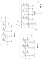
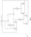
- FIG. 1A shows an example of a switch arrangement 100 that may be used for efficient switching in accordance with one or more aspects described herein.
- the switch arrangement 100 shown in Fig. 1A comprises a first switch Q1, a second switch Q2 and a third switch Q3.
- Switches Q1, Q2 and Q3 are connected in parallel between terminals TA and TB.
- Switches Q1-Q3 are shown as Metal Oxide Semiconductor Field Effect Transistors (MOSFETs), but may also be different types of semiconductor switches, such as Bipolar Junction Transistors (BJTs), Gallium Nitride transistors (GaNs), Silicon Carbide switches (SiCs), Insulated Gate Bipolar Transistors (IGBTs), etc.
- BJTs Bipolar Junction Transistors
- GaNs Gallium Nitride transistors
- SiCs Silicon Carbide switches
- IGBTs Insulated Gate Bipolar Transistors
- terminal TA may be connected to drain terminals of each of switches Q1-Q3, and terminal TB may be connected to source terminals of each of switches Q1-Q3.
- Each of switches Q1-Q3 may feature a gate terminal, denoted G1-G3, respectively, provided for controlling the respective switch: switch Q1 may be controlled via gate terminal G1, switch Q2 may be controlled via gate terminal G2, and switch Q3 may be controlled via gate terminal G3.
- Terminals TA or TB may be used as drain or source terminals for all three switches Q1-Q3. Terminals TA or TB may be mechanically designed to be connected in a power circuit, such as in the same manner that a single switch would have drain or source terminals connected to the power circuit. Each switch may be mechanically attached to a power circuit (e.g., separately). Each switch source or drain terminal may be mechanically designed to be attached to a circuit.
- a controller may be configured to selectively (such as according to a method described herein) apply a voltage (such as via a gate driver, not explicitly depicted in figures herein) to one of gate terminals G1-G3, which may cause the corresponding switch to turn ON.
- the switches may be, by default, in the ON position, in which case the controller may be configured to selectively apply a voltage to one of gate terminals G1-G3, which may cause the corresponding switch to turn OFF.
- Switch module 110B comprises four switches Q1-Q4, which may be packaged and integrated together in a single module housing 105. As shown in this example, various numbers of switches (e.g., other than three) may be used to implement an efficient switching module.
- Switch Q4 may be similar to switches Q1-Q3, but may feature a different electrical parameter (e.g., parasitic capacitance values, conduction resistance [Rds_on], etc.) than one or more of the other switches Q1-Q3.
- Terminals TA or TB may be externally provided (e.g., provided as terminals accessible from outside the module) as power terminals, and/or terminals G1-G4 may be provided externally as control terminals, which may enable an external controller to control switches Q1-Q4.
- Terminals TA or TB may be viewed as common conduction path terminals for switches Q1-Q4, as terminals TA or TB may, for example, conduct current regardless of which switch is ON at any particular time.
- Internal connections between the switches e.g., solder, wires or bus bars connecting the switches in parallel
- Arranging switches Q1 and Q2, or all of Q1-Q3 in an integrated housing, or arranging switches Q1-Q4 in an integrated housing may have the advantage of enabling efficient cooling and packaging of the switches while enabling efficient control and operation of the switches in accordance with one or more aspects described herein.
- a single switch module 110C may include four switches divided into two pairs of switches similar to Q1-Q2 of FIG. 1A , wherein each pair may be connected in parallel.
- a power module may feature two power terminals TA1 and TB1 and two control terminals G1a and G2a for the first switch pair comprising Q1a and Q2a.
- a power module may feature two additional power terminals TA2 and TB2, and two additional control terminals G1b and G2b for the second switch pair comprising Q1b and Q2b.
- Switches Q1a and Q2a may differ from one another in at least one electrical parameter.
- Switches Q1b and Q2b may differ from one another in at least one electrical parameter.
- switch module 110D may include two groups of three switches connected in parallel.
- a first switch group may be comprised of switches Q1a-Q3a connected in parallel
- a second switch group may be comprised of switches Q1b-Q3b connected in parallel.
- the first switch group may be connected between terminals TA and TC.
- the second switch group may be connected between terminals TC and TB.
- a switch module may contain a number of power terminals and may contain a number of control terminals, wherein in some variations, the number of control terminals corresponds to the number of switches.
- a switch module may feature 3 power terminals (TA, TC and TB) and 6 control terminals (one for each switch). While FIG. 1D contains 3 power terminals and 6 control terminals, a single switch module may contain more than 3 power terminals and/or more than 6 control terminals. Additionally or alternatively, while FIG. 1D contains 3 power terminals and 6 control terminals, a single switch module may contain less than 3 power terminals and/or less than 6 control terminals.
- a first trio may be configured to operate in a substantially complementary manner with a second trio.
- a first trio of switches e.g., Q1a-Q3a
- a second trio of switches e.g., Q1b-Q3b
- Each switch in the first trio of switches may be operated to be OFF when the corresponding switch of the second trio of switches is ON.
- each switch in the second trio of switches may be operated to be OFF when the corresponding switch of the first trio of switches is ON.
- the number of control terminals may correspond to the number of switches.
- six control terminals e.g., G1a-G3a and G1b-G3b
- the switch module e.g., as may be shown in Fig. ID
- each control terminal controls a corresponding switch.
- Each complementary switch pair e.g., Q1a, Q1b
- Q1a, Q1b might not be fully complementary.
- Q1a and Q1b may be OFF at the same time (e.g., when a different complementary switch pair is being used).
- both Q1a and Q1b may be ON at the same time (e.g., when it may be desirable to directly connect terminals TA and TC).
- control signals provided for the controlling switches may be provided by analog hardware logic circuits.
- control signals may be generated by digital hardware or software, and may be provided by a digital controller.
- Switch module 110E may include switches Q1a-Q3a and Q1b-Q3b, as arranged in FIG. 1D .
- Voltmeter 120 may measure voltage between terminals TA and TC.
- Voltmeter 122 may measure voltage between terminals TC and TB.
- Ammeter 121 may measure current flowing through terminal TC.
- additional voltmeters and/or ammeters may be used.
- a voltage sensor between terminal TC and a terminal of a different circuit (not shown in FIG. IE) may be used.
- Voltmeters 120 and 122, ammeter 121, and additional voltmeters and/or ammeters may be collectively referred to as "sensors".
- Selector 111 may be integrated in switch module 110E and may receive voltage and current measurements from voltmeter 120, voltmeter 122, ammeter 121, or additional measurement devices.
- Selector 111 may be configured to receive an external control signal (e.g., HS_ON). Based on receiving the HS_ON signal and the current and/or voltage values measured by the sensors, selector 111 may control one or more of the switches (e.g., Q1a-Q3a and Q1b-Q3b) to be ON, and may control the one or more of the remaining switches to be OFF.
- an external control signal e.g., HS_ON
- selector 111 may control one or more of the switches (e.g., Q1a-Q3a and Q1b-Q3b) to be ON, and may control the one or more of the remaining switches to be OFF.
- selector 111 may alternate (e.g., by a PWM switching scheme, such as at a relatively low frequency) the state of two switches (e.g., Q1a and Q1b). Alternating the state of the switches may be characterized by low-conduction-loss performance such that the state of Q1a tracks the external control signal (e.g., the HS_ON signal) and the state of Q1b is always the opposite of the external control signal (e.g., the HS_ON signal). Selector 111 may leave the other switches (e.g., Q2a, Q2b, Q3a, Q3b) OFF.
- a PWM switching scheme such as at a relatively low frequency
- selector 111 may alternate (e.g., by a PWM switching scheme at a relatively high frequency) the state of two switches (e.g., Q3a and Q3b) characterized by low-switching-loss performance and leave the other switches (e.g., Q1a, Q1b, Q2a, Q2b) OFF.
- switches e.g., Q3a and Q3b
- Selector 111 may be a digital controller that may be configured to receive external control signals (e.g., an HS_ON signal) and sensor measurements via input ports, and may be configured to control switches (e.g., Q1a-Q3b) via digital output signals (e.g., as provided by selector 111 to gate drivers connected to the corresponding gate terminals G1a-G3b). Selector 111 may comprise an analog or mixed-signal control circuit.
- external control signals e.g., an HS_ON signal
- sensor measurements e.g., sensor measurements via input ports
- control switches e.g., Q1a-Q3b
- digital output signals e.g., as provided by selector 111 to gate drivers connected to the corresponding gate terminals G1a-G3b.
- Selector 111 may comprise an analog or mixed-signal control circuit.
- selector 111 may be configured to turn one of Q1a, Q2a, and Q3a ON when the HS_ON signal is "high" (e.g., a logical '1' signal is received on a HS_ON input line).
- Selector 111 may be configured to select one or more of Q1a, Q2a and Q3a to turn ON based on current and/or voltage measurements indicating an operating point of switch module 110E.
- selector 111 may be configured to set all of Q1a-Q3a to OFF, and at least one of one of switches Q1b, Q2b and Q3b to ON.
- modules integrating switch arrangements in accordance with one or more aspects described herein may include two or more groups, and that each group may include two or more switches having at least one different electrical parameter.
- each group may include two or more switches having at least one different electrical parameter.
- multiple circuits corresponding to switch arrangements and/or modules 110A-110E may be packaged together as a single module.
- Switch module 140 may include a number of switch modules (e.g., switch modules 110D1, 110D2, and 110D3), each of which may be similar to or may incorporate switch module 110D of FIG. 1D .
- switch module 140 may include two switch modules (e.g., 110D1 and 110D2) that are controlled to implement a full-bridge inverter.
- a first switch module (e.g., 110D1) may be controlled (e.g., via one or more of gate inputs Ga-Gn) to receive a first input voltage between terminals TA1 and TB1, and may output a first output voltage between terminals TC1 and TB1, or between terminals TC1 and TA1.
- a second switch module (e.g., 110D2) may be controlled to receive a second input voltage between terminals TA2 and TB2, and may output a second output voltage between terminals TC2 and TB2, or between terminals TC2 and TA2.
- the second input voltage may be the same as the first input voltage (e.g., terminals TA1 and TB1 may be connected to terminals TA2 and TB2, respectively).
- the second output voltage may be controlled such that a differential voltage between terminals TC1 and TC2 may form a sine wave.
- the firm output voltage at terminal TC1 may form a unipolar sine-wave shape form with respect to terminal TB1, and the second output voltage at terminal TC1 may be similar to the first output voltage, but phase shifted by 180 degrees, to form a bipolar sine wave between terminals TC1 and TC2.
- All three switch modules 110D1-110D3 may be controlled to output three sine wave voltages at 120-degree phases shifts with respect to one another, which may form a three-phase inverter output.
- Switch arrangement 130 may feature a number of switches (e.g., Q1, Q2 and Q3) and may be implemented using different switch types.
- switch Q1 of switch arrangement 130 may be implemented using a MOSFET
- switch Q2 of switch arrangement 130 may be implemented using a Bipolar Junction Transistor (BJT)
- switch Q3 of switch arrangement 130 may be implemented using an Insulated Gate Bipolar Transistor (IGBT).
- IGBT Insulated Gate Bipolar Transistor
- Switch Q1 may be PWM-switched during a first time period corresponding to a time when a sine wave changes rapidly, which may take advantage of superior switching characteristics of a MOSFET.
- Switch Q3 may be PWM-switched during a third time period corresponding to a time when a sine wave changes slowly and may conduct high current, which may take advantage of superior conduction characteristics of an IGBT.
- Switch Q2 may be PWM-switched during a second time period corresponding to a time when a sine wave changes at a medium rate and may conduct a medium current level, which may take advantage of the switching loss - conduction loss balance of the BJT.
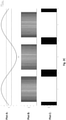
- FIG. 2A shows waveforms that may be measured when operating within switch arrangement 100 of FIG. 1A , in accordance with one or more aspects described herein.
- REF rectified sinusoid reference signal
- a rectified sinusoid reference signal may be used, for example, for operating switches in a two-stage inverter circuit.
- the first stage may comprise a DC/DC converter configured to output a rectified sine wave voltage
- a second stage may comprise a low frequency unfolding bridge configured to convert the rectified sine wave output by the first stage to a bipolar sine wave output.
- a rectified sinusoid reference signal may also be used, for example, for operating switches in a two-stage rectifier circuit.
- the first stage may comprise a low frequency unfolding bridge configured to receive a sine wave input and to output a rectified sine wave (e.g., that can be used as the REF signal or to create a similarly shaped REF signal), and the second stage may comprise a DC/DC converter configured to convert the rectified sine wave voltage to a substantially constant DC voltage.
- a reference signal may be a reference signal created in hardware or software, and may provide an indication, to the controller, of what voltage should be output by a converter including switches (e.g., Q1-Q2). Additionally or alternatively, the REF signal may provide an indication of a desirable duty cycle for a PWM-controlled switch of a converter.
- reference signal REF may be based on a measured value. For example, in a rectifier circuit, REF may correspond to a measured input voltage. REF may indicate to the controller when a switch from switch arrangement 100 should be ON in order to rectify the received input voltage.
- an inverter circuit may be coupled to an AC grid and the REF signal may correspond to a measured grid voltage connected at the inverter output.
- an inverter circuit may operate in off-grid mode (e.g., when not connected to an externally imposed AC voltage) and the REF signal may be based on a stored value (e.g., a value stored in an internal memory device) or on an internal reference signal generator.
- a first threshold may be indicated by a dashed line having a constant value of about 0.333
- a second threshold may be indicated by a dotted line having a constant value of about 0.666, dividing the value range of the reference signal REF into three portions:
- thresholds may divide the REF signal value range into more than three portions. For example, four thresholds may be used to divide the REF signal value range into five portions. The portions need not be equal in size, and the REF signal may be in one portion for a longer period of time than in another portion.
- a switch Q1 (which may be a switch Q1, Q1a, or Q1b as described herein) may be characterized by electrical parameters resulting in low switching losses (e.g., low parasitic capacitance values, such that a reduced amount of energy is needed to charge and discharge the capacitors turning switch turn-on and turn-off), but high conduction losses (e.g., increased Rds_on), a switch Q3 (which may be a switch Q3, Q3a, or Q3b as described herein) may be characterized by electrical parameters resulting in high switching losses (e.g., large parasitic capacitance values), but low conduction losses (e.g., low Rds_on), and a switch Q2 (which may be a switch Q2, Q2a, or Q2b as described herein) may be characterized by electrical parameters resulting in medium switching losses (e.g., medium parasitic capacitance values) and medium conduction losses (e.g., medium Rds_on).
- low switching losses e.g.
- a controller configured to control switches may be configured to operate (e.g., switch between ON and OFF) switch Q1 at a first frequency when the REF signal is below a first threshold (e.g., is changing rapidly), corresponding to a time period between t0 and t1.
- switches Q2 and Q3 may be held OFF by the controller.
- the controller may be configured to operate switch Q3 at a third frequency when the REF signal is above the second threshold (e.g., changing slowly), corresponding to a time period between t2 and t3.
- switches Q2 and Q1 may be held OFF by the controller.
- the controller may be configured to operate switch Q2 at a second frequency when the REF signal is between the first and second thresholds (e.g., changing at a medium rate), corresponding to a time period between t1 and t2.
- the first frequency may be higher than the second frequency, and the second frequency may be higher than the third frequency.
- the controller may operate the first switch at the first frequency, (e.g., a high frequency, which may be 50kHz) to enable fast tracking of the reference signal. This may have the advantage of allowing Q1's superior switching loss characteristics to avoid incurring substantial switching losses.
- the first time period may correspond to a time when the first current flowing through the switching device is low (e.g., during a zero-crossing of an inverter current that substantially tracks an inverter voltage, such as operation at a low displacement factor [also known as cos ⁇ ]) , which may have the advantage of reducing excessive losses caused by Q1's inferior conduction loss properties.
- a third current e.g., high current
- the third current may be greater than the first current.
- conduction losses may be reduced.
- the controller may control switch Q3 at a relatively low switching frequency (e.g., 10kHz or less) to avoid incurring substantial switching losses caused by Q3's inferior switching properties.
- Switch Q2 may be operated in the second time period at, for example, 25kHz, where a second current (e.g., an intermediate current) may flow through the switching device, which may result in a second rate of change of the reference signal REF (e.g., an intermediate rate of change) and may provide a balance between switching losses and conduction losses.
- the second current may be greater than the first current, but may be less than the third current.
- Plot B depicts an example logical signal (e.g., PWM1) applied to a switch (e.g., Q1) when a controller is controlling a number of switches (e.g., Q1-Q3), in accordance with one or more aspects of described herein.
- a PWM signal e.g., PWM1
- PWM1 may be applied to the gate of Q1, which may turn switch Q1 ON when the PWM signal is high (e.g., a logical '1') and may turn switch Q1 OFF when the PWM signal is low (e.g., a logical '0').
- switch Q1 may always be OFF (e.g., the control signal provided by the controller to the gate of switch Q1 may always be low).
- Plot C depicts an example signal applied to a switch (e.g., Q2) when a controller is controlling a number of switches (e.g., Q1-Q3), in accordance with one or more aspects described herein.
- a switch e.g., Q2
- an example logical signal e.g., PWM2
- PWM2 may be applied to a switch (e.g., Q2) when a reference signal REF is above a first threshold and below a second threshold.
- the frequency of PWM2 may be lower than the frequency of PWM1.
- Plot D depicts an example signal applied to a switch (e.g., Q3) when a controller is controlling a number of switches (e.g., Q1-Q3), in accordance with one or more aspects described herein.
- switches Q1 and Q3 may always be OFF.
- switches Q1 and Q3 may always be OFF.
- switches Q2 and Q1 may always be OFF.
- switch Q1 may switch at 24kHz when in PWM mode
- switch Q2 may switch at 12kHz when in PWM mode
- switch Q3 may switch at 6kHz when in PWM mode.
- period TP1 e.g., the time between rising edges of consecutive pulses of Q1
- period TP2 e.g., the time between rising edges of consecutive pulses of Q2
- period TP3 e.g., the time between rising edge of consecutive pulses of Q3
- FIG. 2C shows waveforms that may be measured when operating a switching device similar to or incorporating those shown in FIGS. 1A-1G , in accordance with one or more aspects described herein.
- REF x sin x + 1 2
- This type of reference signal may be used as part of a two-leg rectifier/inverter circuit.
- the first leg may be configured to output (in the inverter case), or receive as input (in the rectifier case), a voltage signal similar to REF(x) as described above.
- the second leg may comprise a half bridge configured to selectively provide a negative bias such that a sine wave is obtained between the two legs.
- First and second thresholds of 0.333 and 0.666, respectively, may divide the reference signal period into three portions:
- a first switch (whose operation is depicted in Plot C), characterized by having low switching losses, may be operated at a first, high frequency.
- a second switch (whose operation is depicted in Plot B), characterized by having low conduction losses, may be operated at a second, low frequency.
- the first switch may be a switch Q1, Q1a, or Q1b as depicted herein, and the second switch may be a switch Q2, Q2a, or Q2b as discussed herein.
- Switch Q3 may be unused, or might not be included in the circuit.
- the second switch may be a switch Q3, Q3a, or Q3b (e.g., switch Q2 may be unused or absent).
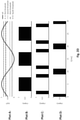
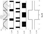
- FIG. 2D shows waveforms that may be measured when operating three switches (e.g., the switching device of FIG. 1A ), in accordance with one or more aspects described herein.
- Plot A displays a reference signal REF oscillating as a positive sinusoid, similar to the REF signal of FIG. 2C .
- Plots B-D show PWM signals used to control the three switches.
- thresholds may be used to determine which switch of a switching device should be used, wherein the value of the first, second, third, and fourth thresholds may be 0.166, 0.333, 0.666, and 0.833, respectively.
- the four thresholds may divide the reference signal period into five portions:
- a first switch optimized for low conduction losses may be switched at a relatively low frequency.
- a third switch optimized for low switching losses may be switched at a relatively high frequency.
- a second switch designed for medium switching losses and medium conduction losses may be switched at an intermediate frequency.
- Carrier wave C1 (indicated by a dashed line) may form a first triangular waveform that oscillates between 0 and 1 at a first frequency of 22kHz.
- Carrier wave C2 (indicated by a dotted line) may form a second triangular waveform that oscillates between 0 and 1 at a second frequency of 14kHz.
- Carrier wave C3 (indicated by a dash-dot line) may form a third triangular waveform that oscillates between 0 and 1 at a third frequency of 5kHz.
- reference signal REF may be compared (e.g., in hardware or software) to carrier wave C1.
- the first switch may be turned ON. Additionally or alternatively, when the value of reference signal REF is less than the value of carrier wave C1, the first switch may be turned OFF.
- reference signal REF may be compared to carrier waves C2 and C3, respectively.
- Method 300 illustrates an example method for operating a number of parallel-connected switches (e.g., Q1-Q3 of FIGS. 1A-1B , or Q1a-Q3a of FIGS. ID-IE).
- Method 300 may be carried out by a controller (e.g., a digital or analog control circuit, a processor, ASIC, etc.) providing control signal to gate drivers configured to drive (e.g., turn ON and OFF) the parallel-connected switches.
- a controller e.g., a digital or analog control circuit, a processor, ASIC, etc.
- gate drivers configured to drive (e.g., turn ON and OFF) the parallel-connected switches.
- the controller may determine a reference voltage value (e.g., V ).
- the controller may determine V by sampling a reference voltage signal.
- the reference voltage signal may be generated internally (e.g., in the controller or in a power device comprising the controller). Additionally or alternatively, the reference voltage signal may be an external reference voltage signal (e.g., V may correspond to an input AC voltage to be rectified by the switches).
- the reference voltage value may be stored in a memory device (internal or external to the controller) and may be part of a sequence of reference values loaded sequentially from memory.
- the controller may compare V to a first threshold (e.g., thresh1 ) . If V is below thresh1, then the controller may determine that switch Q1 is to be operated in PWM mode (e.g., switched between ON and OFF states at a frequency f1 in the kHz or MHz range)., At step 312, after determining that switch Q1 is to be operated in PWM mode, switches Q2-Q3 may be kept OFF. At step 313, V may be compared to a value of a first carrier C1, which may be a triangular wave at a frequency of f1 ) . At step 314, if V is greater than C1, then Q1 may be turned ON.
- a first threshold e.g., thresh1
- step 315 if V is not greater than C1, then Q1 may be turned OFF.
- the controller may loop back to step 310 and may determine a new value of V.
- the controller since the result of step 311 may rarely change compared to the result of step 313 (for example, in the example waveforms of FIGS. 2A-2B , the result of step 311 may change 8 times per second and the result of step 313 may change 24,000 times per second), the controller may repeatedly (e.g. tens, or hundreds of times) skip directly to step 313 (indicated by the dashed line) following step 314 or 315 before returning to step 311.
- step 313 may loop many times to determine whether a new V is greater than C1 without performing step 311 to determine whether Vis greater than thresh1, as it may be expected that it may take many (e.g., hundreds) of loops before V is greater than thresh1.
- the number of consecutive loop iterations e.g., from step 313 to either of steps 314 or 315, to step 310, and then back to step 313) may depend on the value of V and on an estimate of when the result of step 311 may change again.
- step 311 the controller determines that V is greater than tresh1, then the controller may proceed to step 322.
- the controller may compare V to a second threshold (e.g., thresh2 ) to determine if V is less than thresh2.
- a second threshold e.g., thresh2
- the controller may determine that switches Q1 and Q2 may be operated in PWM mode (e.g., switched between ON and OFF states at a frequency f2 in the kHz or MHz range).
- switches Q1 and Q3 may be kept OFF.
- V may be compared to a value of a second carrier C2, which may be a triangular wave at a frequency of f2 .
- C2 may be a triangular wave at a frequency of f2 .
- Q3 may be turned ON. Additionally or alternatively, at step 325, if V is not greater than C2, then Q3 may be turned OFF.
- the controller may loop back to step 310 and may determine a new value of V.
- step 331 the controller may determine that switches Q1 and Q3 may be kept OFF. and may determine that switch Q3 is to be operated in PWM mode according to a third carrier C3 at a third frequency f3 , and may proceed to step 332.
- the controller may compare V to a value of the third carrier C3, which may be a triangular wave at a frequency of f 3, to determine if V is greater than C3.
- step 332 if V is greater than C3, then Q2 may be turned ON. Additionally or alternatively, at step 333, if V is not greater than C3, then Q2 may be turned OFF.
- the controller may loop back to step 310 and determine a new value of V.
- dashed lines have not been drawn between step 310 and steps 324 and 332, but logically, they may exist.
- the controller may skip from step 310 to steps 324 or 332, as described above with respect to step 313, because the result of determining whether V is greater than C2 or C3 may change far more often than the result of whether V is less than thresh2. Similar to the above, the number of "loop skips" may depend on V and on an estimate of when V may be less than thresh2. will change.
- method 300 may be adapted accordingly to account for the additional thresholds.
- the controller may operate Q1 in PWM mode upon detecting that the reference signal is either less than a fourth threshold or greater than a first threshold.
- the controller may operate Q2 in PWM mode upon detecting that the reference signal is either between the first and second thresholds or between the third and fourth thresholds, and so on.
- the controller may compare the change in V to different thresholds. For example, the controller may retain a previous value of V when obtaining a new reference voltage value at step 310, and may calculate a difference between the two values. If the difference is below a first threshold, the controller may operate Q3 in the PWM mode while keeping Q2 and Q1 OFF, since a small difference between consecutive reference values is, according to some embodiments, correlated with large voltage values. If the difference is greater than the first threshold and less than the second threshold, the controller may operate Q2 in the PWM mode while keeping Q3 and Q1 OFF. If the difference is greater than the second threshold, the controller may operate Q1 in the PWM mode while keeping Q3 and Q2 OFF.
- FIG. 4A shows a power converter (depicted here in an exemplary manner as an AC/DC converter, sometimes referred to as a rectifier) including a switching arrangement according to one or more aspects described herein.
- Vac may be an alternating current voltage input to rectifier 400, connected to rectifier input terminals.
- Switches M1-M6 may be arranged such that switches M1-M3 are connected in parallel to form a first parallel switch group.
- Switches M4-M6 may be connected in parallel to form a second parallel switch group.
- the first parallel switch group may be connected in series to the second parallel switch group and may be located between output converter nodes to form a first half bridge.
- Switches M10 and M11 may be connected in series between the output converter nodes to form a second half bridge.
- Inductor L may be connected between a first input terminal and a midpoint node X of the first half bridge.
- a second input terminal may be connected to a midpoint node Y of the second half bridge.
- Capacitor C may be connected across the output terminals, and resistor R may be a load of rectifier circuit connected across the output terminals.
- Controller 410 may be configured to control switches M1-M6 and M10-M11.
- Switch module 110D of FIG. 1D or switch module 110E may be used to implement switches M1-M6 of FIG. 4A .
- Discrete components may be used for a customized switch arrangement.
- Controller 410 may receive input voltage measurements from a voltmeter connected across the input terminals and, based on the input voltage measurements, via control lines 420 (drawn in an incomplete manner, to reduce visual noise), may control switches M1-M6 and M10-M11. Controller 410 may operate switches M1-M6 at relatively high frequencies (e.g., several kHz, tens or hundreds of kHz, even MHz, or GHz, etc.). Controller 410 may operate switches M10-M11 at a line frequency (e.g., 50Hz or 60Hz). During a positive AC frequency half-cycle, controller 410 may keep switch M11 ON and may keep switch M10 OFF, and may keep switches M1-M6 at higher frequencies according to changes in the input voltage during the positive half-cycle.
- controller 410 may keep switch M11 OFF and switch M10 ON, and switches M1-M6 at higher frequencies according to changes in the input voltage during the negative half-cycle.
- This arrangement may provide a benefit of having only two switches (e.g., one from the first half bridge and one from the second half bridge) in a full conduction path during operation of the rectifier, reducing conduction losses, while the second half-bridge is switched at a line frequency, reducing switching losses.
- operating switches M1-M6 at different frequencies, according to a value of a reference voltage signal based on input voltage Vac may further reduce switching and conduction losses, as described above.
- FIG. 4B shows example waveforms that may be measured and/or used in operation of the AC/DC converter of FIG. 4A .
- REF reference signal
- REF t ⁇ sin ⁇ t for ⁇ t ⁇ ⁇ sin ⁇ t + 1 for ⁇ ⁇ ⁇ t ⁇ 2
- REF may be based on the input voltage to converter 400.
- the input voltage may be sensed, and during a negative half-wave of the input voltage (e.g., when the input voltage is negative), a shifted REF sample may be provided to the control method that controls switches M1-M6 and M10-M11 based on the REF sample.
- switches M4-M6 may be switched by the controller based on a magnitude of reference signal REF.
- Switch M4 may be switched when REF is less than a first threshold (e.g., thresh1 ) .
- Switch M5 may be switched when REF is greater than thresh1, but less than a second threshold (e.g., thresh2 ) .
- Switch M6 may be switched when REF is greater than thresh2.
- Switch M1 may be substantially complementary to switch M4 (e.g., when switch M4 is ON, switch M1 is OFF, and vice-versa), switch M2 may be substantially complementary to switch M5, and switch M3 may be substantially complementary to switch M6.
- switch M4 may be implemented using a transistor characterized by having low switching losses.
- switch M6 may be implemented using a transistor having low conduction losses (i.e., a lower ON-resistance compared to switch M4).
- switch M5 may be implemented using a transistor characterized by having higher switching losses than switch M4, lower switching losses than switch M6, higher conduction losses than switch M6, and lower conduction losses than switch M4.
- Switch M11 may be ON during the positive half-wave half-period of the input voltage and switch M10 may be ON during the negative half-wave half-period of the input voltage to provide a rectified DC voltage at the output terminals of converter 400.
- a power converter similar to converter 400 may be operated as a DC-to-AC converter (e.g., an inverter), where a DC voltage input is provided (e.g., by one or more photovoltaic panels, batteries, capacitors, fuel cells, or other DC sources) and an AC voltage is output.
- switches M1-M6 may be operated according to the magnitude of an output voltage of the converter (e.g., reference signal REF may be based on a measured or target output voltage).
- switches may be selected for use in operation in accordance with one or more aspects described herein, according to an expected time of operation in each phase of a reference voltage. For example, in some power electronics design problems, it may be difficult to predict or to estimate how long a power device will be in operation in a particular mode, and this difficulty may pose a challenge in selecting electronics for high-efficiency performance.
- the duration of each time period for operation in a particular mode may be predetermined or pre-estimated, and electronics may be selected according to the predetermined or pre-estimated time periods.
- Plot D of FIG. 2D illustrates one scenario where a first switch may be operated in PWM mode during approximately 25% of each cycle.
- Plot C of FIG. 2D illustrates a scenario where a second switch that may be operated in PWM mode during approximately 27% of each cycle.
- Plot B of FIG. 2D illustrates a scenario where a third switch may be operated in PWM mode during approximately 48% of each cycle.
- a circuit designer may emphasize selection of a high-quality third switch (e.g., a switch having low conduction losses) to improve total efficiency of the switch module.
- the first, second, third, and fourth thresholds of FIG. 2D may be modified such that each of the first, second, and third switches may be operated for substantially equal periods of time to reduce the risk of overheating a single switch.
- changing the first threshold to 0.5 and the second threshold to 0.866 may result in substantially equal time portions for operating switches Q1-Q3 in PWM mode (e.g., if the first threshold is 0.5 and the second threshold is 0.866, then t 1 - t 0 ⁇ t 2 - t 1 ⁇ t 3 - t 2).
- the thresholds may be further adjusted to account for variations in a PWM duty cycle of each switch, to optionally cause each switch to be ON for substantially equal periods of time, to carry a substantially equal average current, and/or to generate substantially equal switching and/or conduction losses, which may all promote heat generation being substantially uniformly generated by the switches.
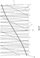
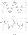
- FIG. 5A shows example current and voltage waveforms that may be present at an output of an inverter operated in accordance with one or more aspects described herein.
- FIG. 5A illustrates a voltage waveform (dashed line) and a current waveform (solid line).
- the voltage waveform may be a sinusoid having an RMS amplitude of 220V and a 50Hz frequency.
- the current waveform may be a sinusoid having an RMS amplitude of 11A and a 50Hz frequency.
- the current waveform and the voltage waveform may be substantially in-phase, corresponding to a phase shift of approximately zero and a 'real power' mode of operation.
- the 'real power' mode of operation may be common when the inverter is connected to a well-balanced and stable electrical grid.
- the grid may apply a "clean” (i.e., not substantially distorted) sine wave voltage at the output of the inverter and may draw a "clean" sine wave output current from the inverter, such that the voltage and current sine wave outputs are substantially in-phase.
- voltage peak 511 and current peak 512 may occur substantially at a common time
- voltage zero-crossing 513 and current zero-crossing 514 may occur substantially at a common time.
- a switch exhibiting low switching losses may be operated at a relatively high frequency during a time segment corresponding to the voltage and current zero-crossings, and a different switch exhibiting low conduction losses (but potentially high switching losses) may be operated at a relatively low frequency during a time segment corresponding to the voltage and current peaks.
- FIG. 5B shows example current and voltage waveforms that may be present at an output of an inverter operated in accordance with one or more aspects described herein.
- FIG. 5B illustrates a voltage waveform (dashed line) and a current waveform (solid line).
- the voltage and current waveforms may be substantially the same as those of FIG. 5A , but may be phase-shifted approximately 45 degrees, corresponding to a 'combined real and reactive power' mode of operation. This mode of operation may occur when, in addition to providing the grid with real power, the inverter may inject reactive power into the grid (e.g., to maintain the grid voltage at a suitable level).
- the inverter may provide a current waveform with a phase shift of 90 degrees compared to the voltage waveform and may inject, into the grid, reactive power, but might not inject active power.
- a controller of an inverter may selectively operate different switches during different time segments along the voltage sine wave.
- the controller may select the different switches to operate during different time segments according to measured current and/or voltage values and calculation, estimation, and/or prediction of losses associated with operating each switch.
- FIG. 5C shows example current and voltage waveforms that may be present at an output of an inverter operated in accordance with one or more aspects described herein.
- FIG. 5C illustrates a voltage waveform (dashed line) and a current waveform (solid line).
- the current waveform may be distorted.
- a distorted current waveform may be caused, for example, by nonlinear loads connected to the inverter output. For example, during a power outage, an inverter may enter a "backup power" mode of operation and may provide power to nonlinear loads present at a location (e.g., in a home).
- an inverter may be mounted within a particular location (e.g., a remote cabin), and may be connected solely to the loads present in the remote cabin and never connected to a large power grid.
- the current waveform of FIG. 5C may feature current peak 505, which may be relatively "sharp” (e.g., featuring a rapid rise and fall compared to a sine wave peak), leading to large current levels for relatively short periods of time and relatively small current levels for greater periods of time.
- Current peak 505 may occur at a time very close to the voltage zero-crossing, which may lead to a possible tradeoff between switch losses and conduction losses.
- Fig. 6A illustrates an example method for operating a power converter (e.g., an inverter) in accordance with one or more aspects described herein.
- a power converter e.g., an inverter
- the processes illustrated in FIG. 6A are merely sample processes and functions.
- Method 600 may be applicable to any of the embodiments disclosed herein, and may be particularly beneficial with respect to operating a power converter in the presence of voltage and current that are distorted (e.g., not "clean" sine waves) and/or phase shifted with respect to one another.
- a controller may be configured to execute method 600 (e.g., a controller may be configured to operate one or more of the switches and/or switch modules disclosed herein). For example, the controller may be configured to operate the switches shown in FIGS. 1A-1G , controller 410 of FIG. 4A , and/or switches of an inverter configured to output the voltage and/or current waveforms of FIGS. 6A-6C ).
- the controller may select a default mode of operation (e.g., operate a particular switch of a plurality of parallel-connected switches or operate various switches according to a voltage waveform and without considering current measurements, as described in example method 300 of FIG. 3 , and the like).
- the controller may monitor current and/or voltage at an input and/or an output of a power converter comprising the switches and/or switch modules (e.g., the controller may measure current and/or voltage inputs and/or outputs over time and may log the measurements).
- the controller may calculate periodic parameters related to the voltage and/or current monitored at the step 610.
- the periodic parameters may include, for example, frequency, amplitude and/or phase of the current and/or voltage.
- the controller may identify (e.g., by performing calculations based on values obtained during the monitoring) one or more of a current peak, a current zero-crossing, a voltage peak, or a voltage zero-crossing.
- the controller may calculate the timing of the current peak during a cycle, the phase shift between the current peak and the voltage peak and/or the voltage zero-crossing, and/or the phase shift between the voltage peak and the current zero-crossing.
- the controller may calculate derivatives (e.g., a rate of change) of the voltage and/or the current at various points within the period.
- the controller may calculate estimated and/or predicted losses based on the periodic parameters calculated at step 611. For example, the controller may calculate expected losses associated with one or more different switching schemes. The controller may select a particular switching scheme based on that particular switching scheme having lower expected losses compared to another scheme. For example, the controller may determine that utilizing a single switch/switch-pair of a plurality of switches/switch-pairs (e.g. using only switch Q1 of FIGS. 1A and 1B or utilizing only switch pair Q1a and Q1b of FIG. ID) may cause an estimated 10W of combined conduction and switching losses per cycle.
- a single switch/switch-pair of a plurality of switches/switch-pairs e.g. using only switch Q1 of FIGS. 1A and 1B or utilizing only switch pair Q1a and Q1b of FIG. ID
- the controller may determine that utilizing two or more switches/switch-pairs at different times (e.g., using all of switches Q1-Q3 of FIGS. 1A and 1B or using all of the switch pairs of FIG. ID) may cause an estimated 4W of combined conduction and switching losses per cycle.
- the controller may select to utilize the switches causing the lower losses and, at step 613, may operate the switches according to the selected switching scheme.
- the controller may continue to monitor the voltage and current waveforms over time to detect changes to the voltage and/or current signals and to adapt the switching scheme accordingly. However, it may be inefficient to implement all of the steps of method 600 constantly and for all time. Therefore, the controller may implement two control loops.
- a first loop e.g., the fast loop
- continuously switching between steps 610 and 613 may cause the controller to continuously operate the switches according to the selected switching scheme while continuously monitoring the voltage and current processes by the converter.
- a second loop (e.g., the slow loop), indicated by the solid lines, may cause the controller to periodically (e.g., every second, several seconds, tens of seconds, or minutes) re-calculate periodic parameters and determine a reduced-losses switching scheme.
- Method 601 may be used as step 612 in method 600 of FIG. 6A , and may be executed by a controller similar to or incorporating the controller executing method 600. In some variations, for example to reduce a computational load on the controller executing method 600, a separate controller may be used.
- the controller may identify a time period used for loss-analysis.
- the time period may be obtained as a result of calculations performed at step 611 of method 600. Additionally or alternatively, the controller may identify the time period using input from a user (e.g., a configuration parameter input via a graphical user interface). Additionally or alternatively, the time period may be hard-coded (e.g., for an inverter configured to output a 50Hz voltage waveform, the time period may be hard-coded as being 20ms).
- the controller may divide the time period into a number of segments for separate analysis (e.g., the time period may be divided into N segments, wherein N may be2, 3, 4, 10, 100, or even more).
- the controller may evaluate whether all segments have been evaluated or analyzed. If the controller determines that there is at least one segment that has not been evaluated, then the controller may proceed to step 620. At step 620, the controller may select a segment that has not been evaluated.
- the controller may calculate the current and voltage parameters associated with the segment identified in step 620.
- the parameters may include amplitudes, phases, rates of change (ROC) of the voltage and/or current within the segment, and the like.
- the controller may base its calculations on measured current and voltage values. Additionally or alternatively, in some embodiments, the controller may base its calculations on predicted and/or estimated values.
- the controller may calculate segment losses according to one or more switching schemes within the segment.
- the losses may correspond to measured losses.
- the controller may calculate measured losses by multiplying the measured current and voltage values at the input and output of a power converter, and subtracting the output power from the input power to obtain losses. Additionally or alternatively, the losses may correspond to predicted losses.
- the controller may calculate predicted losses by squaring a measured current and multiplying the squared current with several potential Rds_on values, wherein each Rds_on value may correspond to a different switch.
- the controller may calculate predicted losses by calculating, based on a measured voltage, switching loss across one or more switches being switched under the measured voltage and determining how many times the switches may need to be switched in order to meet the requisite voltage rate-of-change within the segment.
- the controller may select a switch for utilization in the segment under analysis, and may select a switching frequency for use within the segment. For example, the controller may determine that a certain segment incurred average losses of 3W when utilizing a first switch, that the losses were predominantly due to conduction losses, and that the segment could have incurred average losses of 2W if a different switch (e.g., having a smaller Rds_on) were used. The controller may determine that a third switch, having an even larger Rds_on, would incur losses of 6W, and may, therefore, be less suitable.
- the controller may balance conduction loss considerations with switching loss and/or ROC considerations. For example, the controller may determine that a first switch may provide lower conduction losses, but might not meet the required voltage ROC unless it were switched at a high frequency that would cause increased switching losses. The controller may select a switch and a switching frequency for operating the switch such that total losses may be reduced and the resultant waveforms may be satisfactory (e.g., conforming to harmonic distortion requirements and the like).
- the controller may select a segment switching frequency for the switch to reduce losses as much as possible.
- the controller may select a lower frequency for segment switching as a lower frequency may result in fewer losses.
- the controller may select a segment switching frequency that may maintain a required ROC. However, lower frequency segment switching may make it difficult for the controller to maintain a high ROC.
- the controller may select a segment switch in order to reduce combined switching and conduction losses as much as possible. The controller may save the switch and/or selected frequency to memory, and may return to step 619.
- the controller may proceed to step 624.
- the controller may provide the collection of segments, switches, and frequencies to a controller (which may be the same controller) or other mechanism configured to operate the switches at the selected frequencies.
- a controller may be configured to operate a first switch for incurring preferred (e.g., lower) switching loss, and a second switch for reducing conductance losses.
- a first switch having low switching losses may be used for transitioning between ON and OFF states, and a second switch having a low Rds_on may be switched to the same state as the first switch to obtain lower conductance losses.
- switch Q1 may be used to "hard switch” between ON and OFF states, and switch Q3 may "follow" switch Q1 (e.g., turn ON right after Q1) in order to reduce conduction losses.
- switch Q1 may be used to "hard switch” between ON and OFF states
- switch Q3 may "follow" switch Q1 (e.g., turn ON right after Q1) in order to reduce conduction losses.
- the same technique may be applied to the switch arrangements for FIGS. 1A-1G and 4A .
- a controller may, instead of or in addition to monitoring current and/or voltage values, predict future current and/or voltage values, and may determine a switching scheme according to the predicted values.
- an inverter may be configured to output a voltage signal according to a sequence of reference values loaded sequentially from memory.
- the inverter may predict a voltage value at a future time and may select a switch for operation during one or more time portions of a period based on the predicted voltage.
- the controller may predict and/or estimate current at a future time.
- the controller may predict and/or estimate future losses according to the predicted and/or estimated voltage and/or current.
- the controller may select a switch for operation during one or more time portions of a period based on the predicted and/or estimated future losses.
Applications Claiming Priority (1)
| Application Number | Priority Date | Filing Date | Title |
|---|---|---|---|
| US202063060312P | 2020-08-03 | 2020-08-03 |
Publications (1)
| Publication Number | Publication Date |
|---|---|
| EP3952084A1 true EP3952084A1 (de) | 2022-02-09 |
Family
ID=77206957
Family Applications (1)
| Application Number | Title | Priority Date | Filing Date |
|---|---|---|---|
| EP21189344.1A Pending EP3952084A1 (de) | 2020-08-03 | 2021-08-03 | Verfahren und vorrichtung zur effizienten umschaltung |
Country Status (3)
| Country | Link |
|---|---|
| US (2) | US11677307B2 (de) |
| EP (1) | EP3952084A1 (de) |
| CN (1) | CN114070022A (de) |
Families Citing this family (1)
| Publication number | Priority date | Publication date | Assignee | Title |
|---|---|---|---|---|
| CN115848200B (zh) * | 2023-02-06 | 2023-05-16 | 石家庄科林电气股份有限公司 | 群控充电系统及其控制方法 |
Citations (6)
| Publication number | Priority date | Publication date | Assignee | Title |
|---|---|---|---|---|
| US20060267542A1 (en) * | 2005-05-27 | 2006-11-30 | Lixiang Wei | Pulse width modulation (PWM) rectifier with variable switching frequency |
| US20080030176A1 (en) * | 2002-07-10 | 2008-02-07 | Sehat Sutardja | Power array system and method |
| US20170331362A1 (en) * | 2014-11-26 | 2017-11-16 | Robert Bosch Gmbh | Method and Device for Controlling Power Semiconductor Switches Connected in Parallel |
| EP3518400A1 (de) * | 2018-01-25 | 2019-07-31 | Toyota Jidosha Kabushiki Kaisha | Stromwandlungsvorrichtung |
| CN110707906A (zh) * | 2019-10-11 | 2020-01-17 | 湖南大学 | 一种基于Si/SiC混合开关的逆变器窄脉冲消除方法 |
| US20200220449A1 (en) * | 2019-01-08 | 2020-07-09 | Toyota Jidosha Kabushiki Kaisha | Power converter |
Family Cites Families (10)
| Publication number | Priority date | Publication date | Assignee | Title |
|---|---|---|---|---|
| US20130279228A1 (en) * | 2012-04-23 | 2013-10-24 | General Electric Company | System and method for improving low-load efficiency of high power converters |
| US20150171770A1 (en) * | 2012-04-24 | 2015-06-18 | General Electric Company | Differential gate resistor design for switching modules in power converter |
| US9397657B1 (en) * | 2014-07-24 | 2016-07-19 | Eaton Corporation | Methods and systems for operating hybrid power devices using multiple current-dependent switching patterns |
| US9722581B2 (en) * | 2014-07-24 | 2017-08-01 | Eaton Corporation | Methods and systems for operating hybrid power devices using driver circuits that perform indirect instantaneous load current sensing |
| CN106208769B (zh) * | 2014-10-09 | 2020-02-07 | 松下知识产权经营株式会社 | 电力转换装置 |
| WO2017037942A1 (ja) * | 2015-09-04 | 2017-03-09 | 三菱電機株式会社 | 電動機駆動装置および空気調和機 |
| US10291110B2 (en) * | 2016-04-19 | 2019-05-14 | Denso Corporation | Driving circuit for switching element and power conversion system |
| US10245961B2 (en) * | 2016-06-01 | 2019-04-02 | Current Ways, Inc. | Inverter-charger combination |
| JP6724706B2 (ja) * | 2016-10-11 | 2020-07-15 | 株式会社デンソー | スイッチング素子の駆動回路 |
| JP7000968B2 (ja) * | 2018-04-05 | 2022-01-19 | 株式会社デンソー | スイッチの駆動回路 |
-
2021
- 2021-08-03 CN CN202110888714.0A patent/CN114070022A/zh active Pending
- 2021-08-03 US US17/393,091 patent/US11677307B2/en active Active
- 2021-08-03 EP EP21189344.1A patent/EP3952084A1/de active Pending
-
2023
- 2023-04-24 US US18/305,819 patent/US20230387785A1/en active Pending
Patent Citations (6)
| Publication number | Priority date | Publication date | Assignee | Title |
|---|---|---|---|---|
| US20080030176A1 (en) * | 2002-07-10 | 2008-02-07 | Sehat Sutardja | Power array system and method |
| US20060267542A1 (en) * | 2005-05-27 | 2006-11-30 | Lixiang Wei | Pulse width modulation (PWM) rectifier with variable switching frequency |
| US20170331362A1 (en) * | 2014-11-26 | 2017-11-16 | Robert Bosch Gmbh | Method and Device for Controlling Power Semiconductor Switches Connected in Parallel |
| EP3518400A1 (de) * | 2018-01-25 | 2019-07-31 | Toyota Jidosha Kabushiki Kaisha | Stromwandlungsvorrichtung |
| US20200220449A1 (en) * | 2019-01-08 | 2020-07-09 | Toyota Jidosha Kabushiki Kaisha | Power converter |
| CN110707906A (zh) * | 2019-10-11 | 2020-01-17 | 湖南大学 | 一种基于Si/SiC混合开关的逆变器窄脉冲消除方法 |
Non-Patent Citations (1)
| Title |
|---|
| WANG YE ET AL: "Efficiency Improvement of Grid Inverters With Hybrid Devices", IEEE TRANSACTIONS ON POWER ELECTRONICS, INSTITUTE OF ELECTRICAL AND ELECTRONICS ENGINEERS, USA, vol. 34, no. 8, 1 August 2019 (2019-08-01), pages 7558 - 7572, XP011727065, ISSN: 0885-8993, [retrieved on 20190523], DOI: 10.1109/TPEL.2018.2881115 * |
Also Published As
| Publication number | Publication date |
|---|---|
| CN114070022A (zh) | 2022-02-18 |
| US20230387785A1 (en) | 2023-11-30 |
| US20220037986A1 (en) | 2022-02-03 |
| US11677307B2 (en) | 2023-06-13 |
Similar Documents
| Publication | Publication Date | Title |
|---|---|---|
| Barater et al. | Performance evaluation of a three-level ANPC photovoltaic grid-connected inverter with 650-V SiC devices and optimized PWM | |
| Iman-Eini et al. | A modular strategy for control and voltage balancing of cascaded H-bridge rectifiers | |
| Onederra et al. | Three-phase VSI optimal switching loss reduction using variable switching frequency | |
| KR101297453B1 (ko) | 모터 제어 장치 및 공기 조화기 | |
| CN107567680B (zh) | 具有有源转换器的变速驱动器 | |
| EP2472708B1 (de) | Stromumwandlungsvorrichtung und steuerungsverfahren dafür | |
| Han et al. | Analysis of a SiC three-phase voltage source inverter under various current and power factor operations | |
| Ho et al. | Practical implementation of an interleaved boost converter using SiC diodes for PV applications | |
| Li et al. | An SiC MOSFET and Si diode hybrid three-phase high-power three-level rectifier | |
| Friedli et al. | A semiconductor area based assessment of ac motor drive converter topologies | |
| US20230387785A1 (en) | Method and Apparatus for Efficient Switching | |
| Cavalcanti et al. | Efficiency evaluation in grid connected photovoltaic energy conversion systems | |
| Ortmann et al. | High switches utilization single-phase PWM boost-type PFC rectifier topologies multiplying the switching frequency | |
| Sanjeev et al. | Analysis of conduction and switching losses in two level inverter for low power applications | |
| Song et al. | Elimination of abnormal output voltage in a hybrid active NPC inverter | |
| Gutierrez et al. | Cost-effective matrix rectifier operating with hybrid bidirectional switch configuration based on Si IGBTs and SiC MOSFETs | |
| Pathak et al. | 3-Phase Power Factor Correction using Vienna rectifier approach and modular construction for improved overall performance, efficiency and reliability | |
| Papastergiou et al. | Comparison of losses in multilevel converters for aerospace applications | |
| KR100902940B1 (ko) | 단상 더블 컨버젼 방식을 갖는 무정전 전원장치의 스위칭 제어 시스템 | |
| Ye et al. | Efficiency comparison for microturbine power conditioning systems | |
| Heerdt et al. | Semiconductors current efforts and losses evaluation for single-phase three-level regenerative PWM rectifiers | |
| Tang et al. | A design investigation of A 1 MVA SiC medium voltage three phase rectifier based on isolated dual active bridge | |
| Xia et al. | Investigation of Hybrid Three-Level Hybrid Device (Hybrid 2) Active Neutral-Point-Clamped Converter | |
| Jamal et al. | Variable switching frequency algorithm for optimal tradeoff between switching losses and total demand distortion in grid-tied three-phase voltage-source inverters | |
| Xu et al. | A Model for Inverter Loss Considering Output Current Ripple |
Legal Events
| Date | Code | Title | Description |
|---|---|---|---|
| PUAI | Public reference made under article 153(3) epc to a published international application that has entered the european phase |
Free format text: ORIGINAL CODE: 0009012 |
|
| STAA | Information on the status of an ep patent application or granted ep patent |
Free format text: STATUS: THE APPLICATION HAS BEEN PUBLISHED |
|
| AK | Designated contracting states |
Kind code of ref document: A1 Designated state(s): AL AT BE BG CH CY CZ DE DK EE ES FI FR GB GR HR HU IE IS IT LI LT LU LV MC MK MT NL NO PL PT RO RS SE SI SK SM TR |
|
| STAA | Information on the status of an ep patent application or granted ep patent |
Free format text: STATUS: REQUEST FOR EXAMINATION WAS MADE |
|
| 17P | Request for examination filed |
Effective date: 20220809 |
|
| RBV | Designated contracting states (corrected) |
Designated state(s): AL AT BE BG CH CY CZ DE DK EE ES FI FR GB GR HR HU IE IS IT LI LT LU LV MC MK MT NL NO PL PT RO RS SE SI SK SM TR |
|
| P01 | Opt-out of the competence of the unified patent court (upc) registered |
Effective date: 20230505 |
|
| STAA | Information on the status of an ep patent application or granted ep patent |
Free format text: STATUS: EXAMINATION IS IN PROGRESS |
|
| 17Q | First examination report despatched |
Effective date: 20231205 |