EP3951873A1 - Ferroelectric material-based three-dimensional flash memory, and manufacture therefor - Google Patents
Ferroelectric material-based three-dimensional flash memory, and manufacture therefor Download PDFInfo
- Publication number
- EP3951873A1 EP3951873A1 EP19923541.7A EP19923541A EP3951873A1 EP 3951873 A1 EP3951873 A1 EP 3951873A1 EP 19923541 A EP19923541 A EP 19923541A EP 3951873 A1 EP3951873 A1 EP 3951873A1
- Authority
- EP
- European Patent Office
- Prior art keywords
- flash memory
- dimensional flash
- layer
- channel layer
- ferroelectric layer
- Prior art date
- Legal status (The legal status is an assumption and is not a legal conclusion. Google has not performed a legal analysis and makes no representation as to the accuracy of the status listed.)
- Pending
Links
Images




Classifications
-
- H—ELECTRICITY
- H10—SEMICONDUCTOR DEVICES; ELECTRIC SOLID-STATE DEVICES NOT OTHERWISE PROVIDED FOR
- H10B—ELECTRONIC MEMORY DEVICES
- H10B51/00—Ferroelectric RAM [FeRAM] devices comprising ferroelectric memory transistors
- H10B51/20—Ferroelectric RAM [FeRAM] devices comprising ferroelectric memory transistors characterised by the three-dimensional [3D] arrangements, e.g. with cells on different height levels
-
- G—PHYSICS
- G11—INFORMATION STORAGE
- G11C—STATIC STORES
- G11C11/00—Digital stores characterised by the use of particular electric or magnetic storage elements; Storage elements therefor
- G11C11/21—Digital stores characterised by the use of particular electric or magnetic storage elements; Storage elements therefor using electric elements
- G11C11/22—Digital stores characterised by the use of particular electric or magnetic storage elements; Storage elements therefor using electric elements using ferroelectric elements
- G11C11/223—Digital stores characterised by the use of particular electric or magnetic storage elements; Storage elements therefor using electric elements using ferroelectric elements using MOS with ferroelectric gate insulating film
-
- G—PHYSICS
- G11—INFORMATION STORAGE
- G11C—STATIC STORES
- G11C11/00—Digital stores characterised by the use of particular electric or magnetic storage elements; Storage elements therefor
- G11C11/21—Digital stores characterised by the use of particular electric or magnetic storage elements; Storage elements therefor using electric elements
- G11C11/22—Digital stores characterised by the use of particular electric or magnetic storage elements; Storage elements therefor using electric elements using ferroelectric elements
- G11C11/225—Auxiliary circuits
- G11C11/2259—Cell access
-
- G—PHYSICS
- G11—INFORMATION STORAGE
- G11C—STATIC STORES
- G11C11/00—Digital stores characterised by the use of particular electric or magnetic storage elements; Storage elements therefor
- G11C11/21—Digital stores characterised by the use of particular electric or magnetic storage elements; Storage elements therefor using electric elements
- G11C11/22—Digital stores characterised by the use of particular electric or magnetic storage elements; Storage elements therefor using electric elements using ferroelectric elements
- G11C11/225—Auxiliary circuits
- G11C11/2275—Writing or programming circuits or methods
-
- G—PHYSICS
- G11—INFORMATION STORAGE
- G11C—STATIC STORES
- G11C11/00—Digital stores characterised by the use of particular electric or magnetic storage elements; Storage elements therefor
- G11C11/56—Digital stores characterised by the use of particular electric or magnetic storage elements; Storage elements therefor using storage elements with more than two stable states represented by steps, e.g. of voltage, current, phase, frequency
- G11C11/5657—Digital stores characterised by the use of particular electric or magnetic storage elements; Storage elements therefor using storage elements with more than two stable states represented by steps, e.g. of voltage, current, phase, frequency using ferroelectric storage elements
-
- H—ELECTRICITY
- H10—SEMICONDUCTOR DEVICES; ELECTRIC SOLID-STATE DEVICES NOT OTHERWISE PROVIDED FOR
- H10B—ELECTRONIC MEMORY DEVICES
- H10B51/00—Ferroelectric RAM [FeRAM] devices comprising ferroelectric memory transistors
- H10B51/30—Ferroelectric RAM [FeRAM] devices comprising ferroelectric memory transistors characterised by the memory core region
-
- H—ELECTRICITY
- H10—SEMICONDUCTOR DEVICES; ELECTRIC SOLID-STATE DEVICES NOT OTHERWISE PROVIDED FOR
- H10D—INORGANIC ELECTRIC SEMICONDUCTOR DEVICES
- H10D64/00—Electrodes of devices having potential barriers
- H10D64/60—Electrodes characterised by their materials
- H10D64/66—Electrodes having a conductor capacitively coupled to a semiconductor by an insulator, e.g. MIS electrodes
- H10D64/68—Electrodes having a conductor capacitively coupled to a semiconductor by an insulator, e.g. MIS electrodes characterised by the insulator, e.g. by the gate insulator
- H10D64/689—Electrodes having a conductor capacitively coupled to a semiconductor by an insulator, e.g. MIS electrodes characterised by the insulator, e.g. by the gate insulator having ferroelectric layers
Definitions
- Bit lines are arranged two-dimensionally, and a plurality of cell strings CSTR are connected in parallel with each of the bit lines.
- the cell strings CSTR may be connected in common with the common source line CSL. That is, a plurality of cell strings CSTR may be disposed between a plurality of bit lines and one common source line CSL.
- the common source line CSL may include a plurality of common source lines, and the plurality of common source lines CSL may be two-dimensionally arranged.
- the same voltage may be electrically applied to the plurality of common source lines CSL, or the plurality of common source lines CSL may be electrically controlled independently of each other.
- the lowest horizontal structure 250a being in contact with the epitaxial patterns 222 may correspond to the ground selection line GSL of the array in the three-dimensional flash memory described with reference to FIG. 1 , and the remaining horizontal structures 250 being in contact with the vertical structures 230 may correspond to the plurality of word lines WL0 to WL3, respectively.
- the existing three-dimensional flash memory with the above structure have difficulty of the scaling in a horizontal direction because the ONO layer included in the vertical structure 230 is 40 nm thick, and requires a high operation voltage of 20 V due to an F-N (Fowler-Nordheim) tunneling operation according to a characteristic of a charge trap flash (CTF) using the ONO layer.
- F-N Finler-Nordheim
- the at least one channel layer 310 may be formed of a semiconductor material including Zn, In, Ga, a Group 4 semiconductor material, or a Group 3-5 compound having a C-axis aligned crystal (CAAC) crystal structure. As such, a cell current may increase, a leakage current may decrease, and a temperature-resistant reliability characteristic may be improved.
- the at least one channel layer 310 may be formed of a ZnO x -based material including at least one of AZO, ZTO, IZO, ITO, IGZO, and Ag-ZnO.
- the at least one channel layer 310 is not limited thereto, and may be formed of single crystal silicon or poly-silicon like a conventional channel layer.
- a drain line (not illustrated) may be connected on the at least one channel layer 310.
- the plurality of electrode layers 330 are stacked to be vertically connected to the at least one ferroelectric layer 320 and are extended and formed in another direction (e.g., the y-axis direction in FIG. 2 ) perpendicular to the one direction.
- a conductive material such as tungsten, titanium, or tantalum may be used as a material for forming the plurality of electrode layers 330.
- a three-dimensional flash memory manufactured by the three-dimensional flash memory manufacturing method includes the structure described above. Also, below, an automated and mechanized manufacturing system may be used as the subject performing the three-dimensional flash memory manufacturing method.
- the manufacturing system extends and forms at least one ferroelectric layer (the at least one ferroelectric layer including a vertical hole therein), which is used as data storage, in the at least one string hole.
- the manufacturing system may form at least one ferroelectric layer using a ferroelectric material of HfO 2 having an orthorhombic crystal structure.
- the manufacturing system may form at least one ferroelectric layer using a ferroelectric material of HfO 2 doped with at least one of Al, Zr, and Si.
- the manufacturing system may adjust a thickness of the at least one ferroelectric layer or may selectively determine a ferroelectric material for forming the at least one ferroelectric layer.
- the manufacturing system may form at least one ferroelectric layer with a ferroelectric material of HfO 2 doped with at least one of Zr and Si to have a high polarization voltage.
- step S610 the manufacturing system prepares, on a substrate, a mold structure in which a plurality of interlayer insulating layers and a plurality of sacrificial layers are stacked alternately.
- step S620 the manufacturing system extends and forms at least one string hole, which penetrates the mold structure to expose the substrate, in one direction.
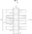
- FIG. 7 is a cross-sectional view illustrating a three-dimensional flash memory according to an embodiment
- FIGS. 8 and 9 are diagrams for describing a multi-level of a three-dimensional flash memory according to an embodiment.
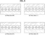
- FIG. 8 is a diagram for describing how a polarization charge amount of at least one ferroelectric layer changes, in a three-dimensional flash memory according to an embodiment
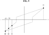
- FIG. 9 is a diagram for describing each operation voltage when a three-dimensional flash memory according to an embodiment implements a multi-level.
- the at least one ferroelectric layer 730 is implemented with a single thin layer of 20 nm or less by using a ferroelectric material, a thickness of the at least one ferroelectric layer 720 may be markedly thin compared to the existing ONO layer. Accordingly, a low operation voltage may be used compared to a three-dimensional flash memory using the existing ONO layer, and the degree of integration in the horizontal direction may be improved.
- the at least one ferroelectric layer 730 may be formed of a plurality of thin layers, as well as a single thin layer. In this case, a total thickness of the plurality of thin layers may be maintained at 20 nm or less.
- the three-dimensional flash memory 700 may change a polarization charge amount of the target memory cell 733 so as to correspond to a first program state by controlling the number of polarized atoms or a polarization rotation angle in the target memory cell 733 like case (a), may change a polarization charge amount of the target memory cell 733 so as to correspond to a second program state by controlling the number of polarized atoms or a polarization rotation angle in the target memory cell 733 like case (c), may change a polarization charge amount of the target memory cell 733 so as to correspond to a third program state by controlling the number of polarized atoms or a polarization rotation angle in the target memory cell 733 like case (d), and may change a polarization charge amount of the target memory cell 733 so as to correspond to an erase state by controlling the number of polarized atoms or a polarization rotation angle in the target memory cell 733 like case (b).
- the three-dimensional flash memory 700 may apply a second program voltage of a negative value (e.g., - 9 V) to the target memory cell 733 such that the number of polarized atoms or a polarization rotation angle in the target memory cell 733 is controlled as illustrated in case (c) of FIG. 8 , that is, may program binary data of "01" by changing a polarization charge amount of the target memory cell 733 so as to correspond to the second program state, and may apply a third program voltage of a negative value (e.g., -8 V) to the target memory cell 733 such that the number of polarized atoms or a polarization rotation angle in the target memory cell 733 is controlled as illustrated in case (d) of FIG. 8 , that is, may program binary data of "10" by changing a polarization charge amount of the target memory cell 733 so as to correspond to the third program state.
- a negative value e.g., - 9 V
- a range between a negative value and a positive value, in which a program voltage to be applied to the target memory cell 733 is adjusted may be determined based on a thickness of the at least one ferroelectric layer 730 and a breakdown voltage of the at least one ferroelectric layer 730.
- the range between a negative value and a positive value, in which a program voltage to be applied to the target memory cell 733 is adjusted may be determined based on a margin of a breakdown voltage according to a thickness of the at least one ferroelectric layer 730. For example, in the case where a thickness of the at least one ferroelectric layer 730 is 20 nm, a margin of a breakdown voltage of the at least one ferroelectric layer 730 may be about 16 V.
- the range between a negative value and a positive value, in which a program voltage to be applied to the target memory cell 733 is adjusted may be determined as a range from -14 V to 10 V.
- a margin of a breakdown voltage of the at least one ferroelectric layer 730 may be about 12V.
- the range between a negative value and a positive value, in which a program voltage to be applied to the target memory cell 733 is adjusted may be determined as a range from -12 V to 10 V.
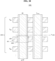
- FIGS. 10 and 11 are cross-sectional views for describing a program operation of a three-dimensional flash memory according to an embodiment.
- case (c) and case (d) of FIG. 8 because a program voltage of a negative value is applied, the same manner may be used except that only a value of a voltage to be applied to the electrode layer 1111 is changed (e.g., in case (c), 9 V is applied to the channel layer of the string or to the channel layer from the substrate corresponding to the string; in case (d), 8 V is applied to the channel layer of the string or to the channel layer from the substrate corresponding to the string).
- case (b) because a program voltage of a positive value is applied, an erase operation to be described with reference to FIG. 12 below may be utilized.
- a three-dimensional flash memory 1200 may perform an erase operation on a plurality of memory cells included in the three-dimensional flash memory 1200 by applying an erase voltage (e.g., 10 V) to each of a plurality of electrode layers 1210 and applying a voltage of 0 V to a channel layer of each string or a channel layer from the substrate corresponding to the string.
- an erase voltage e.g. 10 V
- a polarization charge amount that is determined after the erase operation may be used as one state for a multi-level of a target memory cell 1220. That is, in the three-dimensional flash memory 1200, because an erase state of the target memory cell 1220 indicates one (e.g., "11") of binary data, an erase voltage of 10 V being a positive value to be applied to the target memory cell 1220 in the erase operation (i.e., an erase voltage of 10 V being a positive value to be applied to each of the plurality of electrode layers 1210) may be referred to as a "program voltage" of a positive value for programming binary data of "11".
Landscapes
- Engineering & Computer Science (AREA)
- Computer Hardware Design (AREA)
- Semiconductor Memories (AREA)
- Non-Volatile Memory (AREA)
Abstract
Description
- Embodiments relate to a three-dimensional flash memory, and more particularly, relate to a three-dimensional flash memory capable of improving the degree of integration in a horizontal direction and a manufacturing method thereof.
- A flash memory device that is an electrically erasable programmable read only memory (EEPROM) may be used in common, for example, in a computer, a digital camera, an MP3 player, a game system, a memory stick, etc. The flash memory device electrically programs/erases data by using the F-N (Fowler-Nordheim) tunneling or the hot electron injection.
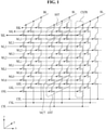
- In detail, referring to
FIG. 1 showing an array of a conventional three-dimensional flash memory, the array of the three-dimensional flash memory may include a common source line CSL, a bit line BL, and a plurality of cell strings CSTR interposed between the common source line CSL and the bit line BL. - Bit lines are arranged two-dimensionally, and a plurality of cell strings CSTR are connected in parallel with each of the bit lines. The cell strings CSTR may be connected in common with the common source line CSL. That is, a plurality of cell strings CSTR may be disposed between a plurality of bit lines and one common source line CSL. In this case, the common source line CSL may include a plurality of common source lines, and the plurality of common source lines CSL may be two-dimensionally arranged. Here, the same voltage may be electrically applied to the plurality of common source lines CSL, or the plurality of common source lines CSL may be electrically controlled independently of each other.
- Each of the cell strings CSTR may include a ground selection transistor GST connected with the common source line CSL, a string selection transistor SST connected with the bit line BL, and a plurality of memory cell transistors MCT interposed between the ground selection transistor GST and the string selection transistor SST. In each cell string CSTR, the ground selection transistor GST, the string selection transistor SST, and the memory cell transistors MCT may be connected in series.
- The common source line CSL may be connected in common sources of the ground selection transistors GST. In addition, a ground selection line GSL, a plurality of word lines WL0 to WL3, and a plurality of string selection lines SSL, which are disposed between the common source line CSL and the bit line BL, may be respectively used as gate layers of the ground selection transistors GST, the memory cell transistors MCT, and the string selection transistors SST. Also, each of the memory cell transistors MCT includes a memory element.
- Meanwhile, a conventional three-dimensional flash memory may increase the degree of integration by vertically stacking cells to satisfy requirements of a consumer such as an excellent performance and a low price.
- For example, referring to
FIG. 2 showing a structure of a conventional three-dimensional flash memory, the conventional three-dimensional flash memory is manufactured by arrangingelectrode structures 215 in which interlayerinsulating layers 211 andhorizontal structures 250 are formed alternately and repeatedly on asubstrate 200. Theinterlayer insulating layers 211 and thehorizontal structures 250 may be extended in a first direction. Theinterlayer insulating layers 211 may be, for example, a silicon oxide layer, and the lowestinterlayer insulating layer 211a of the interlayerinsulating layers 211 may be smaller in thickness than the remaining interlayerinsulating layers 211. Each of thehorizontal structures 250 may include a first blockinginsulating layer 242, a second blockinginsulating layer 243, and anelectrode layer 245. The conventional three-dimensional flash memory may include a plurality ofelectrode structures 215, and the plurality ofelectrode structures 215 may be arranged to face each other in a second direction intersecting the first direction. The first direction and the second direction may correspond to an x-axis and a y-axis ofFIG. 2 , respectively.Trenches 240 may be extended in the first direction such that the plurality ofelectrode structures 215 are spaced from each other. Impurity regions doped with impurities of a high concentration may be formed in thesubstrate 200 exposed by thetrenches 240 such that the common source line CSL is disposed. Although not illustrated, device isolation layers filling thetrenches 240 may be further disposed. -
Vertical structures 230 penetrating theelectrode structures 215 may be disposed. For example, in a plan view, thevertical structures 230 may be aligned along the first and second directions so as to be disposed in a matrix form. For another example, thevertical structures 230 may be aligned in the second direction and may be arranged in the first direction in a zig-zag form. Each of thevertical structures 230 may include aprotection layer 224, acharge storage layer 225, atunnel insulating layer 226, and achannel layer 227. For example, thechannel layer 227 may be formed in the form of a hallow tube; in this case, a buriedlayer 228 filling the inside of thechannel layer 227 may be further formed. A drain region "D" may be disposed over thechannel layer 227, and aconductive pattern 229 may be formed on the drain region "D" so as to be connected with a bit line BL. The bit line BL may be extended in a direction intersecting thehorizontal electrodes 250, for example, the second direction. For example, thevertical structures 230 aligned in the second direction may be connected with one bit line BL. - The first and second blocking
insulating layers horizontal structure 250 and thecharge storage layer 225 and thetunnel insulating layer 226 included in thevertical structure 230 may be defined as an oxide-nitride-oxide (ONO) layer being an information storage element. That is, a portion of the information storage element may be included in thevertical structure 230, and the remaining portion thereof may be included in thehorizontal structure 250. For example, thecharge storage layer 225 and thetunnel insulating layer 226 of the information storage element may be included in thevertical structure 230, and the first and second blockinginsulating layers horizontal structure 250, but are not limited thereto. For example, thecharge storage layer 225 and thetunnel insulating layer 226 defined as the ONO layer may be implemented to be included only in thevertical structures 230. -
Epitaxial patterns 222 may be disposed between thesubstrate 200 and thevertical structures 230. Theepitaxial patterns 222 connect thesubstrate 200 and thevertical structures 230. Theepitaxial patterns 222 may be in contact with thehorizontal structures 250 in at least one layer. That is, theepitaxial patterns 222 may be disposed to be in contact with the lowesthorizontal structure 250a. According to another embodiment, theepitaxial patterns 222 may be disposed to be in contact with thehorizontal structures 250 in a plurality of layers, for example, two layers. Meanwhile, in the case where theepitaxial patterns 222 are disposed to be in contact with the lowesthorizontal structure 250a, the lowesthorizontal structure 250a may be thicker in thickness than the remaininghorizontal structures 250. The lowesthorizontal structure 250a being in contact with theepitaxial patterns 222 may correspond to the ground selection line GSL of the array in the three-dimensional flash memory described with reference toFIG. 1 , and the remaininghorizontal structures 250 being in contact with thevertical structures 230 may correspond to the plurality of word lines WL0 to WL3, respectively. - Each of the
epitaxial patterns 222 includes arecessed side wall 222a. As such, the lowesthorizontal structure 250a being in contact with theepitaxial patterns 222 is disposed along a profile of the recessedside wall 222a. That is, the lowesthorizontal structure 250a may be disposed to be convex inwardly along the recessedside wall 222a of theepitaxial pattern 222. - The existing three-dimensional flash memory with the above structure have difficulty of the scaling in a horizontal direction because the ONO layer included in the
vertical structure 230 is 40 nm thick, and requires a high operation voltage of 20 V due to an F-N (Fowler-Nordheim) tunneling operation according to a characteristic of a charge trap flash (CTF) using the ONO layer. - Accordingly, a technique for overcoming the above shortcomings is required.
- Embodiments provide a three-dimensional flash memory, which is capable of improving the degree of integration in a horizontal direction and improving a reliability characteristic through a low operation voltage together with the improvement of the degree of integration, by using a ferroelectric layer formed of a single thin layer as data storage, and a manufacturing method thereof.
- Also, embodiments provide a three-dimensional flash memory, which is capable of increasing a cell current, decreasing a leakage current, and improving a temperature-resistant reliability characteristic by forming a
channel layer 300 with a semiconductor material including Zn, In, Ga, a Group 4 semiconductor material, or a Group 3-5 compound having a C-axis aligned crystal (CAAC) crystal structure, and a manufacturing method thereof. - Also, embodiments provide a three-dimensional flash memory capable of implementing a multi-level for a ferroelectric layer-based data storage component and an operating method thereof.
- According to an embodiment, a three-dimensional flash memory includes at least one channel layer extended and formed in one direction; at least one ferroelectric layer extended and formed in the one direction to surround the at least one channel layer and used as data storage; and a plurality of electrode layers stacked to be vertically connected to the at least one ferroelectric layer.
- According to one aspect, the at least one ferroelectric layer may be formed to implement a plurality of memory cells in regions thereof being in contact with the plurality of electrode layers and to satisfy a condition where a turn-on voltage of the at least one channel layer is smaller than an operation voltage of each of the memory cells and is greater than a threshold voltage when each of the memory cells is programmed.
- According another one aspect, a thickness of the at least one ferroelectric layer may be adjusted to satisfy the condition.
- According another one aspect, the at least one ferroelectric layer may be formed of a ferroelectric material of HfO2 with an orthorhombic crystal structure.
- According another one aspect, the at least one ferroelectric layer may be formed of a ferroelectric material including at least one of PZT(Pb(Zr, Ti)O3), PTO(PbTiO3), SBT(SrBi2Ti2O3), BLT(Bi(La, Ti)O3), PLZT(Pb(La, Zr)TiO3), BST(Bi(Sr, Ti)O3), barium titanate (BaTiO3), P(VDF-TrFE), PVDF, AlOx, ZnOx, TiOx, TaOx or InOx.
- According another one aspect, the at least one channel layer may be formed of a semiconductor material including Zn, In, Ga, a Group 4 semiconductor material or a Group 3-5 compound having a C-axis aligned crystal (CAAC) crystal structure.
- According to an embodiment, at least one ferroelectric layer may be provided which is used in a three-dimensional flash memory including at least one channel layer extended and formed in one direction and a plurality of electrode layers stacked vertically to the at least one channel layer. The at least one ferroelectric layer may be extended and formed in the one direction to surround the at least one channel layer, may be used as data storage, and may be formed to implement a plurality of memory cells in regions thereof being in contact with the plurality of electrode layers and to satisfy a condition where a turn-on voltage of the at least one channel layer is smaller than an operation voltage of each of the memory cells and is greater than a threshold voltage when each of the memory cells is programmed.
- According to an embodiment, a method of manufacturing a three-dimensional flash memory includes preparing, on a substrate, a mold structure in which a plurality of interlayer insulating layers and a plurality of electrode layers are stacked alternately; extending and forming at least one string hole, which penetrates the mold structure to expose the substrate, in one direction; extending and forming at least one ferroelectric layer used as data storage in the at least one string hole, wherein the at least one ferroelectric layer includes a vertical hole therein; and extending and forming at least one channel layer in the vertical hole of the at least one ferroelectric layer in the one direction.
- According to an embodiment, a method of manufacturing a three-dimensional flash memory may include preparing, on a substrate, a mold structure in which a plurality of interlayer insulating layers and a plurality of sacrificial layers are stacked alternately; extending and forming at least one string hole, which penetrates the mold structure to expose the substrate, in one direction; extending and forming at least one ferroelectric layer used as data storage in the at least one string hole, wherein the at least one ferroelectric layer includes a vertical hole therein; extending and forming at least one channel layer in the vertical hole of the at least one ferroelectric layer in the one direction; and removing the plurality of sacrificial layers and filling a plurality of electrode layers in spaces in which the plurality of sacrificial layers are removed.
- According to an embodiment, a ferroelectric material-based three-dimensional flash memory which implements a multi-level, the three-dimensional flash memory includes at least one channel layer extended and formed in one direction on a substrate; a plurality of electrode layers stacked to be perpendicular to the at least one channel layer; and at least one ferroelectric layer interposed between the at least one channel layer and the plurality of electrode layers in the one direction to surround the at least one channel layer and used as data storage to implement a plurality of memory cells in regions thereof being in contact with the plurality of electrode layers, and a multi-level for a target memory cell targeted for a program operation of the plurality of memory cells is implemented by changing a polarization charge amount of a partial region of the at least one ferroelectric layer corresponding to the target memory cell.
- According another one aspect, the three-dimensional flash memory may adjust a program voltage to be applied to the target memory cell between a negative value and a positive value to change the polarization charge amount of the at least one ferroelectric layer.
- According another one aspect, the three-dimensional flash memory may apply program voltages of different negative values and a program voltage of a positive value to the target memory cell between a negative value and a positive value to change the polarization charge amount of the at least one ferroelectric layer.
- According another one aspect, the three-dimensional flash memory may adjust a program voltage to be applied to the target memory cell between a negative value and a positive value such that the number of polarized atoms or a polarization rotation angle in the partial region of the at least one ferroelectric layer changes, and changes the polarization charge amount depending on the number of polarized atoms or the polarization rotation angle thus controlled.
- According to an embodiment, a multi-level implementing method of a three-dimensional flash memory which includes at least one channel layer extended and formed in one direction on a substrate, a plurality of electrode layers stacked in a direction perpendicular to the at least one channel layer, and at least one ferroelectric layer interposed between the at least one channel layer and the plurality of electrode layers in the one direction to surround the at least one channel layer and used as data storage to implement a plurality of memory cells in regions thereof being in contact with the plurality of electrode layers includes determining a range of a program voltage to be applied to a target memory cell targeted for a program operation from among the plurality of memory cells, between a negative value and a positive value; adjusting the program voltage to be applied to the target memory cell in a range between a negative value and a positive value according to the determination result; and implementing a multi-level of the target memory cell by changing a polarization charge amount of a partial region of the at least one ferroelectric layer corresponding to the target memory cell, as the program voltage to be applied to the target memory cell is adjusted.
- According another one aspect, the determining may include determining the range of the program voltage to be applied to the target memory cell between a negative value and a positive value, based on a thickness of the at least one ferroelectric layer and a breakdown voltage of the at least one ferroelectric layer.
- Embodiments may provide a three-dimensional flash memory, which is capable of improving the degree of integration in a horizontal direction and improving a reliability characteristic through a low operation voltage together with the improvement of the degree of integration, by using a ferroelectric layer formed of a single thin layer as data storage, and a manufacturing method thereof.
- Also, embodiments may provide a three-dimensional flash memory, which is capable of increasing a cell current, decreasing a leakage current, and improving a temperature-resistant reliability characteristic by forming a
channel layer 300 with a semiconductor material including Zn, In, Ga, a Group 4 semiconductor material, or a Group 3-5 compound having a C-axis aligned crystal (CAAC) crystal structure, and a manufacturing method thereof. - Also, embodiments may provide a three-dimensional flash memory capable of implementing a multi-level for a ferroelectric layer-based data storage component and an operating method thereof.
-
-
FIG. 1 is a circuit diagram illustrating an array of a conventional three-dimensional flash memory. -
FIG. 2 is a perspective view illustrating a structure of a conventional three-dimensional flash memory. -
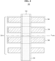
FIG. 3 is a cross-sectional view illustrating a three-dimensional flash memory according to an embodiment. -
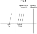
FIG. 4 is a diagram for a memory characteristic of a three-dimensional flash memory according to an embodiment. -
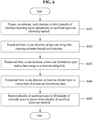
FIG. 5 is a flowchart illustrating a three-dimensional flash memory manufacturing method according to an embodiment. -
FIG. 6 is a flowchart illustrating a three-dimensional flash memory manufacturing method according to another embodiment. -
FIG. 7 is a cross-sectional view illustrating a three-dimensional flash memory according to an embodiment. -
FIGS. 8 and9 are diagrams for describing a multi-level of a three-dimensional flash memory according to an embodiment. -
FIGS. 10 and11 are cross-sectional views for describing a program operation of a three-dimensional flash memory according to an embodiment. -
FIG. 12 is a cross-sectional view for describing an erase operation of a three-dimensional flash memory according to an embodiment. -
FIG. 13 is a cross-sectional view for describing a read operation of a three-dimensional flash memory according to an embodiment. -
FIG. 14 is a flowchart illustrating a method of implementing a multi-level of a three-dimensional flash memory according to an embodiment. - Hereinafter, embodiments will be described in detail with reference to the accompanying drawings. However, the inventive concept are not limited or restricted by the embodiments.
- Further, the same reference signs/numerals in the drawings denote the same members. Furthermore, the terminologies used herein are used to properly express the embodiments of the inventive concept, and may be changed according to the intentions of the user or the manager or the custom in the field to which the inventive concept pertains. Accordingly, definition of the terms should be made according to the overall disclosure set forth herein.
-
FIG. 3 is a cross-sectional view illustrating a three-dimensional flash memory according to an embodiment, andFIG. 4 is a diagram for a memory characteristic of a three-dimensional flash memory according to an embodiment. - Referring to
FIGS. 3 and4 , a three-dimensional flash memory 300 according to an embodiment includes at least onechannel layer 310, at least oneferroelectric layer 320, and a plurality of electrode layers 330. - The at least one
channel layer 310 may be extended and formed in one direction (e.g., the z-axis direction inFIG. 2 ) on a substrate (not illustrated). In this case, the at least onechannel layer 310 may be formed by a selective epitaxial growth process or a phase change epitaxial process in which a substrate is used as a seed, and may further include a buried layer (not illustrated) that is disposed in a hollow tubular shape so as to fill the inside thereof as illustrated inFIG. 2 . - The at least one
channel layer 310 may be formed of a semiconductor material including Zn, In, Ga, a Group 4 semiconductor material, or a Group 3-5 compound having a C-axis aligned crystal (CAAC) crystal structure. As such, a cell current may increase, a leakage current may decrease, and a temperature-resistant reliability characteristic may be improved. For example, the at least onechannel layer 310 may be formed of a ZnOx-based material including at least one of AZO, ZTO, IZO, ITO, IGZO, and Ag-ZnO. However, the at least onechannel layer 310 is not limited thereto, and may be formed of single crystal silicon or poly-silicon like a conventional channel layer. - Also, although not illustrated in drawing, a drain line (not illustrated) may be connected on the at least one
channel layer 310. - The at least one
ferroelectric layer 320 is extended and formed in one direction to surround the at least onechannel layer 310 and is used as data storage. For example, the at least oneferroelectric layer 320 may be formed of a ferroelectric material of HfO2 having an orthorhombic crystal structure, and more specifically, may be formed of a ferroelectric material of HfO2 doped with at least one material of Al, Zr, or Si. For another example, the at least oneferroelectric layer 320 may be formed of a ferroelectric material including at least one of PZT(Pb(Zr, Ti)O3), PTO(PbTiO3), SBT(SrBi2Ti2O3), BLT(Bi(La, Ti)O3), PLZT(Pb(La, Zr)TiO3), BST(Bi(Sr, Ti)O3), barium titanate (BaTiO3), P(VDF-TrFE), PVDF, AIOx, ZnOx, TiOx, TaOx or InOx. - Below, that it is used as data storage means indicating (or storing) a value of binary data by using a voltage change according to a polarization phenomenon of a ferroelectric material forming the at least one
ferroelectric layer 320. - In this case, because the at least one
ferroelectric layer 320 is implemented with a single thin layer of 20 nm or less by using a ferroelectric material, a thickness of the at least oneferroelectric layer 320 may be markedly thin compared to the existing ONO layer. Accordingly, a low operation voltage may be used compared to a three-dimensional flash memory using the existing ONO layer, and the degree of integration in the horizontal direction may be improved. However, it is not limited or restricted thereto. For example, the at least oneferroelectric layer 320 may be formed of a plurality of thin layers, as well as a single thin layer. In this case, a total thickness of the plurality of thin layers may be maintained at 20 nm or less. - In particular, the at least one
ferroelectric layer 320 may be formed to have an operation voltage appropriate for a stable turn-on of the at least onechannel layer 310. In more detail, the at least oneferroelectric layer 320 is formed to satisfy a condition (i.e., a condition ofEquation 1 below) where a turn-on voltage of the at least onechannel layer 310 is smaller than an operation voltage of each ofmemory cells memory cells FIG. 4 , it should be satisfied a condition where a turn-onvoltage 410 of the at least onechannel layer 310 is smaller than anoperation voltage 420 of each of thememory cells threshold voltage 430 when each of thememory cells channel layer 310 that is 6 V (±6V) is smaller than 8V (±8V) being an operation voltage of each of thememory cells memory cells memory cells ferroelectric layer 320 and the plurality ofelectrode layers 330 are in contact with each other.
- In
Equation 1 above, "Cell Operation Voltage" means an operation voltage of each of thememory cells channel layer 310, and "Vth" means a threshold voltage when each of thememory cells - The above condition may be satisfied as a thickness of the at least one
ferroelectric layer 320 is adjusted. That is, a thickness of the at least oneferroelectric layer 320 may be adjusted to satisfy the condition where the turn-on voltage of the at least onechannel layer 310 is smaller than the operation voltage of each of thememory cells memory cells - Also, the above condition may be satisfied depending on a ferroelectric material forming the at least one
ferroelectric layer 320, as well as the thickness of the at least oneferroelectric layer 320. For example, to satisfy the condition where the turn-on voltage of the at least onechannel layer 310 is smaller than the operation voltage of each of thememory cells memory cells ferroelectric layer 320 may be formed of a ferroelectric material of HfO2 doped with at least one of Zr and Si to have a high polarization voltage. - The above characteristics may allow the three-
dimensional flash memory 300 according to an embodiment to be applied to string operations (e.g., a program operation, an erase operation, and a read operation) of an existing three-dimensional flash memory without modification. - Also, the at least one
ferroelectric layer 320 may have a multi-level based on the degree of a polarization phenomenon, that is, may have a multi-bit characteristic indicating data of a plurality of bits. The at least oneferroelectric layer 320 may be formed by using an atomic layer deposition (ALD) process to enable step coverage and nano-level thickness control. - The plurality of
electrode layers 330 are stacked to be vertically connected to the at least oneferroelectric layer 320 and are extended and formed in another direction (e.g., the y-axis direction inFIG. 2 ) perpendicular to the one direction. A conductive material such as tungsten, titanium, or tantalum may be used as a material for forming the plurality of electrode layers 330. - In the case of programming state "0" in which a threshold voltage is high, the three-
dimensional flash memory 300 with the above structure may apply an operation voltage for generating polarization to a gate electrode, with a voltage of the at least onechannel layer 310 maintained at 0 V or an appropriate reference voltage. In contrast, in the case of storing state "1" in which a threshold voltage is low (i.e., in the case of programming an erase state), the three-dimensional flash memory 300 may apply an operation voltage for inverting an existing polarization state to the at least onechannel layer 310, with a gate voltage maintained at 0 V or an appropriate reference voltage. - As the three-
dimensional flash memory 300 according to an embodiment uses the at least oneferroelectric layer 320 formed of a single thin layer as data storage, the degree of integration in the horizontal direction may be improved, and a reliability characteristic may be improved through a low operation voltage together with the improvement of the degree of integration. Also, as the at least onechannel layer 310 of the three-dimensional flash memory 300 is formed of a semiconductor material including Zn, In, Ga, a Group 4 semiconductor material, or a Group 3-5 compound having a C-axis aligned crystal (CAAC) crystal structure, a cell current may increase, a leakage current may decrease, and a temperature-resistant reliability characteristic may be improved. A method of manufacturing the three-dimensional flash memory 300 will be described in detail with reference toFIGS. 5 and6 . -
FIG. 5 is a flowchart illustrating a three-dimensional flash memory manufacturing method according to an embodiment. - Below, a three-dimensional flash memory manufactured by the three-dimensional flash memory manufacturing method includes the structure described above. Also, below, an automated and mechanized manufacturing system may be used as the subject performing the three-dimensional flash memory manufacturing method.
- Referring to
FIG. 5 , in step S510, the manufacturing system prepares, on a substrate, a mold structure in which a plurality of interlayer insulating layers and a plurality of electrode layers are stacked alternately. - Next, in step S520, the manufacturing system extends and forms at least one string hole, which penetrates the mold structure to expose the substrate, in one direction.
- Then, in step S530, the manufacturing system extends and forms at least one ferroelectric layer (the at least one ferroelectric layer including a vertical hole therein), which is used as data storage, in the at least one string hole. For example, the manufacturing system may form at least one ferroelectric layer using a ferroelectric material of HfO2 having an orthorhombic crystal structure. In more detail, the manufacturing system may form at least one ferroelectric layer using a ferroelectric material of HfO2 doped with at least one of Al, Zr, and Si.
- In particular, in step S530, the manufacturing system may implement a plurality of memory cells in regions being in contact with the plurality of electrode layers on the at least one ferroelectric layer, and may form the at least one ferroelectric layer such that there is satisfied the condition where a turn-on voltage of at least one channel layer is smaller than an operation voltage of each memory cell and is greater than a threshold voltage when each memory cell is programmed.
- In more detail, to satisfy the above condition, the manufacturing system may adjust a thickness of the at least one ferroelectric layer or may selectively determine a ferroelectric material for forming the at least one ferroelectric layer. For example, to satisfy the above condition, the manufacturing system may form at least one ferroelectric layer with a ferroelectric material of HfO2 doped with at least one of Zr and Si to have a high polarization voltage.
- Afterwards, in step S540, the manufacturing system extends and forms the at least one channel layer in the vertical hole of the at least one ferroelectric layer in one direction. In this case, the manufacturing system may form the at least one channel layer with a semiconductor material including Zn, In, Ga, a Group 4 semiconductor material or a Group 3-5 compound having a C-axis aligned crystal (CAAC) crystal structure.
- In the three-dimensional flash memory manufacturing method according to an embodiment, the manufacturing system may continuously perform step S530 and step S540 by using the ALD (Atomic Layer Deposition) process.
- The three-dimensional flash memory manufacturing method described above is not limited or restricted to step S510 to step S540, and may include various steps for manufacturing the three-dimensional flash memory described with reference to
FIG. 3 . For example, the three-dimensional flash memory described with reference toFIG. 3 may be manufactured by using a mold structure including a plurality of sacrificial layers, not a mold structure including a plurality of electrode layers. This will be described in detail with reference toFIG. 6 . -
FIG. 6 is a flowchart illustrating a three-dimensional flash memory manufacturing method according to another embodiment. - Below, a three-dimensional flash memory manufactured by the three-dimensional flash memory manufacturing method includes the structure described above. Also, below, an automated and mechanized manufacturing system may be used as the subject performing the three-dimensional flash memory manufacturing method.
- Referring to
FIG. 6 , in step S610, the manufacturing system prepares, on a substrate, a mold structure in which a plurality of interlayer insulating layers and a plurality of sacrificial layers are stacked alternately. - Next, in step S620, the manufacturing system extends and forms at least one string hole, which penetrates the mold structure to expose the substrate, in one direction.
- Then, in step S630, the manufacturing system extends and forms at least one ferroelectric layer (the at least one ferroelectric layer including a vertical hole therein), which is used as data storage, in the at least one string hole. For example, the manufacturing system may form at least one ferroelectric layer using a ferroelectric material of HfO2 having an orthorhombic crystal structure. In more detail, the manufacturing system may form at least one ferroelectric layer using a ferroelectric material of HfO2 doped with at least one of Al, Zr, and Si.
- In particular, in step S630, the manufacturing system may implement a plurality of memory cells in regions being in contact with the plurality of electrode layers on the at least one ferroelectric layer, and may form the at least one ferroelectric layer such that there is satisfied the condition where a turn-on voltage of at least one channel layer is smaller than an operation voltage of each memory cell and is greater than a threshold voltage when each memory cell is programmed.
- In more detail, to satisfy the above condition, the manufacturing system may adjust a thickness of the at least one ferroelectric layer or may selectively determine a ferroelectric material for forming the at least one ferroelectric layer. For example, to satisfy the above condition, the manufacturing system may form at least one ferroelectric layer with a ferroelectric material of HfO2 doped with at least one of Zr and Si to have a high polarization voltage.
- Afterwards, in step S640, the manufacturing system extends and forms the at least one channel layer in the vertical hole of the at least one ferroelectric layer in one direction. In this case, the manufacturing system may form the at least one channel layer with a semiconductor material including Zn, In, Ga, a Group 4 semiconductor material or a Group 3-5 compound having a C-axis aligned crystal (CAAC) crystal structure.
- In this case, in the three-dimensional flash memory manufacturing method according to another embodiment, the manufacturing system may continuously perform step S630 and step S640 by using the ALD process.
- Afterwards, in operation S650, the manufacturing system may remove the plurality of sacrificial layers and may fill the plurality of electrode layers in spaces where the plurality of sacrificial layers are removed.
- The three-dimensional flash memory manufacturing method described above is not limited or restricted to step S610 to step S650, and may include various steps for manufacturing the three-dimensional flash memory described with reference to
FIG. 3 . -
FIG. 7 is a cross-sectional view illustrating a three-dimensional flash memory according to an embodiment, andFIGS. 8 and9 are diagrams for describing a multi-level of a three-dimensional flash memory according to an embodiment. In detail,FIG. 8 is a diagram for describing how a polarization charge amount of at least one ferroelectric layer changes, in a three-dimensional flash memory according to an embodiment, andFIG. 9 is a diagram for describing each operation voltage when a three-dimensional flash memory according to an embodiment implements a multi-level. - Referring to
FIGS. 7 to 9 , a three-dimensional flash memory 700 according to an embodiment includes at least onechannel layer 710, a plurality ofelectrode layers 720, and at least oneferroelectric layer 730. - The at least one
channel layer 710 may be extended and formed in one direction (e.g., the z-axis direction inFIG. 2 ) on a substrate (not illustrated). In this case, the at least onechannel layer 710 may be formed by a selective epitaxial growth process or a phase change epitaxial process in which a substrate is used as a seed, and may further include a buried layer (not illustrated) that is disposed in a hollow tubular shape so as to fill the inside thereof as illustrated inFIG. 2 . - The at least one
channel layer 710 may be formed of a semiconductor material including Zn, In, Ga, a Group 4 semiconductor material, or a Group 3-5 compound having a C-axis aligned crystal (CAAC) crystal structure. As such, a cell current may increase, a leakage current may decrease, and a temperature-resistant reliability characteristic may be improved. For example, the at least onechannel layer 710 may be formed of a ZnOx-based material including at least one of AZO, ZTO, IZO, ITO, IGZO, and Ag-ZnO. However, the at least onechannel layer 710 is not limited thereto, and may be formed of single crystal silicon or poly-silicon like a conventional channel layer. - Also, although not illustrated in drawing, a drain line (not illustrated) may be connected on the at least one
channel layer 710. - The plurality of
electrode layers 720 are stacked to be perpendicular to the at least onechannel layer 710 and are extended and formed in another direction (e.g., the y-axis direction inFIG. 2 ) perpendicular to the one direction. A conductive material such as tungsten, titanium, or tantalum may be used as a material for forming the plurality of electrode layers 720. - The at least one
ferroelectric layer 730 surrounds the at least onechannel layer 710 and is interposed between the at least onechannel layer 710 and the plurality ofelectrode layers 720 in one direction (e.g., the z-axis direction inFIG. 2 ), and the at least oneferroelectric layer 730 is used as data storage as a plurality ofmemory cells ferroelectric layer 730 and the plurality ofelectrode layers 720 are in contact with each other. - In this case, the at least one
ferroelectric layer 730 may be formed of a ferroelectric material of HfO2 having an orthorhombic crystal structure, and for example, may be formed of a ferroelectric material of HfO2 doped with at least one material of Al, Zr, or Si. For another example, the at least oneferroelectric layer 730 may be formed of a ferroelectric material including at least one of PZT(Pb(Zr, Ti)O3), PTO(PbTiO3), SBT(SrBi2Ti2O3), BLT(Bi(La, Ti)O3), PLZT(Pb(La, Zr)TiO3), BST(Bi(Sr, Ti)O3), barium titanate (BaTiO3), P(VDF-TrFE), PVDF, AIOx, ZnOx, TiOx, TaOx or InOx. - Below, that it is used as data storage means that each of the regions of the at least one
ferroelectric layer 730 constituting the plurality ofmemory cells - Here, because the at least one
ferroelectric layer 730 is implemented with a single thin layer of 20 nm or less by using a ferroelectric material, a thickness of the at least oneferroelectric layer 720 may be markedly thin compared to the existing ONO layer. Accordingly, a low operation voltage may be used compared to a three-dimensional flash memory using the existing ONO layer, and the degree of integration in the horizontal direction may be improved. However, it is not limited or restricted thereto. For example, the at least oneferroelectric layer 730 may be formed of a plurality of thin layers, as well as a single thin layer. In this case, a total thickness of the plurality of thin layers may be maintained at 20 nm or less. - The three-
dimensional flash memory 700 with the above structure may implement a multi-level of atarget memory cell 733 by changing a polarization charge amount of a partial region of the at least oneferroelectric layer 730, which corresponds to thetarget memory cell 733 targeted for a program operation from among the plurality ofmemory cells ferroelectric layer 730 corresponding to thetarget memory cell 733 means thetarget memory cell 733 itself. - In more detail, a polarization charge amount corresponding when atoms of the
target memory cell 733 are polarized as shown in case (a) ofFIG. 8 is different from a polarization charge amount corresponding when atoms of thetarget memory cell 733 are polarized as shown in case (b). Likewise, polarization charge amounts respectively corresponding to case (c) and case (d) are different from the polarization charge amounts respectively corresponding to case (a) and case (b). - As such, the three-
dimensional flash memory 700 may change a polarization charge amount of thetarget memory cell 733 depending on the number of controlled atoms or a polarization rotation angle, by controlling the number of polarized atoms or a polarization rotation angle in thetarget memory cell 733. For example, like case (a), case (b), case (c), and case (d), the three-dimensional flash memory 700 may differently change a polarization charge amount of thetarget memory cell 733 by differently controlling the number of polarized atoms or a polarization rotation angle in thetarget memory cell 733. - In more detail, the three-
dimensional flash memory 700 may change a polarization charge amount of thetarget memory cell 733 so as to correspond to a first program state by controlling the number of polarized atoms or a polarization rotation angle in thetarget memory cell 733 like case (a), may change a polarization charge amount of thetarget memory cell 733 so as to correspond to a second program state by controlling the number of polarized atoms or a polarization rotation angle in thetarget memory cell 733 like case (c), may change a polarization charge amount of thetarget memory cell 733 so as to correspond to a third program state by controlling the number of polarized atoms or a polarization rotation angle in thetarget memory cell 733 like case (d), and may change a polarization charge amount of thetarget memory cell 733 so as to correspond to an erase state by controlling the number of polarized atoms or a polarization rotation angle in thetarget memory cell 733 like case (b). - In this case, the number of polarized atoms or a polarization rotation angle in the
target memory cell 733 may be controlled as a voltage to be applied to thetarget memory cell 733 is adjusted. That is, the three-dimensional flash memory 700 may change a polarization charge amount in thetarget memory cell 733, by adjusting a voltage to be applied to thetarget memory cell 733 between a negative value and a positive value such that the number of polarized atoms or a polarization rotation angle in thetarget memory cell 733 is controlled. - In this regard, referring to
FIG. 9 further, the three-dimensional flash memory 700 may apply a first program voltage of a negative value (e.g., -10 V) to thetarget memory cell 733 such that the number of polarized atoms or a polarization rotation angle in thetarget memory cell 733 is controlled as illustrated in case (a) ofFIG. 8 , that is, may program binary data of "00" by changing a polarization charge amount of thetarget memory cell 733 so as to correspond to the first program state. Likewise, the three-dimensional flash memory 700 may apply a second program voltage of a negative value (e.g., - 9 V) to thetarget memory cell 733 such that the number of polarized atoms or a polarization rotation angle in thetarget memory cell 733 is controlled as illustrated in case (c) ofFIG. 8 , that is, may program binary data of "01" by changing a polarization charge amount of thetarget memory cell 733 so as to correspond to the second program state, and may apply a third program voltage of a negative value (e.g., -8 V) to thetarget memory cell 733 such that the number of polarized atoms or a polarization rotation angle in thetarget memory cell 733 is controlled as illustrated in case (d) ofFIG. 8 , that is, may program binary data of "10" by changing a polarization charge amount of thetarget memory cell 733 so as to correspond to the third program state. - Also, the three-
dimensional flash memory 700 may apply a fourth program voltage of a positive value (e.g., 10V) to thetarget memory cell 733 such that the number of polarized atoms or a polarization rotation angle in thetarget memory cell 733 is controlled as illustrated in case (b) ofFIG. 8 , that is, may program binary data of "11" by changing a polarization charge amount of thetarget memory cell 733 so as to correspond to the fourth program state. The polarization charge amount of the fourth program state may be the polarization charge amount of the erase state described above, and the three-dimensional flash memory 700 may use the erase state of thetarget memory cell 733, which is caused by applying a voltage of a positive value to thetarget memory cell 733, as the fourth program state, thereby contributing a multi-level of thetarget memory cell 733. - That is, the three-
dimensional flash memory 700 may change a polarization charge amount of the at least oneferroelectric layer 730 between case (a) to case (d) ofFIG. 8 , by adjusting a program voltage to be applied to thetarget memory cell 733 between -10 V being a negative value and 10 V being a positive value like the above example. Accordingly, the three-dimensional flash memory 700 may implement a multi-level in which case (a) indicates binary data of "00", case (c) indicates binary data of "01", case (d) indicates binary data of "10", and case (d) indicates binary data of "11". - Here, a range between a negative value and a positive value, in which a program voltage to be applied to the
target memory cell 733 is adjusted, may be determined based on a thickness of the at least oneferroelectric layer 730 and a breakdown voltage of the at least oneferroelectric layer 730. In other words, the range between a negative value and a positive value, in which a program voltage to be applied to thetarget memory cell 733 is adjusted, may be determined based on a margin of a breakdown voltage according to a thickness of the at least oneferroelectric layer 730. For example, in the case where a thickness of the at least oneferroelectric layer 730 is 20 nm, a margin of a breakdown voltage of the at least oneferroelectric layer 730 may be about 16 V. In this case, the range between a negative value and a positive value, in which a program voltage to be applied to thetarget memory cell 733 is adjusted, may be determined as a range from -14 V to 10 V. For another example, in the case where a thickness of the at least oneferroelectric layer 730 is 15 nm, a margin of a breakdown voltage of the at least oneferroelectric layer 730 may be about 12V. In this case, the range between a negative value and a positive value, in which a program voltage to be applied to thetarget memory cell 733 is adjusted, may be determined as a range from -12 V to 10 V. - As such, the three-
dimensional flash memory 700 may adjust a program voltage to be applied to thetarget memory cell 733 in the range between a negative value and a positive value determined based on the thickness of the at least oneferroelectric layer 730 and the breakdown voltage of the at least oneferroelectric layer 730. - As described above, the three-
dimensional flash memory 700 may adjust a program voltage to be applied to thetarget memory cell 733 between a negative value and a positive value (e.g., may apply program voltages of different a negative value and a positive value to the target memory cell 733) such that a polarization charge amount of the at least oneferroelectric layer 730 changes, thereby implementing a multi-level of thetarget memory cell 733. - In this case, that program voltages of negative values are applied to the target memory cell 733 (i.e., the first, second, and third program voltages described above are applied thereto) may be performed by applying voltages of different negative values (i.e., a voltage of a negative value corresponding to the first program voltage, a voltage of a negative value corresponding to the second program voltage, and a voltage of a negative value corresponding to the third program voltage) to the
electrode layer 721 corresponding to thetarget memory cell 733 from among the plurality ofelectrode layers 720 and applying a voltage of 0 V to thechannel layer 710 of a string where thetarget memory cell 733 is placed or to thechannel layer 710 from the substrate corresponding to the string. - However, it is not limited or restricted thereto. For example, that program voltages of negative values are applied to the target memory cell 733 (i.e., the first, second, and third program voltages described above are applied thereto) may be performed by applying a voltage of 0 V to the
electrode layer 721 corresponding to thetarget memory cell 733 from among the plurality ofelectrode layers 720 and applying voltages of different positive voltages (i.e., a voltage of a positive value corresponding to the first program voltage, a voltage of a positive value corresponding to the second program voltage, and a voltage of a positive value corresponding to the third program voltage) to thechannel layer 710 of a string where thetarget memory cell 733 is placed or to thechannel layer 710 from the substrate corresponding to the string. - A way to apply a program voltage of a negative value to the
target memory cell 733 will be described with reference toFIGS. 10 and11 below. - An example in which the three-
dimensional flash memory 700 implements a multi-level of 2 bits is described above, but is not limited nor restricted thereto. A multi-level of 3 or more bits may also be implemented based on the same principle (i.e., a principle of implementing a multi-level by adjusting a program voltage to be applied to thetarget memory cell 733 between a negative value and a positive value such that a polarization charge amount of thetarget memory cell 733 changes). -
FIGS. 10 and11 are cross-sectional views for describing a program operation of a three-dimensional flash memory according to an embodiment. - Referring to
FIG. 10 , a three-dimensional flash memory 1000 may apply a program voltage of a negative value to atarget memory cell 1020 by applying a voltage of a negative value to anelectrode layer 1011 corresponding to thetarget memory cell 1020 of a plurality ofelectrode layers 1010 and applying a voltage of 0 V to a channel layer of a string where thetarget memory cell 1020 is placed or to a channel layer from a substrate corresponding to the string. In this case, a pass voltage may be applied to each of the remaining electrode layers other than theelectrode layer 1011 corresponding to thetarget memory cell 1020 from among the plurality of electrode layers 1010. - For example, for the
target memory cell 1020 to have a polarization charge amount corresponding to case (a) ofFIG. 8 , the three-dimensional flash memory 1000 may apply -10 V being a first program voltage to thetarget memory cell 1020. To this end, the three-dimensional flash memory 1000 may apply -10 V to theelectrode layer 1011 corresponding to thetarget memory cell 1020 of the plurality ofelectrode layers 1010 and may apply a voltage of 0 V to the channel layer of the string where thetarget memory cell 1020 is placed or to the channel layer from the substrate corresponding to the string, and thus, -10 V may be applied to thetarget memory cell 1020. - Like case (a), in case (c) and case (d) of
FIG. 8 , because a program voltage of a negative value is applied, the same manner may be used except that only a value of a voltage to be applied to theelectrode layer 1011 is changed (e.g., in case (c), -9 V is applied to theelectrode layer 1011; in case (d), -8 V is applied to the electrode layer 1011). In case (b), because a program voltage of a positive value is applied, an erase operation to be described with reference toFIG. 12 below may be utilized. - However, the way to apply a program voltage of a negative value to the
target memory cell 1020 is capable of being implemented in any other way, as well as the described way. In this regard, referring toFIG. 11 , a three-dimensional flash memory 1100 may apply a program voltage of a negative value to atarget memory cell 1120 by applying a voltage of 0 V to anelectrode layer 1111 corresponding to thetarget memory cell 1120 of a plurality ofelectrode layers 1110 and applying a voltage of a positive value to the channel layer of the string where thetarget memory cell 1120 is placed or to the channel layer from the substrate corresponding to the string. - Here, the voltage of the positive value applied to the channel layer of the string or to the channel layer from the substrate corresponding to the string may correspond to a result of changing a sign of a program voltage of a negative value to be applied to the
target memory cell 1120, as a value corresponding to the program voltage of the negative value to be applied to thetarget memory cell 1120. - For example, for the
target memory cell 1120 to have a polarization charge amount corresponding to case (a) ofFIG. 8 , the three-dimensional flash memory 1100 may apply -10 V being a first program voltage to thetarget memory cell 1120. To this end, the three-dimensional flash memory 1100 may apply 0 V to theelectrode layer 1111 corresponding to thetarget memory cell 1120 of the plurality ofelectrode layers 1110 and may apply a voltage of 10 V to the channel layer of the string where thetarget memory cell 1120 is placed or to the channel layer from the substrate corresponding to the string, and thus, 10 V may be applied to thetarget memory cell 1120. - Like case (a), in case (c) and case (d) of
FIG. 8 , because a program voltage of a negative value is applied, the same manner may be used except that only a value of a voltage to be applied to theelectrode layer 1111 is changed (e.g., in case (c), 9 V is applied to the channel layer of the string or to the channel layer from the substrate corresponding to the string; in case (d), 8 V is applied to the channel layer of the string or to the channel layer from the substrate corresponding to the string). In case (b), because a program voltage of a positive value is applied, an erase operation to be described with reference toFIG. 12 below may be utilized. -
FIG. 12 is a cross-sectional view for describing an erase operation of a three-dimensional flash memory according to an embodiment. - Referring to
FIG. 12 , a three-dimensional flash memory 1200 according to an embodiment may perform an erase operation on a plurality of memory cells included in the three-dimensional flash memory 1200 by applying an erase voltage (e.g., 10 V) to each of a plurality ofelectrode layers 1210 and applying a voltage of 0 V to a channel layer of each string or a channel layer from the substrate corresponding to the string. - A polarization charge amount that is determined after the erase operation may be used as one state for a multi-level of a
target memory cell 1220. That is, in the three-dimensional flash memory 1200, because an erase state of thetarget memory cell 1220 indicates one (e.g., "11") of binary data, an erase voltage of 10 V being a positive value to be applied to thetarget memory cell 1220 in the erase operation (i.e., an erase voltage of 10 V being a positive value to be applied to each of the plurality of electrode layers 1210) may be referred to as a "program voltage" of a positive value for programming binary data of "11". - Accordingly, as described with reference to
FIGS. 7 to 12 , a three-dimensional flash memory may apply program voltages of different negative values to a target memory cell and may apply a program voltage of a positive value (i.e., an erase voltage of a positive value) for utilization of an erase state, and thus, a multi-level of the three-dimensional flash memory may be implemented. - A read operation of the three-dimensional flash memory implementing the multi-level will be described with reference to
FIG. 13 below. -
FIG. 13 is a cross-sectional view for describing a read operation of a three-dimensional flash memory according to an embodiment. - Referring to
FIG. 13 , a three-dimensional flash memory 1300 may perform a read operation on atarget memory cell 1320 by applying 0 V to anelectrode layer 1311 corresponding to thetarget memory cell 1320 of a plurality ofelectrode layers 1310, applying a pass voltage to the remainingelectrode layers 1311, and applying a read voltage (e.g., 1 V) to a channel layer of a string where thetarget memory cell 1320 is placed or to a channel layer from the substrate corresponding to the string. As such, binary data, which thetarget memory cell 1320 indicates, from among multi-leveled binary data may be read. -
FIG. 14 is a flowchart illustrating a method of implementing a multi-level of a three-dimensional flash memory according to an embodiment. Below, the subject that performs a multi-level implementing method of a three-dimensional flash may be the three-dimensional flash memory described with reference toFIGS. 7 to 13 . - Referring to
FIG. 14 , in step S1410, a three-dimensional flash memory determines a range of a program voltage to be applied to a target memory cell targeted for a program operation from among a plurality of memory cells, between a negative value and a positive value. - In more detail, in step S1410, the three-dimensional flash memory may determine the range of the program voltage to be applied to the target memory cell between a negative value and a positive value, based on a thickness of at least one ferroelectric layer and a breakdown voltage of the at least one ferroelectric layer.
- Next, in step S1420, the three-dimensional flash memory adjusts the program voltage to be applied to the target memory cell in a range between a negative value and a positive value according to a determination result.
- In this case, to adjust the program voltage to be applied to the target memory cell in the range between the negative value and the positive value in step S1420 may mean to apply program voltages of different negative values and a program voltage of a positive value to the target memory cell.
- A first way or a second way may be used as a way to apply each of program voltages of different negative values to a target memory cell. According to the first way, a voltage of a negative value may be applied to an electrode layer corresponding to the target memory cell from among a plurality of electrode layers, a voltage of 0 V may be applied to a channel layer of a string where the target memory cell is placed or to a channel layer from the substrate corresponding to the string, and a program voltage of a negative value may be applied to the target memory cell. According to the second way, a voltage of 0 V may be applied to the electrode layer corresponding to the target memory cell from among the plurality of electrode layers, a voltage of a positive value may be applied to the channel layer of the string where the target memory cell is placed or to the channel layer from the substrate corresponding to the string, and a program voltage of a negative value may be applied to the target memory cell.
- Afterwards, in step S1430, the three-dimensional flash memory may adjust the program voltage to be applied to the target memory cell such that a polarization charge amount of a partial region of at least one ferroelectric layer corresponding to the target memory cell changes, and thus, a multi-level of the target memory cell is implemented.
- Case (a) to case (d) of
FIG. 8 will be described as an example of step S1410 to step S1430. The three-dimensional flash memory may determine a range of a program voltage to be applied to a target memory cell as -10 V to 10 V in step S1410. Then, in step S1420, the three-dimensional flash memory may apply a first program voltage (e.g., -10 V) being a negative value such that the target memory cell has a polarization charge amount corresponding to case (a) ofFIG. 8 , may apply a second program voltage (e.g., -9 V) being a negative value such that the target memory cell has a polarization charge amount corresponding to case (c) ofFIG. 8 , may apply a third program voltage (e.g., -8 V) being a negative value such that the target memory cell has a polarization charge amount corresponding to case (d) ofFIG. 8 , or may apply a fourth program voltage (e.g., 10 V) being a positive value such that the target memory cell has a polarization charge amount corresponding to case (b) ofFIG. 8 . Accordingly, the three-dimensional flash memory may implement a multi-level for the target memory cell in step S1430. - While a few embodiments have been shown and described with reference to the accompanying drawings, it will be apparent to those skilled in the art that various modifications and variations can be made from the foregoing descriptions. For example, adequate effects may be achieved even if the foregoing processes and methods are carried out in different order than described above, and/or the aforementioned elements, such as systems, structures, devices, or circuits, are combined or coupled in different forms and modes than as described above or be substituted or switched with other components or equivalents.
- Therefore, other implements, other embodiments, and equivalents to claims are within the scope of the following claims.
Claims (15)
- A three-dimensional flash memory comprising:at least one channel layer extended and formed in one direction;at least one ferroelectric layer extended and formed in the one direction to surround the at least one channel layer and used as data storage; anda plurality of electrode layers stacked to be vertically connected to the at least one ferroelectric layer.
- The three-dimensional flash memory of claim 1, wherein the at least one ferroelectric layer is formed to implement a plurality of memory cells in regions thereof being in contact with the plurality of electrode layers and to satisfy a condition where a turn-on voltage of the at least one channel layer is smaller than an operation voltage of each of the memory cells and is greater than a threshold voltage when each of the memory cells is programmed.
- The three-dimensional flash memory of claim 2, wherein a thickness of the at least one ferroelectric layer is adjusted to satisfy the condition.
- The three-dimensional flash memory of claim 1, wherein the at least one ferroelectric layer is formed of a ferroelectric material of HfO2 with an orthorhombic crystal structure.
- The three-dimensional flash memory of claim 1, wherein the at least one ferroelectric layer is formed of a ferroelectric material including at least one of PZT(Pb(Zr, Ti)O3), PTO(PbTiO3), SBT(SrBi2Ti2O3), BLT(Bi(La, Ti)O3), PLZT(Pb(La, Zr)TiO3), BST(Bi(Sr, Ti)O3), barium titanate (BaTiO3), P(VDF-TrFE), PVDF, AIOx, ZnOx, TiOx, TaOx or InOx.
- The three-dimensional flash memory of claim 1, wherein the at least one channel layer is formed of a semiconductor material including Zn, In, Ga, a Group 4 semiconductor material or a Group 3-5 compound having a C-axis aligned crystal (CAAC) crystal structure.
- At least one ferroelectric layer which is used in a three-dimensional flash memory including at least one channel layer extended and formed in one direction and a plurality of electrode layers stacked vertically to the at least one channel layer,
wherein the at least one ferroelectric layer is extended and formed in the one direction to surround the at least one channel layer, is used as data storage, and is formed to implement a plurality of memory cells in regions thereof being in contact with the plurality of electrode layers and to satisfy a condition where a turn-on voltage of the at least one channel layer is smaller than an operation voltage of each of the memory cells and is greater than a threshold voltage when each of the memory cells is programmed. - A method of manufacturing a three-dimensional flash memory comprising:preparing, on a substrate, a mold structure in which a plurality of interlayer insulating layers and a plurality of electrode layers are stacked alternately;extending and forming at least one string hole, which penetrates the mold structure to expose the substrate, in one direction;extending and forming at least one ferroelectric layer used as data storage in the at least one string hole, wherein the at least one ferroelectric layer includes a vertical hole therein; andextending and forming at least one channel layer in the vertical hole of the at least one ferroelectric layer in the one direction.
- A method of manufacturing a three-dimensional flash memory comprising:preparing, on a substrate, a mold structure in which a plurality of interlayer insulating layers and a plurality of sacrificial layers are stacked alternately;extending and forming at least one string hole, which penetrates the mold structure to expose the substrate, in one direction;extending and forming at least one ferroelectric layer used as data storage in the at least one string hole, wherein the at least one ferroelectric layer includes a vertical hole therein;extending and forming at least one channel layer in the vertical hole of the at least one ferroelectric layer in the one direction; andremoving the plurality of sacrificial layers and filling a plurality of electrode layers in spaces in which the plurality of sacrificial layers are removed.
- A ferroelectric material-based three-dimensional flash memory which implements a multi-level, the three-dimensional flash memory comprising:at least one channel layer extended and formed in one direction on a substrate;a plurality of electrode layers stacked to be perpendicular to the at least one channel layer; andat least one ferroelectric layer interposed between the at least one channel layer and the plurality of electrode layers in the one direction to surround the at least one channel layer and used as data storage to implement a plurality of memory cells in regions thereof being in contact with the plurality of electrode layers,wherein a multi-level for a target memory cell targeted for a program operation of the plurality of memory cells is implemented by changing a polarization charge amount of a partial region of the at least one ferroelectric layer corresponding to the target memory cell.
- The three-dimensional flash memory of claim 10, wherein the three-dimensional flash memory adjusts a program voltage to be applied to the target memory cell between a negative value and a positive value to change the polarization charge amount of the at least one ferroelectric layer.
- The three-dimensional flash memory of claim 11, wherein the three-dimensional flash memory applies program voltages of different a negative value and a positive value to the target memory cell between a negative value and a positive value to change the polarization charge amount of the at least one ferroelectric layer.
- The three-dimensional flash memory of claim 11, wherein the three-dimensional flash memory adjusts a program voltage to be applied to the target memory cell between a negative value and a positive value such that the number of polarized atoms or a polarization rotation angle in the partial region of the at least one ferroelectric layer changes, and changes the polarization charge amount depending on the number of polarized atoms or the polarization rotation angle thus controlled.
- A multi-level implementing method of a three-dimensional flash memory which includes at least one channel layer extended and formed in one direction on a substrate, a plurality of electrode layers stacked in a direction perpendicular to the at least one channel layer, and at least one ferroelectric layer interposed between the at least one channel layer and the plurality of electrode layers in the one direction to surround the at least one channel layer and used as data storage to implement a plurality of memory cells in regions thereof being in contact with the plurality of electrode layers, the method comprising:determining a range of a program voltage to be applied to a target memory cell targeted for a program operation from among the plurality of memory cells, between a negative value and a positive value;adjusting the program voltage to be applied to the target memory cell in a range between a negative value and a positive value according to the determination result; andimplementing a multi-level of the target memory cell by changing a polarization charge amount of a partial region of the at least one ferroelectric layer corresponding to the target memory cell, as the program voltage to be applied to the target memory cell is adjusted.
- The method of claim 14, wherein the determining includes:
determining the range of the program voltage to be applied to the target memory cell between a negative value and a positive value, based on a thickness of the at least one ferroelectric layer and a breakdown voltage of the at least one ferroelectric layer.
Applications Claiming Priority (3)
| Application Number | Priority Date | Filing Date | Title |
|---|---|---|---|
| KR1020190036909A KR102201016B1 (en) | 2019-03-29 | 2019-03-29 | Three dimensional flash memory based on ferro dielectric material and manufacturing method thereof |
| KR1020190090736A KR102219753B1 (en) | 2019-07-26 | 2019-07-26 | Three dimensional flash memory based on ferro dielectric material for implementing multi-level and operation method thereof |
| PCT/KR2019/018499 WO2020204314A1 (en) | 2019-03-29 | 2019-12-26 | Ferroelectric material-based three-dimensional flash memory, and manufacture therefor |
Publications (2)
| Publication Number | Publication Date |
|---|---|
| EP3951873A1 true EP3951873A1 (en) | 2022-02-09 |
| EP3951873A4 EP3951873A4 (en) | 2023-07-05 |
Family
ID=72667308
Family Applications (1)
| Application Number | Title | Priority Date | Filing Date |
|---|---|---|---|
| EP19923541.7A Pending EP3951873A4 (en) | 2019-03-29 | 2019-12-26 | FERROELECTRIC MATERIAL BASED THREE DIMENSIONAL FLASH MEMORY AND MANUFACTURE THEREOF |
Country Status (4)
| Country | Link |
|---|---|
| US (1) | US11515333B2 (en) |
| EP (1) | EP3951873A4 (en) |
| CN (1) | CN113330566B (en) |
| WO (1) | WO2020204314A1 (en) |
Families Citing this family (3)
| Publication number | Priority date | Publication date | Assignee | Title |
|---|---|---|---|---|
| KR102506456B1 (en) * | 2020-12-04 | 2023-03-07 | 포항공과대학교 산학협력단 | Semiconductor memory device and manufacturing method thereof |
| EP4071815A1 (en) * | 2021-04-07 | 2022-10-12 | Imec VZW | Vertical ferroelectric transistor with deposited oxide semiconductor channel |
| CN117769258A (en) * | 2022-09-14 | 2024-03-26 | 华为技术有限公司 | Ferroelectric memory, three-dimensional integrated circuits, electronic equipment |
Family Cites Families (20)
| Publication number | Priority date | Publication date | Assignee | Title |
|---|---|---|---|---|
| JPS6027160A (en) | 1983-07-25 | 1985-02-12 | Nippon Telegr & Teleph Corp <Ntt> | Semiconductor device |
| JP3202188B2 (en) | 1998-03-30 | 2001-08-27 | 株式会社日立製作所 | Semiconductor device |
| KR20140023806A (en) | 2012-08-17 | 2014-02-27 | 삼성전자주식회사 | Architecture of magnetic resistance memory device |
| JP2014053571A (en) * | 2012-09-10 | 2014-03-20 | Toshiba Corp | Ferroelectric memory and method of manufacturing the same |
| KR101421879B1 (en) * | 2013-01-15 | 2014-07-28 | 한양대학교 산학협력단 | Semiconductor memory device and method of forming the same |
| KR101511421B1 (en) | 2013-04-03 | 2015-04-10 | 한양대학교 산학협력단 | 3-Dimensional Memory of using Multi-layered Phase Change Material |
| US9558804B2 (en) * | 2014-07-23 | 2017-01-31 | Namlab Ggmbh | Charge storage ferroelectric memory hybrid and erase scheme |
| KR101944229B1 (en) | 2015-11-20 | 2019-01-30 | 샌디스크 테크놀로지스 엘엘씨 | Three-dimensional NAND device including support pedestal structures for buried source lines and method of manufacturing the same |
| US10892330B2 (en) * | 2016-07-06 | 2021-01-12 | International Business Machines Corporation | FET based synapse network |
| JP6758124B2 (en) * | 2016-08-29 | 2020-09-23 | 富士通セミコンダクターメモリソリューション株式会社 | Manufacturing method of 3D stacked chain type memory device |
| KR101872122B1 (en) | 2016-11-25 | 2018-06-27 | 연세대학교 산학협력단 | 3 dimensional ferroelectric memory device and method of fabricating the same |
| KR20180111304A (en) * | 2017-03-31 | 2018-10-11 | 에스케이하이닉스 주식회사 | Ferroelectric Memory Device |
| US9941299B1 (en) * | 2017-05-24 | 2018-04-10 | Sandisk Technologies Llc | Three-dimensional ferroelectric memory device and method of making thereof |
| KR20180134122A (en) * | 2017-06-08 | 2018-12-18 | 에스케이하이닉스 주식회사 | semiconductor device having ferroelectric layer and method of fabricating the same |
| KR20190026418A (en) | 2017-09-05 | 2019-03-13 | 에스케이하이닉스 주식회사 | Semiconductor memory device |
| JP2019057621A (en) * | 2017-09-21 | 2019-04-11 | 東芝メモリ株式会社 | Storage device |
| WO2019125352A1 (en) * | 2017-12-18 | 2019-06-27 | Intel Corporation | Three-dimensional integrated circuit memory cell having a ferroelectric field effect transistor with a floating gate |
| KR102025007B1 (en) * | 2018-02-23 | 2019-09-24 | 서울대학교산학협력단 | Non-volatile ferroelectric memory device and method of driving the same |
| KR102702091B1 (en) * | 2018-12-21 | 2024-09-04 | 삼성전자주식회사 | Memory device |
| KR102648581B1 (en) | 2019-01-16 | 2024-03-18 | 에스케이하이닉스 주식회사 | Semiconductor memory device |
-
2019
- 2019-12-26 EP EP19923541.7A patent/EP3951873A4/en active Pending
- 2019-12-26 WO PCT/KR2019/018499 patent/WO2020204314A1/en not_active Ceased
- 2019-12-26 CN CN201980089104.5A patent/CN113330566B/en active Active
- 2019-12-26 US US17/422,801 patent/US11515333B2/en active Active
Also Published As
| Publication number | Publication date |
|---|---|
| US20220130863A1 (en) | 2022-04-28 |
| CN113330566B (en) | 2024-10-15 |
| EP3951873A4 (en) | 2023-07-05 |
| US11515333B2 (en) | 2022-11-29 |
| WO2020204314A1 (en) | 2020-10-08 |
| CN113330566A (en) | 2021-08-31 |
Similar Documents
| Publication | Publication Date | Title |
|---|---|---|
| US11688462B2 (en) | Three-dimensional flash memory with back gate | |
| US12520497B2 (en) | Three-dimensional flash memory using ferroelectric layer on basis of back gate structure | |
| JP6581012B2 (en) | Semiconductor memory device and manufacturing method thereof | |
| US20210184044A1 (en) | Programmable Charge-Storage Transistor, An Array Of Elevationally-Extending Strings Of Memory Cells, And A Method Of Forming An Array Of Elevationally-Extending Strings Of Memory Cells | |
| US20250087272A1 (en) | Method for operating ferroelectric-based three-dimensional flash memory including data storage pattern | |
| US11515333B2 (en) | Ferroelectric material-based three-dimensional flash memory, and manufacture thereof | |
| KR102633429B1 (en) | 3d flash memory with extended memory window | |
| US20240087648A1 (en) | Three-dimensional flash memory for improving contact resistance of igzo channel layer | |
| KR102798552B1 (en) | Semiconducotr device and fabricating method thereof | |
| US12475951B2 (en) | Method for operating three-dimensional flash memory | |
| KR102219753B1 (en) | Three dimensional flash memory based on ferro dielectric material for implementing multi-level and operation method thereof | |
| KR102201016B1 (en) | Three dimensional flash memory based on ferro dielectric material and manufacturing method thereof | |
| KR102506204B1 (en) | 3d flash memory, operating method of the same and manufacturing method of the same | |
| KR102210330B1 (en) | Three dimensional flash memory based on ferro dielectric material for using multi step program operation and operation method thereof | |
| KR102373845B1 (en) | Three dimensional flash memory for performing memory operation based on hole injection by gidl | |
| US10056153B2 (en) | Semiconductor device and operating method of same | |
| US12374411B2 (en) | Three-dimensional flash memory for improving integration and operation method thereof | |
| KR102711886B1 (en) | Operation method of 3d flash memory including ferroelectric-based data storage pattern and back gate | |
| KR102565862B1 (en) | Three dimensional flash memory based on ferroelectric and operation method thereof | |
| US12620444B2 (en) | Operation method for three-dimensional flash memory including ferroelectric-based data storage pattern and back gate | |
| KR102886317B1 (en) | 3d memory including dual junction with asymmetric structure | |
| KR102628179B1 (en) | 3d memory, operating method of the same and manufacturing method of the same | |
| US20230284448A1 (en) | Three dimensional flash memory for improving leakage current | |
| US20240005991A1 (en) | Semiconductor storage device | |
| KR20100003965A (en) | Non-volatile memory device and method for fabricating the same |
Legal Events
| Date | Code | Title | Description |
|---|---|---|---|
| STAA | Information on the status of an ep patent application or granted ep patent |
Free format text: STATUS: THE INTERNATIONAL PUBLICATION HAS BEEN MADE |
|
| PUAI | Public reference made under article 153(3) epc to a published international application that has entered the european phase |
Free format text: ORIGINAL CODE: 0009012 |
|
| STAA | Information on the status of an ep patent application or granted ep patent |
Free format text: STATUS: REQUEST FOR EXAMINATION WAS MADE |
|
| 17P | Request for examination filed |
Effective date: 20211007 |
|
| AK | Designated contracting states |
Kind code of ref document: A1 Designated state(s): AL AT BE BG CH CY CZ DE DK EE ES FI FR GB GR HR HU IE IS IT LI LT LU LV MC MK MT NL NO PL PT RO RS SE SI SK SM TR |
|
| DAV | Request for validation of the european patent (deleted) | ||
| DAX | Request for extension of the european patent (deleted) | ||
| RIC1 | Information provided on ipc code assigned before grant |
Ipc: G11C 11/22 20060101ALI20221116BHEP Ipc: H01L 29/51 20060101ALI20221116BHEP Ipc: H01L 21/28 20060101ALI20221116BHEP Ipc: H01L 27/11524 20170101ALI20221116BHEP Ipc: H01L 27/11551 20170101ALI20221116BHEP Ipc: H01L 27/1159 20170101ALI20221116BHEP Ipc: H01L 27/11597 20170101AFI20221116BHEP |
|
| REG | Reference to a national code |
Ref country code: DE Ref legal event code: R079 Free format text: PREVIOUS MAIN CLASS: H01L0027115970 Ipc: H01L0021280000 |
|
| A4 | Supplementary search report drawn up and despatched |
Effective date: 20230605 |
|
| RIC1 | Information provided on ipc code assigned before grant |
Ipc: H10B 51/20 20230101ALI20230530BHEP Ipc: G11C 11/22 20060101ALI20230530BHEP Ipc: H01L 29/51 20060101ALI20230530BHEP Ipc: H01L 21/28 20060101AFI20230530BHEP |