EP3951815A1 - Power storage device - Google Patents
Power storage device Download PDFInfo
- Publication number
- EP3951815A1 EP3951815A1 EP20776850.8A EP20776850A EP3951815A1 EP 3951815 A1 EP3951815 A1 EP 3951815A1 EP 20776850 A EP20776850 A EP 20776850A EP 3951815 A1 EP3951815 A1 EP 3951815A1
- Authority
- EP
- European Patent Office
- Prior art keywords
- storage device
- power storage
- solid electrolyte
- electrolyte layer
- layer
- Prior art date
- Legal status (The legal status is an assumption and is not a legal conclusion. Google has not performed a legal analysis and makes no representation as to the accuracy of the status listed.)
- Withdrawn
Links
- 238000003860 storage Methods 0.000 title claims abstract description 141
- 239000010410 layer Substances 0.000 claims abstract description 174
- 239000007784 solid electrolyte Substances 0.000 claims abstract description 128
- 239000011247 coating layer Substances 0.000 claims abstract description 84
- 238000007747 plating Methods 0.000 claims description 53
- 239000011149 active material Substances 0.000 claims description 40
- 239000002223 garnet Substances 0.000 claims description 20
- 229910007822 Li2ZrO3 Inorganic materials 0.000 claims description 7
- 229910002984 Li7La3Zr2O12 Inorganic materials 0.000 claims description 7
- 229910002230 La2Zr2O7 Inorganic materials 0.000 claims description 5
- NINIDFKCEFEMDL-UHFFFAOYSA-N Sulfur Chemical compound [S] NINIDFKCEFEMDL-UHFFFAOYSA-N 0.000 claims description 4
- 229910052717 sulfur Inorganic materials 0.000 claims description 4
- 239000011593 sulfur Substances 0.000 claims description 4
- 238000000034 method Methods 0.000 description 25
- 239000000843 powder Substances 0.000 description 22
- 238000005245 sintering Methods 0.000 description 19
- 229910052751 metal Inorganic materials 0.000 description 18
- 239000002184 metal Substances 0.000 description 18
- 229920005989 resin Polymers 0.000 description 18
- 239000011347 resin Substances 0.000 description 18
- 229910000679 solder Inorganic materials 0.000 description 17
- 230000008569 process Effects 0.000 description 16
- 230000000694 effects Effects 0.000 description 14
- 239000000463 material Substances 0.000 description 14
- 239000000203 mixture Substances 0.000 description 12
- 238000010438 heat treatment Methods 0.000 description 11
- 239000013078 crystal Substances 0.000 description 10
- 239000011521 glass Substances 0.000 description 10
- 239000002344 surface layer Substances 0.000 description 10
- 230000007613 environmental effect Effects 0.000 description 7
- 239000007788 liquid Substances 0.000 description 7
- MCMNRKCIXSYSNV-UHFFFAOYSA-N Zirconium dioxide Chemical compound O=[Zr]=O MCMNRKCIXSYSNV-UHFFFAOYSA-N 0.000 description 6
- 230000015572 biosynthetic process Effects 0.000 description 6
- 239000003990 capacitor Substances 0.000 description 6
- 239000000470 constituent Substances 0.000 description 6
- 229910052802 copper Inorganic materials 0.000 description 6
- 238000010586 diagram Methods 0.000 description 6
- 229910052759 nickel Inorganic materials 0.000 description 6
- 239000000523 sample Substances 0.000 description 6
- 239000000654 additive Substances 0.000 description 5
- 238000005304 joining Methods 0.000 description 5
- 229910052746 lanthanum Inorganic materials 0.000 description 5
- 229910052763 palladium Inorganic materials 0.000 description 5
- KDLHZDBZIXYQEI-UHFFFAOYSA-N palladium Substances [Pd] KDLHZDBZIXYQEI-UHFFFAOYSA-N 0.000 description 5
- 239000002245 particle Substances 0.000 description 5
- 239000002994 raw material Substances 0.000 description 5
- 239000006104 solid solution Substances 0.000 description 5
- IJGRMHOSHXDMSA-UHFFFAOYSA-N Atomic nitrogen Chemical compound N#N IJGRMHOSHXDMSA-UHFFFAOYSA-N 0.000 description 4
- 229910052782 aluminium Inorganic materials 0.000 description 4
- 229910021645 metal ion Inorganic materials 0.000 description 4
- 239000007773 negative electrode material Substances 0.000 description 4
- 239000007774 positive electrode material Substances 0.000 description 4
- 229910052709 silver Inorganic materials 0.000 description 4
- 229910052779 Neodymium Inorganic materials 0.000 description 3
- 229910052777 Praseodymium Inorganic materials 0.000 description 3
- 238000002441 X-ray diffraction Methods 0.000 description 3
- 230000000996 additive effect Effects 0.000 description 3
- 229910045601 alloy Inorganic materials 0.000 description 3
- 239000000956 alloy Substances 0.000 description 3
- PNEYBMLMFCGWSK-UHFFFAOYSA-N aluminium oxide Inorganic materials [O-2].[O-2].[O-2].[Al+3].[Al+3] PNEYBMLMFCGWSK-UHFFFAOYSA-N 0.000 description 3
- 239000000969 carrier Substances 0.000 description 3
- 239000002482 conductive additive Substances 0.000 description 3
- 229910001416 lithium ion Inorganic materials 0.000 description 3
- 238000004519 manufacturing process Methods 0.000 description 3
- 150000002739 metals Chemical class 0.000 description 3
- 229910052758 niobium Inorganic materials 0.000 description 3
- 230000035515 penetration Effects 0.000 description 3
- 239000011148 porous material Substances 0.000 description 3
- 229910052761 rare earth metal Inorganic materials 0.000 description 3
- 150000002910 rare earth metals Chemical class 0.000 description 3
- 230000035939 shock Effects 0.000 description 3
- 230000007847 structural defect Effects 0.000 description 3
- 229910052718 tin Inorganic materials 0.000 description 3
- 230000008016 vaporization Effects 0.000 description 3
- HBBGRARXTFLTSG-UHFFFAOYSA-N Lithium ion Chemical compound [Li+] HBBGRARXTFLTSG-UHFFFAOYSA-N 0.000 description 2
- 239000004698 Polyethylene Substances 0.000 description 2
- XLOMVQKBTHCTTD-UHFFFAOYSA-N Zinc monoxide Chemical compound [Zn]=O XLOMVQKBTHCTTD-UHFFFAOYSA-N 0.000 description 2
- QVGXLLKOCUKJST-UHFFFAOYSA-N atomic oxygen Chemical compound [O] QVGXLLKOCUKJST-UHFFFAOYSA-N 0.000 description 2
- 239000011230 binding agent Substances 0.000 description 2
- 229910052797 bismuth Inorganic materials 0.000 description 2
- 239000003795 chemical substances by application Substances 0.000 description 2
- 238000005336 cracking Methods 0.000 description 2
- 238000009792 diffusion process Methods 0.000 description 2
- 239000000835 fiber Substances 0.000 description 2
- 229910052737 gold Inorganic materials 0.000 description 2
- 230000008018 melting Effects 0.000 description 2
- 238000002844 melting Methods 0.000 description 2
- 238000002156 mixing Methods 0.000 description 2
- 229910052757 nitrogen Inorganic materials 0.000 description 2
- 229910000510 noble metal Inorganic materials 0.000 description 2
- 229910052760 oxygen Inorganic materials 0.000 description 2
- 239000001301 oxygen Substances 0.000 description 2
- 230000000149 penetrating effect Effects 0.000 description 2
- 229910052697 platinum Inorganic materials 0.000 description 2
- 238000005498 polishing Methods 0.000 description 2
- -1 polyethylene Polymers 0.000 description 2
- 229920000573 polyethylene Polymers 0.000 description 2
- 230000002829 reductive effect Effects 0.000 description 2
- 230000000717 retained effect Effects 0.000 description 2
- 238000007789 sealing Methods 0.000 description 2
- 229910002076 stabilized zirconia Inorganic materials 0.000 description 2
- 229910052715 tantalum Inorganic materials 0.000 description 2
- XLYOFNOQVPJJNP-UHFFFAOYSA-N water Substances O XLYOFNOQVPJJNP-UHFFFAOYSA-N 0.000 description 2
- 229920002799 BoPET Polymers 0.000 description 1
- DKPFZGUDAPQIHT-UHFFFAOYSA-N Butyl acetate Natural products CCCCOC(C)=O DKPFZGUDAPQIHT-UHFFFAOYSA-N 0.000 description 1
- OKTJSMMVPCPJKN-UHFFFAOYSA-N Carbon Chemical compound [C] OKTJSMMVPCPJKN-UHFFFAOYSA-N 0.000 description 1
- 229920000049 Carbon (fiber) Polymers 0.000 description 1
- RWSOTUBLDIXVET-UHFFFAOYSA-N Dihydrogen sulfide Chemical compound S RWSOTUBLDIXVET-UHFFFAOYSA-N 0.000 description 1
- 229910000990 Ni alloy Inorganic materials 0.000 description 1
- 229910002637 Pr6O11 Inorganic materials 0.000 description 1
- 229910052772 Samarium Inorganic materials 0.000 description 1
- 239000006087 Silane Coupling Agent Substances 0.000 description 1
- 229910001128 Sn alloy Inorganic materials 0.000 description 1
- GWEVSGVZZGPLCZ-UHFFFAOYSA-N Titan oxide Chemical compound O=[Ti]=O GWEVSGVZZGPLCZ-UHFFFAOYSA-N 0.000 description 1
- 239000006230 acetylene black Substances 0.000 description 1
- 230000009471 action Effects 0.000 description 1
- XAGFODPZIPBFFR-UHFFFAOYSA-N aluminium Chemical compound [Al] XAGFODPZIPBFFR-UHFFFAOYSA-N 0.000 description 1
- 238000004458 analytical method Methods 0.000 description 1
- 229910021383 artificial graphite Inorganic materials 0.000 description 1
- 239000012298 atmosphere Substances 0.000 description 1
- 238000001354 calcination Methods 0.000 description 1
- 239000006229 carbon black Substances 0.000 description 1
- 235000019241 carbon black Nutrition 0.000 description 1
- 239000004917 carbon fiber Substances 0.000 description 1
- 230000015556 catabolic process Effects 0.000 description 1
- 239000000919 ceramic Substances 0.000 description 1
- 238000006243 chemical reaction Methods 0.000 description 1
- 239000011248 coating agent Substances 0.000 description 1
- 238000000576 coating method Methods 0.000 description 1
- 150000001875 compounds Chemical class 0.000 description 1
- 230000001010 compromised effect Effects 0.000 description 1
- 229920001940 conductive polymer Polymers 0.000 description 1
- 239000004020 conductor Substances 0.000 description 1
- RKTYLMNFRDHKIL-UHFFFAOYSA-N copper;5,10,15,20-tetraphenylporphyrin-22,24-diide Chemical compound [Cu+2].C1=CC(C(=C2C=CC([N-]2)=C(C=2C=CC=CC=2)C=2C=CC(N=2)=C(C=2C=CC=CC=2)C2=CC=C3[N-]2)C=2C=CC=CC=2)=NC1=C3C1=CC=CC=C1 RKTYLMNFRDHKIL-UHFFFAOYSA-N 0.000 description 1
- 238000006731 degradation reaction Methods 0.000 description 1
- 230000000593 degrading effect Effects 0.000 description 1
- 230000008021 deposition Effects 0.000 description 1
- NJLLQSBAHIKGKF-UHFFFAOYSA-N dipotassium dioxido(oxo)titanium Chemical compound [K+].[K+].[O-][Ti]([O-])=O NJLLQSBAHIKGKF-UHFFFAOYSA-N 0.000 description 1
- 238000007599 discharging Methods 0.000 description 1
- 238000007606 doctor blade method Methods 0.000 description 1
- 239000007772 electrode material Substances 0.000 description 1
- 239000002003 electrode paste Substances 0.000 description 1
- 238000011156 evaluation Methods 0.000 description 1
- 238000009499 grossing Methods 0.000 description 1
- FUZZWVXGSFPDMH-UHFFFAOYSA-N hexanoic acid Chemical compound CCCCCC(O)=O FUZZWVXGSFPDMH-UHFFFAOYSA-N 0.000 description 1
- 229910000037 hydrogen sulfide Inorganic materials 0.000 description 1
- 230000006872 improvement Effects 0.000 description 1
- 230000005764 inhibitory process Effects 0.000 description 1
- 150000002500 ions Chemical class 0.000 description 1
- 239000003273 ketjen black Substances 0.000 description 1
- XGZVUEUWXADBQD-UHFFFAOYSA-L lithium carbonate Chemical compound [Li+].[Li+].[O-]C([O-])=O XGZVUEUWXADBQD-UHFFFAOYSA-L 0.000 description 1
- 229910052808 lithium carbonate Inorganic materials 0.000 description 1
- 238000005259 measurement Methods 0.000 description 1
- 238000000691 measurement method Methods 0.000 description 1
- 229910044991 metal oxide Inorganic materials 0.000 description 1
- 150000004706 metal oxides Chemical class 0.000 description 1
- 229910021382 natural graphite Inorganic materials 0.000 description 1
- 230000003287 optical effect Effects 0.000 description 1
- SWELZOZIOHGSPA-UHFFFAOYSA-N palladium silver Chemical compound [Pd].[Ag] SWELZOZIOHGSPA-UHFFFAOYSA-N 0.000 description 1
- 230000036961 partial effect Effects 0.000 description 1
- 230000002093 peripheral effect Effects 0.000 description 1
- 230000035699 permeability Effects 0.000 description 1
- 229920002037 poly(vinyl butyral) polymer Polymers 0.000 description 1
- 229920000767 polyaniline Polymers 0.000 description 1
- 229920000128 polypyrrole Polymers 0.000 description 1
- 229920000123 polythiophene Polymers 0.000 description 1
- 239000002243 precursor Substances 0.000 description 1
- 238000007639 printing Methods 0.000 description 1
- 239000011241 protective layer Substances 0.000 description 1
- 230000009467 reduction Effects 0.000 description 1
- 230000002940 repellent Effects 0.000 description 1
- 239000005871 repellent Substances 0.000 description 1
- 238000007650 screen-printing Methods 0.000 description 1
- 239000004065 semiconductor Substances 0.000 description 1
- 239000002002 slurry Substances 0.000 description 1
- 239000000243 solution Substances 0.000 description 1
- 239000002904 solvent Substances 0.000 description 1
- 230000035882 stress Effects 0.000 description 1
- 239000000126 substance Substances 0.000 description 1
- 239000000758 substrate Substances 0.000 description 1
- TXEYQDLBPFQVAA-UHFFFAOYSA-N tetrafluoromethane Chemical compound FC(F)(F)F TXEYQDLBPFQVAA-UHFFFAOYSA-N 0.000 description 1
- 230000008646 thermal stress Effects 0.000 description 1
- OGIDPMRJRNCKJF-UHFFFAOYSA-N titanium oxide Inorganic materials [Ti]=O OGIDPMRJRNCKJF-UHFFFAOYSA-N 0.000 description 1
- 238000009834 vaporization Methods 0.000 description 1
- 229910052725 zinc Inorganic materials 0.000 description 1
- 239000011701 zinc Substances 0.000 description 1
- 239000011787 zinc oxide Substances 0.000 description 1
- 229910052726 zirconium Inorganic materials 0.000 description 1
Images


Classifications
-
- H—ELECTRICITY
- H01—ELECTRIC ELEMENTS
- H01M—PROCESSES OR MEANS, e.g. BATTERIES, FOR THE DIRECT CONVERSION OF CHEMICAL ENERGY INTO ELECTRICAL ENERGY
- H01M50/00—Constructional details or processes of manufacture of the non-active parts of electrochemical cells other than fuel cells, e.g. hybrid cells
- H01M50/40—Separators; Membranes; Diaphragms; Spacing elements inside cells
- H01M50/403—Manufacturing processes of separators, membranes or diaphragms
-
- H—ELECTRICITY
- H01—ELECTRIC ELEMENTS
- H01G—CAPACITORS; CAPACITORS, RECTIFIERS, DETECTORS, SWITCHING DEVICES, LIGHT-SENSITIVE OR TEMPERATURE-SENSITIVE DEVICES OF THE ELECTROLYTIC TYPE
- H01G11/00—Hybrid capacitors, i.e. capacitors having different positive and negative electrodes; Electric double-layer [EDL] capacitors; Processes for the manufacture thereof or of parts thereof
- H01G11/04—Hybrid capacitors
- H01G11/06—Hybrid capacitors with one of the electrodes allowing ions to be reversibly doped thereinto, e.g. lithium ion capacitors [LIC]
-
- H—ELECTRICITY
- H01—ELECTRIC ELEMENTS
- H01G—CAPACITORS; CAPACITORS, RECTIFIERS, DETECTORS, SWITCHING DEVICES, LIGHT-SENSITIVE OR TEMPERATURE-SENSITIVE DEVICES OF THE ELECTROLYTIC TYPE
- H01G11/00—Hybrid capacitors, i.e. capacitors having different positive and negative electrodes; Electric double-layer [EDL] capacitors; Processes for the manufacture thereof or of parts thereof
- H01G11/22—Electrodes
- H01G11/26—Electrodes characterised by their structure, e.g. multi-layered, porosity or surface features
-
- H—ELECTRICITY
- H01—ELECTRIC ELEMENTS
- H01G—CAPACITORS; CAPACITORS, RECTIFIERS, DETECTORS, SWITCHING DEVICES, LIGHT-SENSITIVE OR TEMPERATURE-SENSITIVE DEVICES OF THE ELECTROLYTIC TYPE
- H01G11/00—Hybrid capacitors, i.e. capacitors having different positive and negative electrodes; Electric double-layer [EDL] capacitors; Processes for the manufacture thereof or of parts thereof
- H01G11/22—Electrodes
- H01G11/30—Electrodes characterised by their material
- H01G11/50—Electrodes characterised by their material specially adapted for lithium-ion capacitors, e.g. for lithium-doping or for intercalation
-
- H—ELECTRICITY
- H01—ELECTRIC ELEMENTS
- H01G—CAPACITORS; CAPACITORS, RECTIFIERS, DETECTORS, SWITCHING DEVICES, LIGHT-SENSITIVE OR TEMPERATURE-SENSITIVE DEVICES OF THE ELECTROLYTIC TYPE
- H01G11/00—Hybrid capacitors, i.e. capacitors having different positive and negative electrodes; Electric double-layer [EDL] capacitors; Processes for the manufacture thereof or of parts thereof
- H01G11/54—Electrolytes
- H01G11/56—Solid electrolytes, e.g. gels; Additives therein
-
- H—ELECTRICITY
- H01—ELECTRIC ELEMENTS
- H01M—PROCESSES OR MEANS, e.g. BATTERIES, FOR THE DIRECT CONVERSION OF CHEMICAL ENERGY INTO ELECTRICAL ENERGY
- H01M10/00—Secondary cells; Manufacture thereof
- H01M10/05—Accumulators with non-aqueous electrolyte
- H01M10/052—Li-accumulators
-
- H—ELECTRICITY
- H01—ELECTRIC ELEMENTS
- H01M—PROCESSES OR MEANS, e.g. BATTERIES, FOR THE DIRECT CONVERSION OF CHEMICAL ENERGY INTO ELECTRICAL ENERGY
- H01M10/00—Secondary cells; Manufacture thereof
- H01M10/05—Accumulators with non-aqueous electrolyte
- H01M10/052—Li-accumulators
- H01M10/0525—Rocking-chair batteries, i.e. batteries with lithium insertion or intercalation in both electrodes; Lithium-ion batteries
-
- H—ELECTRICITY
- H01—ELECTRIC ELEMENTS
- H01M—PROCESSES OR MEANS, e.g. BATTERIES, FOR THE DIRECT CONVERSION OF CHEMICAL ENERGY INTO ELECTRICAL ENERGY
- H01M10/00—Secondary cells; Manufacture thereof
- H01M10/05—Accumulators with non-aqueous electrolyte
- H01M10/056—Accumulators with non-aqueous electrolyte characterised by the materials used as electrolytes, e.g. mixed inorganic/organic electrolytes
- H01M10/0561—Accumulators with non-aqueous electrolyte characterised by the materials used as electrolytes, e.g. mixed inorganic/organic electrolytes the electrolyte being constituted of inorganic materials only
- H01M10/0562—Solid materials
-
- H—ELECTRICITY
- H01—ELECTRIC ELEMENTS
- H01M—PROCESSES OR MEANS, e.g. BATTERIES, FOR THE DIRECT CONVERSION OF CHEMICAL ENERGY INTO ELECTRICAL ENERGY
- H01M10/00—Secondary cells; Manufacture thereof
- H01M10/05—Accumulators with non-aqueous electrolyte
- H01M10/058—Construction or manufacture
- H01M10/0585—Construction or manufacture of accumulators having only flat construction elements, i.e. flat positive electrodes, flat negative electrodes and flat separators
-
- H—ELECTRICITY
- H01—ELECTRIC ELEMENTS
- H01M—PROCESSES OR MEANS, e.g. BATTERIES, FOR THE DIRECT CONVERSION OF CHEMICAL ENERGY INTO ELECTRICAL ENERGY
- H01M4/00—Electrodes
- H01M4/02—Electrodes composed of, or comprising, active material
- H01M4/36—Selection of substances as active materials, active masses, active liquids
- H01M4/48—Selection of substances as active materials, active masses, active liquids of inorganic oxides or hydroxides
-
- H—ELECTRICITY
- H01—ELECTRIC ELEMENTS
- H01M—PROCESSES OR MEANS, e.g. BATTERIES, FOR THE DIRECT CONVERSION OF CHEMICAL ENERGY INTO ELECTRICAL ENERGY
- H01M50/00—Constructional details or processes of manufacture of the non-active parts of electrochemical cells other than fuel cells, e.g. hybrid cells
- H01M50/40—Separators; Membranes; Diaphragms; Spacing elements inside cells
- H01M50/409—Separators, membranes or diaphragms characterised by the material
- H01M50/411—Organic material
- H01M50/414—Synthetic resins, e.g. thermoplastics or thermosetting resins
- H01M50/417—Polyolefins
-
- H—ELECTRICITY
- H01—ELECTRIC ELEMENTS
- H01M—PROCESSES OR MEANS, e.g. BATTERIES, FOR THE DIRECT CONVERSION OF CHEMICAL ENERGY INTO ELECTRICAL ENERGY
- H01M50/00—Constructional details or processes of manufacture of the non-active parts of electrochemical cells other than fuel cells, e.g. hybrid cells
- H01M50/40—Separators; Membranes; Diaphragms; Spacing elements inside cells
- H01M50/409—Separators, membranes or diaphragms characterised by the material
- H01M50/431—Inorganic material
- H01M50/434—Ceramics
-
- H—ELECTRICITY
- H01—ELECTRIC ELEMENTS
- H01M—PROCESSES OR MEANS, e.g. BATTERIES, FOR THE DIRECT CONVERSION OF CHEMICAL ENERGY INTO ELECTRICAL ENERGY
- H01M50/00—Constructional details or processes of manufacture of the non-active parts of electrochemical cells other than fuel cells, e.g. hybrid cells
- H01M50/40—Separators; Membranes; Diaphragms; Spacing elements inside cells
- H01M50/409—Separators, membranes or diaphragms characterised by the material
- H01M50/449—Separators, membranes or diaphragms characterised by the material having a layered structure
- H01M50/451—Separators, membranes or diaphragms characterised by the material having a layered structure comprising layers of only organic material and layers containing inorganic material
-
- H—ELECTRICITY
- H01—ELECTRIC ELEMENTS
- H01M—PROCESSES OR MEANS, e.g. BATTERIES, FOR THE DIRECT CONVERSION OF CHEMICAL ENERGY INTO ELECTRICAL ENERGY
- H01M50/00—Constructional details or processes of manufacture of the non-active parts of electrochemical cells other than fuel cells, e.g. hybrid cells
- H01M50/40—Separators; Membranes; Diaphragms; Spacing elements inside cells
- H01M50/489—Separators, membranes, diaphragms or spacing elements inside the cells, characterised by their physical properties, e.g. swelling degree, hydrophilicity or shut down properties
- H01M50/497—Ionic conductivity
-
- H—ELECTRICITY
- H01—ELECTRIC ELEMENTS
- H01G—CAPACITORS; CAPACITORS, RECTIFIERS, DETECTORS, SWITCHING DEVICES, LIGHT-SENSITIVE OR TEMPERATURE-SENSITIVE DEVICES OF THE ELECTROLYTIC TYPE
- H01G11/00—Hybrid capacitors, i.e. capacitors having different positive and negative electrodes; Electric double-layer [EDL] capacitors; Processes for the manufacture thereof or of parts thereof
- H01G11/10—Multiple hybrid or EDL capacitors, e.g. arrays or modules
- H01G11/12—Stacked hybrid or EDL capacitors
-
- H—ELECTRICITY
- H01—ELECTRIC ELEMENTS
- H01G—CAPACITORS; CAPACITORS, RECTIFIERS, DETECTORS, SWITCHING DEVICES, LIGHT-SENSITIVE OR TEMPERATURE-SENSITIVE DEVICES OF THE ELECTROLYTIC TYPE
- H01G11/00—Hybrid capacitors, i.e. capacitors having different positive and negative electrodes; Electric double-layer [EDL] capacitors; Processes for the manufacture thereof or of parts thereof
- H01G11/66—Current collectors
-
- H—ELECTRICITY
- H01—ELECTRIC ELEMENTS
- H01G—CAPACITORS; CAPACITORS, RECTIFIERS, DETECTORS, SWITCHING DEVICES, LIGHT-SENSITIVE OR TEMPERATURE-SENSITIVE DEVICES OF THE ELECTROLYTIC TYPE
- H01G11/00—Hybrid capacitors, i.e. capacitors having different positive and negative electrodes; Electric double-layer [EDL] capacitors; Processes for the manufacture thereof or of parts thereof
- H01G11/74—Terminals, e.g. extensions of current collectors
- H01G11/76—Terminals, e.g. extensions of current collectors specially adapted for integration in multiple or stacked hybrid or EDL capacitors
-
- H—ELECTRICITY
- H01—ELECTRIC ELEMENTS
- H01M—PROCESSES OR MEANS, e.g. BATTERIES, FOR THE DIRECT CONVERSION OF CHEMICAL ENERGY INTO ELECTRICAL ENERGY
- H01M4/00—Electrodes
- H01M4/02—Electrodes composed of, or comprising, active material
- H01M2004/021—Physical characteristics, e.g. porosity, surface area
-
- H—ELECTRICITY
- H01—ELECTRIC ELEMENTS
- H01M—PROCESSES OR MEANS, e.g. BATTERIES, FOR THE DIRECT CONVERSION OF CHEMICAL ENERGY INTO ELECTRICAL ENERGY
- H01M2300/00—Electrolytes
- H01M2300/0017—Non-aqueous electrolytes
- H01M2300/0065—Solid electrolytes
- H01M2300/0068—Solid electrolytes inorganic
-
- H—ELECTRICITY
- H01—ELECTRIC ELEMENTS
- H01M—PROCESSES OR MEANS, e.g. BATTERIES, FOR THE DIRECT CONVERSION OF CHEMICAL ENERGY INTO ELECTRICAL ENERGY
- H01M2300/00—Electrolytes
- H01M2300/0088—Composites
- H01M2300/0094—Composites in the form of layered products, e.g. coatings
-
- H—ELECTRICITY
- H01—ELECTRIC ELEMENTS
- H01M—PROCESSES OR MEANS, e.g. BATTERIES, FOR THE DIRECT CONVERSION OF CHEMICAL ENERGY INTO ELECTRICAL ENERGY
- H01M50/00—Constructional details or processes of manufacture of the non-active parts of electrochemical cells other than fuel cells, e.g. hybrid cells
- H01M50/50—Current conducting connections for cells or batteries
- H01M50/543—Terminals
- H01M50/562—Terminals characterised by the material
-
- Y—GENERAL TAGGING OF NEW TECHNOLOGICAL DEVELOPMENTS; GENERAL TAGGING OF CROSS-SECTIONAL TECHNOLOGIES SPANNING OVER SEVERAL SECTIONS OF THE IPC; TECHNICAL SUBJECTS COVERED BY FORMER USPC CROSS-REFERENCE ART COLLECTIONS [XRACs] AND DIGESTS
- Y02—TECHNOLOGIES OR APPLICATIONS FOR MITIGATION OR ADAPTATION AGAINST CLIMATE CHANGE
- Y02E—REDUCTION OF GREENHOUSE GAS [GHG] EMISSIONS, RELATED TO ENERGY GENERATION, TRANSMISSION OR DISTRIBUTION
- Y02E60/00—Enabling technologies; Technologies with a potential or indirect contribution to GHG emissions mitigation
- Y02E60/10—Energy storage using batteries
-
- Y—GENERAL TAGGING OF NEW TECHNOLOGICAL DEVELOPMENTS; GENERAL TAGGING OF CROSS-SECTIONAL TECHNOLOGIES SPANNING OVER SEVERAL SECTIONS OF THE IPC; TECHNICAL SUBJECTS COVERED BY FORMER USPC CROSS-REFERENCE ART COLLECTIONS [XRACs] AND DIGESTS
- Y02—TECHNOLOGIES OR APPLICATIONS FOR MITIGATION OR ADAPTATION AGAINST CLIMATE CHANGE
- Y02P—CLIMATE CHANGE MITIGATION TECHNOLOGIES IN THE PRODUCTION OR PROCESSING OF GOODS
- Y02P70/00—Climate change mitigation technologies in the production process for final industrial or consumer products
- Y02P70/50—Manufacturing or production processes characterised by the final manufactured product
Definitions
- the present disclosure relates to a power storage device in which a solid electrolyte is used.
- Patent Literature 1 discloses a battery in which a solid electrolyte structure made of a garnet-type crystal Li 7 L 3 Zr 2 O 12 is included, and a surface of the structure is coated with a resin.
- Patent Literature 2 discloses a battery in which Li 7 La 3 Zr 2 O 12 is used as a solid electrolyte, and an insulating layer is used between a positive electrode or a negative electrode and the solid electrolyte.
- An object of the present disclosure is to provide a surface-mount power storage device.
- the present disclosure provides a power storage device.
- the power storage device includes
- the coating layer has a conductivity less than a conductivity of the solid electrolyte layer, and the coating layer has a thickness of greater than or equal to 1 ⁇ m and less than or equal to 100 ⁇ m.
- a power storage device includes:
- the coating layer has a conductivity less than a conductivity of the solid electrolyte layer, and the coating layer has a thickness of greater than or equal to 1 ⁇ m and less than or equal to 100 ⁇ m.
- the power storage device provided is suitable for solder mounting.
- the power storage device of the first aspect may be such that, for example, the power storage device further includes an active material layer disposed inside the solid electrolyte layer.
- the power storage device provided is suitable for solder mounting.
- the power storage device according to the first or second aspect may be such that, for example, the solid electrolyte layer is a sintered body. With this configuration, the power storage device provided is suitable for solder mounting.
- the power storage device according to any one of the first to third aspects may be such that, for example, the solid electrolyte layer has a garnet structure. With this configuration, the power storage device provided is suitable for solder mounting.
- the power storage device according to any one of the first to fourth aspects may be such that, for example, the solid electrolyte layer contains no sulfur. With this configuration, the power storage device provided is suitable for solder mounting.
- the power storage device may be such that, for example, the solid electrolyte layer includes a crystalline phase including at least one selected from the group consisting of Li 7 La 3 Zr 2 O 12 and Li 7 Pr 3 Zr 2 O 12 .
- the power storage device provided is suitable for solder mounting.
- the power storage device according to any one of the first to sixth aspects may be such that, for example, the coating layer has a conductivity of less than or equal to 10 -4 S/cm. With this configuration, the power storage device provided is suitable for solder mounting.
- the power storage device according to any one of the first to seventh aspects may be such that, for example, the coating layer includes an oxide.
- the power storage device provided is suitable for solder mounting.
- the power storage device according to the eighth aspect may be such that, for example, the oxide includes a pyrochlore oxide. With this configuration, the power storage device provided is suitable for solder mounting.
- the power storage device according to the ninth aspect may be such that, for example, the pyrochlore oxide includes at least one selected from the group consisting of La 2 Zr 2 O 7 and Pr 2 Zr 2 O 7 .
- the power storage device provided is suitable for solder mounting.
- the power storage device may be such that, for example, the coating layer includes a crystalline phase including Li 2 ZrO 3 .
- the power storage device provided is suitable for solder mounting.
- the power storage device according to any one of the first to eleventh aspects may be such that, for example, the coating layer has a Li content molar ratio less than a Li content molar ratio of the solid electrolyte layer.
- the power storage device provided is suitable for solder mounting.
- the power storage device according to any one of the first to twelfth aspects may be such that, for example, the coating layer has a thickness of greater than or equal to 5 ⁇ m and less than or equal to 100 ⁇ m. With this configuration, the power storage device provided is suitable for solder mounting.
- the power storage device may be such that, for example, the power storage device further includes a plating that coats a surface of the first external electrode and a surface of the second external electrode.
- the power storage device provided is suitable for solder mounting.
- the power storage device according to any one of the first to fourteenth aspects may be such that, for example, the plating has a thickness of greater than or equal to 1 ⁇ m and less than or equal to 10 ⁇ m. With this configuration, the power storage device provided is suitable for solder mounting.
- the power storage device may be an all-solid-state battery or a capacitor.
- Fig. 1 is a cross-sectional view of a power storage device 1000, according to a first embodiment.
- the power storage device 1000 is an all-solid-state battery.
- the power storage device 1000 may be referred to as a "battery 1000".
- a first external electrode and a second external electrode may be collectively referred to as "terminal electrodes”.
- a first internal electrode may be referred to as a "first current collector”
- a second internal electrode may be referred to as a "second current collector”.
- the power storage device 1000 includes a solid electrolyte layer 400, a coating layer 600, a first internal electrode 310, a first external electrode 510, a second internal electrode 320, and a second external electrode 520.
- the first internal electrode 310 is disposed inside the solid electrolyte layer 400.
- the first external electrode 510 is disposed outside of the solid electrolyte layer 400 and electrically connected to the first internal electrode 310.
- the second internal electrode 320 is disposed inside the solid electrolyte layer 400.
- the second external electrode 520 is disposed outside of the solid electrolyte layer 400 and electrically connected to the second internal electrode 320.
- the coating layer 600 coats a surface of the solid electrolyte layer 400.
- the coating layer 600 has a conductivity less than a conductivity of the solid electrolyte layer 400.
- the conductivity of the coating layer 600 may be one or more orders of magnitude less than the conductivity of the solid electrolyte layer 400 and, for example, may be less than or equal to 10 -4 S/cm.
- the coating layer 600 may be, for example, an insulating layer.
- the power storage device 1000 may include an active material layer disposed inside the solid electrolyte layer 400.
- the power storage device 1000 may include an active material layer, which may be a first active material layer 110.
- the first active material layer 110 may be disposed inside the solid electrolyte layer 400 and on the first internal electrode 310 and may be electrically connected to the first external electrode 510.
- the power storage device 1000 may include an active material layer, which may be a second active material layer 120.
- the second active material layer 120 may be disposed inside the solid electrolyte layer 400 and on the second internal electrode 320 and may be electrically connected to the second external electrode 520.
- the first active material layer 110 may be disposed to face the second active material layer 120 with the solid electrolyte layer 400 disposed therebetween.
- the solid electrolyte layer 400 is, for example, a sintered body.
- a material of the solid electrolyte layer 400 include materials having a crystal structure of a garnet structure, materials having a crystal structure that has a NASICON-type structure, and materials having a perovskite-type crystal structure.
- the solid electrolyte layer 400 is a material having a crystal structure of a garnet structure.
- the solid electrolyte layer 400 is a sulfur-free material.
- the solid electrolyte layer 400 may include a crystalline phase including Li 7 La 3 Zr 2 O 12 or Li 7 Pr 3 Zr 2 O 12 .
- the coating layer 600 may include an oxide, for example.
- the oxide may include a pyrochlore oxide, for example.
- the pyrochlore oxide may include La 2 Zr 2 O 7 or Pr 2 Zr 2 O 7 , for example.
- the coating layer 600 may include a crystalline phase including Li 2 ZrO 3 , for example.
- the coating layer 600 may have a Li content molar ratio less than a Li content molar ratio of the solid electrolyte layer 400.
- the coating layer 600 has a thickness of greater than or equal to 1 ⁇ m and less than or equal to 100 ⁇ m. If the thickness of the coating layer 600 is less than 1 ⁇ m, the coating layer dissolves into a plating liquid during the formation of the plating layer on the terminal electrode, and as a result, the insulating property of the surface of the solid electrolyte layer is not ensured. Furthermore, moisture can easily penetrate the surface of the solid electrolyte layer, that is, moisture resistance is degraded. If the thickness of the coating layer 600 is greater than 100 ⁇ m, cracking or peeling of the coating layer occurs due to a cooling-heating cycle or handling, and as a result, the insulating property of the surface of the solid electrolyte layer is not ensured.
- the thickness of the coating layer 600 may be greater than or equal to 5 ⁇ m and less than or equal to 100 ⁇ m, for example.
- a sintered device can be tumble-polished while the coating layer is retained thereon. Accordingly, smoothing of a surface of the sintered device and chamfering of the four corners and edges can be accomplished, and, consequently, improvement in flexural strength and inhibition of chipping in the sintered device are realized.
- the constituent elements of the coating layer 600 may be similar to those of the solid electrolyte layer 400.
- the solid electrolyte layer 400 and coating layer 600 may both be an oxide.
- the solid electrolyte layer 400 may include a crystalline phase including Li 7 La 3 Zr 2 O 12 or Li 7 Pr 3 Zr 2 O 12
- the coating layer 600 may include an oxide of the solid electrolyte layer 400.
- the oxide of the solid electrolyte layer 400 may include at least one of a pyrochlore oxide (e.g., La 2 Zr 2 O 7 or Pr 2 Zr 2 O 7 ) or Li 2 ZrO 3 .
- joining interfaces of the solid electrolyte layer 400 and the coating layer 600 have similar coefficients of thermal expansion and therefore have a high degree of matching; hence, high thermal shock resistance is achieved compared insidestances in which a solid electrolyte is coated with a resin or a glass. Consequently, in solder mounting, the occurrence of cracking at the interfaces is inhibited, and excellent thermal resistance is exhibited. Accordingly, suitability for surface mounting is achieved.
- the "thermal resistance” refers to durability against the heat treatment in the so-called solder reflow. Furthermore, in actual usage, excellent thermal stress, such as a cooling-heating cycle, is exhibited. As a result of these advantageous effects, suitability for surface mounting and high reliability are realized.
- the solid electrolyte layer 400 includes a crystalline phase including Li 7 La 3 Zr 2 O 12 or Li 7 Pr 3 Zr 2 O 12
- sintering or heat treatment of an unsintered, green device of the solid electrolyte layer 400 results in the formation of a coating layer 600 including a pyrochlore oxide. Consequently, the solid electrolyte layer 400 and the coating layer 600 are formed with a mutually diffused continuous joining interface without a gap. Accordingly, high joining strength is achieved because of the strong bond due to a sintered structure, compared with sintered devices having a resin coating on the surface. As a result of this advantageous effect, high environmental resistance is achieved without causing problems, such as a problem with a plating liquid or moisture penetrating the joining interface.
- a plating process can be performed on the terminal electrodes without causing the plating to be unnecessarily deposited on regions other than the terminal electrodes. Consequently, a power storage device, as illustrated in Fig. 2 , that is suitable for surface mounting and has excellent environmental resistance, such as resistance to impact and thermal shock, is realized.
- the coating layer 600 may include a crystalline phase including Li 2 ZrO 3 , which has a conductivity less than a conductivity of a crystalline phase having a garnet structure.
- the formed coating layer 600 has high adhesion to the solid electrolyte layer 400, that is, the obtained coating layer 600 has excellent environmental resistance, such as resistance to impact and thermal shock.
- the Li content molar ratio in the coating layer 600 may be less than the Li content molar ratio in the solid electrolyte layer 400.
- the coating layer 600 has reduced conductivity because of the reduction in carriers. As a result, the coating layer 600 has the same effects as the effects described above.
- a plating process can be performed on the terminal electrodes without causing the plating to be unnecessarily deposited on regions other than the terminal electrodes. Hence, a surface-mount power storage device is realized.
- the "sintered device” is defined, for example, as a device formed of a combination of the sintered body of the solid electrolyte layer 400, the first internal electrode 310 and the second internal electrode 320, which are included as current collectors inside the sintered body, and the coating layer 600.
- the sintered device is formed of a solid solution composition and the coating layer 600, which coats a surface thereof, and the solid solution composition has a garnet structure including Li 7 La 3 Zr 2 O 12 or Li 7 Pr 3 Zr 2 O 12 .
- the solid electrolyte layer 400 of the first embodiment is an oxide-based solid electrolyte and, therefore, unlike a sulfur-based solid electrolyte, may not contain sulfur. Accordingly, the sintered device formed from a solid electrolyte material of the first embodiment does not generate hydrogen sulfide when exposed to air or moisture and, therefore, provides high stability. Hence, the sintered device can be employed in a power storage device that can be produced and used in air. Furthermore, the sintered device can be used even after being impregnated with a plating liquid. It is sufficient that the crystalline phase present in the solid electrolyte layer 400 of the first embodiment have a garnet-type crystal structure. The crystalline phase may have a cubic system, which is dense and has high conductivity. Furthermore, the crystalline phase may have a tetragonal system.
- the solid electrolyte layer 400 of the first embodiment may contain an element different from La or Pr, so that some objects can be achieved.
- One of the objects is to improve density of the solid electrolyte layer 400.
- Another of the objects is to realize integrated sintering of a stacked structure that may include the first current collector and the second current collector, for instance.
- Another of the objects is to adjust a shrinkage property with respect to a sintering temperature.
- the different element include elements such as Al, Nb, Ta, and Bi and rare earth metals such as La, Nd, and Sm.
- the solid electrolyte layer 400 may include a crystalline phase having a crystal structure different from a garnet-type crystal structure, provided that conductivity and air stability are not compromised.
- the solid electrolyte layer 400 may include a pyrochlore phase (e.g., Pr 2 Zr 2 O 7 ), which has high air stability, and/or the like.
- the crystal structures present therein can be identified from an X-ray diffraction pattern of a cross section of a sample. Since a volume fraction of the coating layer 600 is small in the entirety of the sintered device, a diffraction pattern of the entirety of a cross section is sufficient for determining the crystalline phase. In a case where a more precise determination is desired, using an XRD pattern of a local region or a diffraction pattern of a sample from which the coating layer 600 has been removed is effective.
- a conductive additive may be included in the solid electrolyte layer 400 to increase electron conductivity.
- the conductive additive include graphites, such as natural graphite and artificial graphite; carbon blacks, such as acetylene black and Ketjen black; conductive fibers, such as carbon fibers and metal fibers; carbon fluoride; metal powders, such as aluminum powders; conductive whiskers, such as zinc oxide whiskers and potassium titanate whiskers; conductive metal oxides, such as titanium oxide; and conductive polymer compounds, such as polyaniline, polypyrrole, and polythiophene.
- the coating layer 600 coats the surface of the sintered body of the solid electrolyte layer 400, which is primarily formed of a garnet structure, except that the coating layer 600 does not coat end portions (end surfaces connected to the terminal electrodes) of the first internal electrode 310 and the second internal electrode 320, which are current collectors.
- the coating layer 600 is, for example, an oxide having a pyrochlore structure, which has a conductivity less than the conductivity of the solid electrolyte layer 400.
- the coating layer 600 may include La 2 Zr 2 O 7 or Pr 2 Zr 2 O 7 .
- the pyrochlore oxide which forms the coating layer 600, has low conductivity.
- the present inventors discovered that Li 2 ZrO 3 , which, when the solid electrolyte layer 400 primarily formed of a garnet structure is over-sintered, is deposited on a surface portion thereof, has also high air stability and low conductivity. Accordingly, in instances where the coating layer 600 includes a pyrochlore oxide and Li 2 ZrO 3 , the coating layer 600 produces enhanced advantageous effects. For example, the coating layer 600 has an advantageous effect of not causing a plating to be unnecessarily deposited on regions other than the terminal electrodes.
- the sintered device is dense (a density > 4.0 g/cm 3 ) and stable to air and moisture and, therefore, exhibits high durability even when a plating liquid is impregnated and when devices collide with each other in the manufacturing process.
- the coating layer 600 may contain an element different from La or Pr.
- the different element include elements such as Al, Nb, Ta, and Bi and rare earth metals such as La, Nd, and Sm; these elements can be easily incorporated into the garnet structure or the pyrochlore structure.
- the molar ratio of the Li element content in the coating layer 600 may be less than the Li content molar ratio in the solid electrolyte layer. That is, in a case where the conductive carriers (Li ions) distributed in a surface layer are vaporized by using a sintering process condition or a heat treatment, and the conductive carriers are thus reduced compared with an inner portion, even a garnet structure can form the coating layer 600.
- the coating layer 600 of the present disclosure is obtained, for example, by selectively vaporizing Li during the over-sintering of the solid electrolyte layer 400, thereby forming an oxide in a surface layer region of the solid electrolyte layer 400.
- the crystal structures in the coating layer 600 can also be identified from an XRD pattern of a sample, which is a sample of a local region or a sample processed to include only a high-resistance layer.
- the pyrochlore oxide is formed in the surface layer by selectively vaporizing Li from the surface layer in the process of sintering the solid solution composition having a garnet structure.
- a pyrochlore oxide can be formed exclusively in the surface layer region by heat-treating the sintered body of a solid electrolyte having a garnet structure at a temperature of 700°C to 1300°C for 10 minutes to 60 minutes in air.
- the coating layer 600 which has a thickness of greater than or equal to 1 ⁇ m and less than or equal to 100 ⁇ m and is stable, is integrated with the solid electrolyte layer 400, is realized.
- the coating layer 600 can be formed to have a large thickness and extend over a wide area.
- the thickness of the coating layer 600 can be controlled by the temperature or by a process time, that is, the coating layer 600 can be formed to have a large thickness by using a high temperature or extending the process time.
- a highly permeable, heat-resistant container may be used.
- a heat-resistant container having a surface with irregularities may be used.
- the coating layer 600 can be formed to have a more uniform thickness.
- the heat-resistant container may be an alumina container having a porosity of greater than or equal to 30% and less than or equal to 60%, so as to provide higher permeability.
- the surface with irregularities may be an embossed surface with projections of approximately 50 ⁇ m.
- a chamfering process is performed on a sintered device to prevent chipping or improve mechanical strength.
- the chamfering process may be performed by tumble-polishing or the like provided that the coating layer 600 can be retained, and subsequently, the terminal electrodes may be formed and subjected to a plating process. Accordingly, the thickness of the coating layer 600 may be, for example, greater than or equal to 5 ⁇ m.
- a liquid repellent agent such as a silane coupling agent, may be applied prior to plating.
- the thickness of the coating layer 600 can be evaluated by observing a cross section thereof with an optical microscope or an SEM. For example, an average of thicknesses at randomly selected five points of the cross section may be employed as the thickness of the coating layer 600.
- the conductivity of the coating layer 600 and the interior of the sintered body can be measured by surface resistance measurement (a 4-point probe measurement method, for example, with a Loresta-GX, manufactured by Mitsubishi Chemical Analytech Co.).
- the evaluation can be made by using a nano-probing system (Hitachi, Ltd.), which can be used for failure analysis of a semiconductor device, such as an LSI.
- the first internal electrode 310 and the second internal electrode 320 are internal layer current collectors of the sintered device, and a metal having high conductivity may be used in these electrodes.
- a metal such as Pd, Pt, Ag, Cu, or Ni, an alloy such as Ag-Pd or Ag-Pt, or the like may be used.
- a metal that enables the first internal electrode 310 and the second internal electrode 320 to have a melting point greater than or equal to a sintering temperature of the solid electrolyte layer 400 may be used so that the electrodes and the solid electrolyte layer 400 can be simultaneously sintered.
- a non-noble metal such as Cu or Ni
- the sintering is to be performed at a controlled oxygen partial pressure at which the electrodes do not oxidize; in this manner, the metal can be used as an internal electrode that serves as a current collector.
- a sintering shrinkage factor may be controlled. This is to address a problem in which, in the sintering process, a difference in a shrinkage property causes the electrode metal to peel off from the interface formed with a portion surrounding the electrode metal.
- an additive that can be diffused into the surrounding portion for binding may be included to an extent that does not impair conductivity. Additives that may be included in such an electrode material include binding solid electrolytes and positive and negative electrode active materials. Any of a variety of metals, oxides, and the like may be used. These additives may have a particle diameter of less than or equal to a thickness of the electrodes.
- the terminal electrodes are formed of a metal that exhibits high conductivity. Specific examples thereof include Ag, Cu, Ni, Pt, Pd, Ag-Pd, and Ag-Pt.
- the terminal electrodes are formed by applying a metal powder paste to end surfaces of the sintered body and heat-treating the metal powder paste. Accordingly, an electrical connection with the internal electrodes, which serve as current collectors, is ensured.
- a glass frit may be included and diffused into the sintered device, and, consequently, terminal electrodes having high bonding strength can be formed. Furthermore, an effect of clogging pores in the heat-treated electrode structures with a glass component is produced and, accordingly, a sealing effect is also produced for preventing moisture of, for example, a plating liquid from penetrating into the interior of the sintered device and thus degrading properties.
- a glass component included in the terminal electrodes is heat-treated at a temperature greater than or equal to the melting point thereof, the glass component wets and spreads on the irregularities and in open pores of the surface of the coating layer 600 under capillary action and clogs penetration paths or pores of the coating layer 600.
- the coating layer 600 may be used as a diffusion layer for a glass frit, that is, as a protective layer for the solid electrolyte layer 400. In this case, degradation of conductivity in a functional portion is inhibited.
- a high-performance power storage device can be obtained which has high reliability as exhibited in, for instance, flexural stress, drop impact, and/or environmental resistance tests after the device is mounted to a substrate.
- the "functional portion" is, for example, a region between a positive electrode and a negative electrode.
- Examples of the environmental resistance test include a test for examining durability against moisture.
- the first active material layer 110 may be used as a positive electrode, for example.
- the first active material layer 110 that is used as a positive electrode includes a material having a property of occluding and releasing metal ions. Examples of the metal ions include lithium ions.
- the positive electrode includes a positive electrode active material, for example.
- the positive electrode may include a solid electrolyte layer 400. This is effective for forming a conduction path, and in addition, correcting structural defects and/or controlling a sintering shrinkage factor in an instance in which the positive electrode active material and the solid electrolyte layer 400 are simultaneously sintered. Resulting effects that can be provided are a high energy density and a high discharge capacity.
- the second active material layer 120 may be used as a negative electrode, for example.
- the second active material layer 120 that is used as a negative electrode includes a material having a property of occluding and releasing metal ions.
- the metal ions include lithium ions.
- the negative electrode includes a negative electrode active material and may include a solid electrolyte; this is effective for correcting structural defects and/or controlling a sintering shrinkage factor in an instance in which the negative electrode active material and the solid electrolyte are simultaneously sintered. Accordingly, a similar effect to that of the positive electrode is produced.
- a conductive additive may be included in at least one selected from the positive electrode and the negative electrode to increase electron conductivity.
- the resulting device may be a device that can serve as a solid-state capacitor.
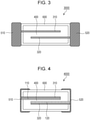
- An embodiment of the solid-state capacitor is illustrated in Fig. 3 .
- a surface-mount power storage device with high reliability is realized.
- An example of a plated device is a battery 2000 illustrated in Fig. 2 .
- the terminal electrodes have a Ni (underlying layer) and Sn (surface layer) plating applied thereto.
- the plating layers each have a thickness of greater than or equal to 1 ⁇ m and less than or equal to 5 ⁇ m.
- a total thickness of the Ni layer and the Sn layer may be, for example, greater than or equal to 1 ⁇ m and less than or equal to 10 ⁇ m.
- the solid electrolyte material having a garnet structure of the first embodiment can be manufactured by using the following method, for example.
- a Li 2 CO 3 powder, a Pr 6 O 11 powder, and a ZrO 2 powder which are starting raw materials, are prepared. Subsequently, each of the raw material powders is weighed out such that the solid electrolyte layer has a desired composition, which is, for example, a composition of Li 7 Pr 3 Zr 2 O 12 .
- a Pr-containing pyrochlore oxide e.g., Pr 2 Zr 2 O 7
- this precursor may be used as a starting raw material. In this case, too, a garnet structure can be obtained in sintering.
- compositional ratio between the three components may not necessarily be based on a stoichiometric composition. It is sufficient that the composition enables the formation of a solid solution having a cubic system garnet structure and dense sintering (e.g., a density of 4.0 g/cm 3 or greater).
- a composition in which the positions of Pr and Zr are partially replaced with a different element may be used, or an additive may be included, to produce a similar effect, provided that the different element or the additive enables the formation of a dense sintered body (e.g., a density of 4.0 g/cm 3 or greater) that is a solid solution having a cubic system garnet structure.
- a different element e.g., a rare earth metal, such as La, Nd, or Sm, or Al, Nb, Ta, Bi, or the like
- an additive may be included, to produce a similar effect, provided that the different element or the additive enables the formation of a dense sintered body (e.g., a density of 4.0 g/cm 3 or greater) that is a solid solution having a cubic system garnet structure.
- the starting raw material powders are loaded into a polyethylene ball mill, and stabilized zirconia balls ( ⁇ 5 mm) and pure water are added.
- the powders are mixed and milled (to an average particle diameter of 0.7 ⁇ 0.5 ⁇ m) for approximately 20 hours and subsequently dehydrated and dried.
- the dried powder is loaded into a high-purity alumina crucible, the crucible is coated with a lid, and the dried powder is calcined at approximately 750°C in air for 2 hours to 5 hours.
- the calcined powder is loaded into a polyethylene ball mill in a similar manner as that for the mixing, and stabilized zirconia balls ( ⁇ 5 mm) and pure water are added.
- the powder is milled for approximately 10 to 30 hours to an average particle diameter of 1.0 ⁇ 0.5 ⁇ m and, subsequently, sufficiently dehydrated and dried.
- the dried calcined powder is sintered, and, accordingly, the solid electrolyte layer 400 having a garnet structure is synthesized.
- the power storage device can be produced with the calcined milled powder by using a common layer stacking process.
- each of the calcined powders used as raw materials for the solid electrolyte layer 400 is weighed out as described above.
- An organic binder such as a butyral resin, a solvent primarily including butyl acetate, and a plasticizing agent, such as BBP are added, and mixing and dispersing is performed.
- the resulting slurry is passed through a mesh to remove aggregated powder and binder lumps, and subsequently, the resultant is shaped on a PET film of 50 ⁇ m by using a doctor blade method. In this manner, a green sheet is prepared.
- positive and negative electrode active material layers are formed from first and second active material paces on the green sheet by using a screen printing method.
- print components that constitute current collectors 300 are similarly formed by printing, from an internal electrode paste, on the active material layers. Subsequently, green sheets on which print components have been formed are stacked such that a desired configuration is achieved, and pressure is applied to the stacked green sheets. Accordingly, a stacked structure is obtained. The stacked structure is diced into separate pieces having desired dimensions, which form individual green chip devices. The green chip devices are placed in a heat-resistant alumina sagger.
- zirconia powder (average particle size of 50 ⁇ m) is uniformly spread on the bottom, and a calcined powder having the same composition as that of the green body, which is to be sintered, is spread on the zirconia powder. Thereafter, the green body is placed thereon and embedded in the calcined powder having the same composition. Heating is performed at approximately 400°C to 500°C for 2 hours to 5 hours under a nitrogen flow. In this manner, debindering is carried out.
- a sagger cover polished with 800-grit sandpaper to have a smooth surface is placed to hermetically seal the sagger, and sintering is performed at a temperature of 1050°C to 1130°C for 2 hours to 10 hours. Thereafter, the sagger cover is removed, and a heat treatment is performed at the same temperature as the sintering temperature for 5 minutes to 30 minutes. This treatment enables Li to be selectively vaporized, and, accordingly, the coating layer 600 can be formed in a surface layer region of the solid electrolyte layer 400. Subsequently, chamfering is performed by tumble polishing, and thereafter, a paste that forms the external electrodes is applied to both end surfaces of the resulting sintered body.
- the paste includes conductor particles that include at least one glass frit in an amount of 0.5 wt% to 10 wt%, and the glass frit has a softening point less than or equal to the heat treatment temperature.
- a heat treatment is performed at a temperature of 500°C to 850°C in air. Accordingly, a sintered device that forms a power storage device of the present invention is obtained.
- the heat treatment may be performed in an air atmosphere in instances in which the internal electrodes are formed of a metal that does not oxidize in air, and examples of the metal include AgPd (silver-palladium) systems.
- the metal is a non-noble metal that oxidizes in air, such as Ni or Cu
- the heat treatment is to be performed in nitrogen or the like, at an oxygen concentration at which the internal electrodes do not oxidize.
- a plating is applied to the terminal electrodes by barrel plating or the like. Application of a plating is a common practice for terminal electrodes of chip components. In this manner, a power storage device 2000, illustrated in Fig. 2 , can be obtained.
- the first active material and the second active material may each be an active material capable of charging and discharging, and a solid electrolyte may be included as a component of a mixture.
- the solid electrolyte used in the mixture is not limited to a solid electrolyte having a garnet structure. Any solid electrolyte that does not cause structural defects or unnecessary reactions in the simultaneous sintering may be used.
- the power storage device can be produced by using the same configuration as that of a common multilayer capacitor and simultaneously sintering internal electrodes that serve as current collectors; in this instance, an active material layer as described above is not formed.
- Fig. 2 is a schematic diagram illustrating a configuration of a power storage device according to a second embodiment.
- Fig. 2 is a cross-sectional view of a power storage device 2000, according to the present embodiment.
- Elements of the power storage device 2000 of the present embodiment that are common with those of the power storage device 1000 of the first embodiment are designated with the same reference numerals, and descriptions thereof may be omitted. That is, regarding the embodiments provided below, the description of one embodiment may apply to another embodiment as long as there is no technical inconsistency. Furthermore, any combination of the embodiments is possible as long as there is no technical inconsistency.
- the power storage device 2000 additionally includes a plating that coats a surface of a first external electrode 510 and a second external electrode 520. As illustrated in Fig. 2 , the power storage device 2000 includes a first plating layer 710 on the first external electrode 510 and includes a second plating layer 720 on the second external electrode 520.
- the plating layers may include two or more layers that include an underlying layer. Examples of a metal that forms the underlying layer of the plating layers include Cu, Ni, Ag, Pd, Sn, Au, and alloys of any of the foregoing metals. These may be used alone or in a combination of two or more. Examples of the underlying layer of the plating layers may include Ni and Ni alloys.
- examples of a surface layer of the plating layers include Cu, Ni, Ag, Au, Sn, Zn, and alloys of any of the foregoing metals. These may be used alone or in a combination of two or more. Examples of the surface layer of the plating layers may include Sn and Sn alloys.
- the plating layers may include, for example, Ni (underlying layer) and Sn (surface layer). A method for the plating is not particularly limited and may be a known method.
- a surface-mount power storage device having terminal electrodes that have undergone a plating process is realized.
- the plating process is achieved without causing the plating to be unnecessarily deposited on regions other than the terminal electrodes.
- Fig. 3 is a schematic diagram illustrating a configuration of a power storage device according to a third embodiment.
- Fig. 3 is a cross-sectional view of a power storage device 3000, according to the present embodiment.
- Elements of the power storage device 3000 of the present embodiment that are common with those of the power storage device 1000 of the first embodiment are designated with the same reference numerals, and descriptions thereof may be omitted. That is, regarding the embodiments provided below, the description of one embodiment may apply to another embodiment as long as there is no technical inconsistency. Furthermore, any combination of the embodiments is possible as long as there is no technical inconsistency.
- the power storage device 3000 of the present embodiment can be employed as a capacitor.
- the power storage device 3000 does not include active material layers, such as the first active material layer 110 or the second active material layer 120.
- plating handling can be performed on the terminal electrodes without causing the plating to be unnecessarily deposited on regions other than the terminal electrodes. Hence, a surface-mount power storage device is realized.
- Fig. 4 is a schematic diagram illustrating a configuration of a power storage device according to a fourth embodiment.
- Fig. 4 is a cross-sectional view of a power storage device 4000, according to the present embodiment.
- Elements of the power storage device 4000 of the present embodiment that are common with those of the power storage device 1000 of the first embodiment are designated with the same reference numerals, and descriptions thereof may be omitted. That is, regarding the embodiments provided below, the description of one embodiment may apply to another embodiment as long as there is no technical inconsistency. Furthermore, any combination of the embodiments is possible as long as there is no technical inconsistency.
- the power storage device 400 has a shape such that the first external electrode 510 and the second external electrode 520 cover a part of a peripheral part of the solid electrolyte layer 400.
- a shape of the first external electrode 510 is not particularly limited provided that the first external electrode 510 is electrically connected to the first active material layer 110 and the first internal electrode 310.
- a shape of the second external electrode 520 is not particularly limited provided that the second external electrode 520 is electrically connected to the second active material layer 120 and the second internal electrode 320.
- plating handling can be performed on the terminal electrodes without causing the plating to be unnecessarily deposited on regions other than the terminal electrodes. Hence, a surface-mount power storage device is realized.
- Fig. 5 is a schematic diagram illustrating a configuration of a power storage device according to a fifth embodiment.
- Fig. 5 is a cross-sectional view of a power storage device 5000, according to the present embodiment.
- Elements of the power storage device 5000 of the present embodiment that are common with those of the power storage device 1000 of the first embodiment are designated with the same reference numerals, and descriptions thereof may be omitted. That is, regarding the embodiments provided below, the description of one embodiment may apply to another embodiment as long as there is no technical inconsistency. Furthermore, any combination of the embodiments is possible as long as there is no technical inconsistency.
- the power storage device 5000 includes a plurality of cells.
- the power storage device 5000 includes a plurality of cells that are electrically connected to one another in parallel.
- Each of the plurality of cells includes a first active material layer 110; a second active material layer 120; a first internal electrode 310, which is electrically connected to the first active material layer 110; a second internal electrode 320, which is electrically connected to the second active material layer 120; and a solid electrolyte layer 400.
- Each of the plurality of cells has two sets of a pair of end surfaces that face each other.
- the power storage device 5000 is formed of a plurality of cells 30 that are stacked on top of one another.
- plating handling can be performed on the terminal electrodes without causing the plating to be unnecessarily deposited on regions other than the terminal electrodes. Hence, a surface-mount power storage device is realized.
- Fig. 6 is a schematic diagram illustrating a configuration of a power storage device according to a sixth embodiment.
- Fig. 6 is a cross-sectional view of a power storage device 6000, according to the present embodiment.
- Elements of the power storage device 6000 of the present embodiment that are common with those of the power storage device 1000 of the first embodiment are designated with the same reference numerals, and descriptions thereof may be omitted. That is, regarding the embodiments provided below, the description of one embodiment may apply to another embodiment as long as there is no technical inconsistency. Furthermore, any combination of the embodiments is possible as long as there is no technical inconsistency.
- the first active material layer 110 is not in contact with the first external electrode 510. That is, in the power storage device 6000, the first active material layer 110 is disposed inside the solid electrolyte layer 400 and on the first internal electrode 310 while being physically separated from the first external electrode 510. Furthermore, in the power storage device 6000, the second active material layer 120 is not in contact with the second external electrode 520. That is, in the power storage device 6000, the second active material layer 120 is disposed inside the solid electrolyte layer 400 and on the second internal electrode 320 while being physically separated from the second external electrode 520.
- a shape of the first external electrode 510 is not particularly limited provided that the first external electrode 510 is electrically connected to the first internal electrode 310.
- a shape of the second external electrode 520 is not particularly limited provided that the second external electrode 520 is electrically connected to the second internal electrode 320.
- Fig. 7 is a schematic diagram illustrating a configuration of a power storage device according to a seventh embodiment.
- Fig. 7 is a cross-sectional view of a power storage device 7000, according to the present embodiment.
- Elements of the power storage device 7000 of the present embodiment that are common with those of the power storage device 1000 of the first embodiment are designated with the same reference numerals, and descriptions thereof may be omitted. That is, regarding the embodiments provided below, the description of one embodiment may apply to another embodiment as long as there is no technical inconsistency. Furthermore, any combination of the embodiments is possible as long as there is no technical inconsistency.
- the power storage device 7000 additionally includes resin electrodes that coat a surface of the first external electrode 510 and a surface of the second external electrode 520. As illustrated in Fig. 7 , the power storage device 7000 additionally includes a first resin electrode 810 on a surface of the first external electrode 510 and additionally includes a second resin electrode 820 on a surface of the second external electrode 520.
- the first resin electrode 810 and the second resin electrode 820 may have a Young's modulus less than a Young's modulus of the first external electrode 510 and a Young's modulus of the second external electrode 520.
- the first resin electrode 810 and the second resin electrode 820 may be a conductive resin.
- a material that is included in the conductive resin is not particularly limited and may be a known material.
- a method for forming the first resin electrode 810 and the second resin electrode 820 is not particularly limited and may be a known method.
- the power storage device 7000 may include a plating layer on surfaces of the first external electrode 510 and the second external electrode 520 or on surfaces of the first resin electrode 810 and the second resin electrode 820.
- Batteries of the present disclosure which use a solid electrolyte, are useful as a power storage device that is used in various electronic or electrical devices.
Landscapes
- Chemical & Material Sciences (AREA)
- Engineering & Computer Science (AREA)
- Chemical Kinetics & Catalysis (AREA)
- Electrochemistry (AREA)
- General Chemical & Material Sciences (AREA)
- Power Engineering (AREA)
- Manufacturing & Machinery (AREA)
- Inorganic Chemistry (AREA)
- Microelectronics & Electronic Packaging (AREA)
- Materials Engineering (AREA)
- Physics & Mathematics (AREA)
- Condensed Matter Physics & Semiconductors (AREA)
- General Physics & Mathematics (AREA)
- Ceramic Engineering (AREA)
- Secondary Cells (AREA)
- Connection Of Batteries Or Terminals (AREA)
- Electric Double-Layer Capacitors Or The Like (AREA)
Abstract
Description
- The present disclosure relates to a power storage device in which a solid electrolyte is used.
- Patent Literature 1 discloses a battery in which a solid electrolyte structure made of a garnet-type crystal Li7L3Zr2O12 is included, and a surface of the structure is coated with a resin. Patent Literature 2 discloses a battery in which Li7La3Zr2O12 is used as a solid electrolyte, and an insulating layer is used between a positive electrode or a negative electrode and the solid electrolyte.
-
- PTL 1: International Publication No.
2013/100001 - PTL 2:
Japanese Unexamined Patent Application Publication No. 2017-139199 - An object of the present disclosure is to provide a surface-mount power storage device.
- The present disclosure provides a power storage device. The power storage device includes
- a solid electrolyte layer;
- a coating layer that coats a surface of the solid electrolyte layer;
- a first internal electrode disposed inside the solid electrolyte layer;
- a first external electrode disposed outside of the solid electrolyte layer and electrically connected to the first internal electrode;
- a second internal electrode disposed inside the solid electrolyte layer; and a second external electrode disposed outside of the solid electrolyte layer and electrically connected to the second internal electrode.
- The coating layer has a conductivity less than a conductivity of the solid electrolyte layer, and
the coating layer has a thickness of greater than or equal to 1 µm and less than or equal to 100 µm. - With the present disclosure, surface-mount power storage devices are provided.
-
- [
Fig. 1] Fig. 1 is a schematic cross-sectional view illustrating a configuration of a power storage device according to a first embodiment of the present disclosure. - [
Fig. 2] Fig. 2 is a schematic cross-sectional view illustrating a configuration of a power storage device according to a second embodiment of the present disclosure. - [
Fig. 3] Fig. 3 is a schematic cross-sectional view illustrating a configuration of a power storage device according to a third embodiment of the present disclosure. - [
Fig. 4] Fig. 4 is a schematic cross-sectional view illustrating a configuration of a power storage device according to a fourth embodiment of the present disclosure. - [
Fig. 5] Fig. 5 is a schematic cross-sectional view illustrating a configuration of a power storage device according to a fifth embodiment of the present disclosure. - [
Fig. 6] Fig. 6 is a schematic cross-sectional view illustrating a configuration of a power storage device according to a sixth embodiment of the present disclosure. - [
Fig. 7] Fig. 7 is a schematic cross-sectional view illustrating a configuration of a power storage device according to a seventh embodiment of the present disclosure. - According to a first aspect of the present disclosure, a power storage device includes:
- a solid electrolyte layer;
- a coating layer that coats a surface of the solid electrolyte layer;
- a first internal electrode disposed inside the solid electrolyte layer;
- a first external electrode disposed outside of the solid electrolyte layer and electrically connected to the first internal electrode;
- a second internal electrode disposed inside the solid electrolyte layer; and
- a second external electrode disposed outside of the solid electrolyte layer and electrically connected to the second internal electrode.
- The coating layer has a conductivity less than a conductivity of the solid electrolyte layer, and
the coating layer has a thickness of greater than or equal to 1 µm and less than or equal to 100 µm. - With the first aspect, an insulating property of the surface of the solid electrolyte layer is ensured. Consequently, in instances where a plating process is performed on a terminal, deposition of the plating on portions other than the terminal is inhibited. Accordingly, the power storage device provided is suitable for solder mounting.
- In a second aspect of the present disclosure, the power storage device of the first aspect may be such that, for example, the power storage device further includes an active material layer disposed inside the solid electrolyte layer. With this configuration, the power storage device provided is suitable for solder mounting.
- In a third aspect of the present disclosure, the power storage device according to the first or second aspect may be such that, for example, the solid electrolyte layer is a sintered body. With this configuration, the power storage device provided is suitable for solder mounting.
- In a fourth aspect of the present disclosure, the power storage device according to any one of the first to third aspects may be such that, for example, the solid electrolyte layer has a garnet structure. With this configuration, the power storage device provided is suitable for solder mounting.
- In a fifth aspect of the present disclosure, the power storage device according to any one of the first to fourth aspects may be such that, for example, the solid electrolyte layer contains no sulfur. With this configuration, the power storage device provided is suitable for solder mounting.
- In a sixth aspect of the present disclosure, the power storage device according to any one of the first to fifth aspects may be such that, for example, the solid electrolyte layer includes a crystalline phase including at least one selected from the group consisting of Li7La3Zr2O12 and Li7Pr3Zr2O12. With this configuration, the power storage device provided is suitable for solder mounting.
- In a seventh aspect of the present disclosure, the power storage device according to any one of the first to sixth aspects may be such that, for example, the coating layer has a conductivity of less than or equal to 10-4 S/cm. With this configuration, the power storage device provided is suitable for solder mounting.
- In an eighth aspect of the present disclosure, the power storage device according to any one of the first to seventh aspects may be such that, for example, the coating layer includes an oxide. With this configuration, the power storage device provided is suitable for solder mounting.
- In a ninth aspect of the present disclosure, the power storage device according to the eighth aspect may be such that, for example, the oxide includes a pyrochlore oxide. With this configuration, the power storage device provided is suitable for solder mounting.
- In a tenth aspect of the present disclosure, the power storage device according to the ninth aspect may be such that, for example, the pyrochlore oxide includes at least one selected from the group consisting of La2Zr2O7 and Pr2Zr2O7. With this configuration, the power storage device provided is suitable for solder mounting.
- In an eleventh aspect of the present disclosure, the power storage device according to any one of the first to tenth aspects may be such that, for example, the coating layer includes a crystalline phase including Li2ZrO3. With this configuration, the power storage device provided is suitable for solder mounting.
- In a twelfth aspect of the present disclosure, the power storage device according to any one of the first to eleventh aspects may be such that, for example, the coating layer has a Li content molar ratio less than a Li content molar ratio of the solid electrolyte layer. With this configuration, the power storage device provided is suitable for solder mounting.
- In a thirteenth aspect of the present disclosure, the power storage device according to any one of the first to twelfth aspects may be such that, for example, the coating layer has a thickness of greater than or equal to 5 µm and less than or equal to 100 µm. With this configuration, the power storage device provided is suitable for solder mounting.
- In a fourteenth aspect of the present disclosure, the power storage device according to any one of the first to thirteenth aspects may be such that, for example, the power storage device further includes a plating that coats a surface of the first external electrode and a surface of the second external electrode. With this configuration, the power storage device provided is suitable for solder mounting.
- In a fifteenth aspect of the present disclosure, the power storage device according to any one of the first to fourteenth aspects may be such that, for example, the plating has a thickness of greater than or equal to 1 µm and less than or equal to 10 µm. With this configuration, the power storage device provided is suitable for solder mounting.
- Now, embodiments will be described in detail with reference to the drawings.
- Note that each of the embodiments described below is a generic or specific example. In the following descriptions of the embodiments, the mentioned numerical values, shapes, materials, constituent elements, arrangements of the constituent elements, forms of connections thereof, and the like are merely illustrative and are not intended to limit the present disclosure. Furthermore, among the constituent elements in the following embodiments, constituent elements not described in the independent claim, which represents the most generic concept, will be described as optional constituent elements.
- Furthermore, the drawings are not necessarily drawn to scale. In the drawings, substantially identical components are assigned the same numerals, and redundant descriptions thereof will be omitted or simplified.
- First, a power storage device according to the present embodiment will be described.
- The power storage device may be an all-solid-state battery or a capacitor.
-
Fig. 1 is a cross-sectional view of apower storage device 1000, according to a first embodiment. In the present embodiment, thepower storage device 1000 is an all-solid-state battery. In the present specification, thepower storage device 1000 may be referred to as a "battery 1000". Furthermore, in the present specification, a first external electrode and a second external electrode may be collectively referred to as "terminal electrodes". Furthermore, in the present specification, a first internal electrode may be referred to as a "first current collector", and a second internal electrode may be referred to as a "second current collector". - As illustrated in
Fig. 1 , thepower storage device 1000 includes asolid electrolyte layer 400, acoating layer 600, a firstinternal electrode 310, a firstexternal electrode 510, a secondinternal electrode 320, and a secondexternal electrode 520. The firstinternal electrode 310 is disposed inside thesolid electrolyte layer 400. The firstexternal electrode 510 is disposed outside of thesolid electrolyte layer 400 and electrically connected to the firstinternal electrode 310. The secondinternal electrode 320 is disposed inside thesolid electrolyte layer 400. The secondexternal electrode 520 is disposed outside of thesolid electrolyte layer 400 and electrically connected to the secondinternal electrode 320. Thecoating layer 600 coats a surface of thesolid electrolyte layer 400. Thecoating layer 600 has a conductivity less than a conductivity of thesolid electrolyte layer 400. The conductivity of thecoating layer 600 may be one or more orders of magnitude less than the conductivity of thesolid electrolyte layer 400 and, for example, may be less than or equal to 10-4 S/cm. Thecoating layer 600 may be, for example, an insulating layer. - The
power storage device 1000 may include an active material layer disposed inside thesolid electrolyte layer 400. Thepower storage device 1000 may include an active material layer, which may be a firstactive material layer 110. The firstactive material layer 110 may be disposed inside thesolid electrolyte layer 400 and on the firstinternal electrode 310 and may be electrically connected to the firstexternal electrode 510. Furthermore, thepower storage device 1000 may include an active material layer, which may be a secondactive material layer 120. The secondactive material layer 120 may be disposed inside thesolid electrolyte layer 400 and on the secondinternal electrode 320 and may be electrically connected to the secondexternal electrode 520. The firstactive material layer 110 may be disposed to face the secondactive material layer 120 with thesolid electrolyte layer 400 disposed therebetween. - With this configuration, a plating process can be selectively performed on the terminal electrodes, without causing the plating to be unnecessarily deposited on regions other than the terminal electrodes. Accordingly, a basic configuration of a surface-mount power storage device is realized.
- The
solid electrolyte layer 400 is, for example, a sintered body. Examples of a material of thesolid electrolyte layer 400 include materials having a crystal structure of a garnet structure, materials having a crystal structure that has a NASICON-type structure, and materials having a perovskite-type crystal structure. For example, thesolid electrolyte layer 400 is a material having a crystal structure of a garnet structure. For example, thesolid electrolyte layer 400 is a sulfur-free material. For example, thesolid electrolyte layer 400 may include a crystalline phase including Li7La3Zr2O12 or Li7Pr3Zr2O12. - With any of the configurations described above, an insulating property of the surface of the solid electrolyte layer is ensured. Accordingly, plating handling can be performed on the terminal electrodes without causing the plating to be unnecessarily deposited on regions other than the terminal electrodes. Hence, a surface-mount power storage device is realized.
- The
coating layer 600 may include an oxide, for example. The oxide may include a pyrochlore oxide, for example. The pyrochlore oxide may include La2Zr2O7 or Pr2Zr2O7, for example. Thecoating layer 600 may include a crystalline phase including Li2ZrO3, for example. Thecoating layer 600 may have a Li content molar ratio less than a Li content molar ratio of thesolid electrolyte layer 400. - The
coating layer 600 has a thickness of greater than or equal to 1 µm and less than or equal to 100 µm. If the thickness of thecoating layer 600 is less than 1 µm, the coating layer dissolves into a plating liquid during the formation of the plating layer on the terminal electrode, and as a result, the insulating property of the surface of the solid electrolyte layer is not ensured. Furthermore, moisture can easily penetrate the surface of the solid electrolyte layer, that is, moisture resistance is degraded. If the thickness of thecoating layer 600 is greater than 100 µm, cracking or peeling of the coating layer occurs due to a cooling-heating cycle or handling, and as a result, the insulating property of the surface of the solid electrolyte layer is not ensured. The thickness of thecoating layer 600 may be greater than or equal to 5 µm and less than or equal to 100 µm, for example. When the thickness of thecoating layer 600 is greater than or equal to 5 µm, a sintered device can be tumble-polished while the coating layer is retained thereon. Accordingly, smoothing of a surface of the sintered device and chamfering of the four corners and edges can be accomplished, and, consequently, improvement in flexural strength and inhibition of chipping in the sintered device are realized. - Furthermore, the constituent elements of the
coating layer 600 may be similar to those of thesolid electrolyte layer 400. Furthermore, thesolid electrolyte layer 400 andcoating layer 600 may both be an oxide. Specifically, thesolid electrolyte layer 400 may include a crystalline phase including Li7La3Zr2O12 or Li7Pr3Zr2O12, and thecoating layer 600 may include an oxide of thesolid electrolyte layer 400. In this instance, the oxide of thesolid electrolyte layer 400 may include at least one of a pyrochlore oxide (e.g., La2Zr2O7 or Pr2Zr2O7) or Li2ZrO3. In such instances, joining interfaces of thesolid electrolyte layer 400 and thecoating layer 600 have similar coefficients of thermal expansion and therefore have a high degree of matching; hence, high thermal shock resistance is achieved compared insidestances in which a solid electrolyte is coated with a resin or a glass. Consequently, in solder mounting, the occurrence of cracking at the interfaces is inhibited, and excellent thermal resistance is exhibited. Accordingly, suitability for surface mounting is achieved. The "thermal resistance" refers to durability against the heat treatment in the so-called solder reflow. Furthermore, in actual usage, excellent thermal stress, such as a cooling-heating cycle, is exhibited. As a result of these advantageous effects, suitability for surface mounting and high reliability are realized. - In instances where the
solid electrolyte layer 400 includes a crystalline phase including Li7La3Zr2O12 or Li7Pr3Zr2O12, sintering or heat treatment of an unsintered, green device of thesolid electrolyte layer 400 results in the formation of acoating layer 600 including a pyrochlore oxide. Consequently, thesolid electrolyte layer 400 and thecoating layer 600 are formed with a mutually diffused continuous joining interface without a gap. Accordingly, high joining strength is achieved because of the strong bond due to a sintered structure, compared with sintered devices having a resin coating on the surface. As a result of this advantageous effect, high environmental resistance is achieved without causing problems, such as a problem with a plating liquid or moisture penetrating the joining interface. - With any of the configurations described above, a plating process can be performed on the terminal electrodes without causing the plating to be unnecessarily deposited on regions other than the terminal electrodes. Consequently, a power storage device, as illustrated in
Fig. 2 , that is suitable for surface mounting and has excellent environmental resistance, such as resistance to impact and thermal shock, is realized. - Note that the
coating layer 600 may include a crystalline phase including Li2ZrO3, which has a conductivity less than a conductivity of a crystalline phase having a garnet structure. In this case, the formedcoating layer 600 has high adhesion to thesolid electrolyte layer 400, that is, the obtainedcoating layer 600 has excellent environmental resistance, such as resistance to impact and thermal shock. Furthermore, the Li content molar ratio in thecoating layer 600 may be less than the Li content molar ratio in thesolid electrolyte layer 400. When the Li content molar ratio in thecoating layer 600 is less than the Li content molar ratio in thesolid electrolyte layer 400, thecoating layer 600 has reduced conductivity because of the reduction in carriers. As a result, thecoating layer 600 has the same effects as the effects described above. - With any of the configurations described above, a plating process can be performed on the terminal electrodes without causing the plating to be unnecessarily deposited on regions other than the terminal electrodes. Hence, a surface-mount power storage device is realized.
- In the present embodiment, the "sintered device" is defined, for example, as a device formed of a combination of the sintered body of the
solid electrolyte layer 400, the firstinternal electrode 310 and the secondinternal electrode 320, which are included as current collectors inside the sintered body, and thecoating layer 600. - For example, the sintered device is formed of a solid solution composition and the
coating layer 600, which coats a surface thereof, and the solid solution composition has a garnet structure including Li7La3Zr2O12 or Li7Pr3Zr2O12. - The
solid electrolyte layer 400 of the first embodiment is an oxide-based solid electrolyte and, therefore, unlike a sulfur-based solid electrolyte, may not contain sulfur. Accordingly, the sintered device formed from a solid electrolyte material of the first embodiment does not generate hydrogen sulfide when exposed to air or moisture and, therefore, provides high stability. Hence, the sintered device can be employed in a power storage device that can be produced and used in air. Furthermore, the sintered device can be used even after being impregnated with a plating liquid. It is sufficient that the crystalline phase present in thesolid electrolyte layer 400 of the first embodiment have a garnet-type crystal structure. The crystalline phase may have a cubic system, which is dense and has high conductivity. Furthermore, the crystalline phase may have a tetragonal system. - Furthermore, in the
solid electrolyte layer 400 of the first embodiment, the solid electrolyte layer having a garnet structure may contain an element different from La or Pr, so that some objects can be achieved. One of the objects is to improve density of thesolid electrolyte layer 400. Another of the objects is to realize integrated sintering of a stacked structure that may include the first current collector and the second current collector, for instance. Another of the objects is to adjust a shrinkage property with respect to a sintering temperature. Examples of the different element include elements such as Al, Nb, Ta, and Bi and rare earth metals such as La, Nd, and Sm. - Furthermore, the
solid electrolyte layer 400 may include a crystalline phase having a crystal structure different from a garnet-type crystal structure, provided that conductivity and air stability are not compromised. For example, thesolid electrolyte layer 400 may include a pyrochlore phase (e.g., Pr2Zr2O7), which has high air stability, and/or the like. Note that the crystal structures present therein can be identified from an X-ray diffraction pattern of a cross section of a sample. Since a volume fraction of thecoating layer 600 is small in the entirety of the sintered device, a diffraction pattern of the entirety of a cross section is sufficient for determining the crystalline phase. In a case where a more precise determination is desired, using an XRD pattern of a local region or a diffraction pattern of a sample from which thecoating layer 600 has been removed is effective. - Furthermore, a conductive additive may be included in the
solid electrolyte layer 400 to increase electron conductivity. Examples of the conductive additive include graphites, such as natural graphite and artificial graphite; carbon blacks, such as acetylene black and Ketjen black; conductive fibers, such as carbon fibers and metal fibers; carbon fluoride; metal powders, such as aluminum powders; conductive whiskers, such as zinc oxide whiskers and potassium titanate whiskers; conductive metal oxides, such as titanium oxide; and conductive polymer compounds, such as polyaniline, polypyrrole, and polythiophene. - The
coating layer 600 coats the surface of the sintered body of thesolid electrolyte layer 400, which is primarily formed of a garnet structure, except that thecoating layer 600 does not coat end portions (end surfaces connected to the terminal electrodes) of the firstinternal electrode 310 and the secondinternal electrode 320, which are current collectors. Thecoating layer 600 is, for example, an oxide having a pyrochlore structure, which has a conductivity less than the conductivity of thesolid electrolyte layer 400. Specifically, thecoating layer 600 may include La2Zr2O7 or Pr2Zr2O7. - The pyrochlore oxide, which forms the
coating layer 600, has low conductivity. The present inventors discovered that Li2ZrO3, which, when thesolid electrolyte layer 400 primarily formed of a garnet structure is over-sintered, is deposited on a surface portion thereof, has also high air stability and low conductivity. Accordingly, in instances where thecoating layer 600 includes a pyrochlore oxide and Li2ZrO3, thecoating layer 600 produces enhanced advantageous effects. For example, thecoating layer 600 has an advantageous effect of not causing a plating to be unnecessarily deposited on regions other than the terminal electrodes. - The sintered device is dense (a density > 4.0 g/cm3) and stable to air and moisture and, therefore, exhibits high durability even when a plating liquid is impregnated and when devices collide with each other in the manufacturing process.
- The
coating layer 600 may contain an element different from La or Pr. Examples of the different element include elements such as Al, Nb, Ta, and Bi and rare earth metals such as La, Nd, and Sm; these elements can be easily incorporated into the garnet structure or the pyrochlore structure. - Furthermore, the molar ratio of the Li element content in the
coating layer 600 may be less than the Li content molar ratio in the solid electrolyte layer. That is, in a case where the conductive carriers (Li ions) distributed in a surface layer are vaporized by using a sintering process condition or a heat treatment, and the conductive carriers are thus reduced compared with an inner portion, even a garnet structure can form thecoating layer 600. - Note that in the related art, it is common to inhibit the vaporization of Li during the sintering of a
solid electrolyte layer 400. In contrast, thecoating layer 600 of the present disclosure is obtained, for example, by selectively vaporizing Li during the over-sintering of thesolid electrolyte layer 400, thereby forming an oxide in a surface layer region of thesolid electrolyte layer 400. - As with the
solid electrolyte layer 400, the crystal structures in thecoating layer 600 can also be identified from an XRD pattern of a sample, which is a sample of a local region or a sample processed to include only a high-resistance layer. Note that the pyrochlore oxide is formed in the surface layer by selectively vaporizing Li from the surface layer in the process of sintering the solid solution composition having a garnet structure. For example, a pyrochlore oxide can be formed exclusively in the surface layer region by heat-treating the sintered body of a solid electrolyte having a garnet structure at a temperature of 700°C to 1300°C for 10 minutes to 60 minutes in air. In this manner, a power storage device in which thecoating layer 600, which has a thickness of greater than or equal to 1 µm and less than or equal to 100 µm and is stable, is integrated with thesolid electrolyte layer 400, is realized. With such a method, thecoating layer 600 can be formed to have a large thickness and extend over a wide area. Note that the thickness of thecoating layer 600 can be controlled by the temperature or by a process time, that is, thecoating layer 600 can be formed to have a large thickness by using a high temperature or extending the process time. Furthermore, in the process of forming the coating layer, a highly permeable, heat-resistant container may be used. For example, a heat-resistant container having a surface with irregularities may be used. In this case, thecoating layer 600 can be formed to have a more uniform thickness. The heat-resistant container may be an alumina container having a porosity of greater than or equal to 30% and less than or equal to 60%, so as to provide higher permeability. Furthermore, the surface with irregularities may be an embossed surface with projections of approximately 50 µm. - Note that for ceramic chip components, typically, a chamfering process is performed on a sintered device to prevent chipping or improve mechanical strength. The chamfering process may be performed by tumble-polishing or the like provided that the
coating layer 600 can be retained, and subsequently, the terminal electrodes may be formed and subjected to a plating process. Accordingly, the thickness of thecoating layer 600 may be, for example, greater than or equal to 5 µm. Note that, to completely prevent the penetration of a plating liquid into the sintered device, a liquid repellent agent, such as a silane coupling agent, may be applied prior to plating. - With any of the configurations described above, a state is realized in which the surface of the solid electrolyte sintered device is coated with the
coating layer 600, which has high impact resistance and environmental resistance. The thickness of thecoating layer 600 can be evaluated by observing a cross section thereof with an optical microscope or an SEM. For example, an average of thicknesses at randomly selected five points of the cross section may be employed as the thickness of thecoating layer 600. Furthermore, the conductivity of thecoating layer 600 and the interior of the sintered body can be measured by surface resistance measurement (a 4-point probe measurement method, for example, with a Loresta-GX, manufactured by Mitsubishi Chemical Analytech Co.). Alternatively, the evaluation can be made by using a nano-probing system (Hitachi, Ltd.), which can be used for failure analysis of a semiconductor device, such as an LSI. - The first
internal electrode 310 and the secondinternal electrode 320 are internal layer current collectors of the sintered device, and a metal having high conductivity may be used in these electrodes. For example, a metal such as Pd, Pt, Ag, Cu, or Ni, an alloy such as Ag-Pd or Ag-Pt, or the like may be used. A metal that enables the firstinternal electrode 310 and the secondinternal electrode 320 to have a melting point greater than or equal to a sintering temperature of thesolid electrolyte layer 400 may be used so that the electrodes and thesolid electrolyte layer 400 can be simultaneously sintered. Note that in instances where a non-noble metal, such as Cu or Ni, is used, the sintering is to be performed at a controlled oxygen partial pressure at which the electrodes do not oxidize; in this manner, the metal can be used as an internal electrode that serves as a current collector. Furthermore, a sintering shrinkage factor may be controlled. This is to address a problem in which, in the sintering process, a difference in a shrinkage property causes the electrode metal to peel off from the interface formed with a portion surrounding the electrode metal. In addition, an additive that can be diffused into the surrounding portion for binding may be included to an extent that does not impair conductivity. Additives that may be included in such an electrode material include binding solid electrolytes and positive and negative electrode active materials. Any of a variety of metals, oxides, and the like may be used. These additives may have a particle diameter of less than or equal to a thickness of the electrodes. - The terminal electrodes are formed of a metal that exhibits high conductivity. Specific examples thereof include Ag, Cu, Ni, Pt, Pd, Ag-Pd, and Ag-Pt. Typically, the terminal electrodes are formed by applying a metal powder paste to end surfaces of the sintered body and heat-treating the metal powder paste. Accordingly, an electrical connection with the internal electrodes, which serve as current collectors, is ensured.
- To increase the joining strength achieved with the sintered body, a glass frit may be included and diffused into the sintered device, and, consequently, terminal electrodes having high bonding strength can be formed. Furthermore, an effect of clogging pores in the heat-treated electrode structures with a glass component is produced and, accordingly, a sealing effect is also produced for preventing moisture of, for example, a plating liquid from penetrating into the interior of the sintered device and thus degrading properties. When such a glass component included in the terminal electrodes is heat-treated at a temperature greater than or equal to the melting point thereof, the glass component wets and spreads on the irregularities and in open pores of the surface of the
coating layer 600 under capillary action and clogs penetration paths or pores of thecoating layer 600. Accordingly, a sealing effect for the entirety of the sintered device can also be produced. If the glass component is directly diffused into the solid electrolyte layer, the glass component travels along the grain boundaries, at which a diffusion rate is high, and, therefore, rapidly diffuses inside the sintered body and blocks a conduction path; as a result, conductivity may be degraded. Accordingly, thecoating layer 600 may be used as a diffusion layer for a glass frit, that is, as a protective layer for thesolid electrolyte layer 400. In this case, degradation of conductivity in a functional portion is inhibited. With these advantageous effects, a high-performance power storage device can be obtained which has high reliability as exhibited in, for instance, flexural stress, drop impact, and/or environmental resistance tests after the device is mounted to a substrate. The "functional portion" is, for example, a region between a positive electrode and a negative electrode. Examples of the environmental resistance test include a test for examining durability against moisture. - In the
power storage device 1000, the firstactive material layer 110 may be used as a positive electrode, for example. The firstactive material layer 110 that is used as a positive electrode includes a material having a property of occluding and releasing metal ions. Examples of the metal ions include lithium ions. The positive electrode includes a positive electrode active material, for example. The positive electrode may include asolid electrolyte layer 400. This is effective for forming a conduction path, and in addition, correcting structural defects and/or controlling a sintering shrinkage factor in an instance in which the positive electrode active material and thesolid electrolyte layer 400 are simultaneously sintered. Resulting effects that can be provided are a high energy density and a high discharge capacity. - In the
power storage device 1000, the secondactive material layer 120 may be used as a negative electrode, for example. The secondactive material layer 120 that is used as a negative electrode includes a material having a property of occluding and releasing metal ions. Examples of the metal ions include lithium ions. For example, the negative electrode includes a negative electrode active material and may include a solid electrolyte; this is effective for correcting structural defects and/or controlling a sintering shrinkage factor in an instance in which the negative electrode active material and the solid electrolyte are simultaneously sintered. Accordingly, a similar effect to that of the positive electrode is produced. - Note that a conductive additive may be included in at least one selected from the positive electrode and the negative electrode to increase electron conductivity.
- Note that in instances where neither the first active material layer 100 nor the second active material layer 200 is formed on the current collector, the resulting device may be a device that can serve as a solid-state capacitor. An embodiment of the solid-state capacitor is illustrated in
Fig. 3 . - With any of the configurations described above, a surface-mount power storage device with high reliability is realized. An example of a plated device is a
battery 2000 illustrated inFig. 2 . For example, the terminal electrodes have a Ni (underlying layer) and Sn (surface layer) plating applied thereto. The plating layers each have a thickness of greater than or equal to 1 µm and less than or equal to 5 µm. A total thickness of the Ni layer and the Sn layer may be, for example, greater than or equal to 1 µm and less than or equal to 10 µm. - The solid electrolyte material having a garnet structure of the first embodiment can be manufactured by using the following method, for example.
- First, a Li2CO3 powder, a Pr6O11 powder, and a ZrO2 powder, which are starting raw materials, are prepared. Subsequently, each of the raw material powders is weighed out such that the solid electrolyte layer has a desired composition, which is, for example, a composition of Li7Pr3Zr2O12. Note that a Pr-containing pyrochlore oxide (e.g., Pr2Zr2O7), which is an intermediate phase and is formed as a result of calcination, may be synthesized in advance, and this precursor may be used as a starting raw material. In this case, too, a garnet structure can be obtained in sintering. Furthermore, the compositional ratio between the three components may not necessarily be based on a stoichiometric composition. It is sufficient that the composition enables the formation of a solid solution having a cubic system garnet structure and dense sintering (e.g., a density of 4.0 g/cm3 or greater).
- In the garnet structure, a composition in which the positions of Pr and Zr are partially replaced with a different element (e.g., a rare earth metal, such as La, Nd, or Sm, or Al, Nb, Ta, Bi, or the like) may be used, or an additive may be included, to produce a similar effect, provided that the different element or the additive enables the formation of a dense sintered body (e.g., a density of 4.0 g/cm3 or greater) that is a solid solution having a cubic system garnet structure.
- Next, the starting raw material powders are loaded into a polyethylene ball mill, and stabilized zirconia balls (ϕ 5 mm) and pure water are added. The powders are mixed and milled (to an average particle diameter of 0.7 ± 0.5 µm) for approximately 20 hours and subsequently dehydrated and dried. The dried powder is loaded into a high-purity alumina crucible, the crucible is coated with a lid, and the dried powder is calcined at approximately 750°C in air for 2 hours to 5 hours. Next, the calcined powder is loaded into a polyethylene ball mill in a similar manner as that for the mixing, and stabilized zirconia balls (ϕ 5 mm) and pure water are added. The powder is milled for approximately 10 to 30 hours to an average particle diameter of 1.0 ± 0.5 µm and, subsequently, sufficiently dehydrated and dried. The dried calcined powder is sintered, and, accordingly, the
solid electrolyte layer 400 having a garnet structure is synthesized. The power storage device can be produced with the calcined milled powder by using a common layer stacking process. - Now, a method for manufacturing the power storage device of the present embodiment will be described in detail.
- First, each of the calcined powders used as raw materials for the
solid electrolyte layer 400 is weighed out as described above. An organic binder, such as a butyral resin, a solvent primarily including butyl acetate, and a plasticizing agent, such as BBP are added, and mixing and dispersing is performed. The resulting slurry is passed through a mesh to remove aggregated powder and binder lumps, and subsequently, the resultant is shaped on a PET film of 50 µm by using a doctor blade method. In this manner, a green sheet is prepared. Next, positive and negative electrode active material layers are formed from first and second active material paces on the green sheet by using a screen printing method. Furthermore, print components that constitute current collectors 300 are similarly formed by printing, from an internal electrode paste, on the active material layers. Subsequently, green sheets on which print components have been formed are stacked such that a desired configuration is achieved, and pressure is applied to the stacked green sheets. Accordingly, a stacked structure is obtained. The stacked structure is diced into separate pieces having desired dimensions, which form individual green chip devices. The green chip devices are placed in a heat-resistant alumina sagger. To prevent the green body from coming in direct contact with the bottom of the sagger, zirconia powder (average particle size of 50 µm) is uniformly spread on the bottom, and a calcined powder having the same composition as that of the green body, which is to be sintered, is spread on the zirconia powder. Thereafter, the green body is placed thereon and embedded in the calcined powder having the same composition. Heating is performed at approximately 400°C to 500°C for 2 hours to 5 hours under a nitrogen flow. In this manner, debindering is carried out. Thereafter, a sagger cover polished with 800-grit sandpaper to have a smooth surface is placed to hermetically seal the sagger, and sintering is performed at a temperature of 1050°C to 1130°C for 2 hours to 10 hours. Thereafter, the sagger cover is removed, and a heat treatment is performed at the same temperature as the sintering temperature for 5 minutes to 30 minutes. This treatment enables Li to be selectively vaporized, and, accordingly, thecoating layer 600 can be formed in a surface layer region of thesolid electrolyte layer 400. Subsequently, chamfering is performed by tumble polishing, and thereafter, a paste that forms the external electrodes is applied to both end surfaces of the resulting sintered body. The paste includes conductor particles that include at least one glass frit in an amount of 0.5 wt% to 10 wt%, and the glass frit has a softening point less than or equal to the heat treatment temperature. After the paste is dried, a heat treatment is performed at a temperature of 500°C to 850°C in air. Accordingly, a sintered device that forms a power storage device of the present invention is obtained. Note that the heat treatment may be performed in an air atmosphere in instances in which the internal electrodes are formed of a metal that does not oxidize in air, and examples of the metal include AgPd (silver-palladium) systems. In instances where the metal is a non-noble metal that oxidizes in air, such as Ni or Cu, the heat treatment is to be performed in nitrogen or the like, at an oxygen concentration at which the internal electrodes do not oxidize. Subsequently, a plating is applied to the terminal electrodes by barrel plating or the like. Application of a plating is a common practice for terminal electrodes of chip components. In this manner, apower storage device 2000, illustrated inFig. 2 , can be obtained. - Note that the first active material and the second active material may each be an active material capable of charging and discharging, and a solid electrolyte may be included as a component of a mixture. The solid electrolyte used in the mixture is not limited to a solid electrolyte having a garnet structure. Any solid electrolyte that does not cause structural defects or unnecessary reactions in the simultaneous sintering may be used. Furthermore, in an instance where the power storage device is employed as a solid-state ion capacitor, the power storage device can be produced by using the same configuration as that of a common multilayer capacitor and simultaneously sintering internal electrodes that serve as current collectors; in this instance, an active material layer as described above is not formed.
-
Fig. 2 is a schematic diagram illustrating a configuration of a power storage device according to a second embodiment.Fig. 2 is a cross-sectional view of apower storage device 2000, according to the present embodiment. Elements of thepower storage device 2000 of the present embodiment that are common with those of thepower storage device 1000 of the first embodiment are designated with the same reference numerals, and descriptions thereof may be omitted. That is, regarding the embodiments provided below, the description of one embodiment may apply to another embodiment as long as there is no technical inconsistency. Furthermore, any combination of the embodiments is possible as long as there is no technical inconsistency. - The
power storage device 2000 additionally includes a plating that coats a surface of a firstexternal electrode 510 and a secondexternal electrode 520. As illustrated inFig. 2 , thepower storage device 2000 includes afirst plating layer 710 on the firstexternal electrode 510 and includes asecond plating layer 720 on the secondexternal electrode 520. The plating layers may include two or more layers that include an underlying layer. Examples of a metal that forms the underlying layer of the plating layers include Cu, Ni, Ag, Pd, Sn, Au, and alloys of any of the foregoing metals. These may be used alone or in a combination of two or more. Examples of the underlying layer of the plating layers may include Ni and Ni alloys. In instances where the plating layers include two or more layers, examples of a surface layer of the plating layers include Cu, Ni, Ag, Au, Sn, Zn, and alloys of any of the foregoing metals. These may be used alone or in a combination of two or more. Examples of the surface layer of the plating layers may include Sn and Sn alloys. The plating layers may include, for example, Ni (underlying layer) and Sn (surface layer). A method for the plating is not particularly limited and may be a known method. - With any of the configurations described above, a surface-mount power storage device having terminal electrodes that have undergone a plating process is realized. The plating process is achieved without causing the plating to be unnecessarily deposited on regions other than the terminal electrodes.
-
Fig. 3 is a schematic diagram illustrating a configuration of a power storage device according to a third embodiment.Fig. 3 is a cross-sectional view of apower storage device 3000, according to the present embodiment. Elements of thepower storage device 3000 of the present embodiment that are common with those of thepower storage device 1000 of the first embodiment are designated with the same reference numerals, and descriptions thereof may be omitted. That is, regarding the embodiments provided below, the description of one embodiment may apply to another embodiment as long as there is no technical inconsistency. Furthermore, any combination of the embodiments is possible as long as there is no technical inconsistency. - The
power storage device 3000 of the present embodiment can be employed as a capacitor. Thepower storage device 3000 does not include active material layers, such as the firstactive material layer 110 or the secondactive material layer 120. - With the configuration described above, plating handling can be performed on the terminal electrodes without causing the plating to be unnecessarily deposited on regions other than the terminal electrodes. Hence, a surface-mount power storage device is realized.
-
Fig. 4 is a schematic diagram illustrating a configuration of a power storage device according to a fourth embodiment.Fig. 4 is a cross-sectional view of apower storage device 4000, according to the present embodiment. Elements of thepower storage device 4000 of the present embodiment that are common with those of thepower storage device 1000 of the first embodiment are designated with the same reference numerals, and descriptions thereof may be omitted. That is, regarding the embodiments provided below, the description of one embodiment may apply to another embodiment as long as there is no technical inconsistency. Furthermore, any combination of the embodiments is possible as long as there is no technical inconsistency. - The
power storage device 400 has a shape such that the firstexternal electrode 510 and the secondexternal electrode 520 cover a part of a peripheral part of thesolid electrolyte layer 400. In thepower storage device 4000, a shape of the firstexternal electrode 510 is not particularly limited provided that the firstexternal electrode 510 is electrically connected to the firstactive material layer 110 and the firstinternal electrode 310. Furthermore, in thepower storage device 4000, a shape of the secondexternal electrode 520 is not particularly limited provided that the secondexternal electrode 520 is electrically connected to the secondactive material layer 120 and the secondinternal electrode 320. - With the configuration described above, plating handling can be performed on the terminal electrodes without causing the plating to be unnecessarily deposited on regions other than the terminal electrodes. Hence, a surface-mount power storage device is realized.
-
Fig. 5 is a schematic diagram illustrating a configuration of a power storage device according to a fifth embodiment.Fig. 5 is a cross-sectional view of apower storage device 5000, according to the present embodiment. Elements of thepower storage device 5000 of the present embodiment that are common with those of thepower storage device 1000 of the first embodiment are designated with the same reference numerals, and descriptions thereof may be omitted. That is, regarding the embodiments provided below, the description of one embodiment may apply to another embodiment as long as there is no technical inconsistency. Furthermore, any combination of the embodiments is possible as long as there is no technical inconsistency. - The
power storage device 5000 includes a plurality of cells. Thepower storage device 5000 includes a plurality of cells that are electrically connected to one another in parallel. Each of the plurality of cells includes a firstactive material layer 110; a secondactive material layer 120; a firstinternal electrode 310, which is electrically connected to the firstactive material layer 110; a secondinternal electrode 320, which is electrically connected to the secondactive material layer 120; and asolid electrolyte layer 400. Each of the plurality of cells has two sets of a pair of end surfaces that face each other. Thepower storage device 5000 is formed of a plurality of cells 30 that are stacked on top of one another. - With the configuration described above, plating handling can be performed on the terminal electrodes without causing the plating to be unnecessarily deposited on regions other than the terminal electrodes. Hence, a surface-mount power storage device is realized.
-
Fig. 6 is a schematic diagram illustrating a configuration of a power storage device according to a sixth embodiment.Fig. 6 is a cross-sectional view of apower storage device 6000, according to the present embodiment. Elements of thepower storage device 6000 of the present embodiment that are common with those of thepower storage device 1000 of the first embodiment are designated with the same reference numerals, and descriptions thereof may be omitted. That is, regarding the embodiments provided below, the description of one embodiment may apply to another embodiment as long as there is no technical inconsistency. Furthermore, any combination of the embodiments is possible as long as there is no technical inconsistency. - In the
power storage device 6000, the firstactive material layer 110 is not in contact with the firstexternal electrode 510. That is, in thepower storage device 6000, the firstactive material layer 110 is disposed inside thesolid electrolyte layer 400 and on the firstinternal electrode 310 while being physically separated from the firstexternal electrode 510. Furthermore, in thepower storage device 6000, the secondactive material layer 120 is not in contact with the secondexternal electrode 520. That is, in thepower storage device 6000, the secondactive material layer 120 is disposed inside thesolid electrolyte layer 400 and on the secondinternal electrode 320 while being physically separated from the secondexternal electrode 520. Note that in thepower storage device 6000, a shape of the firstexternal electrode 510 is not particularly limited provided that the firstexternal electrode 510 is electrically connected to the firstinternal electrode 310. Furthermore, in thepower storage device 6000, a shape of the secondexternal electrode 520 is not particularly limited provided that the secondexternal electrode 520 is electrically connected to the secondinternal electrode 320. - With the configuration described above, it is possible to inhibit the active material layers from reacting during the formation of the external electrodes, and, therefore, a surface-mount power storage device having enhanced characteristics is realized. Furthermore, during the formation of the plating or in an environment with high humidity, moisture penetration from the outside through the active material layer can be inhibited, and, therefore, a surface-mount power storage device having high environmental resistance is realized.
-
Fig. 7 is a schematic diagram illustrating a configuration of a power storage device according to a seventh embodiment.Fig. 7 is a cross-sectional view of apower storage device 7000, according to the present embodiment. Elements of thepower storage device 7000 of the present embodiment that are common with those of thepower storage device 1000 of the first embodiment are designated with the same reference numerals, and descriptions thereof may be omitted. That is, regarding the embodiments provided below, the description of one embodiment may apply to another embodiment as long as there is no technical inconsistency. Furthermore, any combination of the embodiments is possible as long as there is no technical inconsistency. - The
power storage device 7000 additionally includes resin electrodes that coat a surface of the firstexternal electrode 510 and a surface of the secondexternal electrode 520. As illustrated inFig. 7 , thepower storage device 7000 additionally includes afirst resin electrode 810 on a surface of the firstexternal electrode 510 and additionally includes asecond resin electrode 820 on a surface of the secondexternal electrode 520. For example, thefirst resin electrode 810 and thesecond resin electrode 820 may have a Young's modulus less than a Young's modulus of the firstexternal electrode 510 and a Young's modulus of the secondexternal electrode 520. For example, thefirst resin electrode 810 and thesecond resin electrode 820 may be a conductive resin. A material that is included in the conductive resin is not particularly limited and may be a known material. A method for forming thefirst resin electrode 810 and thesecond resin electrode 820 is not particularly limited and may be a known method. Although not illustrated inFig. 7 , thepower storage device 7000 may include a plating layer on surfaces of the firstexternal electrode 510 and the secondexternal electrode 520 or on surfaces of thefirst resin electrode 810 and thesecond resin electrode 820. - With any of the configurations described above, a surface-mount power storage device having high impact resistance is realized.
- Batteries of the present disclosure, which use a solid electrolyte, are useful as a power storage device that is used in various electronic or electrical devices. Reference Signs List
-
- 110
- First active material layer
- 120
- Second active material layer
- 310
- First internal electrode (first current collector)
- 320
- Second internal electrode (second current collector)
- 400
- Solid electrolyte layer
- 510
- First external electrode
- 520
- Second external electrode
- 600
- Coating layer
- 710
- First plating layer
- 720
- Second plating layer
- 810
- First resin electrode
- 820
- Second resin electrode
- 1000, 2000, 3000, 4000, 5000, 6000, 7000
- Power storage device
Claims (15)
- A power storage device comprising:a solid electrolyte layer;a coating layer that coats a surface of the solid electrolyte layer;a first internal electrode disposed inside the solid electrolyte layer;a first external electrode disposed outside of the solid electrolyte layer and electrically connected to the first internal electrode;a second internal electrode disposed inside the solid electrolyte layer; anda second external electrode disposed outside of the solid electrolyte layer and electrically connected to the second internal electrode; whereinthe coating layer has a conductivity less than a conductivity of the solid electrolyte layer, andthe coating layer has a thickness of greater than or equal to 1 µm and less than or equal to 100 µm.
- The power storage device according to Claim 1, further comprising an active material layer disposed inside the solid electrolyte layer.
- The power storage device according to Claim 1 or 2, wherein the solid electrolyte layer is a sintered body.
- The power storage device according to any one of Claims 1 to 3, wherein the solid electrolyte layer has a garnet structure.
- The power storage device according to any one of Claims 1 to 4, wherein the solid electrolyte layer contains no sulfur.
- The power storage device according to any one of Claims 1 to 5, wherein the solid electrolyte layer includes a crystalline phase including at least one selected from the group consisting of Li7La3Zr2O12 and Li7Pr3Zr2O12.
- The power storage device according to any one of Claims 1 to 6, wherein the coating layer has a conductivity of less than or equal to 10-4 S/cm.
- The power storage device according to any one of Claims 1 to 7, wherein the coating layer includes an oxide.
- The power storage device according to Claim 8, wherein the oxide includes a pyrochlore oxide.
- The power storage device according to Claim 9, wherein the pyrochlore oxide includes at least one selected from the group consisting of La2Zr2O7 and Pr2Zr2O7.
- The power storage device according to any one of Claims 1 to 10, wherein the coating layer includes a crystalline phase including Li2ZrO3.
- The power storage device according to any one of Claims 1 to 11, wherein the coating layer has a Li content molar ratio less than a Li content molar ratio of the solid electrolyte layer.
- The power storage device according to any one of Claims 1 to 12, wherein the coating layer has a thickness of greater than or equal to 5 µm and less than or equal to 100 µm.
- The power storage device according to any one of Claims 1 to 13, further comprising a plating that coats a surface of the first external electrode and a surface of the second external electrode.
- The power storage device according to any one of Claims 1 to 14, wherein the plating has a thickness of greater than or equal to 1 µm and less than or equal to 10 µm.
Applications Claiming Priority (2)
| Application Number | Priority Date | Filing Date | Title |
|---|---|---|---|
| JP2019056757 | 2019-03-25 | ||
| PCT/JP2020/002756 WO2020195101A1 (en) | 2019-03-25 | 2020-01-27 | Power storage device |
Publications (2)
| Publication Number | Publication Date |
|---|---|
| EP3951815A1 true EP3951815A1 (en) | 2022-02-09 |
| EP3951815A4 EP3951815A4 (en) | 2022-05-18 |
Family
ID=72609810
Family Applications (1)
| Application Number | Title | Priority Date | Filing Date |
|---|---|---|---|
| EP20776850.8A Withdrawn EP3951815A4 (en) | 2019-03-25 | 2020-01-27 | ENERGY STORAGE DEVICE |
Country Status (5)
| Country | Link |
|---|---|
| US (1) | US20210351435A1 (en) |
| EP (1) | EP3951815A4 (en) |
| JP (1) | JP7515117B2 (en) |
| CN (1) | CN113348529A (en) |
| WO (1) | WO2020195101A1 (en) |
Cited By (1)
| Publication number | Priority date | Publication date | Assignee | Title |
|---|---|---|---|---|
| WO2025089523A1 (en) * | 2023-10-24 | 2025-05-01 | Samsung Electro-Mechanics Co., Ltd. | All-solid-state battery |
Families Citing this family (7)
| Publication number | Priority date | Publication date | Assignee | Title |
|---|---|---|---|---|
| WO2021070601A1 (en) * | 2019-10-11 | 2021-04-15 | 株式会社村田製作所 | Solid-state battery |
| US11626615B2 (en) * | 2019-12-27 | 2023-04-11 | Taiyo Yuden Co., Ltd. | All solid battery |
| US11677098B2 (en) * | 2019-12-27 | 2023-06-13 | Taiyo Yuden Co., Ltd. | All solid battery and manufacturing method of the same |
| WO2023048193A1 (en) * | 2021-09-22 | 2023-03-30 | 株式会社村田製作所 | Conductive composition, solid-state battery using conductive composition, and electronic device having solid-state battery mounted therein |
| JPWO2023243247A1 (en) * | 2022-06-17 | 2023-12-21 | ||
| JP2024059443A (en) * | 2022-10-18 | 2024-05-01 | パナソニックIpマネジメント株式会社 | Energy Storage Devices |
| WO2024135831A1 (en) * | 2022-12-22 | 2024-06-27 | Tdk株式会社 | All-solid-state battery and electronic device |
Family Cites Families (16)
| Publication number | Priority date | Publication date | Assignee | Title |
|---|---|---|---|---|
| KR101440886B1 (en) * | 2011-06-22 | 2014-09-18 | 삼성에스디아이 주식회사 | Solid electrolyte, manufacturing method thereof, and lithium battery employing the same |
| JP2013051171A (en) * | 2011-08-31 | 2013-03-14 | Toyota Motor Corp | Electrode body for all solid-state battery and all solid-state battery |
| WO2013100001A1 (en) | 2011-12-28 | 2013-07-04 | 株式会社 村田製作所 | All-solid cell and method for manufacturing same |
| JP6596194B2 (en) * | 2013-08-02 | 2019-10-23 | Tdk株式会社 | Solid ion capacitor |
| JP6299418B2 (en) * | 2014-05-19 | 2018-03-28 | Tdk株式会社 | Power storage device |
| US20160308244A1 (en) * | 2015-04-14 | 2016-10-20 | Corning Incorporated | Lithium-oxide garnet batch composition and solid electrolyte membrane thereof |
| JP6697155B2 (en) | 2016-02-05 | 2020-05-20 | 富士通株式会社 | All solid state battery |
| JP2017147398A (en) * | 2016-02-19 | 2017-08-24 | 日本特殊陶業株式会社 | Capacitors |
| JP2017147397A (en) * | 2016-02-19 | 2017-08-24 | 日本特殊陶業株式会社 | Capacitor |
| CN107527740B (en) * | 2016-06-15 | 2019-12-13 | 株式会社村田制作所 | Solid electrolytic capacitor |
| JP2018055865A (en) * | 2016-09-27 | 2018-04-05 | セイコーエプソン株式会社 | Ion conductor, method for producing ion conductor, battery, and electronic device |
| JP7056647B2 (en) * | 2017-03-28 | 2022-04-19 | Tdk株式会社 | All-solid-state lithium-ion secondary battery and mount |
| JP6729796B2 (en) * | 2017-04-04 | 2020-07-22 | 株式会社村田製作所 | All solid state batteries, electronic devices, electronic cards, wearable devices and electric vehicles |
| JP2019004111A (en) * | 2017-06-19 | 2019-01-10 | 日本特殊陶業株式会社 | Capacitors |
| JP2019021795A (en) * | 2017-07-19 | 2019-02-07 | 日本特殊陶業株式会社 | Capacitor and method for manufacturing the same |
| EP3439072B1 (en) * | 2017-08-04 | 2023-04-12 | Samsung Electronics Co., Ltd. | Solid electrolyte, method of preparing the same, and lithium battery including the solid electrolyte |
-
2020
- 2020-01-27 JP JP2021508140A patent/JP7515117B2/en active Active
- 2020-01-27 CN CN202080010021.5A patent/CN113348529A/en active Pending
- 2020-01-27 EP EP20776850.8A patent/EP3951815A4/en not_active Withdrawn
- 2020-01-27 WO PCT/JP2020/002756 patent/WO2020195101A1/en not_active Ceased
-
2021
- 2021-07-26 US US17/384,845 patent/US20210351435A1/en active Pending
Cited By (1)
| Publication number | Priority date | Publication date | Assignee | Title |
|---|---|---|---|---|
| WO2025089523A1 (en) * | 2023-10-24 | 2025-05-01 | Samsung Electro-Mechanics Co., Ltd. | All-solid-state battery |
Also Published As
| Publication number | Publication date |
|---|---|
| JPWO2020195101A1 (en) | 2020-10-01 |
| CN113348529A (en) | 2021-09-03 |
| WO2020195101A1 (en) | 2020-10-01 |
| EP3951815A4 (en) | 2022-05-18 |
| US20210351435A1 (en) | 2021-11-11 |
| JP7515117B2 (en) | 2024-07-12 |
Similar Documents
| Publication | Publication Date | Title |
|---|---|---|
| US20210351435A1 (en) | Power storage device | |
| JP5731278B2 (en) | All-solid-state lithium ion battery | |
| US10333123B2 (en) | High capacity solid state composite cathode, solid state composite separator, solid-state rechargeable lithium battery and methods of making same | |
| US9159989B2 (en) | All-solid battery and method of manufacturing the same | |
| EP3394918B1 (en) | Solid-state batteries, separators, electrodes, and methods of fabrication | |
| EP3535796B1 (en) | Lithium solid state electrolyte interface treatment | |
| JP5289080B2 (en) | Method for producing lithium ion secondary battery | |
| KR101183774B1 (en) | Manufacturing method and current collector | |
| KR102609408B1 (en) | Setter plate for producing solid electrolyte and method for producing dense solid electrolyte using the same | |
| JP5319943B2 (en) | battery | |
| US12080847B2 (en) | All-solid-state battery | |
| JP2012099225A (en) | All-solid lithium ion secondary battery and method of manufacturing the same | |
| JP7056647B2 (en) | All-solid-state lithium-ion secondary battery and mount | |
| CN111244533B (en) | Solid electrolyte and power storage device having the same | |
| US20200028215A1 (en) | All-solid-state lithium ion secondary battery | |
| US12519128B2 (en) | Methods for lowering the hot-pressing temperatures of garnet structured ionic conductors | |
| JP5602541B2 (en) | All-solid-state lithium ion battery | |
| Itaya et al. | Characterization of Na2Zn2TeO6 ceramic solid electrolyte densified by hot pressing | |
| KR102942409B1 (en) | Composite solid electrolyte layer, manufacturing method thereof and all solid secondary battery | |
| JP5581412B2 (en) | battery | |
| KR20260036786A (en) | Solid electrolyte for all solid-state battery and solid-state battery comprising the same | |
| KR20250053603A (en) | All-solid-state baterry | |
| KR20260014605A (en) | An anode assembly comprising a solid electrolyte layer directly coated on an anode layer and an all-solid-state battery comprising the same | |
| CN118661302A (en) | Lithium ion conductor and all-solid-state battery including the same | |
| WO2023176967A1 (en) | Solid electrolyte layer and all-solid-state secondary battery |
Legal Events
| Date | Code | Title | Description |
|---|---|---|---|
| STAA | Information on the status of an ep patent application or granted ep patent |
Free format text: STATUS: THE INTERNATIONAL PUBLICATION HAS BEEN MADE |
|
| PUAI | Public reference made under article 153(3) epc to a published international application that has entered the european phase |
Free format text: ORIGINAL CODE: 0009012 |
|
| STAA | Information on the status of an ep patent application or granted ep patent |
Free format text: STATUS: REQUEST FOR EXAMINATION WAS MADE |
|
| 17P | Request for examination filed |
Effective date: 20210803 |
|
| AK | Designated contracting states |
Kind code of ref document: A1 Designated state(s): AL AT BE BG CH CY CZ DE DK EE ES FI FR GB GR HR HU IE IS IT LI LT LU LV MC MK MT NL NO PL PT RO RS SE SI SK SM TR |
|
| A4 | Supplementary search report drawn up and despatched |
Effective date: 20220419 |
|
| RIC1 | Information provided on ipc code assigned before grant |
Ipc: H01G 11/66 20130101ALN20220411BHEP Ipc: H01M 50/497 20210101ALI20220411BHEP Ipc: H01M 50/451 20210101ALI20220411BHEP Ipc: H01M 50/434 20210101ALI20220411BHEP Ipc: H01M 50/417 20210101ALI20220411BHEP Ipc: H01M 50/403 20210101ALI20220411BHEP Ipc: H01G 11/76 20130101ALI20220411BHEP Ipc: H01G 11/50 20130101ALI20220411BHEP Ipc: H01G 11/26 20130101ALI20220411BHEP Ipc: H01G 11/12 20130101ALI20220411BHEP Ipc: H01M 10/0585 20100101ALI20220411BHEP Ipc: H01M 10/0562 20100101ALI20220411BHEP Ipc: H01M 10/052 20100101ALI20220411BHEP Ipc: H01G 11/56 20130101ALI20220411BHEP Ipc: H01G 11/06 20130101AFI20220411BHEP |
|
| DAV | Request for validation of the european patent (deleted) | ||
| DAX | Request for extension of the european patent (deleted) | ||
| STAA | Information on the status of an ep patent application or granted ep patent |
Free format text: STATUS: THE APPLICATION IS DEEMED TO BE WITHDRAWN |
|
| 18D | Application deemed to be withdrawn |
Effective date: 20240801 |