EP3951660A1 - Rfid tag with boost antenna, conductor provided with rfid tag with boost antenna, and rfid system including rfid tag with boost antenna - Google Patents
Rfid tag with boost antenna, conductor provided with rfid tag with boost antenna, and rfid system including rfid tag with boost antenna Download PDFInfo
- Publication number
- EP3951660A1 EP3951660A1 EP20781746.1A EP20781746A EP3951660A1 EP 3951660 A1 EP3951660 A1 EP 3951660A1 EP 20781746 A EP20781746 A EP 20781746A EP 3951660 A1 EP3951660 A1 EP 3951660A1
- Authority
- EP
- European Patent Office
- Prior art keywords
- rfid tag
- boost antenna
- unit
- boost
- antenna
- Prior art date
- Legal status (The legal status is an assumption and is not a legal conclusion. Google has not performed a legal analysis and makes no representation as to the accuracy of the status listed.)
- Withdrawn
Links
- 239000004020 conductor Substances 0.000 title claims abstract description 125
- 230000005855 radiation Effects 0.000 claims abstract description 139
- 239000000758 substrate Substances 0.000 claims description 28
- 230000008878 coupling Effects 0.000 claims description 26
- 238000010168 coupling process Methods 0.000 claims description 26
- 238000005859 coupling reaction Methods 0.000 claims description 26
- 239000011347 resin Substances 0.000 claims description 24
- 229920005989 resin Polymers 0.000 claims description 24
- 230000015654 memory Effects 0.000 claims description 11
- 230000005540 biological transmission Effects 0.000 claims description 10
- 238000004891 communication Methods 0.000 abstract description 26
- 238000004088 simulation Methods 0.000 description 19
- 229910052751 metal Inorganic materials 0.000 description 13
- 239000002184 metal Substances 0.000 description 13
- 238000010586 diagram Methods 0.000 description 12
- 239000000853 adhesive Substances 0.000 description 8
- 230000001070 adhesive effect Effects 0.000 description 8
- 230000000694 effects Effects 0.000 description 8
- 230000006870 function Effects 0.000 description 8
- 230000000149 penetrating effect Effects 0.000 description 8
- 230000005684 electric field Effects 0.000 description 6
- 238000003780 insertion Methods 0.000 description 5
- 230000037431 insertion Effects 0.000 description 5
- 238000004519 manufacturing process Methods 0.000 description 5
- 239000000463 material Substances 0.000 description 5
- 238000005259 measurement Methods 0.000 description 5
- 230000001965 increasing effect Effects 0.000 description 4
- 238000000034 method Methods 0.000 description 4
- 229910052782 aluminium Inorganic materials 0.000 description 3
- XAGFODPZIPBFFR-UHFFFAOYSA-N aluminium Chemical compound [Al] XAGFODPZIPBFFR-UHFFFAOYSA-N 0.000 description 3
- 238000004364 calculation method Methods 0.000 description 3
- 230000008859 change Effects 0.000 description 3
- 230000035945 sensitivity Effects 0.000 description 3
- RYGMFSIKBFXOCR-UHFFFAOYSA-N Copper Chemical compound [Cu] RYGMFSIKBFXOCR-UHFFFAOYSA-N 0.000 description 2
- XEEYBQQBJWHFJM-UHFFFAOYSA-N Iron Chemical compound [Fe] XEEYBQQBJWHFJM-UHFFFAOYSA-N 0.000 description 2
- 239000012790 adhesive layer Substances 0.000 description 2
- 229910052802 copper Inorganic materials 0.000 description 2
- 239000010949 copper Substances 0.000 description 2
- 238000013461 design Methods 0.000 description 2
- 238000001125 extrusion Methods 0.000 description 2
- 230000006872 improvement Effects 0.000 description 2
- 239000007788 liquid Substances 0.000 description 2
- 238000012545 processing Methods 0.000 description 2
- 101100406385 Caenorhabditis elegans ola-1 gene Proteins 0.000 description 1
- 239000000919 ceramic Substances 0.000 description 1
- 238000005520 cutting process Methods 0.000 description 1
- 230000007423 decrease Effects 0.000 description 1
- 238000001514 detection method Methods 0.000 description 1
- 230000002542 deteriorative effect Effects 0.000 description 1
- 238000011161 development Methods 0.000 description 1
- 238000009826 distribution Methods 0.000 description 1
- 230000005670 electromagnetic radiation Effects 0.000 description 1
- 230000006698 induction Effects 0.000 description 1
- 230000001939 inductive effect Effects 0.000 description 1
- 238000002347 injection Methods 0.000 description 1
- 239000007924 injection Substances 0.000 description 1
- 239000011810 insulating material Substances 0.000 description 1
- 229910052742 iron Inorganic materials 0.000 description 1
- 238000003754 machining Methods 0.000 description 1
- 238000005555 metalworking Methods 0.000 description 1
- 230000002093 peripheral effect Effects 0.000 description 1
- 238000005498 polishing Methods 0.000 description 1
- 238000004904 shortening Methods 0.000 description 1
- 239000000243 solution Substances 0.000 description 1
- 230000000087 stabilizing effect Effects 0.000 description 1
- 238000012546 transfer Methods 0.000 description 1
Images


Classifications
-
- H—ELECTRICITY
- H01—ELECTRIC ELEMENTS
- H01Q—ANTENNAS, i.e. RADIO AERIALS
- H01Q1/00—Details of, or arrangements associated with, antennas
- H01Q1/12—Supports; Mounting means
- H01Q1/22—Supports; Mounting means by structural association with other equipment or articles
- H01Q1/2208—Supports; Mounting means by structural association with other equipment or articles associated with components used in interrogation type services, i.e. in systems for information exchange between an interrogator/reader and a tag/transponder, e.g. in Radio Frequency Identification [RFID] systems
- H01Q1/2225—Supports; Mounting means by structural association with other equipment or articles associated with components used in interrogation type services, i.e. in systems for information exchange between an interrogator/reader and a tag/transponder, e.g. in Radio Frequency Identification [RFID] systems used in active tags, i.e. provided with its own power source or in passive tags, i.e. deriving power from RF signal
-
- G—PHYSICS
- G06—COMPUTING; CALCULATING OR COUNTING
- G06K—GRAPHICAL DATA READING; PRESENTATION OF DATA; RECORD CARRIERS; HANDLING RECORD CARRIERS
- G06K19/00—Record carriers for use with machines and with at least a part designed to carry digital markings
- G06K19/06—Record carriers for use with machines and with at least a part designed to carry digital markings characterised by the kind of the digital marking, e.g. shape, nature, code
- G06K19/067—Record carriers with conductive marks, printed circuits or semiconductor circuit elements, e.g. credit or identity cards also with resonating or responding marks without active components
- G06K19/07—Record carriers with conductive marks, printed circuits or semiconductor circuit elements, e.g. credit or identity cards also with resonating or responding marks without active components with integrated circuit chips
- G06K19/0723—Record carriers with conductive marks, printed circuits or semiconductor circuit elements, e.g. credit or identity cards also with resonating or responding marks without active components with integrated circuit chips the record carrier comprising an arrangement for non-contact communication, e.g. wireless communication circuits on transponder cards, non-contact smart cards or RFIDs
-
- G—PHYSICS
- G06—COMPUTING; CALCULATING OR COUNTING
- G06K—GRAPHICAL DATA READING; PRESENTATION OF DATA; RECORD CARRIERS; HANDLING RECORD CARRIERS
- G06K19/00—Record carriers for use with machines and with at least a part designed to carry digital markings
- G06K19/06—Record carriers for use with machines and with at least a part designed to carry digital markings characterised by the kind of the digital marking, e.g. shape, nature, code
- G06K19/067—Record carriers with conductive marks, printed circuits or semiconductor circuit elements, e.g. credit or identity cards also with resonating or responding marks without active components
- G06K19/07—Record carriers with conductive marks, printed circuits or semiconductor circuit elements, e.g. credit or identity cards also with resonating or responding marks without active components with integrated circuit chips
- G06K19/077—Constructional details, e.g. mounting of circuits in the carrier
- G06K19/07749—Constructional details, e.g. mounting of circuits in the carrier the record carrier being capable of non-contact communication, e.g. constructional details of the antenna of a non-contact smart card
- G06K19/07771—Constructional details, e.g. mounting of circuits in the carrier the record carrier being capable of non-contact communication, e.g. constructional details of the antenna of a non-contact smart card the record carrier comprising means for minimising adverse effects on the data communication capability of the record carrier, e.g. minimising Eddy currents induced in a proximate metal or otherwise electromagnetically interfering object
-
- G—PHYSICS
- G06—COMPUTING; CALCULATING OR COUNTING
- G06K—GRAPHICAL DATA READING; PRESENTATION OF DATA; RECORD CARRIERS; HANDLING RECORD CARRIERS
- G06K19/00—Record carriers for use with machines and with at least a part designed to carry digital markings
- G06K19/06—Record carriers for use with machines and with at least a part designed to carry digital markings characterised by the kind of the digital marking, e.g. shape, nature, code
- G06K19/067—Record carriers with conductive marks, printed circuits or semiconductor circuit elements, e.g. credit or identity cards also with resonating or responding marks without active components
- G06K19/07—Record carriers with conductive marks, printed circuits or semiconductor circuit elements, e.g. credit or identity cards also with resonating or responding marks without active components with integrated circuit chips
- G06K19/077—Constructional details, e.g. mounting of circuits in the carrier
- G06K19/07749—Constructional details, e.g. mounting of circuits in the carrier the record carrier being capable of non-contact communication, e.g. constructional details of the antenna of a non-contact smart card
- G06K19/07773—Antenna details
- G06K19/07786—Antenna details the antenna being of the HF type, such as a dipole
-
- G—PHYSICS
- G06—COMPUTING; CALCULATING OR COUNTING
- G06K—GRAPHICAL DATA READING; PRESENTATION OF DATA; RECORD CARRIERS; HANDLING RECORD CARRIERS
- G06K19/00—Record carriers for use with machines and with at least a part designed to carry digital markings
- G06K19/06—Record carriers for use with machines and with at least a part designed to carry digital markings characterised by the kind of the digital marking, e.g. shape, nature, code
- G06K19/067—Record carriers with conductive marks, printed circuits or semiconductor circuit elements, e.g. credit or identity cards also with resonating or responding marks without active components
- G06K19/07—Record carriers with conductive marks, printed circuits or semiconductor circuit elements, e.g. credit or identity cards also with resonating or responding marks without active components with integrated circuit chips
- G06K19/077—Constructional details, e.g. mounting of circuits in the carrier
- G06K19/07749—Constructional details, e.g. mounting of circuits in the carrier the record carrier being capable of non-contact communication, e.g. constructional details of the antenna of a non-contact smart card
- G06K19/07773—Antenna details
- G06K19/07794—Antenna details the record carrier comprising a booster or auxiliary antenna in addition to the antenna connected directly to the integrated circuit
-
- H—ELECTRICITY
- H01—ELECTRIC ELEMENTS
- H01Q—ANTENNAS, i.e. RADIO AERIALS
- H01Q1/00—Details of, or arrangements associated with, antennas
- H01Q1/12—Supports; Mounting means
- H01Q1/22—Supports; Mounting means by structural association with other equipment or articles
- H01Q1/2208—Supports; Mounting means by structural association with other equipment or articles associated with components used in interrogation type services, i.e. in systems for information exchange between an interrogator/reader and a tag/transponder, e.g. in Radio Frequency Identification [RFID] systems
-
- H—ELECTRICITY
- H01—ELECTRIC ELEMENTS
- H01Q—ANTENNAS, i.e. RADIO AERIALS
- H01Q19/00—Combinations of primary active antenna elements and units with secondary devices, e.g. with quasi-optical devices, for giving the antenna a desired directional characteristic
- H01Q19/22—Combinations of primary active antenna elements and units with secondary devices, e.g. with quasi-optical devices, for giving the antenna a desired directional characteristic using a secondary device in the form of a single substantially straight conductive element
-
- H—ELECTRICITY
- H01—ELECTRIC ELEMENTS
- H01Q—ANTENNAS, i.e. RADIO AERIALS
- H01Q9/00—Electrically-short antennas having dimensions not more than twice the operating wavelength and consisting of conductive active radiating elements
- H01Q9/04—Resonant antennas
- H01Q9/0407—Substantially flat resonant element parallel to ground plane, e.g. patch antenna
- H01Q9/0421—Substantially flat resonant element parallel to ground plane, e.g. patch antenna with a shorting wall or a shorting pin at one end of the element
Definitions
- the present invention relates to an RFID tag with a boost antenna, a conductor provided with an RFID tag with a boost antenna, and an RFID system including an RFID tag with a boost antenna.
- small RFID tags are used in various fields of physical distribution or the like.
- the small RFID tags are inferior in communication characteristics, there is a demand for improvement in communication distances in the small RFID tags.
- Patent Literature 1 Japanese Patent Laid-Open No.1999-68449 discloses an inverted F type built-in antenna for radio including: a grounding conductor plate provided inside a resin cover of a radio that covers a case in which a radio circuit is stored, and fixed to an opening portion of the case; a radiation conductor plate disposed parallel to the grounding conductor plate at a predetermined distance from the cover, with one side folded at a right angle and fixed to the grounding conductor plate; and a power feeder connected to a side edge portion of the radiation conductor plate, in which at least one linear non-feeding antenna element having a length of 1/2 or less of a wavelength of a transmission/reception radio wave of the radio is fixed in parallel near the radiation conductor plate inside the cover, and antenna gain is increased by inductive coupling with the radiation conductor plate.
- Patent Literature 2 discloses a surface independent EM tag, including: an electromagnetic radiation decoupler having a cavity structure including a conductive base part connected to a first conductive side wall and a second conductive side wall, in which the first conductive side wall and the second conductive side wall are spaced apart and substantially parallel; an electronic apparatus, which is the EM tag including an antenna integrated with a chip is provided and the EM tag is attached near an opening end of the cavity structure.
- Patent Literature 3 U.S. Patent No.8851388 discloses an RFID tag including: a grounding casing made from a conductive material; a coupling casing made from the conductive material and disposed opposite to the grounding casing including a coupling part and a covering part; and an RFID module including an RFID chip and a coupling member electrically coupled with the RFID chip, in which detection sensitivity of the RFID tag is increased and the length of one end short circuit state of said coupling casing is a quarter wavelength.
- Patent Literature 4 Japanese Patent No.6360264 describes an RFID tag substrate including: an insulating substrate including a top surface and an undersurface including a concave portion; a top surface conductor provided on the top surface of the insulating substrate; a grounding conductor provided on the undersurface of the insulating substrate and electrically connected to the top surface conductor via a short circuit part through conductor that penetrates the insulating substrate in a thickness direction; a capacity part conductor provided inside the insulating substrate and facing part of the top surface conductor; a capacity part penetrating conductor provided so as to penetrate the insulating substrate from the capacity part conductor to the grounding conductor in the thickness direction; a first electrode provided in the concave portion and electrically connected to the capacity part conductor or the grounding conductor via the first connection conductor; and a second electrode electrically connected to the top surface conductor via a second connection conductor.
- An RFID system uses an RFID tag provided with an antenna and an IC chip.
- An RFID tag receives a radio wave (carrier) transmitted from an antenna of a reading device by an antenna of the RFID tag.
- the RFID tag sends back identification data or the like of a transported object recorded in the IC chip to an RFID reader/writer on a reflected wave. This allows the RFID tag to communicate with the RFID reader/writer without touching the RFID reader/writer to the RFID tag. Note that some RFID readers/writers have a writing function to write information to the RFID tag.
- an RFID tag is attached to a vehicle body and the RFID tag is used for management in a manufacturing process.
- a small RFID tag that can be disposed on a metal and has heat resistance is under development.
- the shape of the antenna is limited, antenna gain decreases, making it impossible to secure a sufficient communication distance, and so it is necessary to improve the communication distance of the heat-resistant small RFID tag.
- a standard of transmission/reception frequency of the RFID varies from country to country, and so there is a demand for realization of a dual-band compatible RFID tag which can transmit and receive at two different frequencies and a wideband RFID tag which can transmit and receive in a wide frequency band.
- the antenna body is an inverted F antenna and is mounted on metal.
- Patent Literature 1 a separate insulating support instrument or the like is necessary to appropriately fix the horizontal distance and the vertical distance between the radiation conductor plate and the linear non-feeding antenna element of the antenna body, which results in that the structure of the boost antenna becomes complicated.
- the EM tag described in Patent Literature 2 is a UHF tag provided with a dipole antenna as described, for example, in Figure 4 and the cavity described in Patent Literature 2 is intended to decouple the UHF tag provided with the dipole antenna from the metal surface, sensitivity of the dipole antenna would normally drastically deteriorate when disposed on the metal surface, and to prevent the sensitivity of the UHF tag from deteriorating.
- the dipole antenna described in Figure 4 is large, having a length of 95 mm, and moreover, the disclosure described in Patent Literature 2 is not applicable to a planar inverted-F antenna or the like that is becoming smaller.
- the RFID tag described in Patent Literature 3 is an RFID tag with an RFID module disposed on a grounding casing of a housing constructed of the grounding casing and the coupling casing.
- the housing of the RFID tag described in Patent Literature 3 is provided with a shape of a planar inverted-F antenna and the length of the coupling casing is 1/4 ⁇ , and so a resonance frequency of the housing provided with the shape of the planar inverted-F antenna corresponds to a resonance frequency of the RFID tag, and the RFID module itself has no resonance characteristic.
- an RFID module provided with an antenna normally has resonance characteristics, and the disclosure described in Patent Literature 3 is not applicable to the RFID module provided with the antenna.
- the RFID tag described in Patent Literature 4 implements a small RFID tag with a built-in inverted F antenna by using a ceramic multilayer substrate, disposing the RFID chip inside the multilayer substrate and providing a capacity conductor that applies a capacitance to the antenna conductor, but the communication distance as the RFID may be insufficient depending on the application.
- An RFID tag with a boost antenna is an RFID tag with a boost antenna including a boost antenna and an RFID tag, in which the boost antenna includes: a conductive radiation unit; a conductive ground unit facing the radiation unit; and a short circuit unit that connects one end of the radiation unit and one end of the ground unit, and electrically conducts the radiation unit and the ground unit to each other, the RFID tag is disposed between the radiation unit and the ground unit of the boost antenna and at a position closer to the short circuit unit than to a center position in a longitudinal direction of the radiation unit, and the boost antenna and the RFID tag each have resonance characteristics.
- the RFID tag with a boost antenna also has two resonance frequencies, it is possible to implement a dual-band compatible RFID tag, and a wideband RFID tag by adjusting the two resonance frequencies.
- the RFID tag Since the RFID tag is fixed to an object such as a conductor via the boost antenna, heat transfer is weak compared to a case where the RFID tag is directly fixed to the object, and as a result, it is possible to improve heat resistance of the RFID tag.
- An RFID tag with a boost antenna according to a second invention is the RFID tag with a boost antenna according to the one aspect, in which the short circuit unit, the radiation unit, and the ground unit may have a same width, and the short circuit unit may have a rectangular parallelepiped shape.
- An RFID tag with a boost antenna according to a third invention is the RFID tag with a boost antenna according to the one aspect or the second invention, in which the radiation unit, the short circuit unit, and the ground unit may be integrated.
- the boost antenna using a method such as folding one rectangular metal or applying extrusion processing from an aluminum material.
- An RFID tag with a boost antenna according to a fourth invention is the RFID tag with a boost antenna according to the one aspect, in which the short circuit unit may be constructed of one or a plurality of posts.
- the "posts" used in the present invention mean struts that connect the radiation unit and the ground unit.
- An RFID tag with a boost antenna according to a fifth invention is the RFID tag with a boost antenna according to from the one aspect to the fourth invention, in which the ground unit may include a protrusion for positioning the RFID tag.
- An RFID tag with a boost antenna according to a sixth invention is the RFID tag with a boost antenna according to from the one aspect to the fourth invention, in which the ground unit may include a fixing tool to fix the RFID tag.
- the RFID tag since the RFID tag is fixed to the boost antenna with the fixing tool, the RFID tag need not be fixed using an adhesive, and heat resistance of the RFID tag with a boost antenna can be improved.
- An RFID tag with a boost antenna according to a seventh invention is the RFID tag with a boost antenna according to from the one aspect to the second invention, in which the radiation unit and the short circuit unit are integrated, the ground unit is separate from the radiation unit and the short circuit unit, and a connection part provided in the short circuit unit may be connected to the ground unit on which the RFID tag is mounted.
- the RFID tag is mounted on the ground unit first, and the integrated radiation unit and short circuit unit are then connected to the ground unit using the connection part provided in the short circuit unit, and it is thereby possible to improve workability of mounting the RFID tag on the boost antenna.
- An RFID tag with a boost antenna according to an eighth invention is the RFID tag with a boost antenna according to the seventh invention, in which the connection part and the ground unit may be slidably connected in the longitudinal direction of the ground unit.
- An RFID tag with a boost antenna according to a ninth invention is the RFID tag with a boost antenna according to the third invention, in which the ground unit may include a mounting region of the RFID tag on the inner surface on the side facing the radiation unit, and the radiation unit may include an opening region larger in width and length in a plan view than the mounting region at a position facing the mounting region.
- forming an opening region larger than the mounting region in the radiation unit makes it easier to dispose the RFID tag from the opening region in the ground unit mounting region when mounting the RFID tag on the boost antenna.
- An RFID tag with a boost antenna according to a tenth invention is the RFID tag with a boost antenna according to the ninth invention, in which the mounting region may be a convex top surface.
- steps at ends of the mounting region make it possible to easily recognize the RFID tag mounting position.
- An RFID tag with a boost antenna according to an eleventh invention is the RFID tag with a boost antenna according to the ninth or tenth invention, in which the ground unit may include a first groove around the mounting region.
- the first groove makes it possible to easily recognize the RFID tag mounting position.
- Applying an adhesive to the mounting region and the first groove therearound can improve bonding strength between the RFID tag and the ground unit.
- An RFID tag with a boost antenna according to a twelfth invention is the RFID tag with a boost antenna according to the third or ninth invention, in which a space formed between the radiation unit and the ground unit on which the RFID tag is mounted may be filled with resin.
- adhesive strength of the resin allows the RFID tag to be fixed to the boost antenna more strongly.
- the resin surrounding the RFID tag can protect the RFID tag.
- An RFID tag with a boost antenna according to a thirteenth invention is the RFID tag with a boost antenna according to the twelfth invention, further including an opening hole in at least one of the radiation unit and the ground unit, in which resin may penetrate into the opening hole.
- the resin penetrates into the opening hole, which makes it much harder for the resin and the RFID tag to come off the boost antenna.
- An RFID tag with a boost antenna according to a fourteenth invention is the RFID tag with a boost antenna according to the third invention, in which the ground unit may include a second groove on the inner surface on a side facing the radiation unit, and the second groove may extend from a side surface in a width direction of the ground unit to the mounting region of the RFID tag.
- An RFID tag with a boost antenna according to a fifteenth invention is the RFID tag with a boost antenna according to the fourteenth invention, further including a third groove that extends from the mounting region in the longitudinal direction of the ground unit.
- An RFID tag with a boost antenna according to a sixteenth invention is the RFID tag with a boost antenna according to the third invention, further including a separate mounting unit made of a conductive material for mounting the RFID tag, in which the ground unit may further include a through hole which is larger in width and length in a plan view than the RFID tag and a notch located on an outer surface around the through hole, and the mounting unit may engage with the notch.
- An RFID tag with a boost antenna according to a seventeenth invention is the RFID tag with a boost antenna according to the sixteenth invention, in which the length of the notch in the longitudinal direction of the ground unit may be longer than the length of the mounting unit.
- An RFID tag with a boost antenna according to an eighteenth invention is the RFID tag with a boost antenna according to from the first aspect to the seventeenth invention, in which the RFID tag with a boost antenna may be configured to adjust the resonance frequency of the boost antenna, the resonance frequency of the RFID tag, and the coupling coefficient between the boost antenna and the RFID tag to enable transmission/reception at two different frequency bands.
- the RFID tag with a boost antenna In the RFID tag with a boost antenna, the RFID tag as a single unit and the boost antenna as a single unit are each provided with a resonance frequency.
- the RFID tag with a boost antenna is provided with two resonance frequencies different from the resonance frequency of the RFID tag as a single unit and the resonance frequency of the boost antenna as a single unit.
- the resonance frequency of the RFID tag with a boost antenna changes depending on the resonance frequency of the boost antenna and the resonance frequency of the RFID tag, and a coupling coefficient between the boost antenna and the RFID tag.
- the RFID tag with a boost antenna can be constructed by adjusting the resonance frequency of the boost antenna and the resonance frequency of the RFID tag and the coupling coefficient between the boost antenna and the RFID tag, and tuning the two resonance frequencies of the RFID tag with a boost antenna to the two necessary transmission/reception frequencies.
- the coupling coefficient between the boost antenna and the RFID tag can be adjusted by changing, for example, the distance between the radiation unit and the ground unit of the boost antenna, the shape of the short circuit unit of the boost antenna, the position and/or the direction of the RFID tag disposed in the ground unit of the boost antenna.
- An RFID tag with a boost antenna according to a nineteenth invention is the RFID tag with a boost antenna according to from the one aspect to the seventeenth invention, in which the RFID tag with a boost antenna may be configured to adjust the resonance frequency of the boost antenna, the resonance frequency of the RFID tag, and the coupling coefficient between the boost antenna and the RFID tag, and widen the transmission/reception frequency band.
- a wideband antenna can be configured by bringing the two resonance frequencies closer together.
- the boost antenna and the RFID tag are each provided with resonance characteristics, and the resonator provided in the RFID tag and the resonator provided in the boost antenna are coupled together.
- two resonance frequencies can be brought closer together by reducing the coupling coefficient.
- a wideband antenna can be constructed by adjusting the resonance frequency of the boost antenna and the resonance frequency of the RFID tag, and the coupling coefficient between the boost antenna and the RFID tag.
- An RFID tag with a boost antenna according to a twentieth invention is the RFID tag with a boost antenna according to from the one aspect to the nineteenth invention, in which an insulating support member may be inserted in a space formed between the radiation unit and the ground unit.
- the insulating support member has an effect of stabilizing the distance between the radiation unit and the ground unit.
- a material of a high relative permittivity as the insulating support member it is possible to shorten the wavelength of an electromagnetic wave passing through the insulating support member. By shortening the wavelength of the electromagnetic wave, it is possible to reduce the resonance frequency for the boost antenna of the same shape or reduce the shape for the boost antenna of the same resonance frequency.
- the above effect also varies depending on the position at which the insulating support member is inserted, and inserting the insulating support member on the other end (opening end) side of the radiation plate and the ground plate produces a greater effect.
- An RFID tag with a boost antenna according to a twenty-first invention is the RFID tag with a boost antenna according to the twentieth invention, in which one end of the insulating support member may contact the short circuit unit and the insulating support member may include at least one pocket for positioning the RFID tag.
- the radiation unit and the ground unit of the boost antenna are preferrably parallel to each other so as to smoothly insert the insulating support member into the space of the boost antenna and so that the insulating support member and the radiation unit, the short circuit unit, and the ground unit of the boost antenna are brought into close contact with each other without gaps.
- An RFID tag with a boost antenna according to a twenty-second invention is the RFID tag with a boost antenna according to the twenty-first invention, in which the insulating support member may be a frame body and may include a support portion to connect the frame body in the width direction of the ground unit, and the pocket may be provided on the ground unit side of the support portion.
- the insulating support member may be a frame body and may include a support portion to connect the frame body in the width direction of the ground unit, and the pocket may be provided on the ground unit side of the support portion.
- the boost antenna it is possible to reduce the size of the boost antenna, minimize dielectric loss due to the insulating support member, and protect the tag by the insulating support member, by filling the insulating support member only at the opening end side, the short circuit unit side, the portion facing both ends in the width direction of the ground unit, and around the pocket in which the RFID tag is stored.
- Filling the insulating support member at the opening end side is effective as the dielectric position for miniaturization.
- Filling the insulating support member at the short circuit unit side is important for positioning the pocket and the RFID tag.
- An RFID tag with a boost antenna according to a twenty-third invention is the RFID tag with a boost antenna according to the twenty-first or twenty-second invention, in which the insulating support member includes a plurality of pockets having different distances from the short circuit unit and the RFID tag may be stored in one of the plurality of pockets.
- An RFID tag with a boost antenna according to a twenty-fourth invention is the RFID tag with a boost antenna according to the twenty-first or twenty-second invention, in which the insulating support member includes a plurality of pockets having different distances from the short circuit unit and a plurality of RFID tags may be stored in the plurality of pockets.
- the number of RFID tags stored is equal to or smaller than the number of pockets. For example, when there are three pockets having different distances from the short circuit unit, the RFID tag may be stored in two out of three pockets.
- a resonance frequency formed of each RFID tag and each boost antenna differs from each other, and so the RFID tag with a boost antenna can be provided with a plurality of different resonance frequencies and can respond to wider communication frequency bands.
- An RFID tag with a boost antenna according to a twenty-fifth invention is the RFID tag with a boost antenna according to the twenty-first or twenty-second invention, further including a plurality of pockets, in which a plurality of RFID tags provided with memories may be stored in the plurality of pockets.
- the number of RFID tags stored is equal to or smaller than the number of pockets. For example, when there are three pockets, the RFID tag may be stored in two out of three pockets.
- An RFID tag with a boost antenna according to a twenty-sixth invention is the RFID tag with a boost antenna according to from the one aspect to the twenty-fifth invention, in which the RFID tag is an inverted-F antenna type RFID tag, the RFID tag including: an insulating substrate; a radiation plate provided on the top surface of the insulating substrate; a ground plate provided on an undersurface of the insulating substrate; a short circuit conductor connected to the radiation plate and the ground plate; and an IC chip connected to the radiation plate and the ground plate, and the RFID tag may be disposed so that the short circuit conductor is located on a side farthest from the short circuit unit or on a side closest to the short circuit unit.
- the inverted-F antenna type RFID tag as the RFID tag and disposing the RFID tag on the ground plate of the boost antenna, it is possible to increase directivity in the zenith direction of the RFID tag, and efficiently send an electromagnetic wave radiated from the RFID tag to the radiation unit of the boost antenna.
- the short circuit conductor is disposed in the vicinity of one side surface of the insulating substrate and side surface facing this one side surface becomes an opening of the RFID tag.
- An RFID tag with a boost antenna according to a twenty-seventh invention is the RFID tag with a boost antenna according to the twenty-sixth invention, in which the RFID tag may be disposed so that the short circuit conductor is located on the side farthest from the short circuit unit.
- the opening of the RFID tag is directed toward the short circuit unit of the boost antenna.
- the short circuit unit corresponds to a node with the smallest amplitude of the standing wave at resonance. Therefore, the electromagnetic wave can be sent from the RFID tag to the radiation unit more efficiently by disposing the short circuit conductor of the RFID tag on the side farthest from the short circuit unit and disposing the opening of the RFID tag toward the short circuit unit.
- a conductor provided with the RFID tag with a boost antenna according to a twenty-eighth invention may be configured to fix the RFID tag with a boost antenna according to from the one aspect to the twenty-seventh invention to a surface of the conductor and electrically connect the ground unit of the boost antenna and the surface of the conductor directly or via a capacitance.
- the conductor becomes an extension of the ground unit of the boost antenna and the RFID tag with a boost antenna substantially operates as the RFID tag with a boost antenna with expanded area of the ground unit of the boost antenna, the communication distance of the RFID tag with a boost antenna can be improved.
- the communication distance of the RFID tag becomes considerably shorter under the influence of the conductor.
- the RFID tag with a boost antenna of the present invention is fixed to the surface of the conductor, the communication distance can be improved.
- An RFID system including the RFID tag with a boost antenna according to a twenty-ninth invention includes the RFID tag with a boost antenna according to from the one aspect to the twenty-seventh invention and an RFID reader/writer provided with an antenna that transmits/receives a radio wave to/from the RFID tag with a boost antenna.
- the RFID tag with a boost antenna is mounted on and used for various objects and various information on the objects is written in the RFID tag.
- the information is rewritable at any time according to information transmitted/received between the RFID reader/writer and the RFID tag with a boost antenna in the RFID system including the RFID tag with a boost antenna.
- the RFID system can vastly improve the communication distance of the RFID tag with a boost antenna, communication can be carried out even when there is a large distance between the RFID tag with a boost antenna and the RFID reader/writer.
- Figure 1 is a schematic side view of an RFID tag 300 with a boost antenna according to a first embodiment fixed to a conductor 310
- Figure 2 is a schematic top view of the RFID tag 300 with a boost antenna according to the first embodiment fixed to the conductor 310.
- the RFID tag 300 with a boost antenna includes a boost antenna 100 and an RFID tag 200.
- the RFID tag 200 is disposed at a position between a radiation unit 10 and a ground unit 30 of the boost antenna 100 and closer to a short circuit unit 20 than to a center position in a longitudinal direction of the radiation unit 10.
- a direction of a line connecting one end side (short circuit unit 20 side) of the boost antenna 100 and the other end side (opening end side) is assumed to be a Y direction.
- a direction of a line connecting the ground unit 30 and the radiation unit 10 (zenithal direction) is assumed to be a Z direction and a direction orthogonal to the Y direction and the Z direction is assumed to be an X direction.
- the RFID tag 300 with a boost antenna is fixed to the conductor 310. This is because when the RFID tag 300 is fixed to the conductor 310, the communication distance of the RFID tag 300 with a boost antenna further improves. Even when the RFID tag 300 with a boost antenna is fixed to other than the conductor 310, for example, plastic, the communication distance thereof can improve compared to the RFID tag 200 as a single unit.
- the RFID tag 300 with a boost antenna may be directly electrically connected to the conductor 310, the RFID tag 300 with a boost antenna may be fixed to the conductor 310 using an adhesive and connected to the conductor 310 via a capacitance composed of an adhesive layer.
- Figure 3 is a schematic side view of the boost antenna 100 and Figure 4 is a schematic top view of the boost antenna 100.
- the boost antenna 100 is formed of the conductive radiation unit 10, the conductive ground unit 30 facing the radiation unit 10, and the short circuit unit 20 that connects one end of the radiation unit 10 and one end of the ground unit 30 and causes the radiation unit 10 and the ground unit 30 to electrically conduct to each other.
- the short circuit unit 20 and the ground unit 30 of the boost antenna 100 aluminum, iron or copper is preferably used mainly. In this case, it is possible to form the boost antenna 100 with low resistance and high shape accuracy.
- the boost antenna 100 can be formed by folding one conductor. When the material is aluminum, the boost antenna 100 can also be formed using extrusion molding.
- the thicknesses of the conductive materials of the radiation unit 10, the short circuit unit 20 and the ground unit 30 of the boost antenna 100 are preferably 0.5 mm or more and 3 mm or less. This is because when the thickness of the conductive material is less than 0.5 mm, there is a problem in terms of physical strength of the boost antenna 100, whereas when the thickness exceeds 3 mm, there is a problem in terms of external dimensions and material prices.
- the short circuit unit 20 of the boost antenna 100 is formed into a rectangular parallelepiped shape having the same width as the width of the radiation unit 10
- the short circuit unit 20 can also be formed, for example, of one or a plurality of circular or quadrangular column shaped posts.
- Figure 5 is a schematic top view of the boost antenna 100 showing several examples of the short circuit unit 20.
- Figure 5(a) is the same rectangular parallelepiped short circuit unit 20 as that in Figure 3 and Figure 4.
- Figure 5(b) is the short circuit unit 20 with the one circular column shaped post disposed at the center of the radiation unit 10 in the X direction.
- Figure 5(c) is the short circuit unit 20 with two circular column shaped posts disposed in the vicinity of both ends in the X direction of the radiation unit 10.
- Figure 5(d) is the short circuit unit 20 with one circular column shaped post disposed in the vicinity of an end in the X direction of the radiation unit 10.
- An insulating support member 50 may be inserted between the radiation unit 10 and the ground unit 30 of the boost antenna 100. In this case, there is less variation in the distance between the opposing radiation unit 10 and ground unit 30.
- a material with a high relative permittivity as the insulating support member 50, it is possible to shorten the wavelength of the radio wave and reduce the shape of the radiation unit 10 and the ground unit 30 in the insulating support member 50, and increase the substantial opening area of the boost antenna 100.
- the insulating support member 50 When the insulating support member 50 is inserted, by adjusting the position of the insulating support member 50 in the Y direction of the radiation unit 10 of the boost antenna 100, it is possible to adjust the resonance frequency of the boost antenna 100 without changing the shapes of the radiation unit 10 and the ground unit 30.
- the ground unit 30 can be provided with a protrusion 70 for positioning the RFID tag 200 on the ground unit 30.
- the protrusion 70 is preferably a linear protrusion 70 orthogonal to a line connecting one end and the other end (an end portion on an opposite side of the one end) of the ground unit 30. This is because the RFID tag 200 is easily inserted when the RFID tag 200 is inserted in the boost antenna 100 and the RFID tag 200 has a large variation in characteristics due to a positional shift in the Y direction on the ground unit 30.
- Figure 6 shows a schematic side view of the boost antenna 100 provided with a metal fitting 80 to fix the RFID tag 200 to the ground unit 30.
- the metal fitting 80 can be fixed to the ground unit 30 using a screw (not shown) or the like.
- the RFID tag 200 can be fixed to the ground unit 30 of the boost antenna 100 without having to use any adhesive. Avoiding use of any adhesive with heat resistance problems makes it possible to improve heat resistance of the RFID tag 300 with a boost antenna.
- the ground unit 30 can be provided with a mounting hole 40. In this case, by screwing the boost antenna 100 to the conductor 310, it is possible to reduce variations in relative position between the boost antenna 100 and the conductor 310.
- the area of the ground unit 30 is set to 112 mm ⁇ 56 mm, larger than the area of the radiation unit 10.
- the power supply unit 90 is disposed at a position in the vicinity of the center in the X direction of the radiation unit 10, 16 mm from the short circuit unit 20.
- Figure 8 shows simulation results of a relationship between a value of 2L+W of the radiation unit 10 and the resonance frequency when the length L and the width W of the radiation unit 10 are changed.
- the resonance frequency of the boost antenna 100 is substantially proportional to 1/(2L+W) and is plotted at a position close to a straight line representing a relationship between 1/(2L+W) and the resonance frequency when a half wavelength of the resonance frequency is equal to 2L+W.
- Figure 9 shows an example of the RFID tag 200.
- Figure 9(a) shows a schematic top view
- Figure 9(b) shows a schematic cross-sectional view
- Figure 9(c) shows a schematic bottom view.
- the RFID tag 200 is provided with an insulating substrate 230, a radiation plate 210, a ground plate 220, a short circuit conductor 260, a capacity part conductor 250, a capacity part penetrating conductor 270 and an IC chip 240.
- the radiation plate 210 is provided on a top surface of the insulating substrate 230, the ground plate 220 is provided on an undersurface of the insulating substrate 230, and the radiation plate 210 and the ground plate 220 are electrically connected via the short circuit conductor 260.
- the capacity part conductor 250 is disposed inside the insulating substrate 230 so as to face part of the ground plate 220 and connected to the radiation plate 210 via the capacity part penetrating conductor 270.
- the IC chip 240 is stored in a concave portion provided on the top surface of the insulating substrate 230, electrically connected to the radiation plate 210 and the ground plate 220 and functions as a power supply unit.
- An antenna of the RFID tag 200 is an inverted F type antenna.
- the reason that the RFID tag 200 described in Figure 9 is provided with the capacity part conductor 250 and the capacity part penetrating conductor 270 is to make smaller the shape of the RFID tag 200 by increasing the capacitance between the radiation plate 210 and the ground plate 220.
- the shape of the RFID tag 200 becomes a little larger, but the capacity part conductor 250 and the capacity part penetrating conductor 270 may be omissible.
- Figure 10 illustrates an example of simulation results of directivity of the RFID tag 200.
- Figure 10(b) illustrates a placement direction of the RFID tag 200 in X-Y-Z coordinates
- Figure 10(a) illustrates directivity of antenna gain of the RFID tag 200 on an X-Z plane and a Y-Z plane.
- the Z direction corresponds to a zenithal direction of the RFID tag 200, that is, an upward direction in Figure 10(b) and the Y direction corresponds to a rightward direction in Figure 10(b) .
- the RFID tag 200 is disposed on the conductor 310.
- the RFID tag 200 in Figure 10(b) has strong directivity in the zenithal direction, and when the RFID tag 200 is disposed on the ground unit 30 of the boost antenna 100, a radio wave is radiated from the RFID tag 200 toward the radiation unit 10, which is suitable.
- the RFID tag 200 shows higher antenna gain in the Y direction than in the X direction and more radio waves are radiated in the Y direction than in the X direction.
- the RFID tag 200 described in Figure 9 is the planar inverted-F antenna type RFID tag 200, but as the RFID tag 200 to be used for the present invention, the RFID tag 200 provided with an antenna having directivity in the zenithal direction such as an inverted-F antenna or a patch antenna when disposed on a metal can be used.
- the RFID tag 300 with a boost antenna is described in Figure 1 and Figure 2 .
- the RFID tag 200 is disposed between the radiation unit 10 and the ground unit 30 of the boost antenna 100 and at a position closer to the short circuit unit 20 than to the center in the Y direction of the radiation unit 10.
- the RFID tag 200 is sandwiched between the protrusions 70 and bonded thereto, and it is thereby possible to prevent positional shifts in the Y direction of the boost antenna 100.
- the boost antenna 100 can be screwed to the conductor 310 using the mounting hole 40. In this case, it is possible to reduce variations in relative positions of the boost antenna 100 and the conductor 310.
- the conductor 310 is allowed to function as an extension of the ground unit 30 of the boost antenna 100.
- the boost antenna 100 is substantially equivalent to the boost antenna 100 with the ground unit 30 having a large area, which improves the antenna gain.
- Figure 11 illustrates measurement results of communication distances of the RFID tag 200 as a single unit and the RFID tag 300 with a boost antenna measured using Tagformance manufactured by voyantic.
- the boost antenna 100 as a single unit and the RFID tag 300 with a boost antenna disposed on a 200 mm square conductor 310 (copper plate), their respective resonance frequencies were determined by simulation.
- the shape of the RFID tag 200 was fixed to 6 mm ⁇ 3 mm ⁇ 1.7 mm and the shape and structure of the boost antenna 100 were changed.
- a space of 300 ⁇ m corresponding to the thickness of the adhesive was provided between the bottom surface of the RFID tag 200 and the ground unit 30 of the boost antenna 100, between the boost antenna 100 and the conductor 310 and between the ground plate 220 and the conductor 310 of the RFID tag 200.
- Figure 12 illustrates an example of simulation results of the dual-band compatible RFID tag 300 with a boost antenna.
- Figure 12 illustrates simulation results of antenna gain when the RFID tag 200 having a resonance frequency of 927 MHz was disposed on the ground unit 30 in the vicinity of the short circuit unit 20 of the boost antenna 100 having a resonance frequency of 881 MHz.
- the boost antenna 100 used for the simulation as shown in Figure 5(b) , one column shaped post was disposed at the center position on a short-side side of the radiation unit 10 and the insulating support member 50 was inserted between the radiation unit 10 and the other end (opening side) of the ground unit 30.
- the RFID tag 300 with a boost antenna has resonance frequencies of 864 MHz and 945 MHz, those frequencies are different from resonance frequency 927 MHz of the RFID tag 200 as a single unit or resonance frequency 881 MHz of the boost antenna 100 as a single unit, and moreover the RFID tag 300 with a boost antenna has a larger difference between the two resonance frequencies.
- Equation 1 the two resonance frequencies f1 and f2 at the time of coupling change depending on the resonance frequencies f01 and f02 when the two resonators are uncoupled, and the coupling coefficient k.
- Equation 1 is basically considered applicable.
- the coupling coefficient k is approximately 0.07.
- FIG 13 illustrates measurement results of the communication distance of the dual-band compatible RFID tag 300 with a boost antenna.
- the short circuit unit 20 is constructed of one post
- the insulating support member 50 is inserted between the radiation unit 10 and the ground unit 30 on the opening end side in the Y direction
- the RFID tag 200 is disposed on the ground unit 30 in the vicinity of the short circuit unit 20 of the boost antenna 100 as shown in Figure 5(b) .
- the RFID tag 300 with a boost antenna can communicate with an RFID reader of about 885 MHz located approximately 6 m apart and an RFID reader of about 968 MHz located approximately 4 m apart, and it is possible to implement the dual-band compatible RFID tag 200 that can communicate at two necessary frequencies by adjusting the resonance frequencies of the boost antenna 100 and the RFID tag 200 and adjusting the coupling coefficient of the boost antenna 100 and the RFID tag 200.
- the RFID tag 300 By bringing the resonance frequencies of the boost antenna 100 and the RFID tag 200 closer to each other and lowering the coupling coefficient between the boost antenna 100 and the RFID tag 200, it is also possible to implement the RFID tag 300 with a boost antenna that brings the two resonance frequencies of the RFID tag 300 with a boost antenna closer to each other and widens the transmission/reception frequency band.
- the resonance frequency and the gain of the RFID tag 300 with a boost antenna change depending on which position in the Y direction of the ground unit 30 of the boost antenna 100, the RFID tag 200 is disposed.
- Figure 14(a) is a schematic view illustrating the position of the RFID tag 200 of the RFID tag 300 with a boost antenna
- Figure 14(b) is a diagram illustrating simulation results of correlation between an offset distance D between the RFID tag 200 and the short circuit unit 20, and a resonance frequency F of the RFID tag 300 with a boost antenna.
- the resonance frequency F was determined by simulation by changing the offset distance D between the RFID tag 200 and the short circuit unit 20 from 0 mm to 15 mm, 30 mm, 45 mm, 60 mm, 71.5 mm. Note that the RFID tag 300 with a boost antenna is fixed onto the conductor 310.
- Figure 15 illustrates simulation results of a relationship between the position of the RFID tag 200 of the RFID tag 300 with a boost antenna and antenna gain.
- the gain of the RFID tag 300 with a boost antenna in the Z direction is the largest when the RFID tag 200 is disposed near the short circuit unit 20 of the boost antenna 100, gradually declines up to the center in the Y direction and abruptly deteriorates from the center to near the opening end. Therefore, when disposing the RFID tag 200, it is preferable to dispose the RFID tag 200 closer to the short circuit unit side than to the center in the Y direction of the ground unit 30 of the boost antenna 100.
- the positional dependency of antenna gain is presumed to be attributable to the fact that the boost antenna 100 is provided with the inverted-L structure and energy can be transmitted more efficiently from the RFID tag 200 to the boost antenna 100 by bringing the RFID tag 200 closer to the short circuit unit 20, which is a node of a standing wave at resonance of the boost antenna 100.
- Figure 15 also describes the antenna gain when the RFID tag 200 is disposed so as to have forward orientation, that is, when the short circuit conductor 260 is disposed on the opening end side in the Y direction of the ground unit 30, and reverse orientation, that is, when the short circuit conductor 260 is disposed on the short circuit unit 20 side in the Y direction of the ground unit 30.
- the short circuit conductor 260 is preferably disposed on the opening end side of the ground unit 30.
- the antenna of the RFID tag 200 is an inverted-F type antenna in which an opening is located on an opposite side of the short circuit conductor 260 and more lines of electric force are radiated from the opening. Therefore, by directing the opening toward the short circuit unit 20, energy can be transmitted more efficiently from the RFID tag 200 to the boost antenna 100.
- the antenna gain of the RFID tag 300 with a boost antenna is -29.5 dBi as opposed to -9.7 dBi, which is the antenna gain of the RFID tag 300 with a boost antenna when the RFID tag 200 is disposed toward the forward orientation. This is a value much lower than -19.0 dBi as the antenna gain of the RFID tag 200 as a single unit.
- the reason why the antenna gain drops significantly when the RFID tag 200 is turned by 90 degrees from the forward orientation and disposed can be presumed as follows: When the direction connecting the short circuit unit 20 of the boost antenna 100 and the opening end is aligned with the direction connecting the short circuit conductor 260 of the RFID tag 200 and the opening, the direction of the electric field and the magnetic field of the boost antenna 100 are aligned with the direction of the electric field and the magnetic field of the RFID tag 200, and a good coupling condition is achieved.
- the direction connecting the short circuit unit 20 of the boost antenna 100 and the opening end is made to be orthogonal to the direction connecting the short circuit conductor 260 of the RFID tag 200 and the opening, the direction of the electric field and the magnetic field of the boost antenna 100 and the direction of the electric field and the magnetic field of the RFID tag 200 are orthogonal to each other, the effects of the boost antenna 100 cannot be exhibited.
- the insulating support member 50 with high relative permittivity is inserted between the radiation unit 10 and the ground unit 30 of the boost antenna 100, it is possible to shorten the effective wavelength of a radio wave and make the shape of the boost antenna 100 smaller with respect to the same resonance frequency. Moreover, the effect of insertion of the insulating support member 50 also depends on the position at which the insulating support member 50 is inserted.
- Figure 16 illustrates simulation results of a relationship between an antenna size and an antenna gain, using insertion or no insertion of the insulating support member 50 into the RFID tag 300 with a boost antenna, and the insertion position as a parameter.
- the RFID tag 300 with a boost antenna in Figure 16 corresponds to the RFID tag 300 with a boost antenna having the structure shown in Figure 1 and Figure 2 in which the width in the X direction of the boost antenna 100 is fixed to 10 mm and the length in the Y direction is changed. Furthermore, the simulation was performed by fixing the length of the insulating support member 50 to 10 mm and changing the position in the Y direction in three ways.
- the insertion of the insulating support member 50 makes it possible to reduce the length in the Y direction of the boost antenna 100, which is optimal for a certain transmission/reception frequency. Furthermore, when inserting the same insulating support member 50, if the insulating support member 50 is inserted near the opening end side in the Y direction of the boost antenna 100, the length in the Y direction of the boost antenna 100 can be further shortened.
- the result in Figure 16 means that the resonance frequency is changed by changing the position of the insulating support member 50, and using this characteristic, it is possible to adjust the resonance frequency of the RFID tag 300 with a boost antenna by only adjusting the position of the insulating support member 50 without changing the shape of the boost antenna 100.
- the boost antenna 100 is described as having an inverted L structure, if the RFID tag 200 is considered to correspond to a power supply circuit of the boost antenna 100, it can be said that the RFID tag 300 with a boost antenna constitutes an inverted-F antenna.
- boost antenna 100 and the RFID tag 300 with a boost antenna described so far are based on the boost antenna 100 described in Figure 3 and Figure 4 , the following other embodiments are also possible as the boost antenna 100 and the RFID tag 300 with a boost antenna.
- Figure 17(a) is a schematic side view of the boost antenna 100 according to a second aspect and Figure 17(b) is a schematic plan view of the boost antenna 100 of the second aspect viewed from the radiation unit 10 side.
- the radiation unit 10, the short circuit unit 20 and the ground unit 30 are made of conductive materials and integrally formed, whereas in the boost antenna 100 according to the second aspect described in Figure 17(a) and Figure 17(b) , the radiation unit 10 and the short circuit unit 20 are integrated, but the ground unit 30 is separate from the radiation unit 10 and the short circuit unit 20. That is, a connection part 21 provided in the short circuit unit 20 and the ground unit 30 are connected by a fixing tool. As a connection method, for example, the connection part 21 can be screwed to the ground unit 30 using the mounting hole 40.
- the integrally formed radiation unit 10 and short circuit unit 20 are connected to the ground unit 30 using the connection part 21 provided in the short circuit unit 20, and workability when mounting the RFID tag 200 on the boost antenna 100 thereby improves.
- Figure 18(a) is a schematic cross-sectional view of the boost antenna 100 of the third aspect along an A-A' plane in Figure 18(b) and Figure 18(b) is a schematic plan view of the boost antenna 100 of the third aspect viewed from the radiation unit 10 side.
- the boost antenna 100 according to the third aspect described in Figure 18(a) and Figure 18(b) are similar to the boost antenna 100 described in Figure 3 and Figure 4 in that the radiation unit 10, the short circuit unit 20, and the ground unit 30 are integrally formed.
- an opening region 11 through which to allow the RFID tag 200 to pass is formed at a position facing the mounting region of the radiation unit 10 in which the RFID tag 200 is mounted. Note that the opening region 11 is larger in width and length than the mounting region in a plan view.
- a first groove 31 is provided around the mounting region of the RFID tag 200.
- Forming the first groove 31 around the mounting region makes it easier to recognize the mounting position of the RFID tag 200. Furthermore, by applying an adhesive to the mounting region of the RFID tag 200 and the first groove 31 around the mounting region, it is possible to improve adhesion strength between the RFID tag 200 and the ground unit 30.
- the mounting region of the RFID tag 200 may be formed into a convex top surface. In this case, the mounting position of the RFID tag 200 can also be easily recognized.
- Figure 19(a) is a schematic plan view of the boost antenna 100 according to a fourth aspect viewed from the radiation unit 10 side and Figure 19(b) is a schematic cross-sectional view of the boost antenna 100 of the fourth aspect along a B-B' plane in Figure 19(a) .
- a space formed between the radiation unit 10 and the ground unit 30 on which the RFID tag 200 is mounted is filled with resin 55.
- the filling of the resin 55 may be performed after mounting the RFID tag 200 on the ground unit 30 of the boost antenna 100, by charging and then solidifying liquid resin or the like.
- An opening region 11 and opening holes 12 described in Figure 19 can be used as injection through holes when liquid resin or the like is charged. Furthermore, when the resin 55 penetrates the opening region 11 and the opening holes 12, the resin 55 strongly engages with the boost antenna 100, providing an effect that the resin 55 is less likely to come off.
- the opening region 11 for facilitating the mounting of the RFID tag 200 is provided in the radiation unit 10, and the opening holes 12 are provided in the radiation unit 10 and the ground unit 30.
- the opening region 11 may not be provided.
- the opening holes 12 may not be provided, or may be provided in the radiation unit 10 only or in the ground unit 30 only.
- Figure 20(a) is a schematic side view of the boost antenna 100 according to a fifth aspect and Figure 20(b) is a schematic cross-sectional view along a B-B' plane in Figure 20(a) of the boost antenna 100 of the fifth aspect.
- the boost antenna 100 according to the fifth aspect described in Figure 20(a) and Figure 20(b) is similar to the boost antenna 100 described in Figure 3 and Figure 4 in that the radiation unit 10, the short circuit unit 20 and the ground unit 30 are integrally formed.
- the boost antenna 100 of the fifth aspect includes a second groove 32 formed on an inner surface of a side of the ground unit 30 facing the radiation unit 10, which allows the RFID tag 200 to slide from the side surface in a width direction of the ground unit 30 to the mounting region of the RFID tag 200.
- a third groove 33 that extends from the mounting region of the RFID tag 200 in the longitudinal direction of the ground unit 30 is formed.
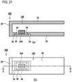
- Figure 21(a) is a schematic cross-sectional view of the boost antenna 100 according to a sixth aspect along a C-C' plane in Figure 21(b) and Figure 21(b) is a schematic plan view of the boost antenna 100 of the sixth aspect viewed from the ground unit 30 side.
- the boost antenna 100 according to the sixth aspect described in Figure 21(a) and Figure 21(b) is similar to the boost antenna 100 described in Figure 3 and Figure 4 in that the radiation unit 10, the short circuit unit 20 and the ground unit 30 are integrally formed.
- the boost antenna 100 of the sixth aspect is further provided with a mounting unit 36 for mounting the RFID tag 200, made of a conductive material and formed separately.
- a through hole 34 which is larger in width and length than the RFID tag 200 in a plan view, is formed in the mounting region of the RFID tag 200 of the ground unit 30, and a notch 35 is formed on an outer surface around the through hole 34 of the ground unit 30.
- the boost antenna 100 of the sixth aspect by bonding the mounting unit 36 on which the RFID tag 200 is mounted to the notch 35 of the ground unit 30, the RFID tag 200 is mounted on the boost antenna 100.
- the length of the notch 35 in the longitudinal direction of the ground unit 30 is made longer than the length of the mounting unit 36, a certain gap is provided between an end of the mounting unit 36 and an end of the notch 35 so that when the mounting unit 36 and the notch 35 are bonded together, the mounting unit 36 is allowed to slide in the longitudinal direction of the ground unit 30.
- the mounting unit 36 on which the RFID tag 200 is mounted can be attached from an outer surface of the ground unit 30, and workability in mounting the RFID tag 200 improves.
- the length of the notch 35 in the longitudinal direction of the ground unit 30 and the length of the mounting unit 36 may be set on the same level.
- Figure 22(a) is a schematic cross-sectional view of a boost antenna 100 according to a seventh aspect along a D-D' plane in Figure 22(b) and Figure 22(b) is a schematic plan view of the boost antenna 100 of the seventh aspect viewed from the ground unit 30 side and Figure 22(c) is a schematic plan view when a plurality of pockets 51 in Figure 22(b) are formed so as to overlap each other.
- the boost antenna 100 according to the seventh aspect described in Figure 22(a) and Figure 22(b) is similar to the boost antenna 100 described in Figure 3 and Figure 4 in that the radiation unit 10, the short circuit unit 20 and the ground unit 30 are integrally formed.
- an insulating support member 50 having a high relative permittivity is inserted between the radiation unit 10 and the ground unit 30 of the boost antenna 100 to thereby shorten the effective wavelength of a radio wave and reduce the shape of the boost antenna 100 with respect to the same resonance frequency.
- the insulating support member 50 and the short circuit unit 20 are not in contact with each other, whereas the boost antenna 100 of the seventh aspect is different in that one end portion of the insulating support member 50 is in contact with the short circuit unit 20.
- the RFID tag 200 is not in contact with the insulating support member 50, whereas the boost antenna 100 of the seventh aspect is different in that the insulating support member 50 includes the pockets 51 for positioning the RFID tag 200, and the RFID tag 200 is stored in the pocket 51.
- the RFID tag 200 can be disposed at a predetermined position by storing the RFID tag 200 in the pocket 51 of the insulating support member 50, then inserting the insulating support member 50 in a space of the boost antenna 100 and bring the insulating support member 50 into contact with the short circuit unit 20. This improves workability in mounting the RFID tag 200 on the boost antenna 100.
- the number of pockets 51 of the insulating support member 50 may be one or plural. As described in Figure 22(b) , when a plurality of pockets 51 with different distances from the short circuit unit 20 are provided, by selecting a pocket 51 to store the RFID tag 200, it is possible to easily adjust the distance of the RFID tag 200 from the short circuit unit 20 and tune the resonance frequency of the RFID tag 300 with a boost antenna to a target.
- a plurality of RFID tags 200 can be stored in the plurality of pockets 51.
- resonance frequencies formed by each RFID tag 200 and the boost antenna 100 differ, and so the RFID tag 300 with a boost antenna can be provided with a plurality of different resonance frequencies and it is possible to support wider band communication frequencies.
- the plurality of pockets 51 may be formed so as to overlap each other as described in Figure 22(c) .
- Figure 23(a) is a schematic cross-sectional view of a boost antenna 100 according to an eighth aspect along an_E-E' plane in Figure 23(b) and Figure 23(b) is a schematic plan view of the boost antenna 100 of the eighth aspect viewed from the ground unit 30 side.
- the boost antenna 100 according to the eighth aspect described in Figure 23(a) and Figure 23(b) is similar to the boost antenna 100 in Figure 22 in that the radiation unit 10, the short circuit unit 20 and the ground unit 30 are integrally formed, the insulating support member 50 is inserted in a space formed between the radiation unit 10 and the ground unit 30, one end portion of the insulating support member 50 is in contact with the short circuit unit 20, and a plurality of pockets 51 for positioning the RFID tag 200 are provided.
- the boost antenna 100 of the seventh aspect is different in that the insulating support member 50 is formed only around both ends in the longitudinal direction of the ground unit 30, around both ends in the width direction, and around the pocket 51. That is, the insulating support member 50 is a frame body, includes a support unit 52 that connects the frame body in the width direction of the ground unit 30 and the pockets 51 are provided on the ground unit 30 side of the support unit 52.
- the wavelength of a radio wave is proportional to the reciprocal of the square root of a relative permittivity. Therefore, filling the space between the radiation unit 10 and the ground unit 30 with the insulating support member 50 having a large relative permittivity shortens the wavelength of the radio wave, and as a result, the boost antenna 100 can be made smaller.
- dielectric loss is caused by filling the space between the radiation unit 10 and the ground unit 30 with the insulating support member 50.
- the insulating support member 50 is filled only at the opening end side, the short circuit unit 20 side, the portion facing both ends in the width direction of the ground unit 30, and around the pockets 51 in which the RFID tag 200 is stored.
- Filling the insulating support member 50 at the opening end side is effective as the position of dielectric for miniaturization. Filling the insulating support member 50 at the short circuit unit 20 side is important for positioning the pockets 51 and the RFID tag 200. This is intended to miniaturize the boost antenna 100, minimize induction loss by the insulating support member 50, and protect the tag with the insulating support member 50.
- the entire space between the radiation unit 10 and the ground unit 30 is filled with the insulating support member 50, whereas a region without any insulating support member 50 may be provided in part of the space between the radiation unit 10 and the ground unit 30 as in the case of the insulating support member 50 in Figure 23 .
- a plurality of RFID tags 200 can be stored in the plurality of pockets 51.
- the reader/writer of the RFID tag 300 with a boost antenna specifies which RFID tag 200 memory to read from or which RFID tag 200 memory to write to, and thereby allows the RFID tag 300 with a boost antenna to function as the RFID tag 300 with a boost antenna having a large memory capacity that sums up memories of the plurality of RFID tags 200.
- a conductor 350 provided with an RFID tag with a boost antenna according to a second embodiment includes the RFID tag 300 with a boost antenna according to the first embodiment fixed to the conductor 310.
- the conductor 350 provided with the RFID tag with a boost antenna according to the second embodiment is described in Figure 1 and Figure 2 .
- Examples of the conductor 310 include various metal objects requiring use histories when used, devices like jigs or tools used for various industrial processes such as machining, metal working, resin processing. Such devices include consumable ones such as cutting or polishing devices as well. Examples of the conductor 310 include not only industrial devices but also objects with metal surfaces such as daily necessities for household use, agricultural products, various prepaid cards for transportation facilities, or medical equipment.
- the ground unit 30 of the boost antenna 100 is preferably grounded to the conductor 310.
- the conductor 310 functions as an extension of the ground unit 30 of the RFID tag 300 with a boost antenna, which improves antenna gain and improves the communication distance of the RFID tag 300 with a boost antenna.
- the ground unit 30 may be electrically grounded via a capacitance of an adhesive layer or the like.
- the short circuit unit 20 of the boost antenna 100 is preferably disposed in the vicinity of one side of the conductor 310 as described in Figure 2 . Furthermore, it is preferable to dispose the radiation unit 10 of the boost antenna 100 in the vicinity of another side adjacent to the one side of the conductor 310 so that the Y direction of the radiation unit 10 is parallel to the another side. Such placement allows the RFID tag 300 with a boost antenna to improve the communication distance thereof.
- An RFID system 400 with a boost antenna combines: the RFID tag 300 with a boost antenna of the first embodiment and an RFID reader/writer 410 including an antenna 420 that transmits/receives a radio wave.
- the RFID system 400 communicates with each other and makes information to be recorded in the RFID tag 200 rewritable at any time.
- a configuration of the RFID system 400 with a boost antenna of the third embodiment is shown in Figure 24 .
- the RFID tag 300 with a boost antenna is identical to the RFID tag 300 with a boost antenna described in Figure 1 and Figure 2 .
- the RFID reader/writer 410 includes an antenna 420 that transmits/receives a radio wave to/from the RFID tag 300 with a boost antenna.
- the RFID reader/writer 410 is, for example, formed by providing the rectangular antenna 420 on a substrate 430 made of an electric insulating material.
- the substrate 430 may be a housing (not shown) that stores the antenna 420.
- the RFID system 400 with a boost antenna of the third embodiment can improve the communication distance significantly.
- the boost antenna 100 corresponds to a "boost antenna”
- the RFID tag 200 corresponds to a “RFID tag”
- the RFID tag 300 with a boost antenna corresponds to a "RFID tag with a boost antenna”
- the radiation unit 10 corresponds to a “radiation unit”
- the short circuit unit 20 corresponds to a “short circuit unit”
- the ground unit 30 corresponds to a "ground unit”
- the ground plate 220 corresponds to a "ground plate”
- the radiation plate 210 corresponds to a “radiation plate”
- the conductor 310 corresponds to a "conductor”
- the protrusion 70 corresponds to a "protrusion”
- the connection part 21 corresponds to a "connection part”
- the opening region 11 corresponds to an “opening region”
- the opening hole 12 corresponds to an “opening hole”
- the resin 55 corresponds to "resin”
- the first groove 31 corresponds to a "first groove”
- the second groove 32 corresponds
Abstract
Description
- The present invention relates to an RFID tag with a boost antenna, a conductor provided with an RFID tag with a boost antenna, and an RFID system including an RFID tag with a boost antenna.
- In recent years, small RFID tags are used in various fields of physical distribution or the like. However, since the small RFID tags are inferior in communication characteristics, there is a demand for improvement in communication distances in the small RFID tags.
- Patent Literature 1 (
Japanese Patent Laid-Open No.1999-68449 - Patent Literature 2 (
Japanese Patent No.4892608 - Patent Literature 3 (
U.S. Patent No.8851388 ) discloses an RFID tag including: a grounding casing made from a conductive material; a coupling casing made from the conductive material and disposed opposite to the grounding casing including a coupling part and a covering part; and an RFID module including an RFID chip and a coupling member electrically coupled with the RFID chip, in which detection sensitivity of the RFID tag is increased and the length of one end short circuit state of said coupling casing is a quarter wavelength. - Patent Literature 4 (
Japanese Patent No.6360264 -
- Patent Literature 1:
Japanese Patent Laid-Open No. 1999-68449 - Patent Literature 2:
Japanese Patent No.4892608 - Patent Literature 3:
U.S. Patent No.8851388 - Patent Literature 4:
Japanese Patent No.6360264 - An RFID system uses an RFID tag provided with an antenna and an IC chip. An RFID tag receives a radio wave (carrier) transmitted from an antenna of a reading device by an antenna of the RFID tag. The RFID tag sends back identification data or the like of a transported object recorded in the IC chip to an RFID reader/writer on a reflected wave. This allows the RFID tag to communicate with the RFID reader/writer without touching the RFID reader/writer to the RFID tag. Note that some RFID readers/writers have a writing function to write information to the RFID tag.
- Recently, there are cases where in a high heat environment such as an automobile manufacturing line, an RFID tag is attached to a vehicle body and the RFID tag is used for management in a manufacturing process. For such an application, a small RFID tag that can be disposed on a metal and has heat resistance is under development.
- However, with the small RFID tag, the shape of the antenna is limited, antenna gain decreases, making it impossible to secure a sufficient communication distance, and so it is necessary to improve the communication distance of the heat-resistant small RFID tag.
- A standard of transmission/reception frequency of the RFID varies from country to country, and so there is a demand for realization of a dual-band compatible RFID tag which can transmit and receive at two different frequencies and a wideband RFID tag which can transmit and receive in a wide frequency band.
- According to the disclosure described in
Patent Literature 1, the antenna body is an inverted F antenna and is mounted on metal. By selecting a horizontal distance and a vertical distance between the radiation conductor plate and the linear non-feeding antenna element of the antenna body, improvement on the order of 6 dB to 7 dB has been achieved. - However, in the case of the disclosure described in
Patent Literature 1, a separate insulating support instrument or the like is necessary to appropriately fix the horizontal distance and the vertical distance between the radiation conductor plate and the linear non-feeding antenna element of the antenna body, which results in that the structure of the boost antenna becomes complicated. - The EM tag described in
Patent Literature 2 is a UHF tag provided with a dipole antenna as described, for example, inFigure 4 and the cavity described inPatent Literature 2 is intended to decouple the UHF tag provided with the dipole antenna from the metal surface, sensitivity of the dipole antenna would normally drastically deteriorate when disposed on the metal surface, and to prevent the sensitivity of the UHF tag from deteriorating. However, the dipole antenna described inFigure 4 is large, having a length of 95 mm, and moreover, the disclosure described inPatent Literature 2 is not applicable to a planar inverted-F antenna or the like that is becoming smaller. - The RFID tag described in
Patent Literature 3 is an RFID tag with an RFID module disposed on a grounding casing of a housing constructed of the grounding casing and the coupling casing. The housing of the RFID tag described inPatent Literature 3 is provided with a shape of a planar inverted-F antenna and the length of the coupling casing is 1/4λ, and so a resonance frequency of the housing provided with the shape of the planar inverted-F antenna corresponds to a resonance frequency of the RFID tag, and the RFID module itself has no resonance characteristic. However, an RFID module provided with an antenna normally has resonance characteristics, and the disclosure described inPatent Literature 3 is not applicable to the RFID module provided with the antenna. - The RFID tag described in
Patent Literature 4 implements a small RFID tag with a built-in inverted F antenna by using a ceramic multilayer substrate, disposing the RFID chip inside the multilayer substrate and providing a capacity conductor that applies a capacitance to the antenna conductor, but the communication distance as the RFID may be insufficient depending on the application. - It is a principal object of the present invention to provide an RFID tag with a boost antenna, a conductor provided with the RFID tag with a boost antenna, and an RFID system including the RFID tag with a boost antenna, that can improve a communication distance by combining a boost antenna with a small RFID tag.
- It is another object of the present invention to provide an RFID tag with a boost antenna that can adjust two resonance frequencies provided in the RFID tag with a boost antenna to enable transmission/reception in a wideband or in two frequency bands by adjusting a resonance frequency of the RFID tag and the boost antenna, and a coupling coefficient between the RFID tag and the boost antenna.
- An RFID tag with a boost antenna according to one aspect is an RFID tag with a boost antenna including a boost antenna and an RFID tag, in which the boost antenna includes: a conductive radiation unit; a conductive ground unit facing the radiation unit; and a short circuit unit that connects one end of the radiation unit and one end of the ground unit, and electrically conducts the radiation unit and the ground unit to each other, the RFID tag is disposed between the radiation unit and the ground unit of the boost antenna and at a position closer to the short circuit unit than to a center position in a longitudinal direction of the radiation unit, and the boost antenna and the RFID tag each have resonance characteristics.
- In this case, when the resonator provided in the RFID tag and the resonator provided in the boost antenna are coupled, energy propagates from the RFID tag to the boost antenna efficiently. Furthermore, since a radio wave radiates from the boost antenna providing the inverted-L antenna structure and having high antenna gain, it is possible to improve a communication distance of the RFID tag with a boost antenna compared with the RFID tag as a single unit.
- Since the boost antenna and the RFID tag have respective resonance frequencies as single units, and as a result, the RFID tag with a boost antenna also has two resonance frequencies, it is possible to implement a dual-band compatible RFID tag, and a wideband RFID tag by adjusting the two resonance frequencies.
- Since the RFID tag is fixed to an object such as a conductor via the boost antenna, heat transfer is weak compared to a case where the RFID tag is directly fixed to the object, and as a result, it is possible to improve heat resistance of the RFID tag.
- An RFID tag with a boost antenna according to a second invention is the RFID tag with a boost antenna according to the one aspect, in which the short circuit unit, the radiation unit, and the ground unit may have a same width, and the short circuit unit may have a rectangular parallelepiped shape.
- In this case, since the shape of the boost antenna is simple, manufacturing is easy.
- An RFID tag with a boost antenna according to a third invention is the RFID tag with a boost antenna according to the one aspect or the second invention, in which the radiation unit, the short circuit unit, and the ground unit may be integrated.
- In this case, it is possible to easily manufacture the boost antenna using a method such as folding one rectangular metal or applying extrusion processing from an aluminum material.
- An RFID tag with a boost antenna according to a fourth invention is the RFID tag with a boost antenna according to the one aspect, in which the short circuit unit may be constructed of one or a plurality of posts.
- In this case, by adjusting the positions of the posts and/or the number of posts of the short circuit unit, it is possible to adjust the resonance frequency of the boost antenna and the coupling coefficient between the boost antenna and the RFID tag when the RFID tag is disposed on the boost antenna, with respect to the boost antenna having the same shape of the radiation unit. Note that the "posts" used in the present invention mean struts that connect the radiation unit and the ground unit.
- An RFID tag with a boost antenna according to a fifth invention is the RFID tag with a boost antenna according to from the one aspect to the fourth invention, in which the ground unit may include a protrusion for positioning the RFID tag.
- In this case, it is possible to reduce variations in the position of the RFID tag disposed on the ground unit of the boost antenna, and suppress variations in characteristics such as the resonance frequency of the RFID tag with the boost antenna.
- An RFID tag with a boost antenna according to a sixth invention is the RFID tag with a boost antenna according to from the one aspect to the fourth invention, in which the ground unit may include a fixing tool to fix the RFID tag.
- In this case, since the RFID tag is fixed to the boost antenna with the fixing tool, the RFID tag need not be fixed using an adhesive, and heat resistance of the RFID tag with a boost antenna can be improved.
- An RFID tag with a boost antenna according to a seventh invention is the RFID tag with a boost antenna according to from the one aspect to the second invention, in which the radiation unit and the short circuit unit are integrated, the ground unit is separate from the radiation unit and the short circuit unit, and a connection part provided in the short circuit unit may be connected to the ground unit on which the RFID tag is mounted.
- In this case, the RFID tag is mounted on the ground unit first, and the integrated radiation unit and short circuit unit are then connected to the ground unit using the connection part provided in the short circuit unit, and it is thereby possible to improve workability of mounting the RFID tag on the boost antenna.
- An RFID tag with a boost antenna according to an eighth invention is the RFID tag with a boost antenna according to the seventh invention, in which the connection part and the ground unit may be slidably connected in the longitudinal direction of the ground unit.
- In this case, by adjusting the distance between the short circuit unit and the RFID tag, it is possible to adjust the resonance frequency of the RFID tag with a boost antenna, and so even when, for example, the resonance frequency of the RFID tag varies from lot to lot, it is possible to tune the resonance frequency of the RFID tag with a boost antenna to a target frequency.
- An RFID tag with a boost antenna according to a ninth invention is the RFID tag with a boost antenna according to the third invention, in which the ground unit may include a mounting region of the RFID tag on the inner surface on the side facing the radiation unit, and the radiation unit may include an opening region larger in width and length in a plan view than the mounting region at a position facing the mounting region.
- In this case, forming an opening region larger than the mounting region in the radiation unit makes it easier to dispose the RFID tag from the opening region in the ground unit mounting region when mounting the RFID tag on the boost antenna.
- An RFID tag with a boost antenna according to a tenth invention is the RFID tag with a boost antenna according to the ninth invention, in which the mounting region may be a convex top surface.
- In this case, steps at ends of the mounting region make it possible to easily recognize the RFID tag mounting position.
- An RFID tag with a boost antenna according to an eleventh invention is the RFID tag with a boost antenna according to the ninth or tenth invention, in which the ground unit may include a first groove around the mounting region.
- In this case, the first groove makes it possible to easily recognize the RFID tag mounting position.
- Applying an adhesive to the mounting region and the first groove therearound can improve bonding strength between the RFID tag and the ground unit.
- An RFID tag with a boost antenna according to a twelfth invention is the RFID tag with a boost antenna according to the third or ninth invention, in which a space formed between the radiation unit and the ground unit on which the RFID tag is mounted may be filled with resin.
- In this case, adhesive strength of the resin allows the RFID tag to be fixed to the boost antenna more strongly. The resin surrounding the RFID tag can protect the RFID tag. When the opening region is formed in the radiation unit, resin penetrates into the opening region, which makes it harder for the resin and the RFID tag to come off the boost antenna.
- An RFID tag with a boost antenna according to a thirteenth invention is the RFID tag with a boost antenna according to the twelfth invention, further including an opening hole in at least one of the radiation unit and the ground unit, in which resin may penetrate into the opening hole.
- In this case, the resin penetrates into the opening hole, which makes it much harder for the resin and the RFID tag to come off the boost antenna.
- An RFID tag with a boost antenna according to a fourteenth invention is the RFID tag with a boost antenna according to the third invention, in which the ground unit may include a second groove on the inner surface on a side facing the radiation unit, and the second groove may extend from a side surface in a width direction of the ground unit to the mounting region of the RFID tag.
- In this case, by sliding the RFID tag along the second groove makes it easy to dispose the RFID tag in the mounting region of the ground unit.
- An RFID tag with a boost antenna according to a fifteenth invention is the RFID tag with a boost antenna according to the fourteenth invention, further including a third groove that extends from the mounting region in the longitudinal direction of the ground unit.
- In this case, by sliding the RFID tag disposed in the mounting region along the third groove in the longitudinal direction of the ground unit, it is possible to adjust the distance between the RFID tag and the short circuit unit and tune the resonance frequency of the RFID tag with a boost antenna to a target frequency.
- An RFID tag with a boost antenna according to a sixteenth invention is the RFID tag with a boost antenna according to the third invention, further including a separate mounting unit made of a conductive material for mounting the RFID tag, in which the ground unit may further include a through hole which is larger in width and length in a plan view than the RFID tag and a notch located on an outer surface around the through hole, and the mounting unit may engage with the notch.
- In this case, by attaching the mounting unit on which the RFID tag is mounted from the outer surface of the ground unit, it is possible to improve workability of mounting the RFID tag on the boost antenna.
- An RFID tag with a boost antenna according to a seventeenth invention is the RFID tag with a boost antenna according to the sixteenth invention, in which the length of the notch in the longitudinal direction of the ground unit may be longer than the length of the mounting unit.
- In this case, in the engagement between the mounting unit and the notch, by sliding the mounting unit in the longitudinal direction of the ground unit, it is possible to adjust the distance between the RFID tag and the short circuit unit and tune the resonance frequency of the RFID tag with a boost antenna to a target.
- An RFID tag with a boost antenna according to an eighteenth invention is the RFID tag with a boost antenna according to from the first aspect to the seventeenth invention, in which the RFID tag with a boost antenna may be configured to adjust the resonance frequency of the boost antenna, the resonance frequency of the RFID tag, and the coupling coefficient between the boost antenna and the RFID tag to enable transmission/reception at two different frequency bands.
- In the RFID tag with a boost antenna, the RFID tag as a single unit and the boost antenna as a single unit are each provided with a resonance frequency. In this case, the RFID tag with a boost antenna is provided with two resonance frequencies different from the resonance frequency of the RFID tag as a single unit and the resonance frequency of the boost antenna as a single unit. The resonance frequency of the RFID tag with a boost antenna changes depending on the resonance frequency of the boost antenna and the resonance frequency of the RFID tag, and a coupling coefficient between the boost antenna and the RFID tag.
- Therefore, the RFID tag with a boost antenna can be constructed by adjusting the resonance frequency of the boost antenna and the resonance frequency of the RFID tag and the coupling coefficient between the boost antenna and the RFID tag, and tuning the two resonance frequencies of the RFID tag with a boost antenna to the two necessary transmission/reception frequencies.
- Note that the coupling coefficient between the boost antenna and the RFID tag can be adjusted by changing, for example, the distance between the radiation unit and the ground unit of the boost antenna, the shape of the short circuit unit of the boost antenna, the position and/or the direction of the RFID tag disposed in the ground unit of the boost antenna.
- An RFID tag with a boost antenna according to a nineteenth invention is the RFID tag with a boost antenna according to from the one aspect to the seventeenth invention, in which the RFID tag with a boost antenna may be configured to adjust the resonance frequency of the boost antenna, the resonance frequency of the RFID tag, and the coupling coefficient between the boost antenna and the RFID tag, and widen the transmission/reception frequency band.
- For an antenna provided with two resonance frequencies, a wideband antenna can be configured by bringing the two resonance frequencies closer together.
- On the other hand, in the invention according to the one aspect, the boost antenna and the RFID tag are each provided with resonance characteristics, and the resonator provided in the RFID tag and the resonator provided in the boost antenna are coupled together. In this case, two resonance frequencies can be brought closer together by reducing the coupling coefficient.
- Therefore, a wideband antenna can be constructed by adjusting the resonance frequency of the boost antenna and the resonance frequency of the RFID tag, and the coupling coefficient between the boost antenna and the RFID tag.
- An RFID tag with a boost antenna according to a twentieth invention is the RFID tag with a boost antenna according to from the one aspect to the nineteenth invention, in which an insulating support member may be inserted in a space formed between the radiation unit and the ground unit.
- The insulating support member has an effect of stabilizing the distance between the radiation unit and the ground unit.
- Using a material of a high relative permittivity as the insulating support member, it is possible to shorten the wavelength of an electromagnetic wave passing through the insulating support member. By shortening the wavelength of the electromagnetic wave, it is possible to reduce the resonance frequency for the boost antenna of the same shape or reduce the shape for the boost antenna of the same resonance frequency.
- Furthermore, the above effect also varies depending on the position at which the insulating support member is inserted, and inserting the insulating support member on the other end (opening end) side of the radiation plate and the ground plate produces a greater effect.
- Therefore, by fixing the shapes of the radiation unit and the ground unit of the boost antenna and adjusting the position of the insulating support member, it is also possible to adjust the resonance frequency.
- An RFID tag with a boost antenna according to a twenty-first invention is the RFID tag with a boost antenna according to the twentieth invention, in which one end of the insulating support member may contact the short circuit unit and the insulating support member may include at least one pocket for positioning the RFID tag.
- In this case, by storing the RFID tag in the pocket of the insulating support member and then inserting the insulating support member into the space of the boost antenna to contact the short circuit unit, it is possible to accurately dispose the RFID tag in the predetermined mounting region. This improves workability of mounting the RFID tag on the boost antenna.
- Note that the radiation unit and the ground unit of the boost antenna are preferrably parallel to each other so as to smoothly insert the insulating support member into the space of the boost antenna and so that the insulating support member and the radiation unit, the short circuit unit, and the ground unit of the boost antenna are brought into close contact with each other without gaps.
- An RFID tag with a boost antenna according to a twenty-second invention is the RFID tag with a boost antenna according to the twenty-first invention, in which the insulating support member may be a frame body and may include a support portion to connect the frame body in the width direction of the ground unit, and the pocket may be provided on the ground unit side of the support portion.
- In this case, it is possible to reduce the size of the boost antenna, minimize dielectric loss due to the insulating support member, and protect the tag by the insulating support member, by filling the insulating support member only at the opening end side, the short circuit unit side, the portion facing both ends in the width direction of the ground unit, and around the pocket in which the RFID tag is stored. Filling the insulating support member at the opening end side is effective as the dielectric position for miniaturization. Filling the insulating support member at the short circuit unit side is important for positioning the pocket and the RFID tag.
- An RFID tag with a boost antenna according to a twenty-third invention is the RFID tag with a boost antenna according to the twenty-first or twenty-second invention, in which the insulating support member includes a plurality of pockets having different distances from the short circuit unit and the RFID tag may be stored in one of the plurality of pockets.
- In this case, by selecting a pocket in which the RFID tag is stored, it is possible to easily and accurately adjust the distance from the short circuit unit of the RFID tag and tune the resonance frequency of the RFID tag with a boost antenna to a target.
- An RFID tag with a boost antenna according to a twenty-fourth invention is the RFID tag with a boost antenna according to the twenty-first or twenty-second invention, in which the insulating support member includes a plurality of pockets having different distances from the short circuit unit and a plurality of RFID tags may be stored in the plurality of pockets.
- Note that the number of RFID tags stored is equal to or smaller than the number of pockets. For example, when there are three pockets having different distances from the short circuit unit, the RFID tag may be stored in two out of three pockets.
- When a plurality of RFID tags are stored in a plurality of pockets having different distances from the short circuit unit, a resonance frequency formed of each RFID tag and each boost antenna differs from each other, and so the RFID tag with a boost antenna can be provided with a plurality of different resonance frequencies and can respond to wider communication frequency bands.
- An RFID tag with a boost antenna according to a twenty-fifth invention is the RFID tag with a boost antenna according to the twenty-first or twenty-second invention, further including a plurality of pockets, in which a plurality of RFID tags provided with memories may be stored in the plurality of pockets.
- Note that the number of RFID tags stored is equal to or smaller than the number of pockets. For example, when there are three pockets, the RFID tag may be stored in two out of three pockets.
- In this case, by specifying which RFID tag memory the reader/writer of the RFID tag with a boost antenna should read from, or which RFID tag memory the reader/writer should write to, it is possible to allow the RFID tag with a boost antenna to function as an RFID tag with a large memory capacity summing memories of the plurality of RFID tags.
- An RFID tag with a boost antenna according to a twenty-sixth invention is the RFID tag with a boost antenna according to from the one aspect to the twenty-fifth invention, in which the RFID tag is an inverted-F antenna type RFID tag, the RFID tag including: an insulating substrate; a radiation plate provided on the top surface of the insulating substrate; a ground plate provided on an undersurface of the insulating substrate; a short circuit conductor connected to the radiation plate and the ground plate; and an IC chip connected to the radiation plate and the ground plate, and the RFID tag may be disposed so that the short circuit conductor is located on a side farthest from the short circuit unit or on a side closest to the short circuit unit.
- By using the inverted-F antenna type RFID tag as the RFID tag and disposing the RFID tag on the ground plate of the boost antenna, it is possible to increase directivity in the zenith direction of the RFID tag, and efficiently send an electromagnetic wave radiated from the RFID tag to the radiation unit of the boost antenna.
- In the inverted-F antenna type RFID tag, the short circuit conductor is disposed in the vicinity of one side surface of the insulating substrate and side surface facing this one side surface becomes an opening of the RFID tag. By disposing the RFID tag in the above direction, it is possible to match the direction of the electric field and the magnetic field of the RFID tag with the direction of the electric field and the magnetic field of the boost antenna when the boost antenna resonates, and send energy from the RFID tag via the boost antenna more efficiently.
- An RFID tag with a boost antenna according to a twenty-seventh invention is the RFID tag with a boost antenna according to the twenty-sixth invention, in which the RFID tag may be disposed so that the short circuit conductor is located on the side farthest from the short circuit unit.
- In this case, the opening of the RFID tag is directed toward the short circuit unit of the boost antenna. In the boost antenna having an inverted-L structure, the short circuit unit corresponds to a node with the smallest amplitude of the standing wave at resonance. Therefore, the electromagnetic wave can be sent from the RFID tag to the radiation unit more efficiently by disposing the short circuit conductor of the RFID tag on the side farthest from the short circuit unit and disposing the opening of the RFID tag toward the short circuit unit.
- A conductor provided with the RFID tag with a boost antenna according to a twenty-eighth invention may be configured to fix the RFID tag with a boost antenna according to from the one aspect to the twenty-seventh invention to a surface of the conductor and electrically connect the ground unit of the boost antenna and the surface of the conductor directly or via a capacitance.
- In this case, since the conductor becomes an extension of the ground unit of the boost antenna and the RFID tag with a boost antenna substantially operates as the RFID tag with a boost antenna with expanded area of the ground unit of the boost antenna, the communication distance of the RFID tag with a boost antenna can be improved.
- When the dipole antenna type RFID tag is fixed to the conductor surface, the communication distance of the RFID tag becomes considerably shorter under the influence of the conductor. However, when the RFID tag with a boost antenna of the present invention is fixed to the surface of the conductor, the communication distance can be improved.
- An RFID system including the RFID tag with a boost antenna according to a twenty-ninth invention includes the RFID tag with a boost antenna according to from the one aspect to the twenty-seventh invention and an RFID reader/writer provided with an antenna that transmits/receives a radio wave to/from the RFID tag with a boost antenna.
- In this case, the RFID tag with a boost antenna is mounted on and used for various objects and various information on the objects is written in the RFID tag. The information is rewritable at any time according to information transmitted/received between the RFID reader/writer and the RFID tag with a boost antenna in the RFID system including the RFID tag with a boost antenna.
- Since the RFID system can vastly improve the communication distance of the RFID tag with a boost antenna, communication can be carried out even when there is a large distance between the RFID tag with a boost antenna and the RFID reader/writer.
-
- [
Figure 1] Figure 1 is a schematic side view of an RFID tag with a boost antenna fixed to a conductor. - [
Figure 2] Figure 2 is a schematic top view of the RFID tag with a boost antenna fixed to the conductor. - [
Figure 3] Figure 3 is a schematic side view of the boost antenna. - [
Figure 4] Figure 4 is a schematic top view of the boost antenna. - [
Figure 5] Figure 5 is a schematic top view illustrating a shape of a short circuit unit of the boost antenna. - [
Figure 6] Figure 6 is a schematic side view of the boost antenna provided with a metal fitting. - [
Figure 7] Figure 7 is a diagram illustrating the shape of the boost antenna used for a simulation of a resonance frequency. - [
Figure 8] Figure 8 is a diagram illustrating simulation results of the resonance frequency of the boost antenna. - [
Figure 9] Figure 9 is a diagram illustrating a structure of the RFID tag. - [
Figure 10] Figure 10 is a diagram illustrating directivity of the RFID tag. - [
Figure 11] Figure 11 is a diagram illustrating measurement results of frequency characteristics of a communication distance of the RFID tag with a boost antenna. - [
Figure 12] Figure 12 is a diagram illustrating simulation results of frequency characteristics of antenna gain of a dual-band compatible RFID tag with a boost antenna. - [
Figure 13] Figure 13 is a diagram illustrating measurement results of frequency characteristics of a communication distance of the dual-band compatible RFID tag with a boost antenna. - [
Figure 14 ]Figure 14(a) is a schematic view illustrating a position of the RFID tag of the RFID tag with a boost antenna andFigure 14(b) is a diagram illustrating simulation results of a correlation between a distance D between the RFID tag and the short circuit unit, and the resonance frequency of the RFID tag with a boost antenna. - [
Figure 15] Figure 15 is a diagram illustrating simulation results of a relationship between a position of the RFID tag and antenna gain of the RFID tag with a boost antenna. - [
Figure 16] Figure 16 is a diagram illustrating simulation results of the relationship between the position of the support member and the antenna gain in case an insulating support member is inserted into the RFID tag with a boost antenna. - [
Figure 17] Figure 17(a) is a schematic side view of a boost antenna according to a second aspect, andFigure 17(b) is a schematic plan view of the boost antenna of the second aspect viewed from the radiation unit side. - [
Figure 18] Figure 18(a) is a schematic cross-sectional view along an A-A' plane inFigure 18(b) of a boost antenna according to a third aspect, andFigure 18(b) is a schematic plan view of the boost antenna of the third aspect viewed from the radiation unit side. - [
Figure 19] Figure 19(a) is a schematic plan view of a boost antenna according to a fourth aspect viewed from the radiation unit side, andFigure 19(b) is a schematic cross-sectional view along a B-B' plane inFigure 19(a) of the boost antenna of the fourth aspect. - [
Figure 20] Figure 20(a) is a schematic side view of a boost antenna according to a fifth aspect andFigure 20(b) is a schematic cross-sectional view along a C-C' plane inFigure 20(a) of the boost antenna of the fifth aspect. - [
Figure 21] Figure 21(a) is a schematic cross-sectional view along a D-D' plane inFigure 21(b) of a boost antenna according to a sixth aspect, andFigure 21(b) is a schematic plan view of the boost antenna of the sixth aspect viewed from the ground unit side. - [
Figure 22] Figure 22(a) is a schematic cross-sectional view along an E-E' plane inFigure 22(b) of a boost antenna according to a seventh aspect,Figure 22(b) is a schematic plan view of the boost antenna of the seventh aspect viewed from the ground unit side, andFigure 22(c) is a schematic plan view when a plurality of pockets inFigure 22(b) are formed so as to overlap each other. - [
Figure 23] Figure 23(a) is a schematic cross-sectional view along an F-F' plane inFigure 23(b) of a boost antenna according to an eighth aspect, andFigure 23(b) is a schematic plan view of the boost antenna of the eighth aspect viewed from the ground unit side. - [
Figure 24] Figure 24 is a diagram illustrating a configuration of an RFID system with a boost antenna. - Hereinafter, embodiments of the present invention will be described with reference to the accompanying drawings. In the following description, identical components are assigned identical reference numerals. When reference numerals are identical, names and functions thereof are also identical. Therefore, detailed description thereof will not be repeated.
-
Figure 1 is a schematic side view of anRFID tag 300 with a boost antenna according to a first embodiment fixed to aconductor 310, andFigure 2 is a schematic top view of theRFID tag 300 with a boost antenna according to the first embodiment fixed to theconductor 310. - The
RFID tag 300 with a boost antenna includes aboost antenna 100 and anRFID tag 200. TheRFID tag 200 is disposed at a position between aradiation unit 10 and aground unit 30 of theboost antenna 100 and closer to ashort circuit unit 20 than to a center position in a longitudinal direction of theradiation unit 10. - In the following description, as described in
Figure 1 and Figure 2 , a direction of a line connecting one end side (short circuit unit 20 side) of theboost antenna 100 and the other end side (opening end side) is assumed to be a Y direction. A direction of a line connecting theground unit 30 and the radiation unit 10 (zenithal direction) is assumed to be a Z direction and a direction orthogonal to the Y direction and the Z direction is assumed to be an X direction. - In
Figure 1 and Figure 2 , theRFID tag 300 with a boost antenna is fixed to theconductor 310. This is because when theRFID tag 300 is fixed to theconductor 310, the communication distance of theRFID tag 300 with a boost antenna further improves. Even when theRFID tag 300 with a boost antenna is fixed to other than theconductor 310, for example, plastic, the communication distance thereof can improve compared to theRFID tag 200 as a single unit. - In
Figure 1 and Figure 2 , although theRFID tag 300 with a boost antenna is directly electrically connected to theconductor 310, theRFID tag 300 with a boost antenna may be fixed to theconductor 310 using an adhesive and connected to theconductor 310 via a capacitance composed of an adhesive layer. -
Figure 3 is a schematic side view of theboost antenna 100 andFigure 4 is a schematic top view of theboost antenna 100. - The
boost antenna 100 is formed of theconductive radiation unit 10, theconductive ground unit 30 facing theradiation unit 10, and theshort circuit unit 20 that connects one end of theradiation unit 10 and one end of theground unit 30 and causes theradiation unit 10 and theground unit 30 to electrically conduct to each other. - As the conductive materials of the
radiation unit 10, theshort circuit unit 20 and theground unit 30 of theboost antenna 100, aluminum, iron or copper is preferably used mainly. In this case, it is possible to form theboost antenna 100 with low resistance and high shape accuracy. - The
boost antenna 100 can be formed by folding one conductor. When the material is aluminum, theboost antenna 100 can also be formed using extrusion molding. - The thicknesses of the conductive materials of the
radiation unit 10, theshort circuit unit 20 and theground unit 30 of theboost antenna 100 are preferably 0.5 mm or more and 3 mm or less. This is because when the thickness of the conductive material is less than 0.5 mm, there is a problem in terms of physical strength of theboost antenna 100, whereas when the thickness exceeds 3 mm, there is a problem in terms of external dimensions and material prices. - In
Figure 3 andFigure 4 , although theshort circuit unit 20 of theboost antenna 100 is formed into a rectangular parallelepiped shape having the same width as the width of theradiation unit 10, theshort circuit unit 20 can also be formed, for example, of one or a plurality of circular or quadrangular column shaped posts. -
Figure 5 is a schematic top view of theboost antenna 100 showing several examples of theshort circuit unit 20. -
Figure 5(a) is the same rectangular parallelepipedshort circuit unit 20 as that inFigure 3 andFigure 4. Figure 5(b) is theshort circuit unit 20 with the one circular column shaped post disposed at the center of theradiation unit 10 in the X direction.Figure 5(c) is theshort circuit unit 20 with two circular column shaped posts disposed in the vicinity of both ends in the X direction of theradiation unit 10.Figure 5(d) is theshort circuit unit 20 with one circular column shaped post disposed in the vicinity of an end in the X direction of theradiation unit 10. - By changing the shape and the position of the
short circuit unit 20, it is possible to change the resonance frequency of theboost antenna 100 and the coupling coefficient between theboost antenna 100 and theRFID tag 200 disposed on theboost antenna 100 even when the shape (width W, length L, height T) of theradiation unit 10 is unchanged. - An insulating
support member 50 may be inserted between theradiation unit 10 and theground unit 30 of theboost antenna 100. In this case, there is less variation in the distance between the opposingradiation unit 10 andground unit 30. By using a material with a high relative permittivity as the insulatingsupport member 50, it is possible to shorten the wavelength of the radio wave and reduce the shape of theradiation unit 10 and theground unit 30 in the insulatingsupport member 50, and increase the substantial opening area of theboost antenna 100. - When the insulating
support member 50 is inserted, by adjusting the position of the insulatingsupport member 50 in the Y direction of theradiation unit 10 of theboost antenna 100, it is possible to adjust the resonance frequency of theboost antenna 100 without changing the shapes of theradiation unit 10 and theground unit 30. - The
ground unit 30 can be provided with aprotrusion 70 for positioning theRFID tag 200 on theground unit 30. Theprotrusion 70 is preferably alinear protrusion 70 orthogonal to a line connecting one end and the other end (an end portion on an opposite side of the one end) of theground unit 30. This is because theRFID tag 200 is easily inserted when theRFID tag 200 is inserted in theboost antenna 100 and theRFID tag 200 has a large variation in characteristics due to a positional shift in the Y direction on theground unit 30. -
Figure 6 shows a schematic side view of theboost antenna 100 provided with ametal fitting 80 to fix theRFID tag 200 to theground unit 30. After theRFID tag 200 is disposed on theground unit 30, the metal fitting 80 can be fixed to theground unit 30 using a screw (not shown) or the like. In this case, theRFID tag 200 can be fixed to theground unit 30 of theboost antenna 100 without having to use any adhesive. Avoiding use of any adhesive with heat resistance problems makes it possible to improve heat resistance of theRFID tag 300 with a boost antenna. - In the
boost antenna 100, theground unit 30 can be provided with a mountinghole 40. In this case, by screwing theboost antenna 100 to theconductor 310, it is possible to reduce variations in relative position between theboost antenna 100 and theconductor 310. - Dependency of the resonance frequency of the
boost antenna 100 on the shape (length L, width W) of theradiation unit 10 was calculated according to an FDTD method using a simple model. The shape of the model used for the calculation is shown inFigure 7 . InFigure 7, Figure 7(a) shows a perspective view, (b) shows a plan view viewed from the X direction, (c) shows a plan view viewed from the Z direction and (d) shows a plan view viewed from the Y direction. Numbers in the drawings represent the respective dimensions and the unit is mm. Note that the above Y direction corresponds to the direction of a line connecting the one end and the other end (end portion on the opposite side of the one end) of theradiation unit 10. - In the model used for the calculation, assuming a case where the
boost antenna 100 is fixed to a metal surface, the area of theground unit 30 is set to 112 mm×56 mm, larger than the area of theradiation unit 10. Although a power supply unit 90 is not included in theboost antenna 100 itself, in the above calculation, the power supply unit 90 is disposed at a position in the vicinity of the center in the X direction of theradiation unit short circuit unit 20. -
Figure 8 shows simulation results of a relationship between a value of 2L+W of theradiation unit 10 and the resonance frequency when the length L and the width W of theradiation unit 10 are changed. InFigure 8 , the resonance frequency of theboost antenna 100 is substantially proportional to 1/(2L+W) and is plotted at a position close to a straight line representing a relationship between 1/(2L+W) and the resonance frequency when a half wavelength of the resonance frequency is equal to 2L+W. - In the case of a standard planar inverted-L antenna, 2(L+W)=(1/2)λ at resonance, whereas in the case of the
boost antenna short circuit unit 20 in theboost antenna 100 inFigure 7 extends over a whole W of theradiation unit 10 and the effective peripheral length of theradiation unit 10 is 2L+W. Note that though not described inFigure 8 , when theshort circuit unit 20 is not formed in the rectangular parallelepiped shape having the same width as the short side of theradiation unit 10 but formed of a post in a columnar shape or the like, the resonance frequency of theboost antenna 100 changes. As shown, for example, inFigure 5(b) , when one column shaped post is disposed at a center position on one end side of theradiation unit 10, the resonance frequency of theboost antenna 100 is lower compared to the case where theshort circuit unit 20 having a rectangular parallelepiped shape of the same width as the width of theradiation unit 10 as shown inFigure 5(a) . -
Figure 9 shows an example of theRFID tag 200.Figure 9(a) shows a schematic top view,Figure 9(b) shows a schematic cross-sectional view andFigure 9(c) shows a schematic bottom view. - The
RFID tag 200 is provided with an insulating substrate 230, aradiation plate 210, aground plate 220, ashort circuit conductor 260, acapacity part conductor 250, a capacitypart penetrating conductor 270 and anIC chip 240. - The
radiation plate 210 is provided on a top surface of the insulating substrate 230, theground plate 220 is provided on an undersurface of the insulating substrate 230, and theradiation plate 210 and theground plate 220 are electrically connected via theshort circuit conductor 260. - The
capacity part conductor 250 is disposed inside the insulating substrate 230 so as to face part of theground plate 220 and connected to theradiation plate 210 via the capacitypart penetrating conductor 270. - The
IC chip 240 is stored in a concave portion provided on the top surface of the insulating substrate 230, electrically connected to theradiation plate 210 and theground plate 220 and functions as a power supply unit. - An antenna of the
RFID tag 200 is an inverted F type antenna. - Note that the reason that the
RFID tag 200 described inFigure 9 is provided with thecapacity part conductor 250 and the capacitypart penetrating conductor 270 is to make smaller the shape of theRFID tag 200 by increasing the capacitance between theradiation plate 210 and theground plate 220. However, when the same resonance frequency is required, the shape of theRFID tag 200 becomes a little larger, but thecapacity part conductor 250 and the capacitypart penetrating conductor 270 may be omissible. -
Figure 10 illustrates an example of simulation results of directivity of theRFID tag 200.Figure 10(b) illustrates a placement direction of theRFID tag 200 in X-Y-Z coordinates andFigure 10(a) illustrates directivity of antenna gain of theRFID tag 200 on an X-Z plane and a Y-Z plane. - In
Figure 10 , the Z direction corresponds to a zenithal direction of theRFID tag 200, that is, an upward direction inFigure 10(b) and the Y direction corresponds to a rightward direction inFigure 10(b) . In the simulation, theRFID tag 200 is disposed on theconductor 310. - The
RFID tag 200 inFigure 10(b) has strong directivity in the zenithal direction, and when theRFID tag 200 is disposed on theground unit 30 of theboost antenna 100, a radio wave is radiated from theRFID tag 200 toward theradiation unit 10, which is suitable. - The
RFID tag 200 shows higher antenna gain in the Y direction than in the X direction and more radio waves are radiated in the Y direction than in the X direction. - The
RFID tag 200 described inFigure 9 is the planar inverted-F antennatype RFID tag 200, but as theRFID tag 200 to be used for the present invention, theRFID tag 200 provided with an antenna having directivity in the zenithal direction such as an inverted-F antenna or a patch antenna when disposed on a metal can be used. - The
RFID tag 300 with a boost antenna is described inFigure 1 and Figure 2 . - In
Figure 1 and Figure 2 , theRFID tag 200 is disposed between theradiation unit 10 and theground unit 30 of theboost antenna 100 and at a position closer to theshort circuit unit 20 than to the center in the Y direction of theradiation unit 10. When theRFID tag 200 is disposed on theground unit 30 of theboost antenna 100, theRFID tag 200 is sandwiched between theprotrusions 70 and bonded thereto, and it is thereby possible to prevent positional shifts in the Y direction of theboost antenna 100. - The
boost antenna 100 can be screwed to theconductor 310 using the mountinghole 40. In this case, it is possible to reduce variations in relative positions of theboost antenna 100 and theconductor 310. - Furthermore, by causing the
boost antenna 100 to electrically conduct to theconductor 310, theconductor 310 is allowed to function as an extension of theground unit 30 of theboost antenna 100. In this case, theboost antenna 100 is substantially equivalent to theboost antenna 100 with theground unit 30 having a large area, which improves the antenna gain. -
Figure 11 illustrates measurement results of communication distances of theRFID tag 200 as a single unit and theRFID tag 300 with a boost antenna measured using Tagformance manufactured by voyantic. - Placing the
RFID tag 200 on theboost antenna 100 so as to function as theRFID tag 300 with a boost antenna significantly improves communication distance from 0.8 m to 2.8 m compared to theRFID tag 200 as a single unit. - With the
RFID tag 200 as a single unit, theboost antenna 100 as a single unit and theRFID tag 300 with a boost antenna disposed on a 200 mm square conductor 310 (copper plate), their respective resonance frequencies were determined by simulation. The shape of theRFID tag 200 was fixed to 6 mm×3 mm×1.7 mm and the shape and structure of theboost antenna 100 were changed. A space of 300 µm corresponding to the thickness of the adhesive was provided between the bottom surface of theRFID tag 200 and theground unit 30 of theboost antenna 100, between theboost antenna 100 and theconductor 310 and between theground plate 220 and theconductor 310 of theRFID tag 200. -
Figure 12 illustrates an example of simulation results of the dual-bandcompatible RFID tag 300 with a boost antenna.Figure 12 illustrates simulation results of antenna gain when theRFID tag 200 having a resonance frequency of 927 MHz was disposed on theground unit 30 in the vicinity of theshort circuit unit 20 of theboost antenna 100 having a resonance frequency of 881 MHz. Note that in theboost antenna 100 used for the simulation, as shown inFigure 5(b) , one column shaped post was disposed at the center position on a short-side side of theradiation unit 10 and the insulatingsupport member 50 was inserted between theradiation unit 10 and the other end (opening side) of theground unit 30. - According to
Figure 12 , theRFID tag 300 with a boost antenna has resonance frequencies of 864 MHz and 945 MHz, those frequencies are different from resonance frequency 927 MHz of theRFID tag 200 as a single unit or resonance frequency 881 MHz of theboost antenna 100 as a single unit, and moreover theRFID tag 300 with a boost antenna has a larger difference between the two resonance frequencies. - Generally, when two resonators are coupled, a resonance frequency f is known to satisfy following
Equation 1, where resonance frequencies when the two resonators are not coupled are f01 and f02, and the coupling coefficient is k:

- ("High Frequency Microwave Circuit_Fundamentals and Design" (by Yoshihiro Konishi, Kay Lab Publishing, published November 2003) see page 156).
- According to
Equation 1, the two resonance frequencies f1 and f2 at the time of coupling change depending on the resonance frequencies f01 and f02 when the two resonators are uncoupled, and the coupling coefficient k. - In the case of the
RFID tag 300 with a boost antenna, since theRFID tag 200 single unit and theboost antenna 100 each have resonance characteristics,Equation 1 is basically considered applicable. In the case ofFigure 12 , if it is assumed that f01=881 MHz, f02=927 MHz, f1=864 MHz and f2=945 MHz inEquation 1, the coupling coefficient k is approximately 0.07. - Therefore, by adjusting f01, f02, and k on the basis of
Equation 1, it is possible to design the dual-bandcompatible RFID tag 300 with a boost antenna with the resonance frequency of theRFID tag 300 with a boost antenna set, for example, to two frequencies: 860 MHz for the EU region and 920 MHz for Japan. -
Figure 13 illustrates measurement results of the communication distance of the dual-bandcompatible RFID tag 300 with a boost antenna. In theRFID tag 300 with a boost antenna shown inFigure 13 , theshort circuit unit 20 is constructed of one post, the insulatingsupport member 50 is inserted between theradiation unit 10 and theground unit 30 on the opening end side in the Y direction, and theRFID tag 200 is disposed on theground unit 30 in the vicinity of theshort circuit unit 20 of theboost antenna 100 as shown inFigure 5(b) . The shape of theboost antenna 100 is W=15 mm, L=60 mm, T (height)=10 mm. - Measurement was performed using Tagformance manufactured by voyantic. According to
Figure 13 , theRFID tag 300 with a boost antenna can communicate with an RFID reader of about 885 MHz located approximately 6 m apart and an RFID reader of about 968 MHz located approximately 4 m apart, and it is possible to implement the dual-bandcompatible RFID tag 200 that can communicate at two necessary frequencies by adjusting the resonance frequencies of theboost antenna 100 and theRFID tag 200 and adjusting the coupling coefficient of theboost antenna 100 and theRFID tag 200. - By bringing the resonance frequencies of the
boost antenna 100 and theRFID tag 200 closer to each other and lowering the coupling coefficient between theboost antenna 100 and theRFID tag 200, it is also possible to implement theRFID tag 300 with a boost antenna that brings the two resonance frequencies of theRFID tag 300 with a boost antenna closer to each other and widens the transmission/reception frequency band. - The resonance frequency and the gain of the
RFID tag 300 with a boost antenna change depending on which position in the Y direction of theground unit 30 of theboost antenna 100, theRFID tag 200 is disposed. -
Figure 14(a) is a schematic view illustrating the position of theRFID tag 200 of theRFID tag 300 with a boost antenna andFigure 14(b) is a diagram illustrating simulation results of correlation between an offset distance D between theRFID tag 200 and theshort circuit unit 20, and a resonance frequency F of theRFID tag 300 with a boost antenna. Under simulation conditions in which theboost antenna 100 has a length L=80 mm, a width of 15 mm, a thickness of 5 mm, theRFID tag 200 has a shape of 6 mm×3 mm×1.7 mm, and theRFID tag 200 has a resonance frequency of 860 MHz, the resonance frequency F was determined by simulation by changing the offset distance D between theRFID tag 200 and theshort circuit unit 20 from 0 mm to 15 mm, 30 mm, 45 mm, 60 mm, 71.5 mm. Note that theRFID tag 300 with a boost antenna is fixed onto theconductor 310. - As is seen from
Figure 14(b) , the resonance frequency F of theRFID tag 300 with a boost antenna is 856 MHz when the offset distance D=0 mm, 864 MHz near the center when D=40 mm, and increases up to 880 MHz on the opening end side when D=71.5 mm. However, when theRFID tag 200 is disposed on the opening end side, there is a problem that antenna gain drops (seeFigure 15 ), but since the drop of antenna gain is small up to the vicinity of the center, it is possible to adjust the resonance frequency F of theRFID tag 300 with a boost antenna by adjusting the position of theRFID tag 200 within a range of at least D=0 to 40 mm. -
Figure 15 illustrates simulation results of a relationship between the position of theRFID tag 200 of theRFID tag 300 with a boost antenna and antenna gain. As is seen fromFigure 15 , the gain of theRFID tag 300 with a boost antenna in the Z direction (zenithal direction) is the largest when theRFID tag 200 is disposed near theshort circuit unit 20 of theboost antenna 100, gradually declines up to the center in the Y direction and abruptly deteriorates from the center to near the opening end. Therefore, when disposing theRFID tag 200, it is preferable to dispose theRFID tag 200 closer to the short circuit unit side than to the center in the Y direction of theground unit 30 of theboost antenna 100. - Note that the positional dependency of antenna gain is presumed to be attributable to the fact that the
boost antenna 100 is provided with the inverted-L structure and energy can be transmitted more efficiently from theRFID tag 200 to theboost antenna 100 by bringing theRFID tag 200 closer to theshort circuit unit 20, which is a node of a standing wave at resonance of theboost antenna 100. -
Figure 15 also describes the antenna gain when theRFID tag 200 is disposed so as to have forward orientation, that is, when theshort circuit conductor 260 is disposed on the opening end side in the Y direction of theground unit 30, and reverse orientation, that is, when theshort circuit conductor 260 is disposed on theshort circuit unit 20 side in the Y direction of theground unit 30. When theRFID tag 200 is disposed in the vicinity of theshort circuit unit 20, the difference between the forward orientation and the reverse orientation is small, whereas when theRFID tag 200 is disposed closer to the opening end side than to the center of theground unit 30, the drop of antenna gain is larger when theshort circuit conductor 260 is disposed so as to have reverse orientation, and so, in theRFID tag 200, theshort circuit conductor 260 is preferably disposed on the opening end side of theground unit 30. - Note that the directional dependency of antenna gain is presumed as follows. The antenna of the
RFID tag 200 is an inverted-F type antenna in which an opening is located on an opposite side of theshort circuit conductor 260 and more lines of electric force are radiated from the opening. Therefore, by directing the opening toward theshort circuit unit 20, energy can be transmitted more efficiently from theRFID tag 200 to theboost antenna 100. - When the
RFID tag 200 is disposed toward a direction turned by 90 degrees from the forward orientation or reverse orientation, the antenna gain drops significantly. More specifically, when theRFID tag 200 is turned by 90 degrees from the forward orientation and disposed, the antenna gain of theRFID tag 300 with a boost antenna is -29.5 dBi as opposed to -9.7 dBi, which is the antenna gain of theRFID tag 300 with a boost antenna when theRFID tag 200 is disposed toward the forward orientation. This is a value much lower than -19.0 dBi as the antenna gain of theRFID tag 200 as a single unit. - The reason why the antenna gain drops significantly when the
RFID tag 200 is turned by 90 degrees from the forward orientation and disposed can be presumed as follows:
When the direction connecting theshort circuit unit 20 of theboost antenna 100 and the opening end is aligned with the direction connecting theshort circuit conductor 260 of theRFID tag 200 and the opening, the direction of the electric field and the magnetic field of theboost antenna 100 are aligned with the direction of the electric field and the magnetic field of theRFID tag 200, and a good coupling condition is achieved. - On the other hand, when the direction connecting the
short circuit unit 20 of theboost antenna 100 and the opening end is made to be orthogonal to the direction connecting theshort circuit conductor 260 of theRFID tag 200 and the opening, the direction of the electric field and the magnetic field of theboost antenna 100 and the direction of the electric field and the magnetic field of theRFID tag 200 are orthogonal to each other, the effects of theboost antenna 100 cannot be exhibited. - When the insulating
support member 50 with high relative permittivity is inserted between theradiation unit 10 and theground unit 30 of theboost antenna 100, it is possible to shorten the effective wavelength of a radio wave and make the shape of theboost antenna 100 smaller with respect to the same resonance frequency. Moreover, the effect of insertion of the insulatingsupport member 50 also depends on the position at which the insulatingsupport member 50 is inserted. -
Figure 16 illustrates simulation results of a relationship between an antenna size and an antenna gain, using insertion or no insertion of the insulatingsupport member 50 into theRFID tag 300 with a boost antenna, and the insertion position as a parameter. TheRFID tag 300 with a boost antenna inFigure 16 corresponds to theRFID tag 300 with a boost antenna having the structure shown inFigure 1 and Figure 2 in which the width in the X direction of theboost antenna 100 is fixed to 10 mm and the length in the Y direction is changed. Furthermore, the simulation was performed by fixing the length of the insulatingsupport member 50 to 10 mm and changing the position in the Y direction in three ways. - According to
Figure 16 , the insertion of the insulatingsupport member 50 makes it possible to reduce the length in the Y direction of theboost antenna 100, which is optimal for a certain transmission/reception frequency. Furthermore, when inserting the same insulatingsupport member 50, if the insulatingsupport member 50 is inserted near the opening end side in the Y direction of theboost antenna 100, the length in the Y direction of theboost antenna 100 can be further shortened. - The result in
Figure 16 means that the resonance frequency is changed by changing the position of the insulatingsupport member 50, and using this characteristic, it is possible to adjust the resonance frequency of theRFID tag 300 with a boost antenna by only adjusting the position of the insulatingsupport member 50 without changing the shape of theboost antenna 100. - In the above description, although the
boost antenna 100 is described as having an inverted L structure, if theRFID tag 200 is considered to correspond to a power supply circuit of theboost antenna 100, it can be said that theRFID tag 300 with a boost antenna constitutes an inverted-F antenna. - Although the
boost antenna 100 and theRFID tag 300 with a boost antenna described so far are based on theboost antenna 100 described inFigure 3 andFigure 4 , the following other embodiments are also possible as theboost antenna 100 and theRFID tag 300 with a boost antenna. -
Figure 17(a) is a schematic side view of theboost antenna 100 according to a second aspect andFigure 17(b) is a schematic plan view of theboost antenna 100 of the second aspect viewed from theradiation unit 10 side. - In the
boost antenna 100 described inFigure 3 andFigure 4 , theradiation unit 10, theshort circuit unit 20 and theground unit 30 are made of conductive materials and integrally formed, whereas in theboost antenna 100 according to the second aspect described inFigure 17(a) and Figure 17(b) , theradiation unit 10 and theshort circuit unit 20 are integrated, but theground unit 30 is separate from theradiation unit 10 and theshort circuit unit 20. That is, aconnection part 21 provided in theshort circuit unit 20 and theground unit 30 are connected by a fixing tool. As a connection method, for example, theconnection part 21 can be screwed to theground unit 30 using the mountinghole 40. - In this case, after mounting the
RFID tag 200 on theground unit 30 first, the integrally formedradiation unit 10 andshort circuit unit 20 are connected to theground unit 30 using theconnection part 21 provided in theshort circuit unit 20, and workability when mounting theRFID tag 200 on theboost antenna 100 thereby improves. - By adopting a long hole that extends in the longitudinal direction of the
ground unit 30 for the mountinghole 40, it is possible to slide theconnection part 21 in the longitudinal direction of theground unit 30 and thereby adjust the distance between theshort circuit unit 20 and theRFID tag 200. By so doing, even if the resonance frequency of theRFID tag 200 varies from lot to lot, for example, it is possible to tune the resonance frequency of theRFID tag 300 with a boost antenna to a target frequency. -
Figure 18(a) is a schematic cross-sectional view of theboost antenna 100 of the third aspect along an A-A' plane inFigure 18(b) and Figure 18(b) is a schematic plan view of theboost antenna 100 of the third aspect viewed from theradiation unit 10 side. - The
boost antenna 100 according to the third aspect described inFigure 18(a) and Figure 18(b) are similar to theboost antenna 100 described inFigure 3 andFigure 4 in that theradiation unit 10, theshort circuit unit 20, and theground unit 30 are integrally formed. However, in theboost antenna 100 of the third aspect, anopening region 11 through which to allow theRFID tag 200 to pass is formed at a position facing the mounting region of theradiation unit 10 in which theRFID tag 200 is mounted. Note that theopening region 11 is larger in width and length than the mounting region in a plan view. Afirst groove 31 is provided around the mounting region of theRFID tag 200. - In this case, when mounting the
RFID tag 200, it is easier to dispose theRFID tag 200 from theopening region 11 in the mounting region of theground unit 30. - Forming the
first groove 31 around the mounting region makes it easier to recognize the mounting position of theRFID tag 200. Furthermore, by applying an adhesive to the mounting region of theRFID tag 200 and thefirst groove 31 around the mounting region, it is possible to improve adhesion strength between theRFID tag 200 and theground unit 30. - Note that though not shown in
Figure 18 , the mounting region of theRFID tag 200 may be formed into a convex top surface. In this case, the mounting position of theRFID tag 200 can also be easily recognized. -
Figure 19(a) is a schematic plan view of theboost antenna 100 according to a fourth aspect viewed from theradiation unit 10 side andFigure 19(b) is a schematic cross-sectional view of theboost antenna 100 of the fourth aspect along a B-B' plane inFigure 19(a) . - In the
boost antenna 100 of the fourth aspect described inFigure 19(a) and Figure 19(b) , a space formed between theradiation unit 10 and theground unit 30 on which theRFID tag 200 is mounted is filled withresin 55. The filling of theresin 55 may be performed after mounting theRFID tag 200 on theground unit 30 of theboost antenna 100, by charging and then solidifying liquid resin or the like. Anopening region 11 and opening holes 12 described inFigure 19 can be used as injection through holes when liquid resin or the like is charged. Furthermore, when theresin 55 penetrates theopening region 11 and the opening holes 12, theresin 55 strongly engages with theboost antenna 100, providing an effect that theresin 55 is less likely to come off. Furthermore, as described inFigure 19(b) , when the opening holes 12 are filled with theresin 55, this further strengthens the engagement and makes it less likely for theresin 55 to come off. As described inFigure 19(b) , when the outside diameter of the opening holes 12 is increased, the engagement becomes stronger against stress in the thickness direction. - In the
boost antenna 100 inFigure 19 , theopening region 11 for facilitating the mounting of theRFID tag 200 is provided in theradiation unit 10, and the opening holes 12 are provided in theradiation unit 10 and theground unit 30. However, theopening region 11 may not be provided. The opening holes 12 may not be provided, or may be provided in theradiation unit 10 only or in theground unit 30 only. -
Figure 20(a) is a schematic side view of theboost antenna 100 according to a fifth aspect andFigure 20(b) is a schematic cross-sectional view along a B-B' plane inFigure 20(a) of theboost antenna 100 of the fifth aspect. - The
boost antenna 100 according to the fifth aspect described inFigure 20(a) and Figure 20(b) is similar to theboost antenna 100 described inFigure 3 andFigure 4 in that theradiation unit 10, theshort circuit unit 20 and theground unit 30 are integrally formed. However, theboost antenna 100 of the fifth aspect includes asecond groove 32 formed on an inner surface of a side of theground unit 30 facing theradiation unit 10, which allows theRFID tag 200 to slide from the side surface in a width direction of theground unit 30 to the mounting region of theRFID tag 200. Furthermore, athird groove 33 that extends from the mounting region of theRFID tag 200 in the longitudinal direction of theground unit 30 is formed. - In this case, by sliding the
RFID tag 200 disposed in the mounting region along thethird groove 33 in the longitudinal direction of theground unit 30, it is possible to adjust the distance between theRFID tag 200 and theshort circuit unit 20 and tune the resonance frequency of theRFID tag 300 with a boost antenna to a target frequency. - Note that though not shown in
Figure 20 , when the distance between theRFID tag 200 and theshort circuit unit 20 need not be adjusted, only thesecond groove 32 may be formed in theground unit 30. -
Figure 21(a) is a schematic cross-sectional view of theboost antenna 100 according to a sixth aspect along a C-C' plane inFigure 21(b) and Figure 21(b) is a schematic plan view of theboost antenna 100 of the sixth aspect viewed from theground unit 30 side. - The
boost antenna 100 according to the sixth aspect described inFigure 21(a) and Figure 21(b) is similar to theboost antenna 100 described inFigure 3 andFigure 4 in that theradiation unit 10, theshort circuit unit 20 and theground unit 30 are integrally formed. However, theboost antenna 100 of the sixth aspect is further provided with a mountingunit 36 for mounting theRFID tag 200, made of a conductive material and formed separately. A throughhole 34, which is larger in width and length than theRFID tag 200 in a plan view, is formed in the mounting region of theRFID tag 200 of theground unit 30, and anotch 35 is formed on an outer surface around the throughhole 34 of theground unit 30. In theboost antenna 100 of the sixth aspect, by bonding the mountingunit 36 on which theRFID tag 200 is mounted to thenotch 35 of theground unit 30, theRFID tag 200 is mounted on theboost antenna 100. - In the
boost antenna 100 of the sixth aspect, the length of thenotch 35 in the longitudinal direction of theground unit 30 is made longer than the length of the mountingunit 36, a certain gap is provided between an end of the mountingunit 36 and an end of thenotch 35 so that when the mountingunit 36 and thenotch 35 are bonded together, the mountingunit 36 is allowed to slide in the longitudinal direction of theground unit 30. - In this case, the mounting
unit 36 on which theRFID tag 200 is mounted can be attached from an outer surface of theground unit 30, and workability in mounting theRFID tag 200 improves. - When bonding the mounting
unit 36 and thenotch 35 together, by sliding the mountingunit 36 in the longitudinal direction of theground unit 30, it is possible to adjust the distance between theRFID tag 200 and theshort circuit unit 20 and tune the resonance frequency of theRFID tag 300 with a boost antenna to a target. - Note that though not shown in
Figure 21 , when the distance between theRFID tag 200 and theshort circuit unit 20 need not be adjusted, the length of thenotch 35 in the longitudinal direction of theground unit 30 and the length of the mountingunit 36 may be set on the same level. -
Figure 22(a) is a schematic cross-sectional view of aboost antenna 100 according to a seventh aspect along a D-D' plane inFigure 22(b) and Figure 22(b) is a schematic plan view of theboost antenna 100 of the seventh aspect viewed from theground unit 30 side andFigure 22(c) is a schematic plan view when a plurality ofpockets 51 inFigure 22(b) are formed so as to overlap each other. Theboost antenna 100 according to the seventh aspect described inFigure 22(a) and Figure 22(b) is similar to theboost antenna 100 described inFigure 3 andFigure 4 in that theradiation unit 10, theshort circuit unit 20 and theground unit 30 are integrally formed. It is also described in theboost antenna 100 of the first aspect, that an insulatingsupport member 50 having a high relative permittivity is inserted between theradiation unit 10 and theground unit 30 of theboost antenna 100 to thereby shorten the effective wavelength of a radio wave and reduce the shape of theboost antenna 100 with respect to the same resonance frequency. However, in theboost antenna 100 of the first aspect, the insulatingsupport member 50 and theshort circuit unit 20 are not in contact with each other, whereas theboost antenna 100 of the seventh aspect is different in that one end portion of the insulatingsupport member 50 is in contact with theshort circuit unit 20. In theboost antenna 100 of the first aspect, theRFID tag 200 is not in contact with the insulatingsupport member 50, whereas theboost antenna 100 of the seventh aspect is different in that the insulatingsupport member 50 includes thepockets 51 for positioning theRFID tag 200, and theRFID tag 200 is stored in thepocket 51. - In this case, the
RFID tag 200 can be disposed at a predetermined position by storing theRFID tag 200 in thepocket 51 of the insulatingsupport member 50, then inserting the insulatingsupport member 50 in a space of theboost antenna 100 and bring the insulatingsupport member 50 into contact with theshort circuit unit 20. This improves workability in mounting theRFID tag 200 on theboost antenna 100. - The number of
pockets 51 of the insulatingsupport member 50 may be one or plural. As described inFigure 22(b) , when a plurality ofpockets 51 with different distances from theshort circuit unit 20 are provided, by selecting apocket 51 to store theRFID tag 200, it is possible to easily adjust the distance of theRFID tag 200 from theshort circuit unit 20 and tune the resonance frequency of theRFID tag 300 with a boost antenna to a target. - When a plurality of
pockets 51 with different distances from theshort circuit unit 20 are provided as described inFigure 22(b) , a plurality ofRFID tags 200 can be stored in the plurality ofpockets 51. When the plurality ofRFID tags 200 with different distances from theshort circuit unit 20 are stored in the plurality ofpockets 51, resonance frequencies formed by eachRFID tag 200 and theboost antenna 100 differ, and so theRFID tag 300 with a boost antenna can be provided with a plurality of different resonance frequencies and it is possible to support wider band communication frequencies. - Note that when only one
RFID tag 200 is stored in the plurality ofpockets 51, the plurality ofpockets 51 may be formed so as to overlap each other as described inFigure 22(c) . -
Figure 23(a) is a schematic cross-sectional view of aboost antenna 100 according to an eighth aspect along an_E-E' plane inFigure 23(b) and Figure 23(b) is a schematic plan view of theboost antenna 100 of the eighth aspect viewed from theground unit 30 side. - The
boost antenna 100 according to the eighth aspect described inFigure 23(a) and Figure 23(b) is similar to theboost antenna 100 inFigure 22 in that theradiation unit 10, theshort circuit unit 20 and theground unit 30 are integrally formed, the insulatingsupport member 50 is inserted in a space formed between theradiation unit 10 and theground unit 30, one end portion of the insulatingsupport member 50 is in contact with theshort circuit unit 20, and a plurality ofpockets 51 for positioning theRFID tag 200 are provided. However, theboost antenna 100 of the seventh aspect is different in that the insulatingsupport member 50 is formed only around both ends in the longitudinal direction of theground unit 30, around both ends in the width direction, and around thepocket 51. That is, the insulatingsupport member 50 is a frame body, includes asupport unit 52 that connects the frame body in the width direction of theground unit 30 and thepockets 51 are provided on theground unit 30 side of thesupport unit 52. - The wavelength of a radio wave is proportional to the reciprocal of the square root of a relative permittivity. Therefore, filling the space between the
radiation unit 10 and theground unit 30 with the insulatingsupport member 50 having a large relative permittivity shortens the wavelength of the radio wave, and as a result, theboost antenna 100 can be made smaller. However, on the other hand, dielectric loss is caused by filling the space between theradiation unit 10 and theground unit 30 with the insulatingsupport member 50. Thus, in theboost antenna 100 of the eighth aspect the insulatingsupport member 50 is filled only at the opening end side, theshort circuit unit 20 side, the portion facing both ends in the width direction of theground unit 30, and around thepockets 51 in which theRFID tag 200 is stored. Filling the insulatingsupport member 50 at the opening end side is effective as the position of dielectric for miniaturization. Filling the insulatingsupport member 50 at theshort circuit unit 20 side is important for positioning thepockets 51 and theRFID tag 200. This is intended to miniaturize theboost antenna 100, minimize induction loss by the insulatingsupport member 50, and protect the tag with the insulatingsupport member 50. - Note that in the case of the insulating
support member 50 inFigure 22 , the entire space between theradiation unit 10 and theground unit 30 is filled with the insulatingsupport member 50, whereas a region without any insulatingsupport member 50 may be provided in part of the space between theradiation unit 10 and theground unit 30 as in the case of the insulatingsupport member 50 inFigure 23 . - In the case of the insulating
support member 50 having the shapes inFigure 22(b) andFigure 23(b) , a plurality ofRFID tags 200 can be stored in the plurality ofpockets 51. When the plurality of storedRFID tags 200 are each provided with a memory, the reader/writer of theRFID tag 300 with a boost antenna specifies whichRFID tag 200 memory to read from or whichRFID tag 200 memory to write to, and thereby allows theRFID tag 300 with a boost antenna to function as theRFID tag 300 with a boost antenna having a large memory capacity that sums up memories of the plurality of RFID tags 200. - A
conductor 350 provided with an RFID tag with a boost antenna according to a second embodiment includes theRFID tag 300 with a boost antenna according to the first embodiment fixed to theconductor 310. - The
conductor 350 provided with the RFID tag with a boost antenna according to the second embodiment is described inFigure 1 and Figure 2 . - Examples of the
conductor 310 include various metal objects requiring use histories when used, devices like jigs or tools used for various industrial processes such as machining, metal working, resin processing. Such devices include consumable ones such as cutting or polishing devices as well. Examples of theconductor 310 include not only industrial devices but also objects with metal surfaces such as daily necessities for household use, agricultural products, various prepaid cards for transportation facilities, or medical equipment. - When fixing the
RFID tag 300 with a boost antenna to theconductor 310, theground unit 30 of theboost antenna 100 is preferably grounded to theconductor 310. When theground unit 30 is grounded to theconductor 310, theconductor 310 functions as an extension of theground unit 30 of theRFID tag 300 with a boost antenna, which improves antenna gain and improves the communication distance of theRFID tag 300 with a boost antenna. As a method for grounding theground unit 30 to theconductor 310, in addition to directly grounding theground unit 30 to theconductor 310, theground unit 30 may be electrically grounded via a capacitance of an adhesive layer or the like. - Note that when the
RFID tag 300 with a boost antenna is fixed to arectangular conductor 310, theshort circuit unit 20 of theboost antenna 100 is preferably disposed in the vicinity of one side of theconductor 310 as described inFigure 2 . Furthermore, it is preferable to dispose theradiation unit 10 of theboost antenna 100 in the vicinity of another side adjacent to the one side of theconductor 310 so that the Y direction of theradiation unit 10 is parallel to the another side. Such placement allows theRFID tag 300 with a boost antenna to improve the communication distance thereof. - An
RFID system 400 with a boost antenna according to a third embodiment combines: theRFID tag 300 with a boost antenna of the first embodiment and an RFID reader/writer 410 including anantenna 420 that transmits/receives a radio wave. TheRFID system 400 communicates with each other and makes information to be recorded in theRFID tag 200 rewritable at any time. - A configuration of the
RFID system 400 with a boost antenna of the third embodiment is shown inFigure 24 . TheRFID tag 300 with a boost antenna is identical to theRFID tag 300 with a boost antenna described inFigure 1 and Figure 2 . The RFID reader/writer 410 includes anantenna 420 that transmits/receives a radio wave to/from theRFID tag 300 with a boost antenna. The RFID reader/writer 410 is, for example, formed by providing therectangular antenna 420 on asubstrate 430 made of an electric insulating material. Thesubstrate 430 may be a housing (not shown) that stores theantenna 420. - With the
RFID tag 200 disposed on theboost antenna 100, theRFID system 400 with a boost antenna of the third embodiment can improve the communication distance significantly. - In the present invention, the boost antenna 100 corresponds to a "boost antenna," the RFID tag 200 corresponds to a "RFID tag," the RFID tag 300 with a boost antenna corresponds to a "RFID tag with a boost antenna," the radiation unit 10 corresponds to a "radiation unit," the short circuit unit 20 corresponds to a "short circuit unit," the ground unit 30 corresponds to a "ground unit," the ground plate 220 corresponds to a "ground plate," the radiation plate 210 corresponds to a "radiation plate," the conductor 310 corresponds to a "conductor," the protrusion 70 corresponds to a "protrusion," the connection part 21 corresponds to a "connection part," the opening region 11 corresponds to an "opening region," the opening hole 12 corresponds to an "opening hole," the resin 55 corresponds to "resin," the first groove 31 corresponds to a "first groove," the second groove 32 corresponds to a "second groove," the third groove 33 corresponds to a "third groove," the mounting unit 36 corresponds to a "mounting unit," the through hole 34 corresponds to a "through hole," the notch 35 corresponds to a "notch," the insulating support member 50 corresponds to an "insulating support member," the pocket 51 corresponds to a "pocket," the support unit 52 corresponds to a "support unit," the insulating substrate 230 corresponds to an "insulating substrate," the IC chip 240 corresponds to an "IC chip," the capacity part conductor 250 corresponds to a "capacity part conductor," the short circuit conductor 260 corresponds to a "short circuit conductor," the capacity part penetrating conductor 270 corresponds to a "capacity part penetrating conductor," the conductor 350 provided with an RFID tag with a boost antenna corresponds to a "conductor provided with an RFID tag with a boost antenna," the RFID system 400 with a boost antenna corresponds to an "RFID system with a boost antenna," the RFID reader/writer 410 corresponds to an "RFID reader/writer," and the antenna 420 for an RFID reader/writer corresponds to an "antenna."
- Although the preferred embodiments of the present invention are as described above, the present invention is not limited to the preferred embodiments only. It will be understood that various other embodiments can be implemented without departing from the spirit and scope of the present invention. Furthermore, although operations and effects according to the configuration of the present invention have been described in the present embodiments, these operations and effects are examples and not intended to limit the present invention.
-
- 10
- radiation unit
- 11
- opening region
- 12
- opening hole
- 20
- short circuit unit
- 21
- connection part
- 30
- ground unit
- 31
- first groove
- 32
- second groove
- 33
- third groove
- 34
- through hole
- 35
- notch
- 36
- mounting unit
- 40
- mounting hole
- 50
- insulating support member
- 51
- 52
- support unit
- 55
- resin
- 60
- dielectric substrate
- 70
- protrusion
- 80
- metal fitting
- 90
- power supply unit
- 100
- boost antenna
- 200
- RFID tag
- 210
- radiation plate
- 220
- ground plate
- 230
- insulating substrate
- 240
- IC chip
- 250
- capacity part conductor
- 260
- short circuit conductor
- 270
- capacity part penetrating conductor
- 300
- RFID tag with boost antenna
- 310
- conductor
- 350
- conductor provided with RFID tag with boost antenna
- 400
- RFID system with boost antenna
- 410
- RFID reader/writer
- 420
- antenna
- 430
- substrate
Claims (29)
- An RFID tag with a boost antenna comprising:an RFID tag; anda boost antenna, the boost antenna comprising:a radiation unit that is conductive;a ground unit that is conductive and faces the radiation unit; anda short circuit unit that connects one end of the radiation unit and one end of the ground unit, and electrically conducts the radiation unit and the ground unit to each other,the RFID tag is disposed between the radiation unit and the ground unit of the boost antenna and at a position closer to the short circuit unit than to a center position in a longitudinal direction of the radiation unit, andthe boost antenna and the RFID tag each have resonance characteristics.
- The RFID tag with a boost antenna according to claim 1, wherein the short circuit unit, the radiation unit, and the ground unit have a same width and the short circuit unit has a rectangular parallelepiped shape.
- The RFID tag with a boost antenna according to claim 1 or 2, wherein the radiation unit, the short circuit unit, and the ground unit are integrated.
- The RFID tag with a boost antenna according to claim 1, wherein the short circuit unit is constructed of one or a plurality of posts.
- The RFID tag with a boost antenna according to any one of claims 1 to 4, wherein the ground unit comprises a protrusion for positioning the RFID tag.
- The RFID tag with a boost antenna according to any one of claims 1 to 4, wherein the ground unit comprises a fixing tool to fix the RFID tag.
- The RFID tag with a boost antenna according to claim 1 or 2, whereinthe radiation unit and the short circuit unit are integrated,the ground unit is separate from the radiation unit and the short circuit unit, anda connection part provided in the short circuit unit is connected to the ground unit on which the RFID tag is mounted.
- The RFID tag with a boost antenna according to claim 7, wherein the connection part and the ground unit are slidably connected in a longitudinal direction of the ground unit.
- The RFID tag with a boost antenna according to claim 3, whereinthe ground unit comprises a mounting region of the RFID tag on an inner surface on an opposite side facing the radiation unit, andthe radiation unit comprises an opening region larger in width and length in a plan view than the mounting region at a position facing the mounting region.
- The RFID tag with a boost antenna according to claim 9, wherein the mounting region is a convex top surface.
- The RFID tag with a boost antenna according to claim 9 or 10, wherein the ground unit comprises a first groove around the mounting region.
- The RFID tag with a boost antenna according to claim 3 or 9, wherein a space formed between the radiation unit and the ground unit on which the RFID tag is mounted is filled with resin.
- The RFID tag with a boost antenna according to claim 12, further comprising an opening hole in at least one of the radiation unit and the ground unit, wherein the resin penetrates into the opening hole.
- The RFID tag with a boost antenna according to claim 3, whereinthe ground unit comprises a second groove on the inner surface on a side facing the radiation unit, andthe second groove extends from a side surface in a width direction of the ground unit to the mounting region of the RFID tag.
- The RFID tag with a boost antenna according to claim 14, further comprising a third groove that extends from the mounting region in the longitudinal direction of the ground unit.
- The RFID tag with a boost antenna according to claim 3, further comprising a separate mounting unit made of a conductive material for mounting the RFID tag, whereinthe ground unit further comprises a through hole which is larger in width and length in a plan view than the RFID tag, and a notch located on an outer surface around the through hole, andthe mounting unit engages with the notch.
- The RFID tag with a boost antenna according to claim 16, wherein the length of the notch in the longitudinal direction of the ground unit is longer than the length of the mounting unit.
- The RFID tag with a boost antenna according to any one of claims 1 to 17, wherein the RFID tag with a boost antenna is configured to adjust the resonance frequency of the boost antenna, the resonance frequency of the RFID tag, and the coupling coefficient between the boost antenna and the RFID tag to enable transmission/reception at two different frequencies.
- The RFID tag with a boost antenna according to any one of claims 1 to 17, wherein the RFID tag with a boost antenna is configured to adjust the resonance frequency of the boost antenna, the resonance frequency of the RFID tag and the coupling coefficient between the boost antenna and the RFID tag, and widen the
transmission/reception frequency band. - The RFID tag with a boost antenna according to any one of claims 1 to 19, wherein an insulating support member is inserted in a space formed between the radiation unit and the ground unit.
- The RFID tag with a boost antenna according to claim 20, wherein one end of the insulating support member contacts the short circuit unit and the insulating support member comprises at least one pocket for positioning the RFID tag.
- The RFID tag with a boost antenna according to claim 21, whereinthe insulating support member is a frame body and comprises a support portion to connect the frame body in the width direction of the ground unit, andthe pocket is provided on the ground unit side of the support portion.
- The RFID tag with a boost antenna according to claim 21 or 22, wherein the insulating support member comprises a plurality of pockets having different distances from the short circuit unit and the RFID tag is stored in one of the plurality of pockets.
- The RFID tag with a boost antenna according to claim 21 or 22, wherein the insulating support member comprises a plurality of pockets having different distances from the short circuit unit and a plurality of the RFID tags are stored in the plurality of pockets.
- The RFID tag with a boost antenna according to claim 21 or 22, further comprising a plurality of pockets, wherein a plurality of RFID tags provided with memories are stored in the plurality of pockets.
- The RFID tag with a boost antenna according to any one of claims 1 to 25, wherein the RFID tag is an inverted-F antenna type RFID tag, the RFID tag comprising:an insulating substrate;a radiation plate provided on a top surface of the insulating substrate;a ground plate provided on an undersurface of the insulating substrate;a short circuit conductor connected to the radiation plate and the ground plate; andan IC chip connected to the radiation plate and the ground plate, andthe RFID tag is disposed so that the short circuit conductor is located on a side farthest from the short circuit unit or on a side closest to the short circuit unit.
- The RFID tag with a boost antenna according to claim 26, wherein the RFID tag is disposed so that the short circuit conductor is located on the side farthest from the short circuit unit.
- A conductor comprising an RFID tag with a boost antenna, wherein the RFID tag with a boost antenna according to any one of claims 1 to 27 is fixed to a surface of the conductor and the ground unit of the boost antenna and the surface of the conductor are electrically connected directly or via a capacitance.
- An RFID system comprising:the RFID tag with a boost antenna according to any one of claims 1 to 27; andan RFID reader/writer comprising an antenna that transmits/receives a radio wave to/from the RFID tag with a boost antenna.
Applications Claiming Priority (2)
| Application Number | Priority Date | Filing Date | Title |
|---|---|---|---|
| JP2019066959 | 2019-03-29 | ||
| PCT/JP2020/013512 WO2020203598A1 (en) | 2019-03-29 | 2020-03-26 | Rfid tag with boost antenna, conductor provided with rfid tag with boost antenna, and rfid system including rfid tag with boost antenna |
Publications (2)
| Publication Number | Publication Date |
|---|---|
| EP3951660A1 true EP3951660A1 (en) | 2022-02-09 |
| EP3951660A4 EP3951660A4 (en) | 2022-12-14 |
Family
ID=72668185
Family Applications (1)
| Application Number | Title | Priority Date | Filing Date |
|---|---|---|---|
| EP20781746.1A Withdrawn EP3951660A4 (en) | 2019-03-29 | 2020-03-26 | Rfid tag with boost antenna, conductor provided with rfid tag with boost antenna, and rfid system including rfid tag with boost antenna |
Country Status (5)
| Country | Link |
|---|---|
| US (1) | US11809939B2 (en) |
| EP (1) | EP3951660A4 (en) |
| JP (1) | JP7178678B2 (en) |
| CN (1) | CN113632104B (en) |
| WO (1) | WO2020203598A1 (en) |
Cited By (1)
| Publication number | Priority date | Publication date | Assignee | Title |
|---|---|---|---|---|
| WO2023156671A1 (en) * | 2022-02-18 | 2023-08-24 | Captag Solutions Ltd | On-metal uhf rfid tag |
Families Citing this family (1)
| Publication number | Priority date | Publication date | Assignee | Title |
|---|---|---|---|---|
| EP4332722A1 (en) * | 2021-09-16 | 2024-03-06 | Samsung Electronics Co., Ltd. | Electronic device comprising flexible display and control method thereof |
Family Cites Families (19)
| Publication number | Priority date | Publication date | Assignee | Title |
|---|---|---|---|---|
| DE3129681A1 (en) | 1981-07-28 | 1983-02-17 | Daimler-Benz Ag, 7000 Stuttgart | "ARRANGEMENT FOR CONTROLLING THE TRANSFERABLE TORQUE OF FRICTION SWITCHING ELEMENTS" |
| JPH01245721A (en) | 1988-03-28 | 1989-09-29 | Matsushita Electric Works Ltd | Radio equipment |
| JPH1168449A (en) | 1997-08-13 | 1999-03-09 | Kokusai Electric Co Ltd | Incorporated antenna for radio equipment |
| JP4409257B2 (en) * | 2003-11-18 | 2010-02-03 | シャープ株式会社 | Radio tag, article provided with the same, and RFID system |
| JP2006302219A (en) * | 2005-04-25 | 2006-11-02 | Fujita Denki Seisakusho:Kk | Rfid tag communication range setting device |
| GB0611983D0 (en) | 2006-06-16 | 2006-07-26 | Qinetiq Ltd | Electromagnetic radiation decoupler |
| JP2008226099A (en) | 2007-03-15 | 2008-09-25 | Dainippon Printing Co Ltd | Noncontact data carrier device |
| US8120484B2 (en) * | 2007-06-14 | 2012-02-21 | Rexam Healthcare Packaging Inc. | Closure and package with RFID kernel tag and boost antenna |
| CN101814157B (en) | 2009-02-23 | 2013-01-09 | 株式会社日立系统 | RFID label,a communication method thereof, and a RFID label testing device |
| JP4796180B2 (en) | 2009-02-23 | 2011-10-19 | 株式会社日立情報システムズ | RFID tag |
| US8851388B2 (en) * | 2010-07-06 | 2014-10-07 | Chin Hua Lin | RFID (radio frequency identification) tag |
| JP5589630B2 (en) * | 2010-07-14 | 2014-09-17 | 富士通株式会社 | Antenna device, RFID system |
| JP2012253699A (en) * | 2011-06-07 | 2012-12-20 | Murata Mfg Co Ltd | Wireless communication device, its manufacturing method, and metal article with wireless communication device |
| JP5609922B2 (en) | 2011-08-10 | 2014-10-22 | 株式会社村田製作所 | Antenna device and communication terminal device |
| JP5939831B2 (en) * | 2012-02-21 | 2016-06-22 | サトーホールディングス株式会社 | RFID tag |
| CN106299597B (en) * | 2012-12-21 | 2019-05-17 | 株式会社村田制作所 | Antenna assembly and electronic equipment |
| JP6251770B2 (en) * | 2016-04-15 | 2017-12-20 | 株式会社エスケーエレクトロニクス | RFID tag |
| EP3490067B1 (en) * | 2016-07-22 | 2023-08-09 | KYOCERA Corporation | Substrate for rfid tags, rfid tag and rfid system |
| JP6789202B2 (en) * | 2017-11-27 | 2020-11-25 | 株式会社エスケーエレクトロニクス | Booster antenna |
-
2020
- 2020-03-26 WO PCT/JP2020/013512 patent/WO2020203598A1/en unknown
- 2020-03-26 US US17/440,983 patent/US11809939B2/en active Active
- 2020-03-26 CN CN202080021205.1A patent/CN113632104B/en active Active
- 2020-03-26 JP JP2021511890A patent/JP7178678B2/en active Active
- 2020-03-26 EP EP20781746.1A patent/EP3951660A4/en not_active Withdrawn
Cited By (1)
| Publication number | Priority date | Publication date | Assignee | Title |
|---|---|---|---|---|
| WO2023156671A1 (en) * | 2022-02-18 | 2023-08-24 | Captag Solutions Ltd | On-metal uhf rfid tag |
Also Published As
| Publication number | Publication date |
|---|---|
| WO2020203598A1 (en) | 2020-10-08 |
| JPWO2020203598A1 (en) | 2020-10-08 |
| JP7178678B2 (en) | 2022-11-28 |
| CN113632104A (en) | 2021-11-09 |
| US11809939B2 (en) | 2023-11-07 |
| EP3951660A4 (en) | 2022-12-14 |
| CN113632104B (en) | 2023-10-03 |
| US20220058461A1 (en) | 2022-02-24 |
Similar Documents
| Publication | Publication Date | Title |
|---|---|---|
| US7982616B2 (en) | Radio frequency identification (RFID) tag including a three-dimensional loop antenna | |
| EP2071495B1 (en) | Wireless ic device | |
| US7183994B2 (en) | Compact antenna with directed radiation pattern | |
| EP1742296B1 (en) | Antenna and RFID tag mounting the same | |
| EP1895620B1 (en) | Rfid tag antenna and rfid tag | |
| US7324058B2 (en) | Tag antenna, tag and RFID system using the same | |
| EP2525441A1 (en) | Miniaturized radio-frequency identification tag and microstrip patch antenna thereof | |
| EP2866172B1 (en) | Rf tag | |
| US8864039B2 (en) | Transponder tagged object and method for manufacturing a transponder tagged object | |
| EP1898488A1 (en) | Radio frequency identification tag | |
| EP1862946A1 (en) | Radio frequency identification tag and antenna for radio frequency identification tag | |
| EP3951660A1 (en) | Rfid tag with boost antenna, conductor provided with rfid tag with boost antenna, and rfid system including rfid tag with boost antenna | |
| US7667658B2 (en) | Antenna and RFID tag with same mounted | |
| Eunni | A novel planar microstrip antenna design for UHF RFID | |
| US20100019046A1 (en) | Electronic tag | |
| EP2453394A1 (en) | RF tag comprising a resonant circuit structure | |
| Franchina et al. | Compact in-metal UHF RFID tag for manufactured metallic components | |
| WO2020179381A1 (en) | Rf tag and rf tag-equipped conductor | |
| KR101989830B1 (en) | Long-range Ultra High Frequency RFID tag antenna |
Legal Events
| Date | Code | Title | Description |
|---|---|---|---|
| STAA | Information on the status of an ep patent application or granted ep patent |
Free format text: STATUS: THE INTERNATIONAL PUBLICATION HAS BEEN MADE |
|
| PUAI | Public reference made under article 153(3) epc to a published international application that has entered the european phase |
Free format text: ORIGINAL CODE: 0009012 |
|
| STAA | Information on the status of an ep patent application or granted ep patent |
Free format text: STATUS: REQUEST FOR EXAMINATION WAS MADE |
|
| 17P | Request for examination filed |
Effective date: 20210930 |
|
| AK | Designated contracting states |
Kind code of ref document: A1 Designated state(s): AL AT BE BG CH CY CZ DE DK EE ES FI FR GB GR HR HU IE IS IT LI LT LU LV MC MK MT NL NO PL PT RO RS SE SI SK SM TR |
|
| DAV | Request for validation of the european patent (deleted) | ||
| DAX | Request for extension of the european patent (deleted) | ||
| A4 | Supplementary search report drawn up and despatched |
Effective date: 20221114 |
|
| RIC1 | Information provided on ipc code assigned before grant |
Ipc: H01Q 19/22 20060101ALI20221108BHEP Ipc: H01Q 9/04 20060101ALI20221108BHEP Ipc: H01Q 1/22 20060101ALI20221108BHEP Ipc: H01Q 19/02 20060101ALI20221108BHEP Ipc: H01Q 13/08 20060101ALI20221108BHEP Ipc: H01Q 1/24 20060101ALI20221108BHEP Ipc: G06K 19/077 20060101AFI20221108BHEP |
|
| P01 | Opt-out of the competence of the unified patent court (upc) registered |
Effective date: 20230505 |
|
| STAA | Information on the status of an ep patent application or granted ep patent |
Free format text: STATUS: EXAMINATION IS IN PROGRESS |
|
| 17Q | First examination report despatched |
Effective date: 20240124 |
|
| STAA | Information on the status of an ep patent application or granted ep patent |
Free format text: STATUS: THE APPLICATION HAS BEEN WITHDRAWN |
|
| 18W | Application withdrawn |
Effective date: 20240305 |