EP3951415A1 - Magnetic field sensors having stray field rejection - Google Patents
Magnetic field sensors having stray field rejection Download PDFInfo
- Publication number
- EP3951415A1 EP3951415A1 EP21189847.3A EP21189847A EP3951415A1 EP 3951415 A1 EP3951415 A1 EP 3951415A1 EP 21189847 A EP21189847 A EP 21189847A EP 3951415 A1 EP3951415 A1 EP 3951415A1
- Authority
- EP
- European Patent Office
- Prior art keywords
- magnetic field
- terminal
- signal
- sensing element
- field sensing
- Prior art date
- Legal status (The legal status is an assumption and is not a legal conclusion. Google has not performed a legal analysis and makes no representation as to the accuracy of the status listed.)
- Granted
Links
Images




Classifications
-
- G—PHYSICS
- G01—MEASURING; TESTING
- G01R—MEASURING ELECTRIC VARIABLES; MEASURING MAGNETIC VARIABLES
- G01R33/00—Arrangements or instruments for measuring magnetic variables
- G01R33/0017—Means for compensating offset magnetic fields or the magnetic flux to be measured; Means for generating calibration magnetic fields
-
- G—PHYSICS
- G01—MEASURING; TESTING
- G01R—MEASURING ELECTRIC VARIABLES; MEASURING MAGNETIC VARIABLES
- G01R33/00—Arrangements or instruments for measuring magnetic variables
- G01R33/0023—Electronic aspects, e.g. circuits for stimulation, evaluation, control; Treating the measured signals; calibration
- G01R33/0029—Treating the measured signals, e.g. removing offset or noise
-
- G—PHYSICS
- G01—MEASURING; TESTING
- G01R—MEASURING ELECTRIC VARIABLES; MEASURING MAGNETIC VARIABLES
- G01R33/00—Arrangements or instruments for measuring magnetic variables
- G01R33/0023—Electronic aspects, e.g. circuits for stimulation, evaluation, control; Treating the measured signals; calibration
- G01R33/0041—Electronic aspects, e.g. circuits for stimulation, evaluation, control; Treating the measured signals; calibration using feed-back or modulation techniques
-
- G—PHYSICS
- G01—MEASURING; TESTING
- G01R—MEASURING ELECTRIC VARIABLES; MEASURING MAGNETIC VARIABLES
- G01R33/00—Arrangements or instruments for measuring magnetic variables
- G01R33/02—Measuring direction or magnitude of magnetic fields or magnetic flux
- G01R33/022—Measuring gradient
-
- G—PHYSICS
- G01—MEASURING; TESTING
- G01R—MEASURING ELECTRIC VARIABLES; MEASURING MAGNETIC VARIABLES
- G01R33/00—Arrangements or instruments for measuring magnetic variables
- G01R33/02—Measuring direction or magnitude of magnetic fields or magnetic flux
- G01R33/06—Measuring direction or magnitude of magnetic fields or magnetic flux using galvano-magnetic devices
- G01R33/07—Hall effect devices
-
- G—PHYSICS
- G01—MEASURING; TESTING
- G01R—MEASURING ELECTRIC VARIABLES; MEASURING MAGNETIC VARIABLES
- G01R33/00—Arrangements or instruments for measuring magnetic variables
- G01R33/02—Measuring direction or magnitude of magnetic fields or magnetic flux
- G01R33/06—Measuring direction or magnitude of magnetic fields or magnetic flux using galvano-magnetic devices
- G01R33/07—Hall effect devices
- G01R33/072—Constructional adaptation of the sensor to specific applications
- G01R33/075—Hall devices configured for spinning current measurements
-
- G—PHYSICS
- G01—MEASURING; TESTING
- G01R—MEASURING ELECTRIC VARIABLES; MEASURING MAGNETIC VARIABLES
- G01R33/00—Arrangements or instruments for measuring magnetic variables
- G01R33/02—Measuring direction or magnitude of magnetic fields or magnetic flux
- G01R33/06—Measuring direction or magnitude of magnetic fields or magnetic flux using galvano-magnetic devices
- G01R33/09—Magnetoresistive devices
-
- G—PHYSICS
- G01—MEASURING; TESTING
- G01R—MEASURING ELECTRIC VARIABLES; MEASURING MAGNETIC VARIABLES
- G01R33/00—Arrangements or instruments for measuring magnetic variables
- G01R33/007—Environmental aspects, e.g. temperature variations, radiation, stray fields
- G01R33/0082—Compensation, e.g. compensating for temperature changes
Definitions
- the present disclosure relates generally to magnetic field sensors and more specifically to such sensors having stray field rejection.
- Magnetic field sensors may employ one or more magnetic field sensing elements and are used in a variety of applications, including, but not limited to, a current sensor that senses a magnetic field generated by a current carried by a current-carrying conductor, a magnetic switch or proximity detector that senses proximity of a ferromagnetic or magnetic target object, a rotation detector that senses passing ferromagnetic articles, for example, gear teeth, and a magnetic field sensor that senses a magnetic field density of a magnetic field.
- a current sensor that senses a magnetic field generated by a current carried by a current-carrying conductor
- a magnetic switch or proximity detector that senses proximity of a ferromagnetic or magnetic target object
- a rotation detector that senses passing ferromagnetic articles, for example, gear teeth
- a magnetic field sensor that senses a magnetic field density of a magnetic field.
- Various magnetic field sensors may employ a variety of types of magnetic field sensing elements, including, but not limited to, Hall effect elements, magnetoresistance elements, and magnetotransistors.
- Hall effect elements generate an output voltage proportional to a magnetic field. It is known that Hall effect elements can exhibit an undesirable DC offset voltage.
- some magnetic field sensors employ differential magnetic field sensing whereby spatially separated magnetic field sensing elements are used to generate a differential signal to reduce stray magnetic field effects.
- Described embodiments provide a magnetic field sensor having a first magnetic field sensing element and a second magnetic field sensing element disposed at a predetermined distance from the first magnetic field sensing element.
- the first and second magnetic field sensing elements generate first and second magnetic field signals, respectively, that are indicative of a magnetic field associated with a target.
- a switching module couples the first magnetic field sensing element and the second magnetic field sensing element in parallel to an amplifier by coupling a first terminal of the first magnetic field sensing element having a first polarity to a first terminal of the second magnetic field sensing element having a polarity opposite the first polarity to generate a first combined signal, and coupling a second terminal of the first magnetic field sensing element having a polarity opposite the first polarity to a second terminal of the second magnetic field sensing element having the first polarity to generate a second combined signal.
- the switching module simultaneously couples the first combined signal and the second combined signal to the amplifier.
- the amplifier generates a magnetic field output signal indicative of a difference between the first combined signal and the second combined signal. The difference is indicative of the magnetic field associated with the target that has stray magnetic field effects cancelled.
- the switching module is one or more of: a switch matrix comprising a plurality of switches, and one or more multiplexers.
- the switching module can provide chopping to reduce a DC offset of the first magnetic field signal and the second magnetic field signal.
- each of the first and second magnetic field sensing elements has four terminals
- the switching module includes a set of four switches for each terminal of the first and second magnetic field sensing elements, each set of four switches selectively coupling each terminal to one of a drive input signal having a positive polarity, a drive input signal having a negative polarity, an output signal having a positive polarity, and an output signal having a negative polarity.
- a first terminal is coupled to the positive polarity drive input signal
- a second terminal opposite the first terminal is coupled to the negative polarity drive input signal
- a third terminal is coupled to the positive polarity output signal
- a fourth terminal is coupled to the negative polarity output signal.
- a first terminal is coupled to the positive polarity drive input signal
- a second terminal opposite the first terminal is coupled to the negative polarity drive input signal
- a third terminal is coupled to the positive polarity output signal
- a fourth terminal is coupled to the negative polarity output signal.
- the switching module selectively changes which of the four terminals of the first magnetic field sensing element is coupled to the positive polarity drive input signal, the negative polarity drive input signal, the positive polarity output signal, and the negative polarity output signal, and to selectively change which of the four terminals of the second magnetic field sensing element is coupled to the positive polarity drive input signal, the negative polarity drive input signal, the positive polarity output signal, and the negative polarity output signal, wherein the selective changing reduces a DC offset of the first and second combined signals.
- a clock module generates a clock signal, and the switching module provides chopping based upon the clock signal.
- the switching module selectively provides chopping for one of: zero phases, two phases, and four phases.
- the switching module provides chopping for zero phases by not selectively changing which terminals of the first and second magnetic field sensing elements are coupled to the positive polarity drive input signal, the negative polarity drive input signal, the positive polarity output signal, and the negative polarity output signal.
- the switching module provides chopping for 2 phases (2X chopping) by selectively changing between a first set of terminal connections and a second set of terminal connections to the positive polarity drive input signal, the negative polarity drive input signal, the positive polarity output signal, and the negative polarity output signal.
- the switching module provides chopping for 4 phases (4X chopping) by selectively changing between a first set of terminal connections, a second set of terminal connections, a third set of terminal connections, and a fourth set of terminal connections to the positive polarity drive input signal, the negative polarity drive input signal, the positive polarity output signal, and the negative polarity output signal.
- the switching module provides a determined drive signal to a selected terminal of each of the first and the second magnetic field sensing elements.
- the drive signal is one of a determined voltage and a determined current.
- a controller coupled to the switching module generates a sensor output signal indicative of the magnetic field output signal.
- the first and second magnetic field sensing elements are one or more Hall effect elements.
- the magnetic field output signal is proportional to a difference between the first magnetic field signal and the second magnetic field signal.
- a first magnetic field signal is generated with a first magnetic field sensing element, the first magnetic field signal indicative of a magnetic field associated with a target.
- a second magnetic field signal is generated with a second magnetic field sensing element spaced from the first magnetic field sensing element, the second magnetic field signal indicative of the magnetic field associated with the target.
- a magnetic field output signal indicative of the magnetic field is generated by coupling the first magnetic field sensing element and the second magnetic field sensing element in parallel to an amplifier by coupling a first terminal of the first magnetic field sensing element having a first polarity to a first terminal of the second magnetic field sensing element having a polarity opposite the first polarity and generating a first combined signal, and coupling a second terminal of the first magnetic field sensing element having a polarity opposite the first polarity to a second terminal of the second magnetic field sensing element having the first polarity and generating a second combined signal.
- the first combined signal and the second combined signal are simultaneously coupled to the amplifier.
- the magnetic field output signal is generated that is indicative of a difference between the first combined signal and the second combined signal that has stray magnetic field effects cancelled.
- each of the first and second magnetic field sensing elements has four terminals.
- a set of switches coupled to each terminal of the first magnetic field sensing element selectively couples a first terminal of the first magnetic field sensing element to a positive polarity drive input signal, a second terminal of the first magnetic field sensing element, opposite the first terminal, to a negative polarity drive input signal, a third terminal of the first magnetic field sensing element to a positive polarity output signal, and a fourth terminal of the first magnetic field sensing element, opposite the third terminal, to a negative polarity output signal.
- a set of switches coupled to each terminal of the second magnetic field sensing element selectively couples a first terminal of the second magnetic field sensing element to a positive polarity drive input signal, a second terminal of the second magnetic field sensing element, opposite the first terminal, to a negative polarity drive input signal, a third terminal of the second magnetic field sensing element to a positive polarity output signal, and a fourth terminal of the second magnetic field sensing element, opposite the third terminal, to a negative polarity output signal.
- aspects selectively change which of the four terminals of the first magnetic field sensing element is coupled to the positive polarity drive input signal, the negative polarity drive input signal, the positive polarity output signal, and the negative polarity output signal, and to selectively change which of the four terminals of the second magnetic field sensing element is coupled to the positive polarity drive input signal, the negative polarity drive input signal, the positive polarity output signal, and the negative polarity output signal, wherein the selective changing reduces a DC offset of the first and second combined signals.
- the chopping includes performing chopping for zero phases by not selectively changing which terminals of the first and second magnetic field sensing elements are coupled to the positive polarity drive input signal, the negative polarity drive input signal, the positive polarity output signal, and the negative polarity output signal.
- the chopping includes performing chopping for 2 phases (2X chopping) by selectively changing between a first set of terminal connections and a second set of terminal connections to the positive polarity drive input signal, the negative polarity drive input signal, the positive polarity output signal, and the negative polarity output signal.
- the chopping includes performing chopping for 4 phases (4X chopping) by selectively changing between a first set of terminal connections, a second set of terminal connections, a third set of terminal connections, and a fourth set of terminal connections to the positive polarity drive input signal, the negative polarity drive input signal, the positive polarity output signal, and the negative polarity output signal.
- Aspects provide a determined drive signal to a selected terminal of each of the first and the second magnetic field sensing elements.
- the drive signal is one of a determined voltage and a determined current.
- Aspects generate a sensor output signal indicative of the magnetic field output signal.
- the first and second magnetic field sensing elements each comprise one or more Hall effect elements.
- Another embodiment provides a magnetic field sensor having a first magnetic field sensing element to generate a first magnetic field signal indicative of a magnetic field associated with a target, and a second magnetic field sensing element, disposed at a predetermined distance from the first magnetic field sensing element, to generate a second magnetic field signal indicative of the magnetic field associated with the target.
- the first magnetic field sensing element and the second magnetic field sensing element are coupled in parallel to an amplifier.
- a first terminal of the first magnetic field sensing element having a first polarity is coupled to a first terminal of the second magnetic field sensing element having a polarity opposite the first polarity to generate a first combined signal.
- a second terminal of the first magnetic field sensing element having a polarity opposite the first polarity is coupled to a second terminal of the second magnetic field sensing element having the first polarity to generate a second combined signal.
- the first combined signal and the second combined signal are provided to the amplifier, which generates a magnetic field output signal indicative of a difference between the first combined signal and the second combined signal. The difference is indicative of the magnetic field associated with the target that has stray magnetic field effects cancelled.
- FIG. 1 Another embodiment provides a magnetic field sensor having first magnetic field sensing means to generate a first magnetic field signal indicative of a magnetic field associated with a target, and second magnetic field sensing means, disposed at a predetermined distance from the first magnetic field sensing means, to generate a second magnetic field signal indicative of the magnetic field associated with the target.
- Switching means couple the first magnetic field sensing means and the second magnetic field sensing means in parallel to amplification means.
- the switching means couples a first terminal of the first magnetic field sensing means having a first polarity to a first terminal of the second magnetic field sensing means having a polarity opposite the first polarity to generate a first combined signal.
- the switching means couples a second terminal of the first magnetic field sensing means having a polarity opposite the first polarity to a second terminal of the second magnetic field sensing means having the first polarity to generate a second combined signal.
- the switching means simultaneously couples the first combined signal and the second combined signal to the amplification means.
- the amplification means generates a magnetic field output signal indicative of a difference between the first combined signal and the second combined signal. The difference is indicative of the magnetic field associated with the target that has stray magnetic field effects cancelled.
- Another embodiment provides a magnetic field sensor having first magnetic field sensing means to generate a first magnetic field signal indicative of a magnetic field associated with a target and second magnetic field sensing means, disposed at a predetermined distance from the first magnetic field sensing means, to generate a second magnetic field signal indicative of the magnetic field associated with the target.
- the first magnetic field sensing means and the second magnetic field sensing means are coupled in parallel to amplification means.
- a first terminal of the first magnetic field sensing means having a first polarity is coupled to a first terminal of the second magnetic field sensing means having a polarity opposite the first polarity to generate a first combined signal.
- a second terminal of the first magnetic field sensing means having a polarity opposite the first polarity is coupled to a second terminal of the second magnetic field sensing means having the first polarity to generate a second combined signal.
- the first combined signal and the second combined signal are provided to the amplification means.
- the amplification means generates a magnetic field output signal indicative of a difference between the first combined signal and the second combined signal. The difference is indicative of the magnetic field associated with the target that has stray magnetic field effects cancelled.
- a magnetic field sensor having a first magnetic field sensing element and a second magnetic field sensing element disposed at a predetermined distance from the first magnetic field sensing element.
- the first and second magnetic field sensing elements generate first and second magnetic field signals, respectively, that are indicative of a magnetic field associated with a target.
- a switching module couples the first magnetic field sensing element and the second magnetic field sensing element in parallel to an amplifier by coupling a first terminal of the first magnetic field sensing element having a first polarity to a first terminal of the second magnetic field sensing element having a polarity opposite the first polarity to generate a first combined signal, and coupling a second terminal of the first magnetic field sensing element having a polarity opposite the first polarity to a second terminal of the second magnetic field sensing element having the first polarity to generate a second combined signal.
- the switching module simultaneously couples the first combined signal and the second combined signal to the amplifier.
- the amplifier generates a magnetic field output signal indicative of the magnetic field associated with the target that has stray magnetic field effects cancelled.
- magnetic field sensing element describes a variety of types of electronic elements that sense a magnetic field.
- the magnetic field sensing elements can be, but are not limited to, Hall effect elements, magnetoresistance elements, or magnetotransistors.
- Hall effect elements for example, planar Hall elements, vertical Hall elements, and circular Hall elements.
- magnetoresistance elements for example, anisotropic magnetoresistance (AMR) elements, giant magnetoresistance (GMR) elements, tunneling magnetoresistance (TMR) elements, Indium antimonide (InSb) elements, and magnetic tunnel junction (MTJ) elements.
- AMR anisotropic magnetoresistance
- GMR giant magnetoresistance
- TMR tunneling magnetoresistance
- Indium antimonide (InSb) elements Indium antimonide
- MTJ magnetic tunnel junction
- magnetoresistance elements tend to have axes of maximum sensitivity parallel to a substrate that supports the magnetic field sensing element and most, but not all, types of Hall elements tend to have axes of sensitivity perpendicular to a substrate that supports the magnetic field sensing element.
- magnetic field sensor describes a circuit that includes one or more magnetic field sensing elements.
- Magnetic field sensors are used in a variety of applications, including, but not limited to, a current sensor that senses a magnetic field generated by a current carried by a current-carrying conductor, a magnetic switch or proximity detector that senses the proximity of a ferromagnetic or magnetic object, a rotation detector that senses passing ferromagnetic articles, for example, gear teeth, and a magnetic field sensor that senses a magnetic field density of a magnetic field.
- the circuits and techniques described herein apply to any magnetic field sensor capable of detecting a magnetic field.
- FIG. 1 shows a block diagram of a magnetic field sensor, shown as magnetic field sensor 100.
- magnetic field sensor 100 may be a magnetic angle and linear position sensing integrated circuit for consumer, industrial, and automotive applications.
- Magnetic field sensor 100 may employ various types of magnetic field sensing elements 110, 112 to sense a magnetic field associated with a target 160.
- target 160 may be a magnetic element.
- target 160 may be a ferromagnetic element that affects a magnetic field when positioned in proximity to a magnet 170 (e.g., a back-biased configuration).
- magnetic field sensor 100 may be provided as an integrated circuit.
- magnetic field sensor 100 may include analog front end (AFE) 102 and digital system 104.
- Power system 106 may receive one or more input voltages (shown as voltage signal VCC in FIG. 1 ) and a ground or common signal (shown as GND signal in FIG. 1 ).
- Power system 106 may provide power signals (e.g., one or more voltages) to AFE 102 and digital system 104, as well as to one or more other sensors 108.
- other sensors 108 may include one or more additional sensors to sense conditions of magnetic field sensor 100 and/or the environment in which magnetic field sensor 100 is deployed, for example one or more temperature sensors for use to compensate sensitivity and/or offset of magnetic field sensor 100 over temperature.
- AFE 102 may include a plurality of magnetic field sensing elements, shown as Hall effect elements 110 and 112. It will be appreciated that in various embodiments, other types of magnetic field sensing elements may be used and also that other numbers of magnetic field sensing elements may be used.
- Hall effect elements 110 and 112 may be coupled to switching and amplification circuit 114, which is described in greater detail in regard to FIG. 4 . As shown, Hall effect elements 110 and 112 may provide respective magnetic field signals 138a and 138b to switching and amplification circuit 114. In some embodiments, one or more amplifiers may amplify the signals output from Hall effect elements 110 and 112.
- Switching and amplification circuit 114 may provide combined analog output signal 140 to analog-to-digital converter (ADC) 116, which converts combined analog output signal 140 into digital output signal 142, which in turn is provided to digital system 104.
- ADC analog-to-digital converter
- digital system 104 may process the received digital signal 142 and, in response, generate one or more output signals from magnetic field sensor 100.
- magnetic field sensor 100 may be in communication with an engine control unit (ECU) of a vehicle, or other control unit in a system in which magnetic field sensor 100 is deployed, via one or more signals received by or transmitted from magnetic field sensor 100 (e.g., SENT/PWM signal shown in FIG. 1 ).
- ECU engine control unit
- elements 110 and 112 may be disposed proximate to one another at a predetermined distance (e.g., on the order of millimeters apart). In one embodiment, the elements may be on the order of 2-3mm apart in order to sense a difference in magnetic field gradients between the elements and may generally be referred to herein in directional terms, such as "left" and "right” elements.
- output signals 138a, 138b from respective spatially separated magnetic field sensing elements 110, 112 can be combined (e.g., subtracted) by switching and amplification circuit 114 such that any effects from stray magnetic fields experienced by both sensing elements (i.e., common to both elements) tend to cancel in the resulting differential magnetic field signal 140, whereas the field that is desired to be detected can be readily detectable from the resulting differential magnetic field signal.
- each magnetic field sensing element 110, 112 has multiple terminals, or contacts.
- elements 110, 112 are Hall effect elements or plates, each having four terminals, two of which are coupled to a bias or drive source (i.e., current or voltage source) and two of which provide a differential element output signal.
- a bias or drive source i.e., current or voltage source
- described elements 110, 112 may each include more than one such element configured to permit magnetic field sensing in three dimensions, as may be achieved using planar and vertical Hall elements.
- elements 110, 112 can each include one or more than one magnetic field sensing element of various types, which types can be the same or different.
- switching and amplification circuit 114 is configured to selectively couple elements 110 and 112 and generate combined analog output signal 140.
- switching and amplification circuit 114 couples drive signals to selected terminals of each element 110 and 112, and couples other selected terminals of elements 110 and 112 to each other and to an amplifier.
- switching and amplification circuit 114 may be configured to couple analog output signals from each element such that the output signal from one of the elements has an inverted polarity with respect to the output signal from the other element.
- the two analog output signals may be directly combined to form a combined analog output signal 140 that has cancelled the effects from stray magnetic signals (e.g., common mode effects). As will be described, this may allow use of only a single amplifier to generate the combined analog output signal, rather than processing the output of each element separately. Additionally, by directly combining the output signals of the elements in the analog domain, more complex circuitry and/or processing algorithms can be avoided.
- switching and amplification circuit 114 may also receive clock signal(s) from clock module 124 and/or control signal(s) from controller 126. In this way, selected drive and output signal contact pairs are interchanged during each phase of the chopping and offset voltages tend to cancel. Thus, in described embodiments, switching and amplification circuit 114 may achieve both DC offset reduction and stray effect cancellation for magnetic field sensor 100.
- digital system 104 may include filtering module 118 that is coupled to receive digital signal 142 from ADC 116.
- filtering module 118 may be a low pass filter having various forms including, but not limited to, a cascaded integrator-comb (CIC) decimation filter or a switched capacitor filter.
- Digital system 104 may also include clock module 124, which is coupled to, and provides one or more clock signals to, controller 126.
- controller 126 is coupled to receive filtered magnetic field output signal 144 from filter module 118 and, in response, is configured to generate a sensor output signal as may be transmitted by SENT/PWM transmitter 130 of communication interface 134.
- controller 126 may provide signal(s) to SENT/PWM transmitter 130 to generate an output signal of magnetic field sensor 100 to be transmitted to an external device coupled to magnetic field sensor 100, such as an ECU (not shown).
- the SENT/PWM output signal is generally indicative of an output of the magnetic field sensing elements 110 and 112.
- the SENT/PWM output signal may indicate one or more of a position of the target, a speed of motion of the target, a direction of motion of the target, and an angle of the target.
- SENT/PWM signal may be a bidirectional communication signal to send and receive data to/from devices external to magnetic field sensor 100, such as an ECU.
- Serial receiver 136 may receive signals and provide received data to controller 126.
- serial receiver 136 may decode Manchester encoded serial data and provide a received signal to controller 126.
- Controller 126 may adjust operation of magnetic field sensor 100 in response to a received signal, or may transmit a response via SENT/PWM transmitter 130.
- Controller 126 may also be coupled to memory 122, which may store data associated with operation of magnetic field sensor 100, for example past values of the SENT/PWM output signal, past data output from elements 110 and 112 (e.g., past values of filtered magnetic field output signal 144), data received (e.g., received from an ECU), variable settings for operation of magnetic field sensor 100, and so forth. Further, in some embodiments, controller 126 might be configured to adjust biasing or trimming of elements 110 and 112.
- communication interface 134 is described as transmitting and receiving a SENT and/or PWM formatted signal, other signal formats are possible for communicating sensor information including, but not limited to, I 2 C, SPI (serial peripheral interface), and A/B/I format.
- FIG. 2 shows a block diagram of a conventional magnetic field sensing element arrangement 200.
- two magnetic field sensing elements e.g., Hall effect elements
- 202 and 204 might be employed to detect a magnetic field.
- each Hall effect sensing element 202 and 204 might have four contacts, or terminals (1, 2, 3, 4).
- Two contacts from Hall effect sensing element 202 (shown as signals 206 and 208) are coupled to amplifier 210
- two contacts from Hall effect sensing element 204 (shown as signals 214 and 216) are coupled to amplifier 218.
- one input for each of amplifiers 210 and 218 might generally be a positive input
- one input for each of amplifiers 210 and 218 might generally be a negative input.
- Amplifiers 210 and 218 generate output signals 212 and 220, respectively. Output signals 212 and 220 are then summed to generate magnetic field output signal 222. Amplifiers 210 and 218 amplify the outputs 206, 208, 214 and 216 of the Hall effect sensing elements 202 and 204.
- a conventional system includes two dedicated amplifiers (210, 218) that are coupled to Hall effect sensing elements 202 and 204, and then the difference is taken at the output of the amplifiers 210, 218 to generate magnetic field signal 222.
- Such a system requires two amplifiers 210 and 218 with their respective power and physical space requirements and preferably requires matching of the amplifier characteristics.
- FIG. 3 shows a block diagram of a magnetic field sensing element arrangement 300 in accordance with described embodiments.
- some embodiments provide an arrangement for magnetic field sensing elements that determines an analog difference of magnetic fields sensed by the magnetic field sensing elements, which achieves improved stray field immunity, particularly for high frequency stray fields.
- Some embodiments may also provide a signal chopping scheme to reduce or eliminate DC offset.
- a described embodiment may include two magnetic field sensing elements (e.g., Hall effect sensing elements) 302 and 304 to detect a magnetic field.
- each Hall effect sensing element 302 and 304 may have four contacts (1, 2, 3, 4).
- One contact from Hall effect sensing element 302 (shown as signal 306) is coupled to an opposite polarity contact from Hall effect sensing element 304 (shown as signal 310) to generate combined signal 311.
- Another contact from Hall effect sensing element 302 (shown as signal 308, having the opposite polarity of signal 306) is coupled to an opposite polarity contact from Hall effect sensing element 304 (shown as signal 312) to generate combined signal 313.
- Combined signals 311 and 313 are provided to inputs of amplifier 316 to generate a difference signal 314.
- the Hall elements are concurrently or simultaneously driven with a current in the same direction through both elements, and with a current having the same phase. However, output signals of opposite polarity are coupled to each other. With this arrangement, the field effects common to both elements (such as stray fields) cancel, thereby resulting in an output that is stray field immune.
- a differential field (the field desired to be detected) has the same polarity for each of the two Hall effect elements, and thus the output signal resulting from the configuration 300 will be one-half of the drive voltage level.
- described embodiments include only one amplifier 316 coupled to Hall effect sensing elements 302 and 304 to generate difference signal 314 in the analog domain by connecting the magnetic field sensor output signals in a particular manner, and then processing the combined signals 311 and 313 through a single FEAMP (316) to generate difference signal 314.
- Advantages of such embodiments over conventional systems include a capability of rejecting high frequency stray field immunity without needing to employ complex ADC and/or DSP, lower cost, lower power consumption, and smaller physical size due to only employing one amplifier, and having the only source of signal error be due to Hall effect sensing element sensitivity mismatch, which can be compensated.
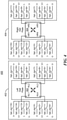
- magnetic field sensing element arrangement 400 including elements 302, 304 FIG.
- Switch arrays 402, 404 can form part of switching and amplification circuit 114 ( FIG. 1 ) and, in general, can be coupled between sensing elements 302, 304 and an amplifier (e.g., amplifier 316 in FIG. 3 ) and controlled in order to selectively couple sensing element terminals to inputs of the amplifier.
- First Hall effect sensing element 302 and second Hall effect sensing element 304 may generally be referred to as "left" and "right” elements, as shown in FIG. 4 , although this is meant to easily differentiate between the two different elements and does not necessarily imply a directionality of the elements.
- Signal hp1_sw ⁇ 15:0> may generally be a digital input signal to control switch array 402 for "left” element 302.
- Signal hpr_sw ⁇ 15:0> may generally be a digital input signal to control switch array 404 for "right” element 304.
- Each element 302 and 304 may have a positive and a negative analog output signal, which is selected by the respective switch arrays 402 and 404, from the respective "left” and “right” element terminals "HL1"-"HL4" and "HR1"-"HR4".
- Signals hpl_sw and hpr_sw may generally be provided to switch arrays 402 and 404 by digital controller 126 of FIG. 1 .
- V+ may represent the positive output signal of a given element
- V- may represent the negative output signal of a given element
- I+ may represent the positive bias input (current or voltage) of a given element
- I- may represent the negative bias input (current or voltage) of a given element.
- both elements 302, 304 have effectively the same or substantially similar sensitivity to magnetic fields.
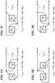
- Table 1 contains rows corresponding to different operational phases. Such phases refer to chopping phases in embodiments implementing chopping. Thus, in embodiments that do not implement chopping, only a single phase may be used. Table 1 illustrates a 4 phase chopping scheme and the Hall plate connections are illustrated in FIGs. 5A - 5D for respective phases 0 - 3.
- FIG. 5B V- I+ V+ I- V+ I+ V- I- 2 L-R 0010 0001 1000 0100 0010 0100 1000 0001
- FIG. 5C I- V- I+ V+ I- V+ I+ V- 3 -(L-R) 0100 0010 0001 1000 0001 0010 0100 1000
- FIG. 5D V+ I- V- I+ V- I- V+ I+
- FIGs. 5A-5D show output connections of a magnetic field sensor employing a chopping circuit in accordance with described embodiments, for example as shown in FIG. 4 and Table 1.
- FIG. 5A shows the connection of "left” and “right” Hall elements 302 and 304 for phase 0, as shown in Table 1.
- terminal HL2 of "left” Hall element 302 is coupled to "V+”
- terminal HL4 of "left” Hall element 302 is coupled to "V-”
- terminal HR2 of "right” Hall element 304 is coupled to "V-”
- terminal HR4 of "right” Hall element 304 is coupled to "V+”.
- Each Hall element is driven by an input current applied from terminal 1 (e.g., HL1 and HR1 are “I+”) to terminal 3 (e.g., HL3 and HR3 are "I-").
- terminal 1 e.g., HL1 and HR1 are "I+”
- terminal 3 e.g., HL3 and HR3 are "I-"
- the two Hall elements are concurrently or simultaneously driven with a current in the same direction through both elements, and with a current having the same phase.
- output signals of opposite polarity are coupled to each other, resulting in differential signals that subtract, thus cancelling the effect of stray fields and resulting in an output that is stray field immune.
- terminal HL2 is coupled to terminal HR4 to generate HOUTP (e.g., the positive differential output signal of the magnetic field sensor), and terminal HL4 is coupled to terminal HR2 to generate HOUTN (e.g., the negative differential output signal of the magnetic field sensor), resulting in an output voltage of the magnetic field sensor that is equal to the left sensing element signal minus the right sensing element signal (e.g., sig L -sig R ).
- HOUTP e.g., the positive differential output signal of the magnetic field sensor
- HOUTN e.g., the negative differential output signal of the magnetic field sensor
- FIG. 5B shows the connection of "left” and “right” Hall elements 302 and 304 for phase 1, as shown in Table 1.
- Table 1 shows that during phase 1, terminal HL3 of "left” Hall element 302 is coupled to “V+”, and terminal HL1 of “left” Hall element 302 is coupled to “V-”, while terminal HR3 of "right” Hall element 304 is coupled to "V-”, and terminal HR1 of "right” Hall element 304 is coupled to "V+”.
- Each Hall element is driven by an input current applied from terminal 2 (e.g., HL2 and HR2 are “I+”) to terminal 4 (e.g., HL4 and HR4 are "I-").
- the two Hall elements are concurrently or simultaneously driven with a current in the same direction through both elements, and with a current having the same phase.
- signals of opposite polarity are coupled to each other, resulting in differential signals that subtract, thus cancelling stray field signals and resulting in an output that is stray field immune.
- terminal HL3 is coupled to terminal HR1 to generate HOUTP (e.g., the positive differential output signal of the magnetic field sensor), and terminal HL1 is coupled to terminal HR3 to generate HOUTN (e.g., the negative differential output signal of the magnetic field sensor), resulting in an output voltage of the magnetic field sensor that is equal to the left sensing element signal less the right sensing element signal (e.g., -(sig L -sig R )).
- HOUTP e.g., the positive differential output signal of the magnetic field sensor
- HOUTN e.g., the negative differential output signal of the magnetic field sensor
- FIG. 5C shows the connection of "left” and “right” Hall elements 302 and 304 for phase 2, as shown in Table 1.
- Table 1 shows that during phase 2, terminal HL4 of "left” Hall element 302 is coupled to “V+”, and terminal HL2 of "left” Hall element 302 is coupled to “V-”, while terminal HR4 of "right” Hall element 304 is coupled to "V-”, and terminal HR2 of "right” Hall element 304 is coupled to "V+”.
- Each Hall element is driven by an input current applied from terminal 3 (e.g., HL3 and HR3 are “I+”) to terminal 1 (e.g., HL1 and HR1 are "I-").
- the two Hall elements are concurrently or simultaneously driven with a current in the same direction through both elements, and with a current having the same phase.
- signals of opposite polarity are coupled to each other, resulting in differential signals that subtract, thus cancelling stray field signals and resulting in an output that is stray field immune.
- terminal HL4 is coupled to terminal HR2 to generate HOUTP (e.g., the positive differential output signal of the magnetic field sensor), and terminal HL2 is coupled to terminal HR4 to generate HOUTN (e.g., the negative differential output signal of the magnetic field sensor), resulting in an output voltage of the magnetic field sensor that is equal to the left sensing element signal less the right sensing element signal (e.g., sig L -sig R ).
- HOUTP e.g., the positive differential output signal of the magnetic field sensor
- HOUTN e.g., the negative differential output signal of the magnetic field sensor
- FIG. 5D shows the connection of "left” and “right” Hall elements 302 and 304 for phase 3, as shown in Table 1.
- terminal HL1 of "left” Hall element 302 is coupled to “V+”
- terminal HL3 of "left” Hall element 302 is coupled to "V-”
- terminal HR1 of "right” Hall element 304 is coupled to "V-”
- terminal HR3 of "right” Hall element 304 is coupled to "V+”.
- Each Hall element is driven by an input current applied from terminal 4 (e.g., HL4 and HR4 are "I+”) to terminal 2 (e.g., HL2 and HR2 are "I-").
- the two Hall elements are concurrently or simultaneously driven with a current in the same direction through both elements, and with a current having the same phase.
- signals of opposite polarity are coupled to each other, resulting in differential signals that subtract, thus cancelling stray field signals and resulting in an output that is stray field immune.
- terminal HL1 is coupled to terminal HR3 to generate HOUTP (e.g., the positive differential output signal of the magnetic field sensor), and terminal HL3 is coupled to terminal HR1 to generate HOUTN (e.g., the negative differential output signal of the magnetic field sensor), resulting in an output voltage of the magnetic field sensor that is equal to the left sensing element signal less the right sensing element signal (e.g., -(sig L -sig R )).
- HOUTP e.g., the positive differential output signal of the magnetic field sensor
- HOUTN e.g., the negative differential output signal of the magnetic field sensor
- chopping may be employed to "rotate" through 2 or 4 of the phases shown in Table 1 to eliminate the offset signal (e.g., off L -off R ). Note that in each chopping phase shown in Table 1, the negative voltage output of one of the Hall elements is coupled to the positive of voltage output of the other Hall element, and vise-versa, thereby maintaining the stray field immunity benefits of the Hall plate configuration during chopping.
- FIG. 6 shows a block diagram of a signal processing path of a magnetic field sensor such as shown in FIG. 1 .
- magnetic field sensor system 600 includes two or more spaced magnetic field sensing elements 602 and 604, each spaced from the other by a predetermined distance, for sensing a magnetic field affected by a target (not shown in FIG. 6 ) and generating respective magnetic field signals 606 and 608.
- a modulator as may take the form of a switching module 610, is coupled to receive the first and second magnetic field signals 606 and 608 and is configured to generate a combined signal 612.
- Amplifier 614 is coupled to receive the combined signal 612 and generate amplified signal 616.
- Analog-to-digital converter (ADC) 618 may be provided to convert the amplified signal 616 into a digital signal 620.
- ADC Analog-to-digital converter
- Filter 622 is coupled to receive the digital signal 620 and generate an output signal 624.
- filter 622 is a low pass filter having a cutoff frequency less than or equal to a rate of the clock signal (CLK) and a zero at the frequency of the clock signal (CLK).
- CLK rate of the clock signal
- CLK clock signal
- CLK cascaded integrator-comb
- switched capacitor filter a switched capacitor filter.
- the magnetic field sensor 600 may be provided in the form of an integrated circuit in some embodiments.
- FIG. 7 shows an illustrative method 700 for sensing a magnetic field, for example using magnetic field sensor 100.
- process 700 begins.
- a bias current and/or bias voltage applied to each of the magnetic field sensing elements e.g., 110 and 112 of FIG. 1
- connection points may be selected for the magnetic field sensing elements, for example as described in regard to Table 1 and FIGs. 4 and 5A-5D .
- the selected currents and/or voltages are applied to both magnetic field sensing elements.
- the switch arrays connect the magnetic field sensing elements in parallel with opposite polarity to the amplifier as described in connection with FIG. 3 .
- the analog magnetic field sensing element output signals are combined and applied to the amplifier, which amplifies the combined analog signals and generates an output signal in which high frequency stray fields are rejected.
- chopping is optionally applied, for example by returning process 700 to block 706 to select new connection points for the magnetic field sensing elements, for example as described in regard to Table 1 and FIGs. 4 and 5A-5D .
- process 700 is complete. Alternatively, process 700 may continue to run, for example as long as system 100 is powered.
- embodiments provide a magnetic field sensor having a first magnetic field sensing element and a second magnetic field sensing element disposed at a predetermined distance from the first magnetic field sensing element.
- the first and second magnetic field sensing elements generate first and second magnetic field signals, respectively, that are indicative of a magnetic field associated with a target.
- a switching module couples the first magnetic field sensing element and the second magnetic field sensing element in parallel to an amplifier by coupling a first terminal of the first magnetic field sensing element having a first polarity to a first terminal of the second magnetic field sensing element having a polarity opposite the first polarity to generate a first combined signal, and coupling a second terminal of the first magnetic field sensing element having a polarity opposite the first polarity to a second terminal of the second magnetic field sensing element having the first polarity to generate a second combined signal.
- the switching module simultaneously couples the first combined signal and the second combined signal to the amplifier.
- the amplifier generates a magnetic field output signal indicative of the magnetic field associated with the target that has stray magnetic field effects cancelled.
- Some embodiments might be implemented in the form of methods and apparatuses for practicing those methods. Further, as would be apparent to one skilled in the art, various functions of circuit elements may be implemented as a software program. Described embodiments might be implemented in the form of program code embodied in tangible media, such as magnetic media, optical media, solid state memory, hard drives, or any other machine-readable storage medium, wherein, when the program code is loaded into and executed by a machine, such as a computer, the machine becomes an apparatus for practicing the method implemented by the program code.
- DSPs digital signal processors
- CPUs central processing units
- GPUs graphics processing units
- ASICs application specific integrated circuits
- FPGAs field programmable gate arrays
- the program code When implemented on one or more processors, including for example, one or more digital signal processors (DSPs), central processing units (CPUs), graphics processing units (GPUs), microcontrollers, application specific integrated circuits (ASICs), field programmable gate arrays (FPGAs), or general purpose computers, the program code combines with the processor(s) to provide a unique device that operates analogously to specific logic circuits.
- DSPs digital signal processors
- CPUs central processing units
- GPUs graphics processing units
- ASICs application specific integrated circuits
- FPGAs field programmable gate arrays
- general purpose computers the program code combines with the processor(s) to provide a unique device that operates analogously to specific logic circuits.
Landscapes
- Physics & Mathematics (AREA)
- Condensed Matter Physics & Semiconductors (AREA)
- General Physics & Mathematics (AREA)
- Measuring Magnetic Variables (AREA)
- Hall/Mr Elements (AREA)
Abstract
Description
- The present disclosure relates generally to magnetic field sensors and more specifically to such sensors having stray field rejection.
- Magnetic field sensors may employ one or more magnetic field sensing elements and are used in a variety of applications, including, but not limited to, a current sensor that senses a magnetic field generated by a current carried by a current-carrying conductor, a magnetic switch or proximity detector that senses proximity of a ferromagnetic or magnetic target object, a rotation detector that senses passing ferromagnetic articles, for example, gear teeth, and a magnetic field sensor that senses a magnetic field density of a magnetic field.
- Various magnetic field sensors may employ a variety of types of magnetic field sensing elements, including, but not limited to, Hall effect elements, magnetoresistance elements, and magnetotransistors. Hall effect elements generate an output voltage proportional to a magnetic field. It is known that Hall effect elements can exhibit an undesirable DC offset voltage. Further, some magnetic field sensors employ differential magnetic field sensing whereby spatially separated magnetic field sensing elements are used to generate a differential signal to reduce stray magnetic field effects.
- Described embodiments provide a magnetic field sensor having a first magnetic field sensing element and a second magnetic field sensing element disposed at a predetermined distance from the first magnetic field sensing element. The first and second magnetic field sensing elements generate first and second magnetic field signals, respectively, that are indicative of a magnetic field associated with a target. A switching module couples the first magnetic field sensing element and the second magnetic field sensing element in parallel to an amplifier by coupling a first terminal of the first magnetic field sensing element having a first polarity to a first terminal of the second magnetic field sensing element having a polarity opposite the first polarity to generate a first combined signal, and coupling a second terminal of the first magnetic field sensing element having a polarity opposite the first polarity to a second terminal of the second magnetic field sensing element having the first polarity to generate a second combined signal. The switching module simultaneously couples the first combined signal and the second combined signal to the amplifier. The amplifier generates a magnetic field output signal indicative of a difference between the first combined signal and the second combined signal. The difference is indicative of the magnetic field associated with the target that has stray magnetic field effects cancelled.
- Aspects provide that the switching module is one or more of: a switch matrix comprising a plurality of switches, and one or more multiplexers. The switching module can provide chopping to reduce a DC offset of the first magnetic field signal and the second magnetic field signal.
- Aspects provide that each of the first and second magnetic field sensing elements has four terminals, and the switching module includes a set of four switches for each terminal of the first and second magnetic field sensing elements, each set of four switches selectively coupling each terminal to one of a drive input signal having a positive polarity, a drive input signal having a negative polarity, an output signal having a positive polarity, and an output signal having a negative polarity. For the first magnetic field sensing element, a first terminal is coupled to the positive polarity drive input signal, a second terminal opposite the first terminal is coupled to the negative polarity drive input signal, a third terminal is coupled to the positive polarity output signal, and a fourth terminal is coupled to the negative polarity output signal. For the second magnetic field sensing element, a first terminal is coupled to the positive polarity drive input signal, a second terminal opposite the first terminal is coupled to the negative polarity drive input signal, a third terminal is coupled to the positive polarity output signal, and a fourth terminal is coupled to the negative polarity output signal.
- Aspects provide that, to perform chopping, the switching module selectively changes which of the four terminals of the first magnetic field sensing element is coupled to the positive polarity drive input signal, the negative polarity drive input signal, the positive polarity output signal, and the negative polarity output signal, and to selectively change which of the four terminals of the second magnetic field sensing element is coupled to the positive polarity drive input signal, the negative polarity drive input signal, the positive polarity output signal, and the negative polarity output signal, wherein the selective changing reduces a DC offset of the first and second combined signals. A clock module generates a clock signal, and the switching module provides chopping based upon the clock signal.
- Aspects provide that the switching module selectively provides chopping for one of: zero phases, two phases, and four phases. The switching module provides chopping for zero phases by not selectively changing which terminals of the first and second magnetic field sensing elements are coupled to the positive polarity drive input signal, the negative polarity drive input signal, the positive polarity output signal, and the negative polarity output signal. The switching module provides chopping for 2 phases (2X chopping) by selectively changing between a first set of terminal connections and a second set of terminal connections to the positive polarity drive input signal, the negative polarity drive input signal, the positive polarity output signal, and the negative polarity output signal. The switching module provides chopping for 4 phases (4X chopping) by selectively changing between a first set of terminal connections, a second set of terminal connections, a third set of terminal connections, and a fourth set of terminal connections to the positive polarity drive input signal, the negative polarity drive input signal, the positive polarity output signal, and the negative polarity output signal.
- Aspects provide that the switching module provides a determined drive signal to a selected terminal of each of the first and the second magnetic field sensing elements. The drive signal is one of a determined voltage and a determined current. Aspects provide that a controller coupled to the switching module generates a sensor output signal indicative of the magnetic field output signal. Aspects provide that the first and second magnetic field sensing elements are one or more Hall effect elements. Aspects provide that the magnetic field output signal is proportional to a difference between the first magnetic field signal and the second magnetic field signal.
- Another embodiment provides a method for sensing a magnetic field. A first magnetic field signal is generated with a first magnetic field sensing element, the first magnetic field signal indicative of a magnetic field associated with a target. A second magnetic field signal is generated with a second magnetic field sensing element spaced from the first magnetic field sensing element, the second magnetic field signal indicative of the magnetic field associated with the target. A magnetic field output signal indicative of the magnetic field is generated by coupling the first magnetic field sensing element and the second magnetic field sensing element in parallel to an amplifier by coupling a first terminal of the first magnetic field sensing element having a first polarity to a first terminal of the second magnetic field sensing element having a polarity opposite the first polarity and generating a first combined signal, and coupling a second terminal of the first magnetic field sensing element having a polarity opposite the first polarity to a second terminal of the second magnetic field sensing element having the first polarity and generating a second combined signal. The first combined signal and the second combined signal are simultaneously coupled to the amplifier. The magnetic field output signal is generated that is indicative of a difference between the first combined signal and the second combined signal that has stray magnetic field effects cancelled.
- Aspects provide chopping to reduce a DC offset of the first magnetic field signal and the second magnetic field signal. Aspects provide that each of the first and second magnetic field sensing elements has four terminals. A set of switches coupled to each terminal of the first magnetic field sensing element selectively couples a first terminal of the first magnetic field sensing element to a positive polarity drive input signal, a second terminal of the first magnetic field sensing element, opposite the first terminal, to a negative polarity drive input signal, a third terminal of the first magnetic field sensing element to a positive polarity output signal, and a fourth terminal of the first magnetic field sensing element, opposite the third terminal, to a negative polarity output signal. A set of switches coupled to each terminal of the second magnetic field sensing element selectively couples a first terminal of the second magnetic field sensing element to a positive polarity drive input signal, a second terminal of the second magnetic field sensing element, opposite the first terminal, to a negative polarity drive input signal, a third terminal of the second magnetic field sensing element to a positive polarity output signal, and a fourth terminal of the second magnetic field sensing element, opposite the third terminal, to a negative polarity output signal. Aspects selectively change which of the four terminals of the first magnetic field sensing element is coupled to the positive polarity drive input signal, the negative polarity drive input signal, the positive polarity output signal, and the negative polarity output signal, and to selectively change which of the four terminals of the second magnetic field sensing element is coupled to the positive polarity drive input signal, the negative polarity drive input signal, the positive polarity output signal, and the negative polarity output signal, wherein the selective changing reduces a DC offset of the first and second combined signals.
- Aspects provide that the chopping includes performing chopping for zero phases by not selectively changing which terminals of the first and second magnetic field sensing elements are coupled to the positive polarity drive input signal, the negative polarity drive input signal, the positive polarity output signal, and the negative polarity output signal. Aspects provide that the chopping includes performing chopping for 2 phases (2X chopping) by selectively changing between a first set of terminal connections and a second set of terminal connections to the positive polarity drive input signal, the negative polarity drive input signal, the positive polarity output signal, and the negative polarity output signal. Aspects provide that the chopping includes performing chopping for 4 phases (4X chopping) by selectively changing between a first set of terminal connections, a second set of terminal connections, a third set of terminal connections, and a fourth set of terminal connections to the positive polarity drive input signal, the negative polarity drive input signal, the positive polarity output signal, and the negative polarity output signal.
- Aspects provide a determined drive signal to a selected terminal of each of the first and the second magnetic field sensing elements. The drive signal is one of a determined voltage and a determined current. Aspects generate a sensor output signal indicative of the magnetic field output signal. Aspects provide that the first and second magnetic field sensing elements each comprise one or more Hall effect elements.
- Another embodiment provides a magnetic field sensor having a first magnetic field sensing element to generate a first magnetic field signal indicative of a magnetic field associated with a target, and a second magnetic field sensing element, disposed at a predetermined distance from the first magnetic field sensing element, to generate a second magnetic field signal indicative of the magnetic field associated with the target. The first magnetic field sensing element and the second magnetic field sensing element are coupled in parallel to an amplifier. A first terminal of the first magnetic field sensing element having a first polarity is coupled to a first terminal of the second magnetic field sensing element having a polarity opposite the first polarity to generate a first combined signal. A second terminal of the first magnetic field sensing element having a polarity opposite the first polarity is coupled to a second terminal of the second magnetic field sensing element having the first polarity to generate a second combined signal. The first combined signal and the second combined signal are provided to the amplifier, which generates a magnetic field output signal indicative of a difference between the first combined signal and the second combined signal. The difference is indicative of the magnetic field associated with the target that has stray magnetic field effects cancelled.
- Another embodiment provides a magnetic field sensor having first magnetic field sensing means to generate a first magnetic field signal indicative of a magnetic field associated with a target, and second magnetic field sensing means, disposed at a predetermined distance from the first magnetic field sensing means, to generate a second magnetic field signal indicative of the magnetic field associated with the target. Switching means couple the first magnetic field sensing means and the second magnetic field sensing means in parallel to amplification means. The switching means couples a first terminal of the first magnetic field sensing means having a first polarity to a first terminal of the second magnetic field sensing means having a polarity opposite the first polarity to generate a first combined signal. The switching means couples a second terminal of the first magnetic field sensing means having a polarity opposite the first polarity to a second terminal of the second magnetic field sensing means having the first polarity to generate a second combined signal. The switching means simultaneously couples the first combined signal and the second combined signal to the amplification means. The amplification means generates a magnetic field output signal indicative of a difference between the first combined signal and the second combined signal. The difference is indicative of the magnetic field associated with the target that has stray magnetic field effects cancelled.
- Another embodiment provides a magnetic field sensor having first magnetic field sensing means to generate a first magnetic field signal indicative of a magnetic field associated with a target and second magnetic field sensing means, disposed at a predetermined distance from the first magnetic field sensing means, to generate a second magnetic field signal indicative of the magnetic field associated with the target. The first magnetic field sensing means and the second magnetic field sensing means are coupled in parallel to amplification means. A first terminal of the first magnetic field sensing means having a first polarity is coupled to a first terminal of the second magnetic field sensing means having a polarity opposite the first polarity to generate a first combined signal. A second terminal of the first magnetic field sensing means having a polarity opposite the first polarity is coupled to a second terminal of the second magnetic field sensing means having the first polarity to generate a second combined signal. The first combined signal and the second combined signal are provided to the amplification means. The amplification means generates a magnetic field output signal indicative of a difference between the first combined signal and the second combined signal. The difference is indicative of the magnetic field associated with the target that has stray magnetic field effects cancelled.
- Other aspects, features, and advantages will become more fully apparent from the following detailed description, the appended claims, and the accompanying drawings in which like reference numerals identify similar or identical elements. Reference numerals that are introduced in the specification in association with a drawing figure may be repeated in one or more subsequent figures without additional description in the specification in order to provide context for other features.
-
FIG. 1 shows a block diagram of a magnetic field sensor in accordance with described embodiments; -
FIG. 2 shows an arrangement of Hall effect sensing elements of a magnetic field sensor in accordance with the prior art; -
FIG. 3 shows an arrangement of Hall effect sensing elements of a magnetic field sensor in accordance with described embodiments; -
FIG. 4 shows an illustrative schematic of a chopping circuit in accordance with described embodiments; -
FIGs. 5A, 5B, 5C, and 5D show output connections of a magnetic field sensor employing a chopping circuit in accordance with described embodiments; -
FIG. 6 shows an illustrative schematic of a magnetic field sensor circuit in accordance with described embodiments; and -
FIG. 7 shows a flow diagram of a technique of operating a magnetic field sensor in accordance with described embodiments. - In accordance with described embodiments, a magnetic field sensor is provided having a first magnetic field sensing element and a second magnetic field sensing element disposed at a predetermined distance from the first magnetic field sensing element. The first and second magnetic field sensing elements generate first and second magnetic field signals, respectively, that are indicative of a magnetic field associated with a target. A switching module couples the first magnetic field sensing element and the second magnetic field sensing element in parallel to an amplifier by coupling a first terminal of the first magnetic field sensing element having a first polarity to a first terminal of the second magnetic field sensing element having a polarity opposite the first polarity to generate a first combined signal, and coupling a second terminal of the first magnetic field sensing element having a polarity opposite the first polarity to a second terminal of the second magnetic field sensing element having the first polarity to generate a second combined signal. The switching module simultaneously couples the first combined signal and the second combined signal to the amplifier. The amplifier generates a magnetic field output signal indicative of the magnetic field associated with the target that has stray magnetic field effects cancelled.
- By way of introduction, as used herein, the term "magnetic field sensing element" describes a variety of types of electronic elements that sense a magnetic field. The magnetic field sensing elements can be, but are not limited to, Hall effect elements, magnetoresistance elements, or magnetotransistors. There are different types of Hall effect elements, for example, planar Hall elements, vertical Hall elements, and circular Hall elements. There are different types of magnetoresistance elements, for example, anisotropic magnetoresistance (AMR) elements, giant magnetoresistance (GMR) elements, tunneling magnetoresistance (TMR) elements, Indium antimonide (InSb) elements, and magnetic tunnel junction (MTJ) elements. Most, but not all, types of magnetoresistance elements tend to have axes of maximum sensitivity parallel to a substrate that supports the magnetic field sensing element and most, but not all, types of Hall elements tend to have axes of sensitivity perpendicular to a substrate that supports the magnetic field sensing element.
- As used herein, the term "magnetic field sensor" describes a circuit that includes one or more magnetic field sensing elements. Magnetic field sensors are used in a variety of applications, including, but not limited to, a current sensor that senses a magnetic field generated by a current carried by a current-carrying conductor, a magnetic switch or proximity detector that senses the proximity of a ferromagnetic or magnetic object, a rotation detector that senses passing ferromagnetic articles, for example, gear teeth, and a magnetic field sensor that senses a magnetic field density of a magnetic field. In general, the circuits and techniques described herein apply to any magnetic field sensor capable of detecting a magnetic field.
-
FIG. 1 shows a block diagram of a magnetic field sensor, shown asmagnetic field sensor 100. In described embodiments,magnetic field sensor 100 may be a magnetic angle and linear position sensing integrated circuit for consumer, industrial, and automotive applications.Magnetic field sensor 100 may employ various types of magneticfield sensing elements target 160. In some embodiments,target 160 may be a magnetic element. In other embodiments,target 160 may be a ferromagnetic element that affects a magnetic field when positioned in proximity to a magnet 170 (e.g., a back-biased configuration). In some embodiments,magnetic field sensor 100 may be provided as an integrated circuit. - As shown in
FIG. 1 ,magnetic field sensor 100 may include analog front end (AFE) 102 anddigital system 104.Power system 106 may receive one or more input voltages (shown as voltage signal VCC inFIG. 1 ) and a ground or common signal (shown as GND signal inFIG. 1 ).Power system 106 may provide power signals (e.g., one or more voltages) toAFE 102 anddigital system 104, as well as to one or moreother sensors 108. In some embodiments,other sensors 108 may include one or more additional sensors to sense conditions ofmagnetic field sensor 100 and/or the environment in whichmagnetic field sensor 100 is deployed, for example one or more temperature sensors for use to compensate sensitivity and/or offset ofmagnetic field sensor 100 over temperature. - In some embodiments,
AFE 102 may include a plurality of magnetic field sensing elements, shown asHall effect elements -
Hall effect elements amplification circuit 114, which is described in greater detail in regard toFIG. 4 . As shown,Hall effect elements magnetic field signals amplification circuit 114. In some embodiments, one or more amplifiers may amplify the signals output fromHall effect elements - Switching and
amplification circuit 114 may provide combinedanalog output signal 140 to analog-to-digital converter (ADC) 116, which converts combinedanalog output signal 140 intodigital output signal 142, which in turn is provided todigital system 104. As will be described,digital system 104 may process the receiveddigital signal 142 and, in response, generate one or more output signals frommagnetic field sensor 100. For example, in some embodiments,magnetic field sensor 100 may be in communication with an engine control unit (ECU) of a vehicle, or other control unit in a system in whichmagnetic field sensor 100 is deployed, via one or more signals received by or transmitted from magnetic field sensor 100 (e.g., SENT/PWM signal shown inFIG. 1 ). - In some embodiments,
elements output signals field sensing elements amplification circuit 114 such that any effects from stray magnetic fields experienced by both sensing elements (i.e., common to both elements) tend to cancel in the resulting differentialmagnetic field signal 140, whereas the field that is desired to be detected can be readily detectable from the resulting differential magnetic field signal. - In some embodiments, each magnetic
field sensing element elements elements elements - As will be described in greater detail in regard to
FIGs. 3 ,4 and5 , switching andamplification circuit 114 is configured to selectively coupleelements analog output signal 140. In such embodiments, switching andamplification circuit 114 couples drive signals to selected terminals of eachelement elements amplification circuit 114 may be configured to couple analog output signals from each element such that the output signal from one of the elements has an inverted polarity with respect to the output signal from the other element. The two analog output signals may be directly combined to form a combinedanalog output signal 140 that has cancelled the effects from stray magnetic signals (e.g., common mode effects). As will be described, this may allow use of only a single amplifier to generate the combined analog output signal, rather than processing the output of each element separately. Additionally, by directly combining the output signals of the elements in the analog domain, more complex circuitry and/or processing algorithms can be avoided. - Additionally, as will be described in greater detail in regard to
FIGs. 4 and5 , in some embodiments, to reduce DC offset of the Hall effect elements, "chopping" or "current spinning" may be employed. Chopping refers to driving a Hall effect element in two or more different directions by changing which sensing element terminals are coupled to power and ground connections and receiving output signals at different terminals as the Hall effect element is differently driven. In such embodiments, switching andamplification circuit 114 may also receive clock signal(s) fromclock module 124 and/or control signal(s) fromcontroller 126. In this way, selected drive and output signal contact pairs are interchanged during each phase of the chopping and offset voltages tend to cancel. Thus, in described embodiments, switching andamplification circuit 114 may achieve both DC offset reduction and stray effect cancellation formagnetic field sensor 100. - As shown in
FIG. 1 ,digital system 104 may includefiltering module 118 that is coupled to receivedigital signal 142 fromADC 116. In described embodiments,filtering module 118 may be a low pass filter having various forms including, but not limited to, a cascaded integrator-comb (CIC) decimation filter or a switched capacitor filter.Digital system 104 may also includeclock module 124, which is coupled to, and provides one or more clock signals to,controller 126. In described embodiments,controller 126 is coupled to receive filtered magneticfield output signal 144 fromfilter module 118 and, in response, is configured to generate a sensor output signal as may be transmitted by SENT/PWM transmitter 130 ofcommunication interface 134. For example,controller 126 may provide signal(s) to SENT/PWM transmitter 130 to generate an output signal ofmagnetic field sensor 100 to be transmitted to an external device coupled tomagnetic field sensor 100, such as an ECU (not shown). The SENT/PWM output signal is generally indicative of an output of the magneticfield sensing elements - As shown in
FIG. 1 , SENT/PWM signal may be a bidirectional communication signal to send and receive data to/from devices external tomagnetic field sensor 100, such as an ECU.Serial receiver 136 may receive signals and provide received data tocontroller 126. In some embodiments,serial receiver 136 may decode Manchester encoded serial data and provide a received signal tocontroller 126.Controller 126 may adjust operation ofmagnetic field sensor 100 in response to a received signal, or may transmit a response via SENT/PWM transmitter 130.Controller 126 may also be coupled tomemory 122, which may store data associated with operation ofmagnetic field sensor 100, for example past values of the SENT/PWM output signal, past data output fromelements 110 and 112 (e.g., past values of filtered magnetic field output signal 144), data received (e.g., received from an ECU), variable settings for operation ofmagnetic field sensor 100, and so forth. Further, in some embodiments,controller 126 might be configured to adjust biasing or trimming ofelements - It will be appreciated that while
communication interface 134 is described as transmitting and receiving a SENT and/or PWM formatted signal, other signal formats are possible for communicating sensor information including, but not limited to, I2C, SPI (serial peripheral interface), and A/B/I format. -
FIG. 2 shows a block diagram of a conventional magnetic fieldsensing element arrangement 200. As shown, in a conventional system, two magnetic field sensing elements (e.g., Hall effect elements) 202 and 204 might be employed to detect a magnetic field. As shown, each Halleffect sensing element signals 206 and 208) are coupled toamplifier 210, and two contacts from Hall effect sensing element 204 (shown assignals 214 and 216) are coupled toamplifier 218. As shown, one input for each ofamplifiers amplifiers Amplifiers output signals field output signal 222.Amplifiers outputs effect sensing elements - Thus, as shown in
FIG. 2 , a conventional system includes two dedicated amplifiers (210, 218) that are coupled to Halleffect sensing elements amplifiers magnetic field signal 222. Such a system requires twoamplifiers -
FIG. 3 shows a block diagram of a magnetic fieldsensing element arrangement 300 in accordance with described embodiments. As will be described, some embodiments provide an arrangement for magnetic field sensing elements that determines an analog difference of magnetic fields sensed by the magnetic field sensing elements, which achieves improved stray field immunity, particularly for high frequency stray fields. Some embodiments may also provide a signal chopping scheme to reduce or eliminate DC offset. - As shown in
FIG. 3 , a described embodiment may include two magnetic field sensing elements (e.g., Hall effect sensing elements) 302 and 304 to detect a magnetic field. As shown, each Halleffect sensing element signal 311. Another contact from Hall effect sensing element 302 (shown assignal 308, having the opposite polarity of signal 306) is coupled to an opposite polarity contact from Hall effect sensing element 304 (shown as signal 312) to generate combinedsignal 313. Combinedsignals amplifier 316 to generate adifference signal 314. The Hall elements are concurrently or simultaneously driven with a current in the same direction through both elements, and with a current having the same phase. However, output signals of opposite polarity are coupled to each other. With this arrangement, the field effects common to both elements (such as stray fields) cancel, thereby resulting in an output that is stray field immune. A differential field (the field desired to be detected) has the same polarity for each of the two Hall effect elements, and thus the output signal resulting from theconfiguration 300 will be one-half of the drive voltage level. - Thus, as shown in
FIG. 3 , described embodiments include only oneamplifier 316 coupled to Halleffect sensing elements difference signal 314 in the analog domain by connecting the magnetic field sensor output signals in a particular manner, and then processing the combinedsignals difference signal 314. Advantages of such embodiments over conventional systems include a capability of rejecting high frequency stray field immunity without needing to employ complex ADC and/or DSP, lower cost, lower power consumption, and smaller physical size due to only employing one amplifier, and having the only source of signal error be due to Hall effect sensing element sensitivity mismatch, which can be compensated. Referring also toFIG. 4 , magnetic fieldsensing element arrangement 400 includingelements 302, 304 (FIG. 3 ) is shown to be coupled to respective switch networks orarrays Switch arrays FIG. 1 ) and, in general, can be coupled betweensensing elements amplifier 316 inFIG. 3 ) and controlled in order to selectively couple sensing element terminals to inputs of the amplifier. First Halleffect sensing element 302 and second Halleffect sensing element 304 may generally be referred to as "left" and "right" elements, as shown inFIG. 4 , although this is meant to easily differentiate between the two different elements and does not necessarily imply a directionality of the elements. - Table 1 below illustrates control of switches within the
switch arrays switch array 402 for "left"element 302. Signal hpr_sw <15:0> may generally be a digital input signal to controlswitch array 404 for "right"element 304. Eachelement respective switch arrays arrays digital controller 126 ofFIG. 1 . As shown in Table 1, "V+" may represent the positive output signal of a given element, "V-" may represent the negative output signal of a given element, and "I+" may represent the positive bias input (current or voltage) of a given element, and "I-" may represent the negative bias input (current or voltage) of a given element. In a desirable embodiment, bothelements - Table 1 contains rows corresponding to different operational phases. Such phases refer to chopping phases in embodiments implementing chopping. Thus, in embodiments that do not implement chopping, only a single phase may be used. Table 1 illustrates a 4 phase chopping scheme and the Hall plate connections are illustrated in
FIGs. 5A - 5D for respective phases 0 - 3.Table 1 Phase (figure) Output Left plate switch <15:0> Right plate switch <15:0> <15:12> <11:8> <7:4> <3:0> <15:12> <11:8> <7:4> <3:0> HL1 HL2 HL3 HL4 HR1 HR2 HR3 HR4 0 L-R 1000 0100 0010 0001 1000 0001 0010 0100 FIG. 5A I+ V+ I- V- I+ V- I- V+ 1 -(L-R) 0001 1000 0100 0010 0100 1000 0001 0010 FIG. 5B V- I+ V+ I- V+ I+ V- I- 2 L-R 0010 0001 1000 0100 0010 0100 1000 0001 FIG. 5C I- V- I+ V+ I- V+ I+ V- 3 -(L-R) 0100 0010 0001 1000 0001 0010 0100 1000 FIG. 5D V+ I- V- I+ V- I- V+ I+ -
FIGs. 5A-5D show output connections of a magnetic field sensor employing a chopping circuit in accordance with described embodiments, for example as shown inFIG. 4 and Table 1. For example,FIG. 5A shows the connection of "left" and "right"Hall elements phase 0, as shown in Table 1. As shown in Table 1, duringphase 0, terminal HL2 of "left"Hall element 302 is coupled to "V+", and terminal HL4 of "left"Hall element 302 is coupled to "V-", while terminal HR2 of "right"Hall element 304 is coupled to "V-", and terminal HR4 of "right"Hall element 304 is coupled to "V+". Each Hall element is driven by an input current applied from terminal 1 (e.g., HL1 and HR1 are "I+") to terminal 3 (e.g., HL3 and HR3 are "I-"). Thus, as shown, the two Hall elements are concurrently or simultaneously driven with a current in the same direction through both elements, and with a current having the same phase. However, output signals of opposite polarity are coupled to each other, resulting in differential signals that subtract, thus cancelling the effect of stray fields and resulting in an output that is stray field immune. Thus, as shown inFIG. 5A , terminal HL2 is coupled to terminal HR4 to generate HOUTP (e.g., the positive differential output signal of the magnetic field sensor), and terminal HL4 is coupled to terminal HR2 to generate HOUTN (e.g., the negative differential output signal of the magnetic field sensor), resulting in an output voltage of the magnetic field sensor that is equal to the left sensing element signal minus the right sensing element signal (e.g., sigL-sigR). The subtraction of the differential signals occurs by reversing the polarity of one plate relative to the other. -
FIG. 5B shows the connection of "left" and "right"Hall elements phase 1, as shown in Table 1. As shown in Table 1, duringphase 1, terminal HL3 of "left"Hall element 302 is coupled to "V+", and terminal HL1 of "left"Hall element 302 is coupled to "V-", while terminal HR3 of "right"Hall element 304 is coupled to "V-", and terminal HR1 of "right"Hall element 304 is coupled to "V+". Each Hall element is driven by an input current applied from terminal 2 (e.g., HL2 and HR2 are "I+") to terminal 4 (e.g., HL4 and HR4 are "I-"). Thus, as shown, the two Hall elements are concurrently or simultaneously driven with a current in the same direction through both elements, and with a current having the same phase. However, signals of opposite polarity are coupled to each other, resulting in differential signals that subtract, thus cancelling stray field signals and resulting in an output that is stray field immune. Thus, as shown inFIG. 5B , terminal HL3 is coupled to terminal HR1 to generate HOUTP (e.g., the positive differential output signal of the magnetic field sensor), and terminal HL1 is coupled to terminal HR3 to generate HOUTN (e.g., the negative differential output signal of the magnetic field sensor), resulting in an output voltage of the magnetic field sensor that is equal to the left sensing element signal less the right sensing element signal (e.g., -(sigL-sigR)). The subtraction of the differential signals occurs by reversing the polarity of one plate relative to the other. -
FIG. 5C shows the connection of "left" and "right"Hall elements phase 2, as shown in Table 1. As shown in Table 1, duringphase 2, terminal HL4 of "left"Hall element 302 is coupled to "V+", and terminal HL2 of "left"Hall element 302 is coupled to "V-", while terminal HR4 of "right"Hall element 304 is coupled to "V-", and terminal HR2 of "right"Hall element 304 is coupled to "V+". Each Hall element is driven by an input current applied from terminal 3 (e.g., HL3 and HR3 are "I+") to terminal 1 (e.g., HL1 and HR1 are "I-"). Thus, as shown, the two Hall elements are concurrently or simultaneously driven with a current in the same direction through both elements, and with a current having the same phase. However, signals of opposite polarity are coupled to each other, resulting in differential signals that subtract, thus cancelling stray field signals and resulting in an output that is stray field immune. Thus, as shown inFIG. 5C , terminal HL4 is coupled to terminal HR2 to generate HOUTP (e.g., the positive differential output signal of the magnetic field sensor), and terminal HL2 is coupled to terminal HR4 to generate HOUTN (e.g., the negative differential output signal of the magnetic field sensor), resulting in an output voltage of the magnetic field sensor that is equal to the left sensing element signal less the right sensing element signal (e.g., sigL-sigR). The subtraction of the differential signals occurs by reversing the polarity of one plate relative to the other. -
FIG. 5D shows the connection of "left" and "right"Hall elements phase 3, as shown in Table 1. As shown in Table 1, duringphase 3, terminal HL1 of "left"Hall element 302 is coupled to "V+", and terminal HL3 of "left"Hall element 302 is coupled to "V-", while terminal HR1 of "right"Hall element 304 is coupled to "V-", and terminal HR3 of "right"Hall element 304 is coupled to "V+". Each Hall element is driven by an input current applied from terminal 4 (e.g., HL4 and HR4 are "I+") to terminal 2 (e.g., HL2 and HR2 are "I-"). Thus, as shown, the two Hall elements are concurrently or simultaneously driven with a current in the same direction through both elements, and with a current having the same phase. However, signals of opposite polarity are coupled to each other, resulting in differential signals that subtract, thus cancelling stray field signals and resulting in an output that is stray field immune. Thus, as shown inFIG. 5D , terminal HL1 is coupled to terminal HR3 to generate HOUTP (e.g., the positive differential output signal of the magnetic field sensor), and terminal HL3 is coupled to terminal HR1 to generate HOUTN (e.g., the negative differential output signal of the magnetic field sensor), resulting in an output voltage of the magnetic field sensor that is equal to the left sensing element signal less the right sensing element signal (e.g., -(sigL-sigR)). The subtraction of the differential signals occurs by reversing the polarity of one plate relative to the other. - As shown in
FIGs. 5A-5D , in embodiments where DC offset is an important consideration, chopping may be employed to "rotate" through 2 or 4 of the phases shown in Table 1 to eliminate the offset signal (e.g., offL-offR). Note that in each chopping phase shown in Table 1, the negative voltage output of one of the Hall elements is coupled to the positive of voltage output of the other Hall element, and vise-versa, thereby maintaining the stray field immunity benefits of the Hall plate configuration during chopping. -
FIG. 6 shows a block diagram of a signal processing path of a magnetic field sensor such as shown inFIG. 1 . As shown inFIG. 6 , magneticfield sensor system 600 includes two or more spaced magneticfield sensing elements FIG. 6 ) and generating respective magnetic field signals 606 and 608. A modulator, as may take the form of aswitching module 610, is coupled to receive the first and second magnetic field signals 606 and 608 and is configured to generate a combinedsignal 612.Amplifier 614 is coupled to receive the combinedsignal 612 and generate amplifiedsignal 616. Analog-to-digital converter (ADC) 618 may be provided to convert the amplifiedsignal 616 into adigital signal 620. -
Filter 622 is coupled to receive thedigital signal 620 and generate anoutput signal 624. In some embodiments,filter 622 is a low pass filter having a cutoff frequency less than or equal to a rate of the clock signal (CLK) and a zero at the frequency of the clock signal (CLK). Various forms and types of low pass filters are possible including, but not limited to a cascaded integrator-comb (CIC) decimation filter or a switched capacitor filter. Themagnetic field sensor 600 may be provided in the form of an integrated circuit in some embodiments. -
FIG. 7 shows anillustrative method 700 for sensing a magnetic field, for example usingmagnetic field sensor 100. Atblock 702,process 700 begins. Atblock 704, a bias current and/or bias voltage applied to each of the magnetic field sensing elements (e.g., 110 and 112 ofFIG. 1 ) may optionally be adjusted, for example to adjust a DC offset of the magnetic field sensing elements. Atblock 706, when chopping is being employed, connection points may be selected for the magnetic field sensing elements, for example as described in regard to Table 1 andFIGs. 4 and5A-5D . Atblock 708, the selected currents and/or voltages are applied to both magnetic field sensing elements. Atblock 710, the switch arrays connect the magnetic field sensing elements in parallel with opposite polarity to the amplifier as described in connection withFIG. 3 . Atblock 712, the analog magnetic field sensing element output signals are combined and applied to the amplifier, which amplifies the combined analog signals and generates an output signal in which high frequency stray fields are rejected. Atblock 714, chopping is optionally applied, for example by returningprocess 700 to block 706 to select new connection points for the magnetic field sensing elements, for example as described in regard to Table 1 andFIGs. 4 and5A-5D . Atblock 718,process 700 is complete. Alternatively,process 700 may continue to run, for example as long assystem 100 is powered. - Thus, as described herein, embodiments provide a magnetic field sensor having a first magnetic field sensing element and a second magnetic field sensing element disposed at a predetermined distance from the first magnetic field sensing element. The first and second magnetic field sensing elements generate first and second magnetic field signals, respectively, that are indicative of a magnetic field associated with a target. A switching module couples the first magnetic field sensing element and the second magnetic field sensing element in parallel to an amplifier by coupling a first terminal of the first magnetic field sensing element having a first polarity to a first terminal of the second magnetic field sensing element having a polarity opposite the first polarity to generate a first combined signal, and coupling a second terminal of the first magnetic field sensing element having a polarity opposite the first polarity to a second terminal of the second magnetic field sensing element having the first polarity to generate a second combined signal. The switching module simultaneously couples the first combined signal and the second combined signal to the amplifier. The amplifier generates a magnetic field output signal indicative of the magnetic field associated with the target that has stray magnetic field effects cancelled.
- Reference herein to "one embodiment" or "an embodiment" means that a particular feature, structure, or characteristic described in connection with the embodiment can be included in at least one embodiment of the claimed subject matter. The appearances of the phrase "in one embodiment" in various places in the specification are not necessarily all referring to the same embodiment, nor are separate or alternative embodiments necessarily mutually exclusive of other embodiments. The same applies to the term "implementation."
- Some embodiments might be implemented in the form of methods and apparatuses for practicing those methods. Further, as would be apparent to one skilled in the art, various functions of circuit elements may be implemented as a software program. Described embodiments might be implemented in the form of program code embodied in tangible media, such as magnetic media, optical media, solid state memory, hard drives, or any other machine-readable storage medium, wherein, when the program code is loaded into and executed by a machine, such as a computer, the machine becomes an apparatus for practicing the method implemented by the program code. When implemented on one or more processors, including for example, one or more digital signal processors (DSPs), central processing units (CPUs), graphics processing units (GPUs), microcontrollers, application specific integrated circuits (ASICs), field programmable gate arrays (FPGAs), or general purpose computers, the program code combines with the processor(s) to provide a unique device that operates analogously to specific logic circuits.
- It should be understood that the steps of the illustrative methods set forth herein are not necessarily required to be performed in the order described. Likewise, additional steps may be included in such methods, and certain steps may be omitted or combined, in methods consistent with various embodiments.
- It will be further understood that various changes in the details, materials, and arrangements of the parts which have been described and illustrated in order to explain the nature of the described embodiments might be made by those skilled in the art without departing from the scope of the following claims.
Claims (20)
- A magnetic field sensor comprising:a first magnetic field sensing element configured to generate a first magnetic field signal indicative of a magnetic field associated with a target;a second magnetic field sensing element, disposed at a predetermined distance from the first magnetic field sensing element, configured to generate a second magnetic field signal indicative of the magnetic field associated with the target; anda switching module configured to couple the first magnetic field sensing element and the second magnetic field sensing element in parallel to an amplifier, the switching module configured to:couple a first terminal of the first magnetic field sensing element having a first polarity to a first terminal of the second magnetic field sensing element having a polarity opposite the first polarity to generate a first combined signal;couple a second terminal of the first magnetic field sensing element having a polarity opposite the first polarity to a second terminal of the second magnetic field sensing element having the first polarity to generate a second combined signal; andsimultaneously couple the first combined signal and the second combined signal to the amplifier, the amplifier configured to generate a magnetic field output signal indicative of a difference between the first combined signal and the second combined signal, wherein the difference is indicative of the magnetic field associated with the target that has stray magnetic field effects cancelled.
- The magnetic field sensor of claim 1, wherein the switching module comprises one or more of: a switch matrix comprising a plurality of switches, and one or more multiplexers.
- The magnetic field sensor of claim 2, wherein the switching module is further configured to provide chopping to reduce a DC offset of the first magnetic field signal and the second magnetic field signal.
- The magnetic field sensor of claim 3, wherein each of the first and second magnetic field sensing elements has four terminals, and wherein the switching module comprises:a set of four switches for each terminal of the first and second magnetic field sensing elements, each set of four switches configured to selectively couple each terminal to one of a drive input signal having a positive polarity, a drive input signal having a negative polarity, an output signal having a positive polarity, and an output signal having a negative polarity,wherein, for the first magnetic field sensing element, a first terminal is coupled to the positive polarity drive input signal, a second terminal opposite the first terminal is coupled to the negative polarity drive input signal, a third terminal is coupled to the positive polarity output signal, and a fourth terminal is coupled to the negative polarity output signal, andwherein, for the second magnetic field sensing element, a first terminal is coupled to the positive polarity drive input signal, a second terminal opposite the first terminal is coupled to the negative polarity drive input signal, a third terminal is coupled to the positive polarity output signal, and a fourth terminal is coupled to the negative polarity output signal.
- The magnetic field sensor of claim 4, wherein, to provide chopping, the switching module is configured to selectively change which of the four terminals of the first magnetic field sensing element is coupled to the positive polarity drive input signal, the negative polarity drive input signal, the positive polarity output signal, and the negative polarity output signal, and to selectively change which of the four terminals of the second magnetic field sensing element is coupled to the positive polarity drive input signal, the negative polarity drive input signal, the positive polarity output signal, and the negative polarity output signal, wherein the selective changing reduces a DC offset of the first and second combined signals.
- The magnetic field sensor of claim 5, further comprising a clock module configured to generate a clock signal, and wherein the switching module is configured to provide chopping based upon the clock signal.
- The magnetic field sensor of claim 5, wherein the switching module is configured to selectively provide chopping for one of:zero phases by not selectively changing which terminals of the first and second magnetic field sensing elements are coupled to the positive polarity drive input signal, the negative polarity drive input signal, the positive polarity output signal, and the negative polarity output signal;2 phases (2X chopping) by selectively changing between a first set of terminal connections and a second set of terminal connections to the positive polarity drive input signal, the negative polarity drive input signal, the positive polarity output signal, and the negative polarity output signal; and4 phases (4X chopping) by selectively changing between a first set of terminal connections, a second set of terminal connections, a third set of terminal connections, and a fourth set of terminal connections to the positive polarity drive input signal, the negative polarity drive input signal, the positive polarity output signal, and the negative polarity output signal.
- The magnetic field sensor of claim 1, wherein the switching module is further configured to provide a determined drive signal to a selected terminal of each of the first and the second magnetic field sensing elements.
- The magnetic field sensor of claim 1, further comprising a controller coupled to the switching module and configured to generate a sensor output signal indicative of the magnetic field output signal.
- The magnetic field sensor of claim 1, wherein the magnetic field output signal is proportional to a difference between the first magnetic field signal and the second magnetic field signal.
- A method for sensing a magnetic field, the method comprising:generating a first magnetic field signal with a first magnetic field sensing element, the first magnetic field signal indicative of a magnetic field associated with a target;generating a second magnetic field signal with a second magnetic field sensing element spaced from the first magnetic field sensing element, the second magnetic field signal indicative of the magnetic field associated with the target;generating a magnetic field output signal indicative of the magnetic field by coupling the first magnetic field sensing element and the second magnetic field sensing element in parallel to an amplifier, the coupling comprising:coupling a first terminal of the first magnetic field sensing element having a first polarity to a first terminal of the second magnetic field sensing element having a polarity opposite the first polarity and generating a first combined signal;coupling a second terminal of the first magnetic field sensing element having a polarity opposite the first polarity to a second terminal of the second magnetic field sensing element having the first polarity and generating a second combined signal;simultaneously coupling the first combined signal and the second combined signal to the amplifier; andgenerating the magnetic field output signal, wherein the magnetic field output signal is indicative of a difference between the first combined signal and the second combined signal that has stray magnetic field effects cancelled.
- The method of claim 11, further comprising:
providing chopping to reduce a DC offset of the first magnetic field signal and the second magnetic field signal. - The method of claim 12, wherein each of the first and second magnetic field sensing elements has four terminals, the method further comprising:selectively coupling, by a set of switches coupled to each terminal of the first magnetic field sensing element, a first terminal of the first magnetic field sensing element to a positive polarity drive input signal, a second terminal of the first magnetic field sensing element, opposite the first terminal, to a negative polarity drive input signal, a third terminal of the first magnetic field sensing element to a positive polarity output signal, and a fourth terminal of the first magnetic field sensing element, opposite the third terminal, to a negative polarity output signal; andselectively coupling, by a set of switches coupled to each terminal of the second magnetic field sensing element, a first terminal of the second magnetic field sensing element to a positive polarity drive input signal, a second terminal of the second magnetic field sensing element, opposite the first terminal, to a negative polarity drive input signal, a third terminal of the second magnetic field sensing element to a positive polarity output signal, and a fourth terminal of the second magnetic field sensing element, opposite the third terminal, to a negative polarity output signal.
- The method of claim 13, further comprising:
selectively changing which of the four terminals of the first magnetic field sensing element is coupled to the positive polarity drive input signal, the negative polarity drive input signal, the positive polarity output signal, and the negative polarity output signal, and to selectively change which of the four terminals of the second magnetic field sensing element is coupled to the positive polarity drive input signal, the negative polarity drive input signal, the positive polarity output signal, and the negative polarity output signal, wherein the selective changing reduces a DC offset of the first and second combined signals. - The method of claim 14, wherein the chopping comprises one of:performing chopping for zero phases by not selectively changing which terminals of the first and second magnetic field sensing elements are coupled to the positive polarity drive input signal, the negative polarity drive input signal, the positive polarity output signal, and the negative polarity output signal;performing chopping for 2 phases (2X chopping) by selectively changing between a first set of terminal connections and a second set of terminal connections to the positive polarity drive input signal, the negative polarity drive input signal, the positive polarity output signal, and the negative polarity output signal; andperforming chopping for 4 phases (4X chopping) by selectively changing between a first set of terminal connections, a second set of terminal connections, a third set of terminal connections, and a fourth set of terminal connections to the positive polarity drive input signal, the negative polarity drive input signal, the positive polarity output signal, and the negative polarity output signal.
- The method of claim 11, further comprising:
providing a determined drive signal to a selected terminal of each of the first and the second magnetic field sensing elements. - The method of claim 16, or the magnetic field sensor of claim 8, wherein the drive signal is one of a determined voltage and a determined current.
- The method of claim 11, further comprising:
generating a sensor output signal indicative of the magnetic field output signal. - The method of claim 11, or the magnetic field sensor of claim 1, wherein the first and second magnetic field sensing elements each comprise one or more Hall effect elements.
- A magnetic field sensor comprising:a first magnetic field sensing element configured to generate a first magnetic field signal indicative of a magnetic field associated with a target;a second magnetic field sensing element, disposed at a predetermined distance from the first magnetic field sensing element, configured to generate a second magnetic field signal indicative of the magnetic field associated with the target;wherein the first magnetic field sensing element and the second magnetic field sensing element are coupled in parallel to an amplifier, wherein:a first terminal of the first magnetic field sensing element having a first polarity is coupled to a first terminal of the second magnetic field sensing element having a polarity opposite the first polarity to generate a first combined signal;a second terminal of the first magnetic field sensing element having a polarity opposite the first polarity is coupled to a second terminal of the second magnetic field sensing element having the first polarity to generate a second combined signal; andthe first combined signal and the second combined signal are provided to the amplifier, the amplifier configured to generate a magnetic field output signal indicative of a difference between the first combined signal and the second combined signal, wherein the difference is indicative of the magnetic field associated with the target that has stray magnetic field effects cancelled.
Applications Claiming Priority (1)
| Application Number | Priority Date | Filing Date | Title |
|---|---|---|---|
| US16/985,577 US11163019B1 (en) | 2020-08-05 | 2020-08-05 | Magnetic field sensors having stray field rejection |
Publications (2)
| Publication Number | Publication Date |
|---|---|
| EP3951415A1 true EP3951415A1 (en) | 2022-02-09 |
| EP3951415B1 EP3951415B1 (en) | 2025-10-08 |
Family
ID=77226685
Family Applications (1)
| Application Number | Title | Priority Date | Filing Date |
|---|---|---|---|
| EP21189847.3A Active EP3951415B1 (en) | 2020-08-05 | 2021-08-05 | Magnetic field sensors having stray field rejection |
Country Status (2)
| Country | Link |
|---|---|
| US (1) | US11163019B1 (en) |
| EP (1) | EP3951415B1 (en) |
Families Citing this family (6)
| Publication number | Priority date | Publication date | Assignee | Title |
|---|---|---|---|---|
| EP3457154B1 (en) | 2017-09-13 | 2020-04-08 | Melexis Technologies SA | Stray field rejection in magnetic sensors |
| US12416692B2 (en) | 2020-09-09 | 2025-09-16 | Allegro Microsystems, Llc | Stray field immune angle sensor |
| US11940505B2 (en) * | 2021-05-28 | 2024-03-26 | The Board Of Trustees Of The Leland Stanford Junior University | Omega and theta—a method to measure magnetic field at AC frequencies without using current spinning |
| US11953395B2 (en) | 2022-03-18 | 2024-04-09 | Allegro Microsystems, Llc | Magnetic field differential linear torque sensor |
| US12140646B2 (en) * | 2023-02-06 | 2024-11-12 | Allegro Microsystems, Llc | Magnetic sensing having hall plate routing to reduce inductive coupling |
| US12644936B2 (en) | 2023-09-12 | 2026-06-02 | Allegro Microsystems, Llc | Chopping scheme for magnetic field sensor having shared ADC |
Citations (4)
| Publication number | Priority date | Publication date | Assignee | Title |
|---|---|---|---|---|
| US20120274314A1 (en) * | 2011-04-27 | 2012-11-01 | Allegro Microsystems, Inc. | Circuits and Methods for Self-Calibrating or Self-Testing a Magnetic Field Sensor |
| US20140361766A1 (en) * | 2012-02-01 | 2014-12-11 | Ams Ag | Hall sensor and sensor arrangement |
| US20190302196A1 (en) * | 2018-03-27 | 2019-10-03 | Allegro Microsystems, Llc | Magnetic field sensor and associated methods including differential chopping |
| US20200241082A1 (en) * | 2019-01-28 | 2020-07-30 | Melexis Technologies Sa | Bridge sensor with dummy resistor structure |
Family Cites Families (11)
| Publication number | Priority date | Publication date | Assignee | Title |
|---|---|---|---|---|
| US6984978B2 (en) * | 2002-02-11 | 2006-01-10 | Honeywell International Inc. | Magnetic field sensor |
| US7164263B2 (en) * | 2004-01-16 | 2007-01-16 | Fieldmetrics, Inc. | Current sensor |
| US7425821B2 (en) * | 2006-10-19 | 2008-09-16 | Allegro Microsystems, Inc. | Chopped Hall effect sensor |
| JP4884299B2 (en) | 2007-05-18 | 2012-02-29 | 旭化成エレクトロニクス株式会社 | Magnetic detector |
| US7605647B1 (en) | 2008-04-29 | 2009-10-20 | Allegro Microsystems, Inc. | Chopper-stabilized amplifier and magnetic field sensor |
| EP2634592B1 (en) | 2009-07-22 | 2015-01-14 | Allegro Microsystems, LLC | Circuits and methods for generating a diagnostic mode of operation in a magnetic field sensor |
| CN103080755B (en) * | 2010-08-31 | 2015-01-21 | 阿尔卑斯绿色器件株式会社 | Current sensor |
| US9201122B2 (en) | 2012-02-16 | 2015-12-01 | Allegro Microsystems, Llc | Circuits and methods using adjustable feedback for self-calibrating or self-testing a magnetic field sensor with an adjustable time constant |
| US9354123B2 (en) | 2012-12-26 | 2016-05-31 | Allegro Microsystems, Llc | Systems and methods for processing temperature data or other signals |
| GB201315964D0 (en) | 2013-09-06 | 2013-10-23 | Melexis Technologies Nv | Magnetic field orientation sensor and angular position sensor using same |
| US10120041B2 (en) * | 2015-03-27 | 2018-11-06 | Allegro Microsystems, Llc | Magnetic field sensor |
-
2020
- 2020-08-05 US US16/985,577 patent/US11163019B1/en active Active
-
2021
- 2021-08-05 EP EP21189847.3A patent/EP3951415B1/en active Active
Patent Citations (4)
| Publication number | Priority date | Publication date | Assignee | Title |
|---|---|---|---|---|
| US20120274314A1 (en) * | 2011-04-27 | 2012-11-01 | Allegro Microsystems, Inc. | Circuits and Methods for Self-Calibrating or Self-Testing a Magnetic Field Sensor |
| US20140361766A1 (en) * | 2012-02-01 | 2014-12-11 | Ams Ag | Hall sensor and sensor arrangement |
| US20190302196A1 (en) * | 2018-03-27 | 2019-10-03 | Allegro Microsystems, Llc | Magnetic field sensor and associated methods including differential chopping |
| US20200241082A1 (en) * | 2019-01-28 | 2020-07-30 | Melexis Technologies Sa | Bridge sensor with dummy resistor structure |
Also Published As
| Publication number | Publication date |
|---|---|
| US11163019B1 (en) | 2021-11-02 |
| EP3951415B1 (en) | 2025-10-08 |
Similar Documents
| Publication | Publication Date | Title |
|---|---|---|
| EP3951415B1 (en) | Magnetic field sensors having stray field rejection | |
| US10866289B2 (en) | Magnetic field sensor and associated methods including differential chopping | |
| EP3457088B1 (en) | Reducing ripple generated from chopper stabilization | |
| JP6045592B2 (en) | Magnetic field sensing element combining circular vertical Hall magnetic field sensing element and planar Hall element | |
| US10782366B2 (en) | Multi-channel sensor output signal protocols | |
| US20190312579A1 (en) | Magnetic field sensor with switching network | |
| CN114264861A (en) | Current sensor | |
| KR101109712B1 (en) | Magnetism sensor | |
| EP2071348B1 (en) | Magnetic detector | |
| US11630130B2 (en) | Channel sensitivity matching | |
| CN102313831A (en) | Current sensor | |
| CN108418560A (en) | Readout Method Applied to Hall Current Sensor | |
| US10498198B2 (en) | Magnetic sensor | |
| US20090012733A1 (en) | Offset correction program and electronic compass | |
| JP4904358B2 (en) | Magnetic detector | |
| JPWO2008099662A1 (en) | Magnetic detector | |
| US20220155387A1 (en) | Magnetic field sensor with stacked transducers and capacitive summing amplifier | |
| US9684042B2 (en) | Magnetic field sensor with improved accuracy and method of obtaining improved accuracy with a magnetic field sensor | |
| EP2088446A1 (en) | Magnetic detector and electronic device | |
| WO2008075610A1 (en) | Magnetic detector | |
| JP7651767B1 (en) | Magnetic Sensors | |
| US12306214B2 (en) | Adjustable sensitivity ranges for magnetic field sensors | |
| JPH06216432A (en) | Magnetic flux density detector | |
| JPS5820014A (en) | Amplifying circuit |
Legal Events
| Date | Code | Title | Description |
|---|---|---|---|
| PUAI | Public reference made under article 153(3) epc to a published international application that has entered the european phase |
Free format text: ORIGINAL CODE: 0009012 |
|
| STAA | Information on the status of an ep patent application or granted ep patent |
Free format text: STATUS: THE APPLICATION HAS BEEN PUBLISHED |
|
| AK | Designated contracting states |
Kind code of ref document: A1 Designated state(s): AL AT BE BG CH CY CZ DE DK EE ES FI FR GB GR HR HU IE IS IT LI LT LU LV MC MK MT NL NO PL PT RO RS SE SI SK SM TR |
|
| STAA | Information on the status of an ep patent application or granted ep patent |
Free format text: STATUS: REQUEST FOR EXAMINATION WAS MADE |
|
| 17P | Request for examination filed |
Effective date: 20220808 |
|
| RBV | Designated contracting states (corrected) |
Designated state(s): AL AT BE BG CH CY CZ DE DK EE ES FI FR GB GR HR HU IE IS IT LI LT LU LV MC MK MT NL NO PL PT RO RS SE SI SK SM TR |
|
| STAA | Information on the status of an ep patent application or granted ep patent |
Free format text: STATUS: EXAMINATION IS IN PROGRESS |
|
| 17Q | First examination report despatched |
Effective date: 20240916 |
|
| GRAP | Despatch of communication of intention to grant a patent |
Free format text: ORIGINAL CODE: EPIDOSNIGR1 |
|
| STAA | Information on the status of an ep patent application or granted ep patent |
Free format text: STATUS: GRANT OF PATENT IS INTENDED |
|
| INTG | Intention to grant announced |
Effective date: 20250605 |
|
| GRAS | Grant fee paid |
Free format text: ORIGINAL CODE: EPIDOSNIGR3 |
|
| GRAA | (expected) grant |
Free format text: ORIGINAL CODE: 0009210 |
|
| STAA | Information on the status of an ep patent application or granted ep patent |
Free format text: STATUS: THE PATENT HAS BEEN GRANTED |
|
| AK | Designated contracting states |
Kind code of ref document: B1 Designated state(s): AL AT BE BG CH CY CZ DE DK EE ES FI FR GB GR HR HU IE IS IT LI LT LU LV MC MK MT NL NO PL PT RO RS SE SI SK SM TR |
|
| REG | Reference to a national code |
Ref country code: GB Ref legal event code: FG4D Ref country code: CH Ref legal event code: F10 Free format text: ST27 STATUS EVENT CODE: U-0-0-F10-F00 (AS PROVIDED BY THE NATIONAL OFFICE) Effective date: 20251008 |
|
| REG | Reference to a national code |
Ref country code: DE Ref legal event code: R096 Ref document number: 602021039945 Country of ref document: DE |
|
| REG | Reference to a national code |
Ref country code: IE Ref legal event code: FG4D |
|
| REG | Reference to a national code |
Ref country code: NL Ref legal event code: MP Effective date: 20251008 |
|
| REG | Reference to a national code |
Ref country code: AT Ref legal event code: MK05 Ref document number: 1845231 Country of ref document: AT Kind code of ref document: T Effective date: 20251008 |
|
| PG25 | Lapsed in a contracting state [announced via postgrant information from national office to epo] |
Ref country code: NL Free format text: LAPSE BECAUSE OF FAILURE TO SUBMIT A TRANSLATION OF THE DESCRIPTION OR TO PAY THE FEE WITHIN THE PRESCRIBED TIME-LIMIT Effective date: 20251008 |
|
| PG25 | Lapsed in a contracting state [announced via postgrant information from national office to epo] |
Ref country code: ES Free format text: LAPSE BECAUSE OF FAILURE TO SUBMIT A TRANSLATION OF THE DESCRIPTION OR TO PAY THE FEE WITHIN THE PRESCRIBED TIME-LIMIT Effective date: 20251008 |
|
| REG | Reference to a national code |
Ref country code: LT Ref legal event code: MG9D |
|
| PG25 | Lapsed in a contracting state [announced via postgrant information from national office to epo] |
Ref country code: NO Free format text: LAPSE BECAUSE OF FAILURE TO SUBMIT A TRANSLATION OF THE DESCRIPTION OR TO PAY THE FEE WITHIN THE PRESCRIBED TIME-LIMIT Effective date: 20260108 |
|
| PG25 | Lapsed in a contracting state [announced via postgrant information from national office to epo] |
Ref country code: AT Free format text: LAPSE BECAUSE OF FAILURE TO SUBMIT A TRANSLATION OF THE DESCRIPTION OR TO PAY THE FEE WITHIN THE PRESCRIBED TIME-LIMIT Effective date: 20251008 Ref country code: HR Free format text: LAPSE BECAUSE OF FAILURE TO SUBMIT A TRANSLATION OF THE DESCRIPTION OR TO PAY THE FEE WITHIN THE PRESCRIBED TIME-LIMIT Effective date: 20251008 Ref country code: FI Free format text: LAPSE BECAUSE OF FAILURE TO SUBMIT A TRANSLATION OF THE DESCRIPTION OR TO PAY THE FEE WITHIN THE PRESCRIBED TIME-LIMIT Effective date: 20251008 |
|
| PG25 | Lapsed in a contracting state [announced via postgrant information from national office to epo] |
Ref country code: RS Free format text: LAPSE BECAUSE OF FAILURE TO SUBMIT A TRANSLATION OF THE DESCRIPTION OR TO PAY THE FEE WITHIN THE PRESCRIBED TIME-LIMIT Effective date: 20260108 |
|
| PG25 | Lapsed in a contracting state [announced via postgrant information from national office to epo] |
Ref country code: IS Free format text: LAPSE BECAUSE OF FAILURE TO SUBMIT A TRANSLATION OF THE DESCRIPTION OR TO PAY THE FEE WITHIN THE PRESCRIBED TIME-LIMIT Effective date: 20260208 |
|
| PG25 | Lapsed in a contracting state [announced via postgrant information from national office to epo] |
Ref country code: PT Free format text: LAPSE BECAUSE OF FAILURE TO SUBMIT A TRANSLATION OF THE DESCRIPTION OR TO PAY THE FEE WITHIN THE PRESCRIBED TIME-LIMIT Effective date: 20260209 |
|
| PG25 | Lapsed in a contracting state [announced via postgrant information from national office to epo] |
Ref country code: PL Free format text: LAPSE BECAUSE OF FAILURE TO SUBMIT A TRANSLATION OF THE DESCRIPTION OR TO PAY THE FEE WITHIN THE PRESCRIBED TIME-LIMIT Effective date: 20251008 |
|
| PG25 | Lapsed in a contracting state [announced via postgrant information from national office to epo] |
Ref country code: LV Free format text: LAPSE BECAUSE OF FAILURE TO SUBMIT A TRANSLATION OF THE DESCRIPTION OR TO PAY THE FEE WITHIN THE PRESCRIBED TIME-LIMIT Effective date: 20251008 |
|
| PG25 | Lapsed in a contracting state [announced via postgrant information from national office to epo] |
Ref country code: BG Free format text: LAPSE BECAUSE OF FAILURE TO SUBMIT A TRANSLATION OF THE DESCRIPTION OR TO PAY THE FEE WITHIN THE PRESCRIBED TIME-LIMIT Effective date: 20251008 |
|
| PG25 | Lapsed in a contracting state [announced via postgrant information from national office to epo] |
Ref country code: LT Free format text: LAPSE BECAUSE OF FAILURE TO SUBMIT A TRANSLATION OF THE DESCRIPTION OR TO PAY THE FEE WITHIN THE PRESCRIBED TIME-LIMIT Effective date: 20251008 |
|
| PG25 | Lapsed in a contracting state [announced via postgrant information from national office to epo] |
Ref country code: SM Free format text: LAPSE BECAUSE OF FAILURE TO SUBMIT A TRANSLATION OF THE DESCRIPTION OR TO PAY THE FEE WITHIN THE PRESCRIBED TIME-LIMIT Effective date: 20251008 |
|
| PG25 | Lapsed in a contracting state [announced via postgrant information from national office to epo] |
Ref country code: DK Free format text: LAPSE BECAUSE OF FAILURE TO SUBMIT A TRANSLATION OF THE DESCRIPTION OR TO PAY THE FEE WITHIN THE PRESCRIBED TIME-LIMIT Effective date: 20251008 |
|
| PG25 | Lapsed in a contracting state [announced via postgrant information from national office to epo] |
Ref country code: IT Free format text: LAPSE BECAUSE OF FAILURE TO SUBMIT A TRANSLATION OF THE DESCRIPTION OR TO PAY THE FEE WITHIN THE PRESCRIBED TIME-LIMIT Effective date: 20251008 |
|
| PG25 | Lapsed in a contracting state [announced via postgrant information from national office to epo] |
Ref country code: EE Free format text: LAPSE BECAUSE OF FAILURE TO SUBMIT A TRANSLATION OF THE DESCRIPTION OR TO PAY THE FEE WITHIN THE PRESCRIBED TIME-LIMIT Effective date: 20251008 |
|
| PG25 | Lapsed in a contracting state [announced via postgrant information from national office to epo] |
Ref country code: CZ Free format text: LAPSE BECAUSE OF FAILURE TO SUBMIT A TRANSLATION OF THE DESCRIPTION OR TO PAY THE FEE WITHIN THE PRESCRIBED TIME-LIMIT Effective date: 20251008 |
|
| PG25 | Lapsed in a contracting state [announced via postgrant information from national office to epo] |
Ref country code: SK Free format text: LAPSE BECAUSE OF FAILURE TO SUBMIT A TRANSLATION OF THE DESCRIPTION OR TO PAY THE FEE WITHIN THE PRESCRIBED TIME-LIMIT Effective date: 20251008 |
|
| PG25 | Lapsed in a contracting state [announced via postgrant information from national office to epo] |
Ref country code: SE Free format text: LAPSE BECAUSE OF FAILURE TO SUBMIT A TRANSLATION OF THE DESCRIPTION OR TO PAY THE FEE WITHIN THE PRESCRIBED TIME-LIMIT Effective date: 20251008 |
|
| PLBE | No opposition filed within time limit |
Free format text: ORIGINAL CODE: 0009261 |
|
| STAA | Information on the status of an ep patent application or granted ep patent |
Free format text: STATUS: NO OPPOSITION FILED WITHIN TIME LIMIT |