EP3945588A2 - Pixel isolation structure - Google Patents
Pixel isolation structure Download PDFInfo
- Publication number
- EP3945588A2 EP3945588A2 EP21188180.0A EP21188180A EP3945588A2 EP 3945588 A2 EP3945588 A2 EP 3945588A2 EP 21188180 A EP21188180 A EP 21188180A EP 3945588 A2 EP3945588 A2 EP 3945588A2
- Authority
- EP
- European Patent Office
- Prior art keywords
- isolation
- substrate
- segment
- dummy
- image sensor
- Prior art date
- Legal status (The legal status is an assumption and is not a legal conclusion. Google has not performed a legal analysis and makes no representation as to the accuracy of the status listed.)
- Withdrawn
Links
- 238000002955 isolation Methods 0.000 title claims abstract description 215
- 239000000758 substrate Substances 0.000 claims abstract description 209
- 229910052751 metal Inorganic materials 0.000 claims abstract description 74
- 239000002184 metal Substances 0.000 claims abstract description 74
- 239000002131 composite material Substances 0.000 claims description 5
- 238000000034 method Methods 0.000 description 53
- 239000007769 metal material Substances 0.000 description 19
- 239000000463 material Substances 0.000 description 18
- 238000005137 deposition process Methods 0.000 description 13
- VYPSYNLAJGMNEJ-UHFFFAOYSA-N Silicium dioxide Chemical compound O=[Si]=O VYPSYNLAJGMNEJ-UHFFFAOYSA-N 0.000 description 11
- 239000004065 semiconductor Substances 0.000 description 11
- 229920002120 photoresistant polymer Polymers 0.000 description 10
- 238000000151 deposition Methods 0.000 description 9
- 238000000231 atomic layer deposition Methods 0.000 description 8
- 238000005229 chemical vapour deposition Methods 0.000 description 8
- 238000005240 physical vapour deposition Methods 0.000 description 8
- WFKWXMTUELFFGS-UHFFFAOYSA-N tungsten Chemical compound [W] WFKWXMTUELFFGS-UHFFFAOYSA-N 0.000 description 7
- 229910052721 tungsten Inorganic materials 0.000 description 7
- 239000010937 tungsten Substances 0.000 description 7
- 229910052581 Si3N4 Inorganic materials 0.000 description 6
- 239000010949 copper Substances 0.000 description 6
- 238000009713 electroplating Methods 0.000 description 6
- HQVNEWCFYHHQES-UHFFFAOYSA-N silicon nitride Chemical compound N12[Si]34N5[Si]62N3[Si]51N64 HQVNEWCFYHHQES-UHFFFAOYSA-N 0.000 description 6
- 238000004544 sputter deposition Methods 0.000 description 6
- RYGMFSIKBFXOCR-UHFFFAOYSA-N Copper Chemical compound [Cu] RYGMFSIKBFXOCR-UHFFFAOYSA-N 0.000 description 5
- 229910052802 copper Inorganic materials 0.000 description 5
- 238000000059 patterning Methods 0.000 description 5
- 235000012239 silicon dioxide Nutrition 0.000 description 5
- 239000000377 silicon dioxide Substances 0.000 description 5
- 238000010586 diagram Methods 0.000 description 4
- 239000003989 dielectric material Substances 0.000 description 4
- 239000010936 titanium Substances 0.000 description 4
- XUIMIQQOPSSXEZ-UHFFFAOYSA-N Silicon Chemical compound [Si] XUIMIQQOPSSXEZ-UHFFFAOYSA-N 0.000 description 3
- RTAQQCXQSZGOHL-UHFFFAOYSA-N Titanium Chemical compound [Ti] RTAQQCXQSZGOHL-UHFFFAOYSA-N 0.000 description 3
- 230000003667 anti-reflective effect Effects 0.000 description 3
- 238000005498 polishing Methods 0.000 description 3
- 229910052710 silicon Inorganic materials 0.000 description 3
- 239000010703 silicon Substances 0.000 description 3
- 229910052719 titanium Inorganic materials 0.000 description 3
- BOTDANWDWHJENH-UHFFFAOYSA-N Tetraethyl orthosilicate Chemical compound CCO[Si](OCC)(OCC)OCC BOTDANWDWHJENH-UHFFFAOYSA-N 0.000 description 2
- 229910052782 aluminium Inorganic materials 0.000 description 2
- XAGFODPZIPBFFR-UHFFFAOYSA-N aluminium Chemical compound [Al] XAGFODPZIPBFFR-UHFFFAOYSA-N 0.000 description 2
- 239000011651 chromium Substances 0.000 description 2
- 238000009792 diffusion process Methods 0.000 description 2
- 239000010931 gold Substances 0.000 description 2
- 229910000449 hafnium oxide Inorganic materials 0.000 description 2
- WIHZLLGSGQNAGK-UHFFFAOYSA-N hafnium(4+);oxygen(2-) Chemical compound [O-2].[O-2].[Hf+4] WIHZLLGSGQNAGK-UHFFFAOYSA-N 0.000 description 2
- TWNQGVIAIRXVLR-UHFFFAOYSA-N oxo(oxoalumanyloxy)alumane Chemical compound O=[Al]O[Al]=O TWNQGVIAIRXVLR-UHFFFAOYSA-N 0.000 description 2
- 230000005855 radiation Effects 0.000 description 2
- 239000010948 rhodium Substances 0.000 description 2
- VYZAMTAEIAYCRO-UHFFFAOYSA-N Chromium Chemical compound [Cr] VYZAMTAEIAYCRO-UHFFFAOYSA-N 0.000 description 1
- XEEYBQQBJWHFJM-UHFFFAOYSA-N Iron Chemical compound [Fe] XEEYBQQBJWHFJM-UHFFFAOYSA-N 0.000 description 1
- ZOKXTWBITQBERF-UHFFFAOYSA-N Molybdenum Chemical compound [Mo] ZOKXTWBITQBERF-UHFFFAOYSA-N 0.000 description 1
- KJTLSVCANCCWHF-UHFFFAOYSA-N Ruthenium Chemical compound [Ru] KJTLSVCANCCWHF-UHFFFAOYSA-N 0.000 description 1
- BQCADISMDOOEFD-UHFFFAOYSA-N Silver Chemical compound [Ag] BQCADISMDOOEFD-UHFFFAOYSA-N 0.000 description 1
- 230000004075 alteration Effects 0.000 description 1
- WPPDFTBPZNZZRP-UHFFFAOYSA-N aluminum copper Chemical compound [Al].[Cu] WPPDFTBPZNZZRP-UHFFFAOYSA-N 0.000 description 1
- 230000015572 biosynthetic process Effects 0.000 description 1
- 229910052804 chromium Inorganic materials 0.000 description 1
- 229910017052 cobalt Inorganic materials 0.000 description 1
- 239000010941 cobalt Substances 0.000 description 1
- GUTLYIVDDKVIGB-UHFFFAOYSA-N cobalt atom Chemical compound [Co] GUTLYIVDDKVIGB-UHFFFAOYSA-N 0.000 description 1
- 230000000295 complement effect Effects 0.000 description 1
- 238000010276 construction Methods 0.000 description 1
- PCHJSUWPFVWCPO-UHFFFAOYSA-N gold Chemical compound [Au] PCHJSUWPFVWCPO-UHFFFAOYSA-N 0.000 description 1
- 229910052737 gold Inorganic materials 0.000 description 1
- 238000005468 ion implantation Methods 0.000 description 1
- 238000004519 manufacturing process Methods 0.000 description 1
- 229910052750 molybdenum Inorganic materials 0.000 description 1
- 239000011733 molybdenum Substances 0.000 description 1
- 230000003287 optical effect Effects 0.000 description 1
- 229910052703 rhodium Inorganic materials 0.000 description 1
- MHOVAHRLVXNVSD-UHFFFAOYSA-N rhodium atom Chemical compound [Rh] MHOVAHRLVXNVSD-UHFFFAOYSA-N 0.000 description 1
- 229910052707 ruthenium Inorganic materials 0.000 description 1
- HBMJWWWQQXIZIP-UHFFFAOYSA-N silicon carbide Chemical compound [Si+]#[C-] HBMJWWWQQXIZIP-UHFFFAOYSA-N 0.000 description 1
- 229910010271 silicon carbide Inorganic materials 0.000 description 1
- 229910052814 silicon oxide Inorganic materials 0.000 description 1
- 229910052709 silver Inorganic materials 0.000 description 1
- 239000004332 silver Substances 0.000 description 1
- 239000000126 substance Substances 0.000 description 1
- 238000006467 substitution reaction Methods 0.000 description 1
Images






Classifications
-
- H—ELECTRICITY
- H10—SEMICONDUCTOR DEVICES; ELECTRIC SOLID-STATE DEVICES NOT OTHERWISE PROVIDED FOR
- H10F—INORGANIC SEMICONDUCTOR DEVICES SENSITIVE TO INFRARED RADIATION, LIGHT, ELECTROMAGNETIC RADIATION OF SHORTER WAVELENGTH OR CORPUSCULAR RADIATION
- H10F39/00—Integrated devices, or assemblies of multiple devices, comprising at least one element covered by group H10F30/00, e.g. radiation detectors comprising photodiode arrays
- H10F39/80—Constructional details of image sensors
- H10F39/805—Coatings
- H10F39/8057—Optical shielding
-
- H—ELECTRICITY
- H10—SEMICONDUCTOR DEVICES; ELECTRIC SOLID-STATE DEVICES NOT OTHERWISE PROVIDED FOR
- H10F—INORGANIC SEMICONDUCTOR DEVICES SENSITIVE TO INFRARED RADIATION, LIGHT, ELECTROMAGNETIC RADIATION OF SHORTER WAVELENGTH OR CORPUSCULAR RADIATION
- H10F39/00—Integrated devices, or assemblies of multiple devices, comprising at least one element covered by group H10F30/00, e.g. radiation detectors comprising photodiode arrays
- H10F39/011—Manufacture or treatment of image sensors covered by group H10F39/12
-
- H—ELECTRICITY
- H10—SEMICONDUCTOR DEVICES; ELECTRIC SOLID-STATE DEVICES NOT OTHERWISE PROVIDED FOR
- H10F—INORGANIC SEMICONDUCTOR DEVICES SENSITIVE TO INFRARED RADIATION, LIGHT, ELECTROMAGNETIC RADIATION OF SHORTER WAVELENGTH OR CORPUSCULAR RADIATION
- H10F39/00—Integrated devices, or assemblies of multiple devices, comprising at least one element covered by group H10F30/00, e.g. radiation detectors comprising photodiode arrays
- H10F39/011—Manufacture or treatment of image sensors covered by group H10F39/12
- H10F39/024—Manufacture or treatment of image sensors covered by group H10F39/12 of coatings or optical elements
-
- H—ELECTRICITY
- H10—SEMICONDUCTOR DEVICES; ELECTRIC SOLID-STATE DEVICES NOT OTHERWISE PROVIDED FOR
- H10F—INORGANIC SEMICONDUCTOR DEVICES SENSITIVE TO INFRARED RADIATION, LIGHT, ELECTROMAGNETIC RADIATION OF SHORTER WAVELENGTH OR CORPUSCULAR RADIATION
- H10F39/00—Integrated devices, or assemblies of multiple devices, comprising at least one element covered by group H10F30/00, e.g. radiation detectors comprising photodiode arrays
- H10F39/80—Constructional details of image sensors
- H10F39/806—Optical elements or arrangements associated with the image sensors
-
- H—ELECTRICITY
- H10—SEMICONDUCTOR DEVICES; ELECTRIC SOLID-STATE DEVICES NOT OTHERWISE PROVIDED FOR
- H10F—INORGANIC SEMICONDUCTOR DEVICES SENSITIVE TO INFRARED RADIATION, LIGHT, ELECTROMAGNETIC RADIATION OF SHORTER WAVELENGTH OR CORPUSCULAR RADIATION
- H10F39/00—Integrated devices, or assemblies of multiple devices, comprising at least one element covered by group H10F30/00, e.g. radiation detectors comprising photodiode arrays
- H10F39/80—Constructional details of image sensors
- H10F39/807—Pixel isolation structures
-
- H—ELECTRICITY
- H10—SEMICONDUCTOR DEVICES; ELECTRIC SOLID-STATE DEVICES NOT OTHERWISE PROVIDED FOR
- H10F—INORGANIC SEMICONDUCTOR DEVICES SENSITIVE TO INFRARED RADIATION, LIGHT, ELECTROMAGNETIC RADIATION OF SHORTER WAVELENGTH OR CORPUSCULAR RADIATION
- H10F39/00—Integrated devices, or assemblies of multiple devices, comprising at least one element covered by group H10F30/00, e.g. radiation detectors comprising photodiode arrays
- H10F39/80—Constructional details of image sensors
- H10F39/811—Interconnections
-
- H—ELECTRICITY
- H10—SEMICONDUCTOR DEVICES; ELECTRIC SOLID-STATE DEVICES NOT OTHERWISE PROVIDED FOR
- H10F—INORGANIC SEMICONDUCTOR DEVICES SENSITIVE TO INFRARED RADIATION, LIGHT, ELECTROMAGNETIC RADIATION OF SHORTER WAVELENGTH OR CORPUSCULAR RADIATION
- H10F39/00—Integrated devices, or assemblies of multiple devices, comprising at least one element covered by group H10F30/00, e.g. radiation detectors comprising photodiode arrays
- H10F39/10—Integrated devices
- H10F39/12—Image sensors
- H10F39/199—Back-illuminated image sensors
-
- H—ELECTRICITY
- H10—SEMICONDUCTOR DEVICES; ELECTRIC SOLID-STATE DEVICES NOT OTHERWISE PROVIDED FOR
- H10F—INORGANIC SEMICONDUCTOR DEVICES SENSITIVE TO INFRARED RADIATION, LIGHT, ELECTROMAGNETIC RADIATION OF SHORTER WAVELENGTH OR CORPUSCULAR RADIATION
- H10F39/00—Integrated devices, or assemblies of multiple devices, comprising at least one element covered by group H10F30/00, e.g. radiation detectors comprising photodiode arrays
- H10F39/80—Constructional details of image sensors
- H10F39/806—Optical elements or arrangements associated with the image sensors
- H10F39/8063—Microlenses
-
- H—ELECTRICITY
- H10—SEMICONDUCTOR DEVICES; ELECTRIC SOLID-STATE DEVICES NOT OTHERWISE PROVIDED FOR
- H10F—INORGANIC SEMICONDUCTOR DEVICES SENSITIVE TO INFRARED RADIATION, LIGHT, ELECTROMAGNETIC RADIATION OF SHORTER WAVELENGTH OR CORPUSCULAR RADIATION
- H10F39/00—Integrated devices, or assemblies of multiple devices, comprising at least one element covered by group H10F30/00, e.g. radiation detectors comprising photodiode arrays
- H10F39/80—Constructional details of image sensors
- H10F39/806—Optical elements or arrangements associated with the image sensors
- H10F39/8067—Reflectors
Definitions
- CMOS image sensors are used in a wide range of modern day electronic devices, such as, for example, cameras and cell phones.
- CMOS image sensors have begun to see widespread use, largely replacing charge-coupled device (CCD) image sensors.
- CCD image sensors charge-coupled device
- CMOS image sensors are favored due to low power consumption, small size, fast data processing, a direct output of data, and low manufacturing cost.
- CMOS image sensors include front-side illuminated (FSI) image sensors and back-side illuminated (BSI) image sensors.
- FSI front-side illuminated
- BSI back-side illuminated
- first and second features are formed in direct contact
- additional features may be formed between the first and second features, such that the first and second features may not be in direct contact
- present disclosure may repeat reference numerals and/or letters in the various examples. This repetition is for the purpose of simplicity and clarity and does not in itself dictate a relationship between the various embodiments and/or configurations discussed.
- spatially relative terms such as “beneath,” “below,” “lower,” “above,” “upper” and the like, may be used herein for ease of description to describe one element or feature's relationship to another element(s) or feature(s) as illustrated in the figures.
- the spatially relative terms are intended to encompass different orientations of the device in use or operation in addition to the orientation depicted in the figures.
- the apparatus may be otherwise oriented (rotated 90 degrees or at other orientations) and the spatially relative descriptors used herein may likewise be interpreted accordingly.
- An image sensor may include a semiconductor substrate and a metal interconnect structure disposed on a front side of the substrate. Further, the image sensor may include a plurality of pixels. Each pixel includes a photodetector in the semiconductor substrate. Further, the pixels are separated from each other by a shallow trench isolation (STI) structure disposed in the front side of the substrate and a deep trench isolation (DTI) structure disposed in a back side of substrate opposite the front side.
- the DTI structure and the STI structure may be arranged along a common vertical axis. Further, the DTI structure and the STI structure may together extend vertically through the substrate at boundaries of the pixels to separate the pixels. As a result, photons entering a portion of a substrate corresponding to a pixel may be confined to the portion and prevented from entering other portions of the substrate corresponding to neighboring pixels.
- a challenge with the image sensor is that while the DTI and STI structures may separate the pixels at the substrate, the DTI and STI structure do not separate the pixels at the interconnect structure.
- a first dielectric layer of the interconnect structure that is disposed along the substrate may not be isolated at the boundaries between the pixels.
- some photons may travel between neighboring pixels via the non-isolated first dielectric layer.
- the STI and DTI structures intended to isolate neighboring pixels from one another may not prevent some photons from traveling between the neighboring pixels. This may, in turn, lead to high crosstalk between pixels and may decrease performance (e.g., quantum efficiency (QE)) of the image sensor.
- QE quantum efficiency
- an image sensor including a pixel isolation structure, the pixel isolation structure comprising a dummy contact structure for improving pixel isolation and reducing crosstalk between pixels.
- the image sensor may comprise a semiconductor substrate and a plurality of pixels along the substrate.
- a pixel of the plurality of pixels may comprise a photodetector in the substrate.
- the pixel isolation structure may include a substrate isolation structure disposed in the substrate and a dummy contact structure disposed in a first dielectric layer that together extend vertically through the substrate and through the first dielectric layer along a boundary of the pixel to separate a first region of the substrate and a first region of the first dielectric layer that are associated with the pixel from neighboring regions of the substrate and neighboring regions of the first dielectric layer that are associated with neighboring pixels.
- pixel isolation from neighboring pixels may be improved.
- the pixel isolation structure may reduce the likelihood that photons which enter the pixel will exit the pixel and enter a neighboring pixel. In turn, less cross talk may occur between neighboring pixels, thereby improving performance (e.g., QE) of the image sensor.
- Fig. 1 illustrates a cross-sectional view 100 of some embodiments of an image sensor including a pixel isolation structure 120, the pixel isolation structure 120 comprising a dummy contact structure 123.
- the cross-sectional view 100 may, for example, be taken across the line A-A' illustrated in Fig. 2 .
- the image sensor comprises a pixel 111.
- the image sensor further comprises a substrate 102, a photodetector 105 in the substrate 102, a first etch stop layer 112 along a lower surface of the substrate 102, a first dielectric layer 114 along a lower surface of the first etch stop layer 112, a second etch stop layer 124 along a lower surface of the first dielectric layer 114, a second dielectric layer 126 along a lower surface of the second etch stop layer 124, and a first metal line 132 disposed within the second dielectric layer 126.
- the first metal line 132 may be used as a metal reflector.
- the image sensor may further comprise an interconnect structure (not labeled) below the substrate 102.
- the interconnect structure may include the first dielectric layer 114, the dummy contact structure 123, and/or the first metal line 132, and may further include a number of other metal lines or vias (not shown).
- the pixel isolation structure 120 comprises a substrate isolation structure 150 and the dummy contact structure 123.
- the substrate isolation structure 150 comprises a first isolation segment 150a and a second isolation segment 150b that extend vertically through the substrate along a boundary of the pixel 111.
- the first isolation segment 150a and the second isolation segment 150b laterally separate a first region of the substrate 102a from neighboring regions of the substrate 102n (and thus separate the photodetector 105 from neighboring photodetectors (not shown) that are in the neighboring regions of the substrate 102n).
- sidewalls of the first isolation segment 150a and the second isolation segment 150b define the first region of the substrate 102a that comprises the photodetector 105.
- the substrate isolation structure 150 may be a grid structure or a ring-like structure, as shown in Fig. 2 . Furthermore, the substrate isolation structure 150 vertically extends from a top surface that is over the substrate 102 to a bottom surface that is below a top of the substrate 102.
- the substrate isolation structure 150 comprises a front cover 150f that extends over a top surface of the substrate 102 between the first isolation segment 150a and the second isolation segment 150b. A photon 170 may enter the substrate 102 through the front cover 150f.
- the dummy contact structure 123 comprises a first dummy segment 123a and a second dummy segment 123b that extend from the first metal line 132 to the first isolation segment 150a and the second isolation segment 150b, respectively.
- the first dummy segment 123a and the second dummy segment 123b laterally separate a first region of the first dielectric layer 114a from neighboring regions of the first dielectric layer 114n.
- the pixel isolation structure 120 and the first metal line 132 completely enclose the first region of the substrate 102a and the first region of the first dielectric layer 114a.
- the pixel isolation structure 120 may reduce the likelihood that a photon 170 which enters the pixel 111 will exit the pixel 111 and enter a neighboring pixel.
- the substrate isolation structure 150 reduces the likelihood of the photon 170 entering the neighboring pixel at the substrate 102.
- the dummy contact structure 123 reduces the likelihood of the photon 170 entering the neighboring pixel at the first dielectric layer 114.
- the dummy contact structure 123 together with the first metal line 132 may isolate the pixel at the interconnect structure (not labeled), thereby reducing the likelihood of the photon 170 entering the neighboring pixel at the interconnect structure.
- the pixel isolation structure 120 may improve an isolation of the pixel 111 from neighboring pixels. In turn, less cross talk may occur between the pixel 111 and neighboring pixels, thereby improving a QE and other performance metrics of image sensor.
- the substrate isolation structure 150 comprises one or more isolation materials.
- the one or more isolation materials may, for example, comprise silicon dioxide, silicon nitride, a low k dielectric, hafnium oxide, aluminum oxide, a high k dielectric, tungsten, aluminum, another suitable material, or any combination of the foregoing.
- the substrate isolation structure 150 has a refractive index less than that of the substrate 102 to provide optical isolation via total internal reflection.
- the first isolation segment 150a, the second isolation segment 150b, and the front cover 150f may be integrally formed with same material, such as an oxide (e.g., silicon oxide), tetraethyl orthosilicate (TEOS), or the like.
- an anti-reflective layer (not shown) may be disposed over the substrate 102 between the substrate 102 and the front cover 150f.
- the anti-reflective layer may also be disposed along sidewalls of the first isolation segment 150a and sidewalls of the second isolation segment 150b such that the anti-reflective layer is between the first isolation segment 150a and the substrate 102 and also between the second isolation segment 150b and the substrate 102.
- the front cover 150f may have curved surfaces arranged over the photodetector 105 and intersecting one another.
- the first isolation segment 150a and the second isolation segment 150b may be formed with different materials than the front cover 150f.
- a reflective material may be disposed within the first isolation segment 150a and the second isolation segment 150b, such as aluminum (Al), rhodium (Rh), ruthenium (Ru), copper (Cu), silver (Ag), gold (Au), tungsten (W), cobalt (Co), iron (Fe), molybdenum (Mo), titanium (Ti), chromium (Cr), or any combination of the foregoing.
- the dummy contact structure 123 comprises a first metal material.
- the first metal material may, for example, comprise tungsten, copper, titanium, another suitable metal, or any combination of the foregoing.
- the dummy contact structure 123 may have a greater width than the substrate isolation structure 150 at an interface between the dummy contact structure 123 and the substrate isolation structure 150 (i.e. along a top surface of the dummy contact structure 123). Further, the dummy contact structure 123 may have a height that is less than that of the substrate isolation structure 150. Furthermore, the dummy contact structure 123 may have some other surface geometries (e.g., multifaceted or bulbous in shape).
- the image sensor is a CMOS image sensor or the like.
- the substrate 102 may, for example, comprise a semiconductor material such as silicon or the like.
- the first dielectric layer 114 and the second dielectric layer 126 may, for example, comprise silicon dioxide, silicon nitride, a low k dielectric, another suitable dielectric material, or any combination of the foregoing.
- the first etch stop layer 112 and the second etch stop layer 124 may, for example, comprise silicon nitride, silicon carbide, silicon carbonitride, another suitable dielectric, or any combination of the foregoing.
- the first metal line 132 comprises a second metal material.
- the second metal material may, for example, comprise copper, aluminum copper, tungsten, another suitable metal, or any combination of the foregoing.
- Fig. 2 illustrates an overhead view 200 of some embodiments of the image sensor of Fig. 1 .
- a portion of the substrate isolation structure 150 in the substrate 102 may have a ring-shaped top layout.
- the ring-shaped portion of the substrate isolation structure 150 may extend along the boundary of the pixel 111 in a first closed path.
- the dummy contact structure 123 may be disposed directly below the ring-shaped portion of the substrate isolation structure 150 and may have the same top layout as the ring-shaped portion (i.e., the dummy contact structure 123 may be ring-shaped, may extend along the boundary of the pixel 111, and may extend along the first closed path).
- the first metal line 132, the dummy contact structure 123, and the substrate isolation structure 150 define a composite structure (not labeled) that extends vertically in a second closed path around the photodetector 105 (see, for example, Fig. 1 ).
- Fig. 3 illustrates a cross-sectional view 300 of some additional embodiments of an image sensor in which the substrate isolation structure 150 does not extend over and along a top of the substrate 102 between the first isolation segment 150a and the second isolation segment 150b. Instead, a top surface of the substrate isolation structure 150 is even with or about even with a top surface of the substrate 102.
- Fig. 4 illustrates a cross-sectional view 400 of some additional embodiments an image sensor in which substrate isolation structure 150 is divided into a DTI structure and an STI structure.
- the first isolation segment 150a and the second isolation segment 150b comprise a first DTI segment 151a and a second DTI segment 151b, respectively, that extend into an upper side of the substrate 102 to a first depth 148 and that define the DTI structure.
- the first isolation segment 150a and the second isolation segment 150b comprise a first STI segment 153a and a second STI segment 153b, respectively, that extend into a lower side of the substrate 102 to a second depth 149 less than the first depth 148 and that define the STI structure.
- the first STI segment 153a and the second STI segment 153b may be disposed directly below the first DTI segment 151a and the second DTI segment 151b, respectively.
- the first dummy segment 123a and the second dummy segment 123b may be disposed directly below the first STI segment 153a and the second STI segment 153b, respectively, such that the first DTI segment 151a, the first STI segment 153a, and the first dummy segment 123a are disposed along a first common vertical axis 164a and the second DTI segment 151b, the second STI segment 153b, and the second dummy segment 123b are disposed along a second common vertical axis 164b.
- the first STI segment 153a and the second STI segment 153b may vertically separate the first DTI segment 151a from the first dummy segment 123a and the second DTI segment 151b from the second dummy segment 123b, respectively. Further, the first DTI segment 151a may directly contact the first STI segment 153a and the first STI segment 153a may directly contact the first dummy segment 123a. In addition, the second DTI segment 151b may directly contact the second STI segment 153b and the second STI segment 153b may directly contact the second dummy segment 123b. In some embodiments, any of the DTI segments and the STI segments may, for example, comprise the one or more isolation materials.
- Fig. 5 illustrates a cross-sectional view 500 of some additional embodiments an image sensor in which the first isolation segment 150a and the second isolation segment 150b are defined by a first isolation layer 145 and a second isolation layer 147 that comprise different materials.
- the first isolation layer 145 may be or comprise a dielectric and second isolation layer 147 may be or comprise a metal.
- the first isolation layer 145 may be disposed along outer sidewalls and a lower surface of the second isolation layer 147 such that the first isolation layers 145 surrounds the second isolation layer 147 and laterally separates the second isolation layer 147 from the substrate 102.
- the first isolation layer 145 may, for example, comprise hafnium oxide, aluminum oxide, a high k dielectric, another suitable dielectric material, or any combination of the foregoing.
- the second isolation layer 147 may, for example, comprise silicon dioxide, silicon nitride, tungsten, another suitable material, or any combination of the foregoing.
- Fig. 6 illustrates a cross-sectional view 600 of some embodiments of a back-side illuminated (BSI) image sensor comprising a pixel isolation structure.
- the BSI image sensor comprises a photodetector 105 in a substrate 102 along a front side 102fs of the substrate 102.
- the photodetector may comprise a first doped semiconductor region 108 and a surrounding region of the substrate 102.
- the first doped semiconductor region 108 may form a p-n junction with the surrounding region of the substrate 102.
- a pixel transistor 104 comprising a gate 110 may be disposed along the front side 102fs of the substrate 102 and a floating diffusion (FD) region 106 may be disposed in the substrate 102 along the front side 102fs of the substrate.
- a first contact 122 may extend through a first dielectric layer 114 to a first metal line 132 and may electrically couple the pixel transistor 104 and/or the FD region 106 to the first metal line 132 or some other suitable metal line.
- a buffer layer 152 may be disposed on a back side 102bs of the substrate and may extend over the photodetector 105.
- a color filter 160 may be disposed on the back side 102bs of the substrate 102 and over the photodetector 105.
- a composite metal grid (CMG) 155 may be disposed on the back side 102bs of the substrate 102 over the isolation segments (e.g., 150a, 150b) and the dummy segments (e.g., 123a, 123b) along a boundary of the pixel 111.
- the CMG 155 may comprise a metal grid layer 154 and a dielectric grid layer 156 over the metal grid layer 154.
- the color filter 160 may be disposed between sidewalls of the CMG 155.
- a micro-lens 162 may be disposed on the back side 102bs of the substrate 102 over the color filter 160 and thus over the photodetector 105. Photons 170 may enter the BSI image sensor through the micro-lens 162. Thus, the photons 170 may enter the substrate 102 through the back side 102bs of the substrate 102, thereby making the image sensor "back-side illuminated".
- the pixel transistor 104 may, for example, comprise a transfer transistor, a source-follower transistor, a row select transistor, a reset transistor, some other pixel transistor, or another transistor.
- the FD region 106 and the first doped semiconductor region 108 may, for example, comprise doped silicon or the like.
- the first contact 122 may, for example, comprise tungsten, copper, titanium, another suitable metal, or any combination of the foregoing.
- the buffer layer 152 may, for example, comprise silicon dioxide, silicon nitride, another suitable dielectric, or any combination of the foregoing.
- the metal grid layer 154 may, for example, comprise tungsten, copper, another suitable metal, or any combination of the foregoing.
- the dielectric grid layer 156 may, for example, comprise silicon dioxide, silicon nitride, another suitable dielectric, or any combination of the foregoing.
- Fig. 7 illustrates a cross-sectional view 700 of some embodiments of a front-side illuminated (FSI) image sensor comprising a pixel isolation structure.
- the FSI image sensor comprises a photodetector 105 in a substrate 102 along a front side 102fs of the substrate 102.
- a first metal line 133 may not extend over the photodetector 105 or past a boundary of the photodetector 105 to allow radiation to pass to the photodetector 105 from the front side 102fs of the substrate 102.
- One or more additional metal lines and vias (e.g., 138, 140) may be formed over the first metal line 133 and may not extend over the photodetector 105 or past the boundary of the photodetector 105.
- a color filter 160 may be disposed on the front side 102fs of the substrate 102 and over the photodetector 105.
- a CMG 155 may be disposed on the front side 102fs of the substrate 102 over the isolation segments (e.g., 150a, 150b) and the dummy segments (e.g., 123a, 123b) along a boundary of the pixel 111.
- the color filter 160 may be disposed between sidewalls of the CMG 155.
- a micro-lens 162 may be disposed on the front side 102fs of the substrate 102 over the color filter 160 and thus over the photodetector 105.
- Photons 170 may enter the FSI image sensor through the micro-lens 162. Thus, the photons 170 may enter the substrate 102 through the front side 102fs of the substrate 102, thereby making the image sensor "front-side illuminated".
- Fig. 8 illustrates a cross-sectional view 800 of some additional embodiments of an image sensor comprising a plurality of pixels and a pixel isolation structure, the pixel isolation structure comprising a dummy contact structure 123.
- the cross-sectional view 800 may, for example, be taken across the line B-B' illustrated in Fig. 9 .
- a first pixel 111a comprising a first photodetector 105a may be laterally adjacent to a second pixel 111b comprising a second photodetector 105b.
- a second isolation segment 150b may separate the substrate 102 along a boundary between the first pixel 111a and the second pixel 111b such that the substrate 102 comprises a first substrate region 102a and a separate second substrate region 102b.
- a third isolation segment 150c may be disposed along a boundary of the second pixel 111b.
- a second dummy segment 123b may further separate the first pixel 111a from the second pixel 111b along the boundary between the pixels.
- a third dummy segment 123c may be disposed along a boundary of the second pixel 111b.
- the second isolation segment 150b and the second dummy segment 123b may isolate the first pixel 111a from the second pixel 111b.
- a first photon 170a that enters the first pixel 111a may not exit the first pixel 111a and enter the second pixel 111b.
- a second photon 170b that enters the second pixel 111b may not exit the second pixel 111b and enter the first pixel 111a.
- crosstalk between the first pixel 111a and the second pixel 111b may be reduced, thereby improving the performance of the image sensor.
- Fig. 9 illustrates an overhead view 900 of some embodiments of the image sensor of Fig. 8 .
- the image sensor may include a pixel array comprising a plurality of pixels.
- a first pixel 111a, a second pixel 111b, a third pixel 111c, and a fourth pixel 111d may be disposed in a four by four array along the substrate 102.
- a substrate isolation structure 150 may laterally separate the first pixel 111a, the second pixel 111b, the third pixel 111c, and the fourth pixel 111d from one another along boundaries of the aforementioned pixels (i.e., the substrate isolation structure 150 may continuously and individually surround the first pixel 111a, the second pixel 111b, the third pixel 111c, and the fourth pixel 111d in a closed path along boundaries of the aforementioned pixels).
- the substrate 102 may be divided into four or more substrate regions (not shown) that are laterally separated from one another by the substrate isolation structure 150.
- a dummy contact structure 123 may be disposed directly below the substrate isolation structure 150.
- the first dielectric layer 114 may be divided into four or more dielectric regions (e.g., 114a, 114b, 114c, 114d) that are laterally separated from one another by the dummy contact structure 123.
- the dummy contact structure 123 and the substrate isolation structure 150 extend laterally along a boundary of the first pixel 111a in a first closed path and along a boundary of the second pixel 111b in a second closed path.
- the second closed path partially, but not fully, overlaps with the first closed path (e.g., between the first pixel 111a and the second pixel 111b).
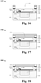
- Figs. 10-29 illustrate cross-sectional views 1000-2900 of some embodiments of a method for forming a BSI image sensor including a pixel isolation structure, the pixel isolation structure comprising a dummy contact structure 123.
- Figs. 10-29 are described in relation to a method, it will be appreciated that the structures disclosed in Figs. 10-29 are not limited to such a method, but instead may stand alone as structures independent of the method.
- a photodetector 105 may be formed in a front side 102fs of a substrate 102.
- the photodetector 105 may comprise a first doped semiconductor region 108.
- a doping type of the first doped semiconductor region 108 may be opposite a doping type of the substrate 102 such that together, the two from a p-n junction (i.e., a photodiode).
- a floating diffusion (FD) region 106 may also be formed in the front side 102fs of the substrate 102.
- a pixel transistor 104 may be formed along the front side 102fs of the substrate 102.
- the first doped semiconductor region 108 and the FD region 106 may be formed in the substrate 102 by ion implantation or another suitable process.
- a first etch stop layer 112 and a first dielectric layer 114 may be formed on the front side of the substrate such that the first etch stop layer 112 vertically separates the first dielectric layer 114 from the substrate 102.
- the first dielectric layer 114 may cover the pixel transistor 104.
- the first etch stop layer 112 and the first dielectric layer 114 may, for example, be formed by chemical vapor deposition (CVD), physical vapor deposition (PVD), atomic layer deposition (ALD), a spin-on process, another suitable deposition process, or any combination of the foregoing.
- a first photoresist mask 116 may be formed over the first dielectric layer 114.
- the first dielectric layer 114 and the first etch stop layer 112 may be patterned with the first photoresist mask 116 in place to form a plurality of contact openings in the first dielectric layer 114 and the first etch stop layer 112.
- the plurality of contact openings may comprise a first contact opening 118 and a pair of dummy contact openings 118d.
- the pair of dummy contact openings 118d may uncover a portion of the front side 102fs of the substrate 102.
- the patterning may, for example, comprise a wet etch, a dry etch, or some other suitable etch.
- the first contact opening 118 may be formed over the FD region 106.
- the pair of dummy contact openings 118d may, for example, be formed on opposing sides of the photodetector 105.
- the dummy contact openings 118d correspond to segments of a ring-shaped opening having the same layout as the dummy contact structure in Fig. 2 .
- Other suitable top layouts are, however, amenable.
- the plurality of contact openings may extend through the first dielectric layer 114 and the first etch stop layer 112 to the front side 102fs of the substrate 102.
- a first contact 122 and a dummy contact structure 123 comprising a first dummy segment 123a and a second dummy segment 123b may be formed in the first contact opening 118 and the pair of dummy contact openings 118d, respectively, by depositing a first metal material in the aforementioned openings.
- the first metal material may overlie a top of the first dielectric layer 114 after it is deposited.
- Depositing the first metal material may, for example, comprise a sputtering process, an electroplating process, another suitable deposition process, or any combination of the foregoing.
- a planarization process may be performed to remove the first metal material from the top of the first dielectric layer 114 such that tops of the first contact 122, the first dummy segment 123a, and the second dummy segment 123b are even with a top of the first dielectric layer 114.
- the first and second dummy segments 123a, 123b correspond to segments of a ring-shaped dummy contact structure having the same layout as the dummy contact structure in Fig. 2 .
- the planarization process may, for example, comprise a chemical mechanical polish (CMP) or some other suitable planarization process.
- a second etch stop layer 124 and a second dielectric layer 126 may be formed over the first dielectric layer 114 and over the tops of the first contact 122, the first dummy segment 123a, and the second dummy segment 123b.
- the second etch stop layer 124 and the second dielectric layer 126 may, for example, be formed by CVD, PVD, ALD, a spin-on process, another suitable deposition process, or any combination of the foregoing.
- a second photoresist mask 128 may be formed over the second dielectric layer 126.
- the second dielectric layer 126 and the second etch stop layer 124 may be patterned with the second photoresist mask 128 in place to form a first trench opening 130 in the second dielectric layer 126 and the second etch stop layer 124.
- the first trench opening 130 may extend over the photodetector 105 and may further extend from over a top of the first dummy segment 123a to over a top of the second dummy segment 123b (i.e., between the first dummy segment 123a and the second dummy segment 123b).
- the patterning may, for example, comprise a wet etch, a dry etch, or some other suitable etch.
- a first metal line 132 may be formed in the first trench opening 130 by depositing a second metal material in the first trench opening 130.
- the second metal material may overlie a top the second dielectric layer 126 after it is deposited and may continuously extend from over a top of the first dummy segment 123a to over a top of the second dummy segment 123b.
- Depositing the second metal material may, for example, comprise a sputtering process, an electroplating process, another suitable deposition process, or any combination of the foregoing.
- a planarization process may be performed to remove the second metal material from the top of the second dielectric layer 126 such that top of the first metal line 132 may be even with a top of the second dielectric layer 126.
- the polishing or planarization process may, for example, comprise a CMP or some other suitable planarization process.
- one or more dielectric layers and a one or more etch stop layers may be formed over the first metal line 132.
- a third etch stop layer 134 may be formed over the first metal line 132 and the second dielectric layer 126
- a third dielectric layer 136 may be formed over the third etch stop layer 134
- a fourth etch stop layer 135 may be formed over the third dielectric layer 136
- a fourth dielectric layer 137 may be formed over the fourth etch stop layer 135.
- Any of the aforementioned layers may, for example, be formed by CVD, PVD, ALD, a spin-on process, another suitable deposition process, or any combination of the foregoing.
- one or more metal lines and one or more vias may be formed over the first metal line 132.
- a first via 138 may be formed within the third dielectric layer 136 and over the first metal line 132.
- the first via 138 may directly contact the first metal line.
- a second metal line 140 may be formed in the fourth dielectric layer 137 and over the first via 138.
- the second metal line 140 may directly contact the first via.
- Any of the aforementioned metal lines and vias may, for example, be formed by sputtering, an electroplating process, another suitable deposition process, or any combination of the foregoing.
- additional interconnects 142 may be formed over the second metal line 140.
- the additional interconnects 142 may comprise additional metal lines and additional vias.
- the additional interconnects 142 may, for example, be formed by sputtering, an electroplating process, another suitable deposition process, or any combination of the foregoing.
- the image sensor may be rotated such that a back side 102bs of the substrate 102 overlies the front side 102fs of the substrate 102.
- a third photoresist mask 144 may be formed over the back side 102bs of the substrate 102.
- the back side 102bs of the substrate 102 may be patterned with the third photoresist mask 144 in place to form a pair of isolation openings 146 in the back side 102bs of the substrate 102.
- the pair of isolation openings 146 may extend through the substrate from the back side 102bs to the front side 102fs on opposing sides of the photodetector 105.
- the pair of isolation openings 146 may be formed over the first dummy segment 123a and the second dummy segment 123b (i.e., the pair of isolation openings 146 may be respectively aligned with the first dummy segment 123a and the second dummy segment 123b).
- the isolation openings 146 correspond to segments of a ring-shaped opening having the same layout as the substrate isolation structure in Fig. 2 .
- Other suitable layouts are, however, amenable.
- the patterning may, for example, comprise a wet etch, a dry etch, or some other suitable etch.
- a substrate isolation structure 150 may be formed over the back side 102bs of the substrate 102 and may be formed in the pair of isolation openings 146 to define a first isolation segment 150a and a second isolation segment 150b.
- the substrate isolation structure 150 is ring shaped as in Fig. 2 and the first and second isolation segments 150a, 150b correspond to segments of the ring shape.
- Other suitable layouts are, however, amenable.
- the substrate isolation structure 150 may be formed by depositing a first isolation material over the back side 102bs of the substrate 102 and in the pair of isolation openings 146.
- Deposing the first isolation material may, for example, comprise CVD, PVD, ALD, a spin-on process, another suitable deposition process, or any combination of the foregoing.
- forming the substrate isolation structure 150 may further comprise depositing a second isolation material over the first isolation material such that the substrate isolation structure 150 comprises a first isolation layer 145 and a second isolation layer 147 surrounded by the first isolation layer 145, as seen in Fig. 5 .
- a planarization process may be performed to reduce a thickness of the substrate isolation structure 150.
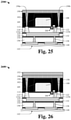
- the substrate isolation structure 150 may extend over the photodetector 105 after the planarization process (i.e., the substrate isolation structure 150 may cover the back side 102bs of the substrate 102 after the planarization process), as illustrated in Fig. 25 .
- the substrate isolation structure 150 may not extend over the photodetector 105 after the polishing or planarization process (i.e., the substrate isolation structure 150 may not cover the back side 102bs of the substrate 102 after the polishing or planarization process).
- the planarization process may, for example, comprise a CMP or some other suitable planarization process.
- a buffer layer 152 may be formed over the back side 102bs of the substrate 102 and over a top of the substrate isolation structure 150.
- the buffer layer 152 may, for example, be formed by CVD, PVD, ALD, a spin-on process, another suitable deposition process, or any combination of the foregoing.
- a metal grid layer 154 may be formed over the buffer layer 152 and a dielectric grid layer 156 may be formed over the metal grid layer 154.
- the metal grid layer 154 may, for example, be formed by depositing a metal material over the buffer layer 152 with a sputtering process, an electroplating process, another suitable deposition process, or any combination of the foregoing.
- the dielectric grid layer 156 may, for example, be formed over the metal grid layer 154 by CVD, PVD, ALD, a spin-on process, another suitable deposition process, or any combination of the foregoing.
- a fourth photoresist mask 158 may be formed over the dielectric grid layer 156.
- the dielectric grid layer 156 and the metal grid layer 154 may be patterned with the fourth photoresist mask 158 in place to form a CMG 155 over the back side 102bs of the substrate 102.
- the CMG may be formed directly over the first isolation segment 150a and the second isolation segment 150b.
- the patterning may, for example, comprise a wet etch, a dry etch, or some other suitable etch.
- one or more color filters may be formed over the over the buffer layer 152 and laterally adjacent to the CMG 155.
- one or more micro-lenses may be formed over the one or more color filters, respectively.
- a color filter 160 may be formed over the buffer layer 152 and between the CMG 155 and a micro-lens 162 may be formed directly over the color filter.
- a first region of the first dielectric layer 114 may be isolated from neighboring regions of the first dielectric layer 114 corresponding to neighboring pixels. Further, by forming the substrate isolation structure 150 directly over the dummy contact structure 123, a first region of the substrate 102 may also be isolated from neighboring regions of the substrate 102 corresponding to neighboring pixels. Furthermore, by forming the first metal such that the first metal line extends continuously between the first dummy segment 123a and the second dummy segment, the pixel 111 may be further isolated from neighboring pixels at the interconnect level. Thus, the likelihood of a photon exiting the pixel 111 and entering a neighboring pixel at the first dielectric layer 114 and/or at the substrate 102 may be reduced. As a result, the performance of the image sensor may be increased.
- Fig. 30 illustrates a flow diagram of some embodiments of a method 3000 for forming a BSI image sensor including a pixel isolation structure, the pixel isolation structure comprising a dummy contact structure.
- method 3000 is illustrated and described below as a series of acts or events, it will be appreciated that the illustrated ordering of such acts or events are not to be interpreted in a limiting sense. For example, some acts may occur in different orders and/or concurrently with other acts or events apart from those illustrated and/or described herein. In addition, not all illustrated acts may be required to implement one or more aspects or embodiments of the description herein. Further, one or more of the acts depicted herein may be carried out in one or more separate acts and/or phases.
- a photodetector may be formed in a front side of a substrate and a first dielectric layer may be formed on the front side of the substrate.
- Figs. 10 and 11 illustrate cross-sectional views 1000 and 1100 of some embodiments corresponding to act 3002.
- the first dielectric layer may then be patterned to form a dummy contact opening in the first dielectric layer and on opposite sides of the photodetector.
- Fig. 12 illustrates a cross-sectional view 1200 of some embodiments corresponding to act 3004.
- a first metal material may be deposited in the dummy contact opening to form a dummy contact structure in the of dummy contact opening.
- Fig. 13 illustrates a cross-sectional view 1300 of some embodiments corresponding to act 3006.
- a second dielectric layer may be formed over the first dielectric layer and over the top of the dummy contact structure.
- Fig. 15 illustrates a cross-sectional view 1500 of some embodiments corresponding to act 3008.
- the second dielectric layer may be patterned to form a first trench opening in the second dielectric layer.
- the first trench opening may extend over the photodetector and may further extend from over a top of a first dummy segment and a top of a second dummy segment of the dummy contact structure.
- Fig. 16 illustrates a cross-sectional view 1600 of some embodiments corresponding to act 3010.
- a second metal material may be deposited in the first trench opening to form a first metal line in the first trench opening.
- Fig. 17 illustrates a cross-sectional view 1700 of some embodiments corresponding to act 3012.
- one or more dielectric layers, one or more metal lines, and one or more vias may be formed over the first metal line.
- Figs. 19 and 20 illustrate cross-sectional views 1900 and 2000 of some embodiments corresponding to act 3014.
- the substrate may be rotated such that a back side of the substrate overlies the front side of the substrate.
- Fig. 22 illustrates a cross-sectional view 2200 of some embodiments corresponding to act 3016.
- the back side of the substrate may be patterned to form an isolation opening in back side of the substrate.
- the isolation opening may extend through the substrate from the back side to the front side on opposing sides of the photodetector. Further, the isolation opening may be formed over the first dummy segment and the second dummy segment.
- Fig. 23 illustrates a cross-sectional view 2300 of some embodiments corresponding to act 3018.
- a first isolation material may be deposited over the back side of the substrate and in the isolation opening to form a substrate isolation structure.
- Fig. 24 illustrates a cross-sectional view 2400 of some embodiments corresponding to act 3020.
- a planarization process may be performed on the first isolation material.
- Fig. 25 illustrates a cross-sectional view 2500 of some embodiments corresponding to act 3022.
- a buffer layer may be formed over the back side of the substrate and over a top of the substrate isolation structure.
- Fig. 26 illustrates a cross-sectional view 2600 of some embodiments corresponding to act 3024.
- a composite metal grid may be formed over the back side of the substrate.
- Figs. 27 and 28 illustrate cross-sectional views 2700 and 2800 of some embodiments corresponding to act 3026.
- one or more color filters may be formed over the over the buffer layer and laterally adjacent to the CMG.
- one or more micro-lenses may be formed over the one or more color filters, respectively.
- Fig. 29 illustrates a cross-sectional view 2900 of some embodiments corresponding to act 3028.
- Figs. 31-44 illustrate cross-sectional views 3100-4400 of some embodiments of a method for forming an FSI image sensor including a pixel isolation structure, the pixel isolation structure comprising a dummy contact structure 123.
- Figs. 31-44 are described in relation to a method, it will be appreciated that the structures disclosed in Figs. 31-44 are not limited to such a method, but instead may stand alone as structures independent of the method.
- Figs. 31-40 illustrate a similar process as that which is illustrated in Figs. 10-25 .
- metal lines may be restricted to sides of the photodetector 105 so as not to block the photodetector 105 from receiving radiation from the front side 102fs of the substrate 102.
- one or more metal lines e.g., 133, 140, etc.
- a first metal line 133 may not extend from a top of the first dummy segment 123a to a top of the second dummy segment 123b, as seen in Fig. 36 .
- the image sensor may be rotated again such that a front side 102fs of the substrate 102 overlies a back side 102bs of the substrate 102.
- a metal grid layer 154 may be formed over the front side 102fs of the substrate 102 and a dielectric grid layer 156 may be formed over the metal grid layer 154.
- the metal grid layer 154 may be formed by depositing a metal material over the buffer layer 152 by sputtering, electroplating, another suitable deposition process, or any combination of the foregoing.
- the dielectric grid layer 156 may, for example, be formed by depositing a dielectric material over the metal material by CVD, PVD, ALD, a spin-on process, another suitable deposition process, or any combination of the foregoing.
- a fourth photoresist mask 158 may be formed over the dielectric grid layer 156.
- the dielectric grid layer 156 and the metal grid layer 154 may be patterned with the fourth photoresist mask 158 in place to form a CMG 155 over the front side 102fs of the substrate 102.
- the patterning may, for example, comprise a wet etch, a dry etch, or some other suitable etch.
- one or more color filters may be formed over the over the front side 102fs of the substrate 102 and adjacent to the CMG 155.
- one or more micro-lenses may be formed over the one or more color filters, respectively.
- a color filter 160 may be formed over the front side 102fs of the substrate 102 and between the CMG 155 and a micro-lens 162 may be formed directly over the color filter.
- the pixel 111 may be isolated from neighboring pixels.
- the likelihood of a photon exiting the pixel 111 and entering a neighboring pixel at the first dielectric layer 114 and/or at the substrate 102 may be reduced.
- the performance of the image sensor may be increased.
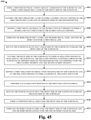
- Fig. 45 illustrates a flow diagram of some embodiments of a method 4500 for forming an FSI image sensor including a pixel isolation structure, the pixel isolation structure comprising a dummy contact structure.
- method 4500 is illustrated and described below as a series of acts or events, it will be appreciated that the illustrated ordering of such acts or events are not to be interpreted in a limiting sense. For example, some acts may occur in different orders and/or concurrently with other acts or events apart from those illustrated and/or described herein. In addition, not all illustrated acts may be required to implement one or more aspects or embodiments of the description herein. Further, one or more of the acts depicted herein may be carried out in one or more separate acts and/or phases.
- a photodetector may be formed in a front side of a substrate and a first dielectric layer may be formed on the front side of the substrate.
- Figs. 31 and 32 illustrate cross-sectional views 3100 and 3200 of some embodiments corresponding to act 4502.
- the first dielectric layer may then be patterned to form a dummy contact opening in the first dielectric layer and on opposite sides of the photodetector.
- Fig. 33 illustrates a cross-sectional view 3300 of some embodiments corresponding to act 4504.
- a first metal material may be deposited in the dummy contact opening to form a dummy contact structure in the dummy contact opening.
- Fig. 34 illustrates a cross-sectional view 3400 of some embodiments corresponding to act 4506.
- Fig. 36 illustrates a cross-sectional view 3600 of some embodiments corresponding to act 4508.
- the substrate may be rotated such that a back side of the substrate overlies the front side of the substrate.
- Fig. 37 illustrates a cross-sectional view 3700 of some embodiments corresponding to act 4510.
- the back side of the substrate may be patterned to form an isolation opening in back side of the substrate.
- the isolation opening may extend through the substrate from the back side to the front side on opposing sides of the photodetector. Further, the isolation opening may be formed over the first dummy segment and the second dummy segment.
- Fig. 38 illustrates a cross-sectional view 3800 of some embodiments corresponding to act 4512.
- a first isolation material may be deposited over the back side of the substrate and in the isolation opening to form a substrate isolation structure.
- Fig. 39 illustrates a cross-sectional view 3900 of some embodiments corresponding to act 4514.
- a planarization process may be performed on the first isolation material.
- Fig. 40 illustrates a cross-sectional view 4000 of some embodiments corresponding to act 4516.
- the substrate may be rotated again such that the front side of the substrate overlies the back side of the substrate.
- Fig. 41 illustrates a cross-sectional view 4100 of some embodiments corresponding to act 4518.
- a composite metal grid may be formed over the front side of the substrate.
- Figs. 42 and 43 illustrate cross-sectional views 4200 and 4300 of some embodiments corresponding to act 4520.
- one or more color filters may be formed over the over the front side of the substrate and laterally adjacent to the CMG.
- one or more micro-lenses may be formed over the one or more color filters, respectively.
- Fig. 44 illustrates a cross-sectional view 4400 of some embodiments corresponding to act 4522.
- the present disclosure relates to an image sensor including a pixel isolation structure, the pixel isolation structure comprising a dummy contact structure for improving pixel isolation to reduce crosstalk between pixels, and a method for forming the image sensor.
- the present disclosure relates to an image sensor structure.
- the image sensor structure comprises a substrate.
- the substrate comprises a first side and a second side opposite the first side.
- a photodetector extends into the first side of the substrate.
- An isolation structure comprises a first isolation segment and a second isolation segment that extend through the substrate. The first isolation segment and the second isolation segment are respectively on opposite sides of the photodetector and comprise a dielectric.
- a first metal line is on the first side of the substrate.
- a dummy contact structure comprises a first dummy segment and a second dummy segment. Both the first dummy segment and the second dummy segment comprise metal and extend from the first metal line to the first isolation segment and the second isolation segment, respectively.
- the present disclosure relates to an image sensor structure.
- the image sensor structure comprises a substrate.
- the substrate comprises an upper surface and a lower surface.
- a pixel comprises a photodetector along the lower surface of the substrate.
- a substrate isolation structure comprises a first dielectric material.
- the substrate isolation structure extends vertically through the substrate from the upper surface of the substrate to the lower surface of the substrate.
- the substrate isolation structure extends laterally along a boundary of the pixel in a first closed path.
- a metal reflector underlies the photodetector.
- a dummy contact structure comprising a first metal material extends from the metal reflector to the substrate isolation structure. The dummy contact structure also extends laterally along the boundary of the pixel in the first closed path.
- the present disclosure relates to a method for forming an image sensor structure.
- the method comprises forming a photodetector in a first side of a substrate and forming a first dielectric layer on the first side of the substrate.
- the first dielectric layer is patterned to form a first opening having a pair of first opening segments that uncover the first side of the substrate.
- the first opening segments border the photodetector respectively on opposite sides of the photodetector.
- a dummy contact structure is formed in the first opening and comprises a first dummy segment and a second dummy segment respectively in the first opening segments.
- a metal reflector is formed directly contacting the first dummy segment and the second dummy segment on the first side of the substrate.
- a second side of the substrate opposite the first side is patterned to form a second opening having a pair of second opening segments that are aligned to the first dummy segment and the second dummy segment, respectively.
- a substrate isolation structure is formed in the second opening and comprises a first isolation segment and a second isolation segment respectively in the second opening segments.
Landscapes
- Solid State Image Pick-Up Elements (AREA)
- Element Separation (AREA)
Abstract
Description
- Integrated circuits (ICs) with image sensors are used in a wide range of modern day electronic devices, such as, for example, cameras and cell phones. In recent years, complementary metal-oxide-semiconductor (CMOS) image sensors have begun to see widespread use, largely replacing charge-coupled device (CCD) image sensors. Compared to CCD image sensors, CMOS image sensors are favored due to low power consumption, small size, fast data processing, a direct output of data, and low manufacturing cost. Some types of CMOS image sensors include front-side illuminated (FSI) image sensors and back-side illuminated (BSI) image sensors.
- Aspects of the present disclosure are best understood from the following detailed description when read with the accompanying figures. It is noted that, in accordance with the standard practice in the industry, various features are not drawn to scale. In fact, the dimensions of the various features may be arbitrarily increased or reduced for clarity of discussion.
-
Fig. 1 illustrates a cross-sectional view of some embodiments of an image sensor including a pixel isolation structure, the pixel isolation structure comprising a dummy contact structure. -
Fig. 2 illustrates an overhead view of some embodiments of the image sensor ofFig. 1 . -
Figs. 3-5 illustrate cross-sectional views of some additional embodiments of an image sensor including a pixel isolation structure, the pixel isolation structure comprising a dummy contact structure. -
Fig. 6 illustrates a cross-sectional view of some embodiments of a back-side illuminated (BSI) image sensor including a pixel isolation structure, the pixel isolation structure comprising a dummy contact structure. -
Fig. 7 illustrates a cross-sectional view of some embodiments of a front-side illuminated (FSI) image sensor including a pixel isolation structure, the pixel isolation structure comprising a dummy contact structure. -
Fig. 8 illustrates a cross-sectional view of some additional embodiments of an image sensor comprising a plurality of pixels and a pixel isolation structure, the pixel isolation structure comprising a dummy contact structure. -
Fig. 9 illustrates an overhead view of some embodiments of the image sensor ofFig. 8 . -
Figs. 10-29 illustrate a series of cross-sectional views of some embodiments of a method for forming a BSI image sensor including a pixel isolation structure, the pixel isolation structure comprising a dummy contact structure. -
Fig. 30 illustrates a flow diagram of some embodiments of a method for forming a BSI image sensor including a pixel isolation structure, the pixel isolation structure comprising a dummy contact structure. -
Figs. 31-44 illustrate a series of cross-sectional views of some embodiments of a method for forming FSI an image sensor including a pixel isolation structure, the pixel isolation structure comprising a dummy contact structure. -
Fig. 45 illustrates a flow diagram of some embodiments of a method for forming an FSI image sensor including a pixel isolation structure, the pixel isolation structure comprising a dummy contact structure. - The following disclosure provides many different embodiments, or examples, for implementing different features of the provided subject matter. Specific examples of components and arrangements are described below to simplify the present disclosure. These are, of course, merely examples and are not intended to be limiting. For example, the formation of a first feature over or on a second feature in the description that follows may include embodiments in which the first and second features are formed in direct contact, and may also include embodiments in which additional features may be formed between the first and second features, such that the first and second features may not be in direct contact. In addition, the present disclosure may repeat reference numerals and/or letters in the various examples. This repetition is for the purpose of simplicity and clarity and does not in itself dictate a relationship between the various embodiments and/or configurations discussed.
- Further, spatially relative terms, such as "beneath," "below," "lower," "above," "upper" and the like, may be used herein for ease of description to describe one element or feature's relationship to another element(s) or feature(s) as illustrated in the figures. The spatially relative terms are intended to encompass different orientations of the device in use or operation in addition to the orientation depicted in the figures. The apparatus may be otherwise oriented (rotated 90 degrees or at other orientations) and the spatially relative descriptors used herein may likewise be interpreted accordingly.
- Many modern integrated chips comprise image sensors. An image sensor may include a semiconductor substrate and a metal interconnect structure disposed on a front side of the substrate. Further, the image sensor may include a plurality of pixels. Each pixel includes a photodetector in the semiconductor substrate. Further, the pixels are separated from each other by a shallow trench isolation (STI) structure disposed in the front side of the substrate and a deep trench isolation (DTI) structure disposed in a back side of substrate opposite the front side. The DTI structure and the STI structure may be arranged along a common vertical axis. Further, the DTI structure and the STI structure may together extend vertically through the substrate at boundaries of the pixels to separate the pixels. As a result, photons entering a portion of a substrate corresponding to a pixel may be confined to the portion and prevented from entering other portions of the substrate corresponding to neighboring pixels.
- A challenge with the image sensor is that while the DTI and STI structures may separate the pixels at the substrate, the DTI and STI structure do not separate the pixels at the interconnect structure. For example, a first dielectric layer of the interconnect structure that is disposed along the substrate may not be isolated at the boundaries between the pixels. As a result, some photons may travel between neighboring pixels via the non-isolated first dielectric layer. Thus, the STI and DTI structures intended to isolate neighboring pixels from one another may not prevent some photons from traveling between the neighboring pixels. This may, in turn, lead to high crosstalk between pixels and may decrease performance (e.g., quantum efficiency (QE)) of the image sensor.
- Various embodiments of the present disclosure are directed towards an image sensor including a pixel isolation structure, the pixel isolation structure comprising a dummy contact structure for improving pixel isolation and reducing crosstalk between pixels. The image sensor may comprise a semiconductor substrate and a plurality of pixels along the substrate. A pixel of the plurality of pixels may comprise a photodetector in the substrate. The pixel isolation structure may include a substrate isolation structure disposed in the substrate and a dummy contact structure disposed in a first dielectric layer that together extend vertically through the substrate and through the first dielectric layer along a boundary of the pixel to separate a first region of the substrate and a first region of the first dielectric layer that are associated with the pixel from neighboring regions of the substrate and neighboring regions of the first dielectric layer that are associated with neighboring pixels. Thus, pixel isolation from neighboring pixels may be improved. As a result, the pixel isolation structure may reduce the likelihood that photons which enter the pixel will exit the pixel and enter a neighboring pixel. In turn, less cross talk may occur between neighboring pixels, thereby improving performance (e.g., QE) of the image sensor.
-
Fig. 1 illustrates across-sectional view 100 of some embodiments of an image sensor including apixel isolation structure 120, thepixel isolation structure 120 comprising adummy contact structure 123. Thecross-sectional view 100 may, for example, be taken across the line A-A' illustrated inFig. 2 . - The image sensor comprises a
pixel 111. The image sensor further comprises asubstrate 102, aphotodetector 105 in thesubstrate 102, a firstetch stop layer 112 along a lower surface of thesubstrate 102, a firstdielectric layer 114 along a lower surface of the firstetch stop layer 112, a secondetch stop layer 124 along a lower surface of the firstdielectric layer 114, a seconddielectric layer 126 along a lower surface of the secondetch stop layer 124, and afirst metal line 132 disposed within the seconddielectric layer 126. In some embodiments, thefirst metal line 132 may be used as a metal reflector. In some embodiments, the image sensor may further comprise an interconnect structure (not labeled) below thesubstrate 102. For example, the interconnect structure may include the firstdielectric layer 114, thedummy contact structure 123, and/or thefirst metal line 132, and may further include a number of other metal lines or vias (not shown). - The
pixel isolation structure 120 comprises asubstrate isolation structure 150 and thedummy contact structure 123. Thesubstrate isolation structure 150 comprises afirst isolation segment 150a and asecond isolation segment 150b that extend vertically through the substrate along a boundary of thepixel 111. As a result, thefirst isolation segment 150a and thesecond isolation segment 150b laterally separate a first region of thesubstrate 102a from neighboring regions of thesubstrate 102n (and thus separate thephotodetector 105 from neighboring photodetectors (not shown) that are in the neighboring regions of thesubstrate 102n). Moreover, sidewalls of thefirst isolation segment 150a and thesecond isolation segment 150b define the first region of thesubstrate 102a that comprises thephotodetector 105. Further, thesubstrate isolation structure 150 may be a grid structure or a ring-like structure, as shown inFig. 2 . Furthermore, thesubstrate isolation structure 150 vertically extends from a top surface that is over thesubstrate 102 to a bottom surface that is below a top of thesubstrate 102. For example, thesubstrate isolation structure 150 comprises afront cover 150f that extends over a top surface of thesubstrate 102 between thefirst isolation segment 150a and thesecond isolation segment 150b. Aphoton 170 may enter thesubstrate 102 through thefront cover 150f. - The
dummy contact structure 123 comprises afirst dummy segment 123a and asecond dummy segment 123b that extend from thefirst metal line 132 to thefirst isolation segment 150a and thesecond isolation segment 150b, respectively. As a result, thefirst dummy segment 123a and thesecond dummy segment 123b laterally separate a first region of thefirst dielectric layer 114a from neighboring regions of thefirst dielectric layer 114n. In some embodiments, thepixel isolation structure 120 and thefirst metal line 132 completely enclose the first region of thesubstrate 102a and the first region of thefirst dielectric layer 114a. - The
pixel isolation structure 120 may reduce the likelihood that aphoton 170 which enters thepixel 111 will exit thepixel 111 and enter a neighboring pixel. Thesubstrate isolation structure 150 reduces the likelihood of thephoton 170 entering the neighboring pixel at thesubstrate 102. Further, thedummy contact structure 123 reduces the likelihood of thephoton 170 entering the neighboring pixel at thefirst dielectric layer 114. Moreover, thedummy contact structure 123 together with thefirst metal line 132 may isolate the pixel at the interconnect structure (not labeled), thereby reducing the likelihood of thephoton 170 entering the neighboring pixel at the interconnect structure. Thus, thepixel isolation structure 120 may improve an isolation of thepixel 111 from neighboring pixels. In turn, less cross talk may occur between thepixel 111 and neighboring pixels, thereby improving a QE and other performance metrics of image sensor. - In some embodiments, the
substrate isolation structure 150 comprises one or more isolation materials. The one or more isolation materials may, for example, comprise silicon dioxide, silicon nitride, a low k dielectric, hafnium oxide, aluminum oxide, a high k dielectric, tungsten, aluminum, another suitable material, or any combination of the foregoing. In some embodiments, thesubstrate isolation structure 150 has a refractive index less than that of thesubstrate 102 to provide optical isolation via total internal reflection. - In some embodiments, the
first isolation segment 150a, thesecond isolation segment 150b, and thefront cover 150f may be integrally formed with same material, such as an oxide (e.g., silicon oxide), tetraethyl orthosilicate (TEOS), or the like. Further, an anti-reflective layer (not shown) may be disposed over thesubstrate 102 between thesubstrate 102 and thefront cover 150f. The anti-reflective layer may also be disposed along sidewalls of thefirst isolation segment 150a and sidewalls of thesecond isolation segment 150b such that the anti-reflective layer is between thefirst isolation segment 150a and thesubstrate 102 and also between thesecond isolation segment 150b and thesubstrate 102. In some embodiments, thefront cover 150f may have curved surfaces arranged over thephotodetector 105 and intersecting one another. - In some other embodiments, the
first isolation segment 150a and thesecond isolation segment 150b may be formed with different materials than thefront cover 150f. For example, a reflective material may be disposed within thefirst isolation segment 150a and thesecond isolation segment 150b, such as aluminum (Al), rhodium (Rh), ruthenium (Ru), copper (Cu), silver (Ag), gold (Au), tungsten (W), cobalt (Co), iron (Fe), molybdenum (Mo), titanium (Ti), chromium (Cr), or any combination of the foregoing. - In some embodiments, the
dummy contact structure 123 comprises a first metal material. The first metal material may, for example, comprise tungsten, copper, titanium, another suitable metal, or any combination of the foregoing. Thedummy contact structure 123 may have a greater width than thesubstrate isolation structure 150 at an interface between thedummy contact structure 123 and the substrate isolation structure 150 (i.e. along a top surface of the dummy contact structure 123). Further, thedummy contact structure 123 may have a height that is less than that of thesubstrate isolation structure 150. Furthermore, thedummy contact structure 123 may have some other surface geometries (e.g., multifaceted or bulbous in shape). - In some embodiment's, the image sensor is a CMOS image sensor or the like. In some embodiments, the
substrate 102 may, for example, comprise a semiconductor material such as silicon or the like. - In some embodiments, the
first dielectric layer 114 and thesecond dielectric layer 126 may, for example, comprise silicon dioxide, silicon nitride, a low k dielectric, another suitable dielectric material, or any combination of the foregoing. In addition, the firstetch stop layer 112 and the secondetch stop layer 124 may, for example, comprise silicon nitride, silicon carbide, silicon carbonitride, another suitable dielectric, or any combination of the foregoing. - In some embodiments, the
first metal line 132 comprises a second metal material. The second metal material may, for example, comprise copper, aluminum copper, tungsten, another suitable metal, or any combination of the foregoing. -
Fig. 2 illustrates anoverhead view 200 of some embodiments of the image sensor ofFig. 1 . A portion of thesubstrate isolation structure 150 in thesubstrate 102 may have a ring-shaped top layout. The ring-shaped portion of thesubstrate isolation structure 150 may extend along the boundary of thepixel 111 in a first closed path. Thedummy contact structure 123 may be disposed directly below the ring-shaped portion of thesubstrate isolation structure 150 and may have the same top layout as the ring-shaped portion (i.e., thedummy contact structure 123 may be ring-shaped, may extend along the boundary of thepixel 111, and may extend along the first closed path). - In some embodiments, the
first metal line 132, thedummy contact structure 123, and thesubstrate isolation structure 150 define a composite structure (not labeled) that extends vertically in a second closed path around the photodetector 105 (see, for example,Fig. 1 ). -
Fig. 3 illustrates across-sectional view 300 of some additional embodiments of an image sensor in which thesubstrate isolation structure 150 does not extend over and along a top of thesubstrate 102 between thefirst isolation segment 150a and thesecond isolation segment 150b. Instead, a top surface of thesubstrate isolation structure 150 is even with or about even with a top surface of thesubstrate 102. -
Fig. 4 illustrates across-sectional view 400 of some additional embodiments an image sensor in whichsubstrate isolation structure 150 is divided into a DTI structure and an STI structure. Thefirst isolation segment 150a and thesecond isolation segment 150b comprise afirst DTI segment 151a and asecond DTI segment 151b, respectively, that extend into an upper side of thesubstrate 102 to afirst depth 148 and that define the DTI structure. Further, thefirst isolation segment 150a and thesecond isolation segment 150b comprise afirst STI segment 153a and asecond STI segment 153b, respectively, that extend into a lower side of thesubstrate 102 to asecond depth 149 less than thefirst depth 148 and that define the STI structure. - The
first STI segment 153a and thesecond STI segment 153b may be disposed directly below thefirst DTI segment 151a and thesecond DTI segment 151b, respectively. In addition, thefirst dummy segment 123a and thesecond dummy segment 123b may be disposed directly below thefirst STI segment 153a and thesecond STI segment 153b, respectively, such that thefirst DTI segment 151a, thefirst STI segment 153a, and thefirst dummy segment 123a are disposed along a first commonvertical axis 164a and thesecond DTI segment 151b, thesecond STI segment 153b, and thesecond dummy segment 123b are disposed along a second commonvertical axis 164b. Thus, thefirst STI segment 153a and thesecond STI segment 153b may vertically separate thefirst DTI segment 151a from thefirst dummy segment 123a and thesecond DTI segment 151b from thesecond dummy segment 123b, respectively. Further, thefirst DTI segment 151a may directly contact thefirst STI segment 153a and thefirst STI segment 153a may directly contact thefirst dummy segment 123a. In addition, thesecond DTI segment 151b may directly contact thesecond STI segment 153b and thesecond STI segment 153b may directly contact thesecond dummy segment 123b. In some embodiments, any of the DTI segments and the STI segments may, for example, comprise the one or more isolation materials. -
Fig. 5 illustrates across-sectional view 500 of some additional embodiments an image sensor in which thefirst isolation segment 150a and thesecond isolation segment 150b are defined by afirst isolation layer 145 and asecond isolation layer 147 that comprise different materials. For example, thefirst isolation layer 145 may be or comprise a dielectric andsecond isolation layer 147 may be or comprise a metal. Thefirst isolation layer 145 may be disposed along outer sidewalls and a lower surface of thesecond isolation layer 147 such that the first isolation layers 145 surrounds thesecond isolation layer 147 and laterally separates thesecond isolation layer 147 from thesubstrate 102. - In some embodiments, the
first isolation layer 145 may, for example, comprise hafnium oxide, aluminum oxide, a high k dielectric, another suitable dielectric material, or any combination of the foregoing. In addition, thesecond isolation layer 147 may, for example, comprise silicon dioxide, silicon nitride, tungsten, another suitable material, or any combination of the foregoing. -
Fig. 6 illustrates across-sectional view 600 of some embodiments of a back-side illuminated (BSI) image sensor comprising a pixel isolation structure. The BSI image sensor comprises aphotodetector 105 in asubstrate 102 along a front side 102fs of thesubstrate 102. The photodetector may comprise a first dopedsemiconductor region 108 and a surrounding region of thesubstrate 102. The first dopedsemiconductor region 108 may form a p-n junction with the surrounding region of thesubstrate 102. - Further, a
pixel transistor 104 comprising agate 110 may be disposed along the front side 102fs of thesubstrate 102 and a floating diffusion (FD)region 106 may be disposed in thesubstrate 102 along the front side 102fs of the substrate. Afirst contact 122 may extend through a firstdielectric layer 114 to afirst metal line 132 and may electrically couple thepixel transistor 104 and/or theFD region 106 to thefirst metal line 132 or some other suitable metal line. Abuffer layer 152 may be disposed on a back side 102bs of the substrate and may extend over thephotodetector 105. - In addition, a
color filter 160 may be disposed on the back side 102bs of thesubstrate 102 and over thephotodetector 105. A composite metal grid (CMG) 155 may be disposed on the back side 102bs of thesubstrate 102 over the isolation segments (e.g., 150a, 150b) and the dummy segments (e.g., 123a, 123b) along a boundary of thepixel 111. TheCMG 155 may comprise ametal grid layer 154 and adielectric grid layer 156 over themetal grid layer 154. Thecolor filter 160 may be disposed between sidewalls of theCMG 155. A micro-lens 162 may be disposed on the back side 102bs of thesubstrate 102 over thecolor filter 160 and thus over thephotodetector 105.Photons 170 may enter the BSI image sensor through the micro-lens 162. Thus, thephotons 170 may enter thesubstrate 102 through the back side 102bs of thesubstrate 102, thereby making the image sensor "back-side illuminated". - In some embodiments, the
pixel transistor 104 may, for example, comprise a transfer transistor, a source-follower transistor, a row select transistor, a reset transistor, some other pixel transistor, or another transistor. - In some embodiments, the
FD region 106 and the first dopedsemiconductor region 108 may, for example, comprise doped silicon or the like. - In some embodiments, the
first contact 122 may, for example, comprise tungsten, copper, titanium, another suitable metal, or any combination of the foregoing. - In some embodiments, the
buffer layer 152 may, for example, comprise silicon dioxide, silicon nitride, another suitable dielectric, or any combination of the foregoing. - In some embodiments, the
metal grid layer 154 may, for example, comprise tungsten, copper, another suitable metal, or any combination of the foregoing. In some embodiments, thedielectric grid layer 156 may, for example, comprise silicon dioxide, silicon nitride, another suitable dielectric, or any combination of the foregoing. -
Fig. 7 illustrates across-sectional view 700 of some embodiments of a front-side illuminated (FSI) image sensor comprising a pixel isolation structure. The FSI image sensor comprises aphotodetector 105 in asubstrate 102 along a front side 102fs of thesubstrate 102. Afirst metal line 133 may not extend over thephotodetector 105 or past a boundary of thephotodetector 105 to allow radiation to pass to thephotodetector 105 from the front side 102fs of thesubstrate 102. One or more additional metal lines and vias (e.g., 138, 140) may be formed over thefirst metal line 133 and may not extend over thephotodetector 105 or past the boundary of thephotodetector 105. - In addition, a
color filter 160 may be disposed on the front side 102fs of thesubstrate 102 and over thephotodetector 105. ACMG 155 may be disposed on the front side 102fs of thesubstrate 102 over the isolation segments (e.g., 150a, 150b) and the dummy segments (e.g., 123a, 123b) along a boundary of thepixel 111. Thecolor filter 160 may be disposed between sidewalls of theCMG 155. A micro-lens 162 may be disposed on the front side 102fs of thesubstrate 102 over thecolor filter 160 and thus over thephotodetector 105.Photons 170 may enter the FSI image sensor through the micro-lens 162. Thus, thephotons 170 may enter thesubstrate 102 through the front side 102fs of thesubstrate 102, thereby making the image sensor "front-side illuminated". -
Fig. 8 illustrates across-sectional view 800 of some additional embodiments of an image sensor comprising a plurality of pixels and a pixel isolation structure, the pixel isolation structure comprising adummy contact structure 123. Thecross-sectional view 800 may, for example, be taken across the line B-B' illustrated inFig. 9 . Afirst pixel 111a comprising afirst photodetector 105a may be laterally adjacent to asecond pixel 111b comprising asecond photodetector 105b. Asecond isolation segment 150b may separate thesubstrate 102 along a boundary between thefirst pixel 111a and thesecond pixel 111b such that thesubstrate 102 comprises afirst substrate region 102a and a separatesecond substrate region 102b. Further, athird isolation segment 150c may be disposed along a boundary of thesecond pixel 111b. In addition, asecond dummy segment 123b may further separate thefirst pixel 111a from thesecond pixel 111b along the boundary between the pixels. Further, athird dummy segment 123c may be disposed along a boundary of thesecond pixel 111b. - Together, the
second isolation segment 150b and thesecond dummy segment 123b may isolate thefirst pixel 111a from thesecond pixel 111b. As such, afirst photon 170a that enters thefirst pixel 111a may not exit thefirst pixel 111a and enter thesecond pixel 111b. Further, asecond photon 170b that enters thesecond pixel 111b may not exit thesecond pixel 111b and enter thefirst pixel 111a. As a result, crosstalk between thefirst pixel 111a and thesecond pixel 111b may be reduced, thereby improving the performance of the image sensor. -
Fig. 9 illustrates anoverhead view 900 of some embodiments of the image sensor ofFig. 8 . The image sensor may include a pixel array comprising a plurality of pixels. For example, afirst pixel 111a, asecond pixel 111b, athird pixel 111c, and afourth pixel 111d may be disposed in a four by four array along thesubstrate 102. Asubstrate isolation structure 150 may laterally separate thefirst pixel 111a, thesecond pixel 111b, thethird pixel 111c, and thefourth pixel 111d from one another along boundaries of the aforementioned pixels (i.e., thesubstrate isolation structure 150 may continuously and individually surround thefirst pixel 111a, thesecond pixel 111b, thethird pixel 111c, and thefourth pixel 111d in a closed path along boundaries of the aforementioned pixels). As a result, thesubstrate 102 may be divided into four or more substrate regions (not shown) that are laterally separated from one another by thesubstrate isolation structure 150. Additionally, adummy contact structure 123 may be disposed directly below thesubstrate isolation structure 150. As a result, thefirst dielectric layer 114 may be divided into four or more dielectric regions (e.g., 114a, 114b, 114c, 114d) that are laterally separated from one another by thedummy contact structure 123. - In some embodiments, the
dummy contact structure 123 and thesubstrate isolation structure 150 extend laterally along a boundary of thefirst pixel 111a in a first closed path and along a boundary of thesecond pixel 111b in a second closed path. In such embodiments, the second closed path partially, but not fully, overlaps with the first closed path (e.g., between thefirst pixel 111a and thesecond pixel 111b). -
Figs. 10-29 illustrate cross-sectional views 1000-2900 of some embodiments of a method for forming a BSI image sensor including a pixel isolation structure, the pixel isolation structure comprising adummy contact structure 123. AlthoughFigs. 10-29 are described in relation to a method, it will be appreciated that the structures disclosed inFigs. 10-29 are not limited to such a method, but instead may stand alone as structures independent of the method. - As shown in
cross-sectional view 1000 ofFig. 10 , aphotodetector 105 may be formed in a front side 102fs of asubstrate 102. Thephotodetector 105 may comprise a first dopedsemiconductor region 108. A doping type of the first dopedsemiconductor region 108 may be opposite a doping type of thesubstrate 102 such that together, the two from a p-n junction (i.e., a photodiode). A floating diffusion (FD)region 106 may also be formed in the front side 102fs of thesubstrate 102. In addition, apixel transistor 104 may be formed along the front side 102fs of thesubstrate 102. In some embodiments, the first dopedsemiconductor region 108 and theFD region 106 may be formed in thesubstrate 102 by ion implantation or another suitable process. - As shown in
cross-sectional view 1100 ofFig. 11 , a firstetch stop layer 112 and a firstdielectric layer 114 may be formed on the front side of the substrate such that the firstetch stop layer 112 vertically separates thefirst dielectric layer 114 from thesubstrate 102. Thefirst dielectric layer 114 may cover thepixel transistor 104. The firstetch stop layer 112 and thefirst dielectric layer 114 may, for example, be formed by chemical vapor deposition (CVD), physical vapor deposition (PVD), atomic layer deposition (ALD), a spin-on process, another suitable deposition process, or any combination of the foregoing. - As shown in
cross-sectional view 1200 ofFig. 12 , afirst photoresist mask 116 may be formed over thefirst dielectric layer 114. Thefirst dielectric layer 114 and the firstetch stop layer 112 may be patterned with thefirst photoresist mask 116 in place to form a plurality of contact openings in thefirst dielectric layer 114 and the firstetch stop layer 112. For example, the plurality of contact openings may comprise afirst contact opening 118 and a pair ofdummy contact openings 118d. The pair ofdummy contact openings 118d may uncover a portion of the front side 102fs of thesubstrate 102. The patterning may, for example, comprise a wet etch, a dry etch, or some other suitable etch. - In some embodiments, the
first contact opening 118 may be formed over theFD region 106. In addition, the pair ofdummy contact openings 118d may, for example, be formed on opposing sides of thephotodetector 105. In some embodiments, thedummy contact openings 118d correspond to segments of a ring-shaped opening having the same layout as the dummy contact structure inFig. 2 . Other suitable top layouts are, however, amenable. The plurality of contact openings may extend through thefirst dielectric layer 114 and the firstetch stop layer 112 to the front side 102fs of thesubstrate 102. - As shown in
cross-sectional view 1300 ofFig. 13 , afirst contact 122 and adummy contact structure 123 comprising afirst dummy segment 123a and asecond dummy segment 123b may be formed in thefirst contact opening 118 and the pair ofdummy contact openings 118d, respectively, by depositing a first metal material in the aforementioned openings. The first metal material may overlie a top of thefirst dielectric layer 114 after it is deposited. Depositing the first metal material may, for example, comprise a sputtering process, an electroplating process, another suitable deposition process, or any combination of the foregoing. - As shown in
cross-sectional view 1400 ofFig. 14 , a planarization process may be performed to remove the first metal material from the top of thefirst dielectric layer 114 such that tops of thefirst contact 122, thefirst dummy segment 123a, and thesecond dummy segment 123b are even with a top of thefirst dielectric layer 114. In some embodiments, the first andsecond dummy segments Fig. 2 . The planarization process may, for example, comprise a chemical mechanical polish (CMP) or some other suitable planarization process. - As shown in
cross-sectional view 1500 ofFig. 15 , a secondetch stop layer 124 and asecond dielectric layer 126 may be formed over thefirst dielectric layer 114 and over the tops of thefirst contact 122, thefirst dummy segment 123a, and thesecond dummy segment 123b. The secondetch stop layer 124 and thesecond dielectric layer 126 may, for example, be formed by CVD, PVD, ALD, a spin-on process, another suitable deposition process, or any combination of the foregoing. - As shown in
cross-sectional view 1600 ofFig. 16 , asecond photoresist mask 128 may be formed over thesecond dielectric layer 126. Thesecond dielectric layer 126 and the secondetch stop layer 124 may be patterned with thesecond photoresist mask 128 in place to form a first trench opening 130 in thesecond dielectric layer 126 and the secondetch stop layer 124. Thefirst trench opening 130 may extend over thephotodetector 105 and may further extend from over a top of thefirst dummy segment 123a to over a top of thesecond dummy segment 123b (i.e., between thefirst dummy segment 123a and thesecond dummy segment 123b). The patterning may, for example, comprise a wet etch, a dry etch, or some other suitable etch. - As shown in
cross-sectional view 1700 ofFig. 17 , afirst metal line 132 may be formed in thefirst trench opening 130 by depositing a second metal material in thefirst trench opening 130. The second metal material may overlie a top thesecond dielectric layer 126 after it is deposited and may continuously extend from over a top of thefirst dummy segment 123a to over a top of thesecond dummy segment 123b. Depositing the second metal material may, for example, comprise a sputtering process, an electroplating process, another suitable deposition process, or any combination of the foregoing. - As shown in
cross-sectional view 1800 ofFig. 18 , a planarization process may be performed to remove the second metal material from the top of thesecond dielectric layer 126 such that top of thefirst metal line 132 may be even with a top of thesecond dielectric layer 126. The polishing or planarization process may, for example, comprise a CMP or some other suitable planarization process. - As shown in
cross-sectional view 1900 ofFig. 19 , one or more dielectric layers and a one or more etch stop layers may be formed over thefirst metal line 132. For example, a thirdetch stop layer 134 may be formed over thefirst metal line 132 and thesecond dielectric layer 126, a thirddielectric layer 136 may be formed over the thirdetch stop layer 134, a fourthetch stop layer 135 may be formed over the thirddielectric layer 136, and a fourthdielectric layer 137 may be formed over the fourthetch stop layer 135. Any of the aforementioned layers may, for example, be formed by CVD, PVD, ALD, a spin-on process, another suitable deposition process, or any combination of the foregoing. - As shown in
cross-sectional view 2000 ofFig. 20 , one or more metal lines and one or more vias may be formed over thefirst metal line 132. For example, a first via 138 may be formed within the thirddielectric layer 136 and over thefirst metal line 132. The first via 138 may directly contact the first metal line. In addition, asecond metal line 140 may be formed in thefourth dielectric layer 137 and over the first via 138. Thesecond metal line 140 may directly contact the first via. Any of the aforementioned metal lines and vias may, for example, be formed by sputtering, an electroplating process, another suitable deposition process, or any combination of the foregoing. - As shown in
cross-sectional view 2100 ofFig. 21 ,additional interconnects 142 may be formed over thesecond metal line 140. Theadditional interconnects 142 may comprise additional metal lines and additional vias. Theadditional interconnects 142 may, for example, be formed by sputtering, an electroplating process, another suitable deposition process, or any combination of the foregoing. - As shown in
cross-sectional view 2200 ofFig. 22 , the image sensor may be rotated such that a back side 102bs of thesubstrate 102 overlies the front side 102fs of thesubstrate 102. - As shown in
cross-sectional view 2300 ofFig. 23 , athird photoresist mask 144 may be formed over the back side 102bs of thesubstrate 102. The back side 102bs of thesubstrate 102 may be patterned with thethird photoresist mask 144 in place to form a pair ofisolation openings 146 in the back side 102bs of thesubstrate 102. The pair ofisolation openings 146 may extend through the substrate from the back side 102bs to the front side 102fs on opposing sides of thephotodetector 105. Further, the pair ofisolation openings 146 may be formed over thefirst dummy segment 123a and thesecond dummy segment 123b (i.e., the pair ofisolation openings 146 may be respectively aligned with thefirst dummy segment 123a and thesecond dummy segment 123b). In some embodiments, theisolation openings 146 correspond to segments of a ring-shaped opening having the same layout as the substrate isolation structure inFig. 2 . Other suitable layouts are, however, amenable. The patterning may, for example, comprise a wet etch, a dry etch, or some other suitable etch. - As shown in
cross-sectional view 2400 ofFig. 24 , asubstrate isolation structure 150 may be formed over the back side 102bs of thesubstrate 102 and may be formed in the pair ofisolation openings 146 to define afirst isolation segment 150a and asecond isolation segment 150b. In some embodiments, thesubstrate isolation structure 150 is ring shaped as inFig. 2 and the first andsecond isolation segments substrate isolation structure 150 may be formed by depositing a first isolation material over the back side 102bs of thesubstrate 102 and in the pair ofisolation openings 146. Deposing the first isolation material may, for example, comprise CVD, PVD, ALD, a spin-on process, another suitable deposition process, or any combination of the foregoing. In addition, it will be appreciated that forming thesubstrate isolation structure 150 may further comprise depositing a second isolation material over the first isolation material such that thesubstrate isolation structure 150 comprises afirst isolation layer 145 and asecond isolation layer 147 surrounded by thefirst isolation layer 145, as seen inFig. 5 . - As shown in
cross-sectional view 2500 ofFig. 25 , a planarization process may be performed to reduce a thickness of thesubstrate isolation structure 150. Thesubstrate isolation structure 150 may extend over thephotodetector 105 after the planarization process (i.e., thesubstrate isolation structure 150 may cover the back side 102bs of thesubstrate 102 after the planarization process), as illustrated inFig. 25 . However, it will be appreciated that in some alternative embodiments, thesubstrate isolation structure 150 may not extend over thephotodetector 105 after the polishing or planarization process (i.e., thesubstrate isolation structure 150 may not cover the back side 102bs of thesubstrate 102 after the polishing or planarization process). The planarization process may, for example, comprise a CMP or some other suitable planarization process. - As shown in
cross-sectional view 2600 ofFig. 26 , abuffer layer 152 may be formed over the back side 102bs of thesubstrate 102 and over a top of thesubstrate isolation structure 150. Thebuffer layer 152 may, for example, be formed by CVD, PVD, ALD, a spin-on process, another suitable deposition process, or any combination of the foregoing. - As shown in
cross-sectional view 2700 ofFig. 27 , ametal grid layer 154 may be formed over thebuffer layer 152 and adielectric grid layer 156 may be formed over themetal grid layer 154. Themetal grid layer 154 may, for example, be formed by depositing a metal material over thebuffer layer 152 with a sputtering process, an electroplating process, another suitable deposition process, or any combination of the foregoing. Thedielectric grid layer 156 may, for example, be formed over themetal grid layer 154 by CVD, PVD, ALD, a spin-on process, another suitable deposition process, or any combination of the foregoing. - As shown in
cross-sectional view 2800 ofFig. 28 , afourth photoresist mask 158 may be formed over thedielectric grid layer 156. Thedielectric grid layer 156 and themetal grid layer 154 may be patterned with thefourth photoresist mask 158 in place to form aCMG 155 over the back side 102bs of thesubstrate 102. The CMG may be formed directly over thefirst isolation segment 150a and thesecond isolation segment 150b. The patterning may, for example, comprise a wet etch, a dry etch, or some other suitable etch. - As shown in
cross-sectional view 2900 ofFig. 29 , one or more color filters may be formed over the over thebuffer layer 152 and laterally adjacent to theCMG 155. In addition, one or more micro-lenses may be formed over the one or more color filters, respectively. For example, acolor filter 160 may be formed over thebuffer layer 152 and between theCMG 155 and a micro-lens 162 may be formed directly over the color filter. - By forming the
dummy contact structure 123 in thefirst dielectric layer 114 along a boundary of thepixel 111, a first region of thefirst dielectric layer 114 may be isolated from neighboring regions of thefirst dielectric layer 114 corresponding to neighboring pixels. Further, by forming thesubstrate isolation structure 150 directly over thedummy contact structure 123, a first region of thesubstrate 102 may also be isolated from neighboring regions of thesubstrate 102 corresponding to neighboring pixels. Furthermore, by forming the first metal such that the first metal line extends continuously between thefirst dummy segment 123a and the second dummy segment, thepixel 111 may be further isolated from neighboring pixels at the interconnect level. Thus, the likelihood of a photon exiting thepixel 111 and entering a neighboring pixel at thefirst dielectric layer 114 and/or at thesubstrate 102 may be reduced. As a result, the performance of the image sensor may be increased. -
Fig. 30 illustrates a flow diagram of some embodiments of amethod 3000 for forming a BSI image sensor including a pixel isolation structure, the pixel isolation structure comprising a dummy contact structure. - While
method 3000 is illustrated and described below as a series of acts or events, it will be appreciated that the illustrated ordering of such acts or events are not to be interpreted in a limiting sense. For example, some acts may occur in different orders and/or concurrently with other acts or events apart from those illustrated and/or described herein. In addition, not all illustrated acts may be required to implement one or more aspects or embodiments of the description herein. Further, one or more of the acts depicted herein may be carried out in one or more separate acts and/or phases. - At 3002, a photodetector may be formed in a front side of a substrate and a first dielectric layer may be formed on the front side of the substrate.
Figs. 10 and 11 illustratecross-sectional views - At 3004, the first dielectric layer may then be patterned to form a dummy contact opening in the first dielectric layer and on opposite sides of the photodetector.
Fig. 12 illustrates across-sectional view 1200 of some embodiments corresponding to act 3004. - At 3006, a first metal material may be deposited in the dummy contact opening to form a dummy contact structure in the of dummy contact opening.
Fig. 13 illustrates across-sectional view 1300 of some embodiments corresponding to act 3006. - At 3008, a second dielectric layer may be formed over the first dielectric layer and over the top of the dummy contact structure.
Fig. 15 illustrates across-sectional view 1500 of some embodiments corresponding to act 3008. - At 3010, the second dielectric layer may be patterned to form a first trench opening in the second dielectric layer. The first trench opening may extend over the photodetector and may further extend from over a top of a first dummy segment and a top of a second dummy segment of the dummy contact structure.
Fig. 16 illustrates across-sectional view 1600 of some embodiments corresponding to act 3010. - At 3012, a second metal material may be deposited in the first trench opening to form a first metal line in the first trench opening.
Fig. 17 illustrates across-sectional view 1700 of some embodiments corresponding to act 3012. - At 3014, one or more dielectric layers, one or more metal lines, and one or more vias may be formed over the first metal line.
Figs. 19 and 20 illustratecross-sectional views - At 3016, the substrate may be rotated such that a back side of the substrate overlies the front side of the substrate.
Fig. 22 illustrates across-sectional view 2200 of some embodiments corresponding to act 3016. - At 3018, the back side of the substrate may be patterned to form an isolation opening in back side of the substrate. The isolation opening may extend through the substrate from the back side to the front side on opposing sides of the photodetector. Further, the isolation opening may be formed over the first dummy segment and the second dummy segment.
Fig. 23 illustrates across-sectional view 2300 of some embodiments corresponding to act 3018. - At 3020, a first isolation material may be deposited over the back side of the substrate and in the isolation opening to form a substrate isolation structure.
Fig. 24 illustrates across-sectional view 2400 of some embodiments corresponding to act 3020. - At 3022, a planarization process may be performed on the first isolation material.
Fig. 25 illustrates across-sectional view 2500 of some embodiments corresponding to act 3022. - At 3024, a buffer layer may be formed over the back side of the substrate and over a top of the substrate isolation structure.
Fig. 26 illustrates across-sectional view 2600 of some embodiments corresponding to act 3024. - At 3026, a composite metal grid may be formed over the back side of the substrate.
Figs. 27 and 28 illustratecross-sectional views - At 3028, one or more color filters may be formed over the over the buffer layer and laterally adjacent to the CMG. In addition, one or more micro-lenses may be formed over the one or more color filters, respectively.
Fig. 29 illustrates across-sectional view 2900 of some embodiments corresponding to act 3028. -
Figs. 31-44 illustrate cross-sectional views 3100-4400 of some embodiments of a method for forming an FSI image sensor including a pixel isolation structure, the pixel isolation structure comprising adummy contact structure 123. AlthoughFigs. 31-44 are described in relation to a method, it will be appreciated that the structures disclosed inFigs. 31-44 are not limited to such a method, but instead may stand alone as structures independent of the method. -
Figs. 31-40 illustrate a similar process as that which is illustrated inFigs. 10-25 . However, in the method for forming the FSI image sensor, metal lines may be restricted to sides of thephotodetector 105 so as not to block thephotodetector 105 from receiving radiation from the front side 102fs of thesubstrate 102. As such, one or more metal lines (e.g., 133, 140, etc.) may not be formed over thephotodetector 105 and thus afirst metal line 133 may not extend from a top of thefirst dummy segment 123a to a top of thesecond dummy segment 123b, as seen inFig. 36 . - As shown in
cross-sectional view 4100 ofFig. 41 , the image sensor may be rotated again such that a front side 102fs of thesubstrate 102 overlies a back side 102bs of thesubstrate 102. - As shown in
cross-sectional view 4200 ofFig. 42 , ametal grid layer 154 may be formed over the front side 102fs of thesubstrate 102 and adielectric grid layer 156 may be formed over themetal grid layer 154. Themetal grid layer 154 may be formed by depositing a metal material over thebuffer layer 152 by sputtering, electroplating, another suitable deposition process, or any combination of the foregoing. Thedielectric grid layer 156 may, for example, be formed by depositing a dielectric material over the metal material by CVD, PVD, ALD, a spin-on process, another suitable deposition process, or any combination of the foregoing. - As shown in
cross-sectional view 4300 ofFig. 43 , afourth photoresist mask 158 may be formed over thedielectric grid layer 156. Thedielectric grid layer 156 and themetal grid layer 154 may be patterned with thefourth photoresist mask 158 in place to form aCMG 155 over the front side 102fs of thesubstrate 102. The patterning may, for example, comprise a wet etch, a dry etch, or some other suitable etch. - As shown in
cross-sectional view 4400 ofFig. 44 , one or more color filters may be formed over the over the front side 102fs of thesubstrate 102 and adjacent to theCMG 155. In addition, one or more micro-lenses may be formed over the one or more color filters, respectively. For example, acolor filter 160 may be formed over the front side 102fs of thesubstrate 102 and between theCMG 155 and a micro-lens 162 may be formed directly over the color filter. - Again, by forming the
dummy contact structure 123 in thefirst dielectric layer 114 along a boundary of the pixel and by forming thesubstrate isolation structure 150 directly over thedummy contact structure 123, thepixel 111 may be isolated from neighboring pixels. Thus, the likelihood of a photon exiting thepixel 111 and entering a neighboring pixel at thefirst dielectric layer 114 and/or at thesubstrate 102 may be reduced. As a result, the performance of the image sensor may be increased. -
Fig. 45 illustrates a flow diagram of some embodiments of amethod 4500 for forming an FSI image sensor including a pixel isolation structure, the pixel isolation structure comprising a dummy contact structure. - While
method 4500 is illustrated and described below as a series of acts or events, it will be appreciated that the illustrated ordering of such acts or events are not to be interpreted in a limiting sense. For example, some acts may occur in different orders and/or concurrently with other acts or events apart from those illustrated and/or described herein. In addition, not all illustrated acts may be required to implement one or more aspects or embodiments of the description herein. Further, one or more of the acts depicted herein may be carried out in one or more separate acts and/or phases. - At 4502, a photodetector may be formed in a front side of a substrate and a first dielectric layer may be formed on the front side of the substrate.
Figs. 31 and 32 illustratecross-sectional views - At 4504, the first dielectric layer may then be patterned to form a dummy contact opening in the first dielectric layer and on opposite sides of the photodetector.
Fig. 33 illustrates across-sectional view 3300 of some embodiments corresponding to act 4504. - At 4506, a first metal material may be deposited in the dummy contact opening to form a dummy contact structure in the dummy contact opening.
Fig. 34 illustrates across-sectional view 3400 of some embodiments corresponding to act 4506. - At 4508, one or more dielectric layers, one or more metal lines, and one or more vias may be formed over the dummy contact structure.
Fig. 36 illustrates across-sectional view 3600 of some embodiments corresponding to act 4508. - At 4510, the substrate may be rotated such that a back side of the substrate overlies the front side of the substrate.
Fig. 37 illustrates across-sectional view 3700 of some embodiments corresponding to act 4510. - At 4512, the back side of the substrate may be patterned to form an isolation opening in back side of the substrate. The isolation opening may extend through the substrate from the back side to the front side on opposing sides of the photodetector. Further, the isolation opening may be formed over the first dummy segment and the second dummy segment.
Fig. 38 illustrates across-sectional view 3800 of some embodiments corresponding to act 4512. - At 4514, a first isolation material may be deposited over the back side of the substrate and in the isolation opening to form a substrate isolation structure.
Fig. 39 illustrates across-sectional view 3900 of some embodiments corresponding to act 4514. - At 4516, a planarization process may be performed on the first isolation material.
Fig. 40 illustrates across-sectional view 4000 of some embodiments corresponding to act 4516. - At 4518, the substrate may be rotated again such that the front side of the substrate overlies the back side of the substrate.
Fig. 41 illustrates across-sectional view 4100 of some embodiments corresponding to act 4518. - At 4520, a composite metal grid may be formed over the front side of the substrate.
Figs. 42 and43 illustratecross-sectional views - At 4522, one or more color filters may be formed over the over the front side of the substrate and laterally adjacent to the CMG. In addition, one or more micro-lenses may be formed over the one or more color filters, respectively.
Fig. 44 illustrates across-sectional view 4400 of some embodiments corresponding to act 4522. - Thus, the present disclosure relates to an image sensor including a pixel isolation structure, the pixel isolation structure comprising a dummy contact structure for improving pixel isolation to reduce crosstalk between pixels, and a method for forming the image sensor.
- Accordingly, in some embodiments, the present disclosure relates to an image sensor structure. The image sensor structure comprises a substrate. The substrate comprises a first side and a second side opposite the first side. A photodetector extends into the first side of the substrate. An isolation structure comprises a first isolation segment and a second isolation segment that extend through the substrate. The first isolation segment and the second isolation segment are respectively on opposite sides of the photodetector and comprise a dielectric. A first metal line is on the first side of the substrate. A dummy contact structure comprises a first dummy segment and a second dummy segment. Both the first dummy segment and the second dummy segment comprise metal and extend from the first metal line to the first isolation segment and the second isolation segment, respectively.
- In other embodiments, the present disclosure relates to an image sensor structure. The image sensor structure comprises a substrate. The substrate comprises an upper surface and a lower surface. A pixel comprises a photodetector along the lower surface of the substrate. A substrate isolation structure comprises a first dielectric material. The substrate isolation structure extends vertically through the substrate from the upper surface of the substrate to the lower surface of the substrate. The substrate isolation structure extends laterally along a boundary of the pixel in a first closed path. A metal reflector underlies the photodetector. A dummy contact structure comprising a first metal material extends from the metal reflector to the substrate isolation structure. The dummy contact structure also extends laterally along the boundary of the pixel in the first closed path.
- In yet other embodiments, the present disclosure relates to a method for forming an image sensor structure. The method comprises forming a photodetector in a first side of a substrate and forming a first dielectric layer on the first side of the substrate. The first dielectric layer is patterned to form a first opening having a pair of first opening segments that uncover the first side of the substrate. The first opening segments border the photodetector respectively on opposite sides of the photodetector. A dummy contact structure is formed in the first opening and comprises a first dummy segment and a second dummy segment respectively in the first opening segments. A metal reflector is formed directly contacting the first dummy segment and the second dummy segment on the first side of the substrate. A second side of the substrate opposite the first side is patterned to form a second opening having a pair of second opening segments that are aligned to the first dummy segment and the second dummy segment, respectively. A substrate isolation structure is formed in the second opening and comprises a first isolation segment and a second isolation segment respectively in the second opening segments.
- The foregoing outlines features of several embodiments so that those skilled in the art may better understand the aspects of the present disclosure. Those skilled in the art should appreciate that they may readily use the present disclosure as a basis for designing or modifying other processes and structures for carrying out the same purposes and/or achieving the same advantages of the embodiments introduced herein. Those skilled in the art should also realize that such equivalent constructions do not depart from the spirit and scope of the present disclosure, and that they may make various changes, substitutions, and alterations herein without departing from the spirit and scope of the present disclosure.
Claims (9)
- An image sensor structure, comprising:a substrate comprising a first side and a second side opposite the first side;a photodetector extending into the first side of the substrate;an isolation structure comprising a first isolation segment and a second isolation segment that extend through the substrate, wherein the first isolation segment and the second isolation segment are respectively on opposite sides of the photodetector and comprise a dielectric;a first metal line on the first side of the substrate; anda dummy contact structure comprising a first dummy segment and a second dummy segment, wherein both the first dummy segment and the second dummy segment comprise metal and extend from the first metal line to the first isolation segment and the second isolation segment, respectively.
- The image sensor structure according to claim 1, further comprising:
a dielectric layer covering the substrate on the second side of the substrate, wherein the dielectric layer defines the first isolation segment and the second isolation segment. - The image sensor structure according to claim 1, wherein the isolation structure comprises a deep trench isolation (DTI) structure that extends into the second side of the substrate to a first depth and further comprises a shallow trench isolation (STI) structure that extends into the first side of the substrate to a second depth less than the first depth, and wherein the DTI structure and the STI structure are in direct contact.
- The image sensor structure according to claim 1, wherein the dummy contact structure comprises a ring-shaped top layout that extends laterally in a closed path around a boundary of the photodetector.
- The image sensor structure according to claim 4, wherein the isolation structure directly overlies and directly contacts the dummy contact structure and further extends laterally in a closed path around the boundary of the photodetector.
- The image sensor structure according to claim 1, wherein the isolation structure comprises a first isolation layer and a second isolation layer, wherein the first isolation layer wraps around an underside of the second isolation layer, and separates the second isolation layer from the substrate, at each of the first and second isolation segments, and wherein the first isolation layer comprises the dielectric and the second isolation layer comprises a metal.
- The image sensor structure according to claim 1, further comprising:
a neighboring photodetector disposed in the first side of the substrate, wherein the second isolation segment and the second dummy segment laterally separate the photodetector from the neighboring photodetector. - The image sensor structure according to claim 1, wherein the first metal line is reflective and continuously extends between the first dummy segment and the second dummy segment, and wherein the image sensor structure further comprises a micro-lens over the photodetector and on the second side of the substrate.
- The image sensor structure according to claim 1, further comprising:a composite metal grid on the first side of the substrate and directly over the isolation structure at both the first and second isolation segments; anda micro-lens on the first side of the substrate and disposed over the photodetector.
Applications Claiming Priority (1)
| Application Number | Priority Date | Filing Date | Title |
|---|---|---|---|
| US16/942,109 US11450700B2 (en) | 2020-07-29 | 2020-07-29 | Semiconductor image sensor pixel isolation structure for reducing crosstalk |
Publications (2)
| Publication Number | Publication Date |
|---|---|
| EP3945588A2 true EP3945588A2 (en) | 2022-02-02 |
| EP3945588A3 EP3945588A3 (en) | 2022-03-30 |
Family
ID=77103970
Family Applications (1)
| Application Number | Title | Priority Date | Filing Date |
|---|---|---|---|
| EP21188180.0A Withdrawn EP3945588A3 (en) | 2020-07-29 | 2021-07-28 | Pixel isolation structure |
Country Status (5)
| Country | Link |
|---|---|
| US (1) | US11450700B2 (en) |
| EP (1) | EP3945588A3 (en) |
| JP (1) | JP2022027603A (en) |
| CN (1) | CN113451339B (en) |
| TW (1) | TWI794728B (en) |
Cited By (1)
| Publication number | Priority date | Publication date | Assignee | Title |
|---|---|---|---|---|
| CN117577658A (en) * | 2024-01-15 | 2024-02-20 | 合肥晶合集成电路股份有限公司 | Semiconductor structure manufacturing method and structure |
Families Citing this family (4)
| Publication number | Priority date | Publication date | Assignee | Title |
|---|---|---|---|---|
| KR102793152B1 (en) * | 2019-10-17 | 2025-04-08 | 에스케이하이닉스 주식회사 | Image Sensor |
| CN118302861A (en) * | 2022-02-15 | 2024-07-05 | 索尼半导体解决方案公司 | Light detection device and electronic device |
| CN119451261A (en) * | 2022-11-23 | 2025-02-14 | 武汉新芯集成电路股份有限公司 | Vertical charge transfer imaging sensor and manufacturing method thereof |
| TWI862271B (en) * | 2023-11-10 | 2024-11-11 | 特崴光波導股份有限公司 | Optical detector |
Family Cites Families (22)
| Publication number | Priority date | Publication date | Assignee | Title |
|---|---|---|---|---|
| US8492865B2 (en) * | 2009-09-24 | 2013-07-23 | Omnivision Technologies, Inc. | Image sensor with contact dummy pixels |
| US10096540B2 (en) * | 2011-05-13 | 2018-10-09 | STATS ChipPAC Pte. Ltd. | Semiconductor device and method of forming dummy pillars between semiconductor die and substrate for maintaining standoff distance |
| US9443899B1 (en) | 2015-11-04 | 2016-09-13 | Omnivision Technologies, Inc. | BSI CMOS image sensor with improved phase detecting pixel |
| KR102545170B1 (en) * | 2015-12-09 | 2023-06-19 | 삼성전자주식회사 | Image sensor and method of fabricating the same |
| US10553733B2 (en) | 2016-11-29 | 2020-02-04 | Taiwan Semiconductor Manufacturing Co., Ltd. | QE approach by double-side, multi absorption structure |
| JP6855287B2 (en) | 2017-03-08 | 2021-04-07 | ソニーセミコンダクタソリューションズ株式会社 | Solid-state image sensor and electronic equipment |
| KR102625899B1 (en) * | 2017-03-22 | 2024-01-18 | 소니 세미컨덕터 솔루션즈 가부시키가이샤 | Imaging device and signal processing device |
| KR102412617B1 (en) | 2017-05-10 | 2022-06-23 | 삼성전자주식회사 | Image sensor |
| US10438980B2 (en) | 2017-05-31 | 2019-10-08 | Taiwan Semiconductor Manufacturing Co., Ltd. | Image sensor with a high absorption layer |
| US10304886B2 (en) | 2017-09-28 | 2019-05-28 | Taiwan Semiconductor Manufacturing Co., Ltd. | Back-side deep trench isolation (BDTI) structure for pinned photodiode image sensor |
| US10468444B2 (en) * | 2017-11-09 | 2019-11-05 | Taiwan Semiconductor Manufacturing Co., Ltd. | Image sensor device and method for forming the same |
| US10510910B2 (en) | 2017-11-13 | 2019-12-17 | Taiwan Semiconductor Manufacturing Co., Ltd. | Image sensor with an absorption enhancement semiconductor layer |
| KR102572059B1 (en) * | 2018-02-12 | 2023-08-29 | 삼성전자주식회사 | Image sensor including organic photoelectronic layer and method of manufacturing the same |
| US10638063B2 (en) * | 2018-07-11 | 2020-04-28 | Semiconductor Components Industries, Llc | Methods and apparatus for increased dynamic range of an image sensor |
| JP2020013906A (en) * | 2018-07-18 | 2020-01-23 | ソニーセミコンダクタソリューションズ株式会社 | Light receiving element and distance measuring module |
| JP2020021987A (en) * | 2018-07-24 | 2020-02-06 | ソニーセミコンダクタソリューションズ株式会社 | Imaging devices, electronic equipment |
| KR102309358B1 (en) * | 2018-08-15 | 2021-10-08 | 타이완 세미콘덕터 매뉴팩쳐링 컴퍼니 리미티드 | Composite bsi structure and method of manufacturing the same |
| US10658410B2 (en) | 2018-08-27 | 2020-05-19 | Taiwan Semiconductor Manufacturing Co., Ltd. | Image sensor having improved full well capacity and related method of formation |
| KR102553314B1 (en) * | 2018-08-29 | 2023-07-10 | 삼성전자주식회사 | Image sensor |
| KR102624610B1 (en) | 2018-10-04 | 2024-01-15 | 삼성전자주식회사 | Image sensor |
| KR102651605B1 (en) | 2019-01-11 | 2024-03-27 | 삼성전자주식회사 | Image sensor |
| KR102687972B1 (en) * | 2019-06-21 | 2024-07-25 | 삼성전자주식회사 | Image sensor |
-
2020
- 2020-07-29 US US16/942,109 patent/US11450700B2/en active Active
-
2021
- 2021-01-12 CN CN202110037315.3A patent/CN113451339B/en active Active
- 2021-01-14 TW TW110101375A patent/TWI794728B/en active
- 2021-07-28 EP EP21188180.0A patent/EP3945588A3/en not_active Withdrawn
- 2021-07-28 JP JP2021123515A patent/JP2022027603A/en active Pending
Cited By (2)
| Publication number | Priority date | Publication date | Assignee | Title |
|---|---|---|---|---|
| CN117577658A (en) * | 2024-01-15 | 2024-02-20 | 合肥晶合集成电路股份有限公司 | Semiconductor structure manufacturing method and structure |
| CN117577658B (en) * | 2024-01-15 | 2024-04-30 | 合肥晶合集成电路股份有限公司 | Method for manufacturing semiconductor structure and structure thereof |
Also Published As
| Publication number | Publication date |
|---|---|
| JP2022027603A (en) | 2022-02-10 |
| TWI794728B (en) | 2023-03-01 |
| EP3945588A3 (en) | 2022-03-30 |
| CN113451339B (en) | 2025-07-29 |
| CN113451339A (en) | 2021-09-28 |
| US11450700B2 (en) | 2022-09-20 |
| TW202205648A (en) | 2022-02-01 |
| US20220037387A1 (en) | 2022-02-03 |
Similar Documents
| Publication | Publication Date | Title |
|---|---|---|
| US12199120B2 (en) | Image sensor scheme for optical and electrical improvement | |
| US10062720B2 (en) | Deep trench isolation fabrication for BSI image sensor | |
| US11450700B2 (en) | Semiconductor image sensor pixel isolation structure for reducing crosstalk | |
| US12136638B2 (en) | Semiconductor devices for image sensing | |
| US12278250B2 (en) | Semiconductor device including image sensor and method of forming the same | |
| US10651225B2 (en) | Band-pass filter for stacked sensor | |
| US20200135787A1 (en) | Method for forming light-sensing device | |
| US20230361147A1 (en) | Band-pass filter for stacked sensor | |
| TW202230765A (en) | Image sensor, semiconductor device and manufacturing method thereof | |
| US20250324799A1 (en) | Dielectric structure for small pixel designs | |
| CN222190729U (en) | Integrated Chip | |
| US20250120209A1 (en) | Image sensor device and method of manufacturing the same | |
| US20220231066A1 (en) | Trench isolation structure for image sensors |
Legal Events
| Date | Code | Title | Description |
|---|---|---|---|
| PUAI | Public reference made under article 153(3) epc to a published international application that has entered the european phase |
Free format text: ORIGINAL CODE: 0009012 |
|
| STAA | Information on the status of an ep patent application or granted ep patent |
Free format text: STATUS: THE APPLICATION HAS BEEN PUBLISHED |
|
| AK | Designated contracting states |
Kind code of ref document: A2 Designated state(s): AL AT BE BG CH CY CZ DE DK EE ES FI FR GB GR HR HU IE IS IT LI LT LU LV MC MK MT NL NO PL PT RO RS SE SI SK SM TR |
|
| PUAL | Search report despatched |
Free format text: ORIGINAL CODE: 0009013 |
|
| AK | Designated contracting states |
Kind code of ref document: A3 Designated state(s): AL AT BE BG CH CY CZ DE DK EE ES FI FR GB GR HR HU IE IS IT LI LT LU LV MC MK MT NL NO PL PT RO RS SE SI SK SM TR |
|
| RIC1 | Information provided on ipc code assigned before grant |
Ipc: H01L 27/146 20060101AFI20220222BHEP |
|
| STAA | Information on the status of an ep patent application or granted ep patent |
Free format text: STATUS: THE APPLICATION IS DEEMED TO BE WITHDRAWN |
|
| 18D | Application deemed to be withdrawn |
Effective date: 20221001 |