EP3945299A1 - Strain sensor - Google Patents
Strain sensor Download PDFInfo
- Publication number
- EP3945299A1 EP3945299A1 EP20188775.9A EP20188775A EP3945299A1 EP 3945299 A1 EP3945299 A1 EP 3945299A1 EP 20188775 A EP20188775 A EP 20188775A EP 3945299 A1 EP3945299 A1 EP 3945299A1
- Authority
- EP
- European Patent Office
- Prior art keywords
- strain sensor
- circuit
- strain
- sensing circuit
- output
- Prior art date
- Legal status (The legal status is an assumption and is not a legal conclusion. Google has not performed a legal analysis and makes no representation as to the accuracy of the status listed.)
- Withdrawn
Links
Images


Classifications
-
- G—PHYSICS
- G01—MEASURING; TESTING
- G01L—MEASURING FORCE, STRESS, TORQUE, WORK, MECHANICAL POWER, MECHANICAL EFFICIENCY, OR FLUID PRESSURE
- G01L1/00—Measuring force or stress, in general
- G01L1/20—Measuring force or stress, in general by measuring variations in ohmic resistance of solid materials or of electrically-conductive fluids; by making use of electrokinetic cells, i.e. liquid-containing cells wherein an electrical potential is produced or varied upon the application of stress
- G01L1/22—Measuring force or stress, in general by measuring variations in ohmic resistance of solid materials or of electrically-conductive fluids; by making use of electrokinetic cells, i.e. liquid-containing cells wherein an electrical potential is produced or varied upon the application of stress using resistance strain gauges
- G01L1/225—Measuring circuits therefor
-
- G—PHYSICS
- G01—MEASURING; TESTING
- G01B—MEASURING LENGTH, THICKNESS OR SIMILAR LINEAR DIMENSIONS; MEASURING ANGLES; MEASURING AREAS; MEASURING IRREGULARITIES OF SURFACES OR CONTOURS
- G01B7/00—Measuring arrangements characterised by the use of electric or magnetic techniques
- G01B7/16—Measuring arrangements characterised by the use of electric or magnetic techniques for measuring the deformation in a solid, e.g. by resistance strain gauge
- G01B7/18—Measuring arrangements characterised by the use of electric or magnetic techniques for measuring the deformation in a solid, e.g. by resistance strain gauge using change in resistance
-
- G—PHYSICS
- G01—MEASURING; TESTING
- G01D—MEASURING NOT SPECIALLY ADAPTED FOR A SPECIFIC VARIABLE; ARRANGEMENTS FOR MEASURING TWO OR MORE VARIABLES NOT COVERED IN A SINGLE OTHER SUBCLASS; TARIFF METERING APPARATUS; MEASURING OR TESTING NOT OTHERWISE PROVIDED FOR
- G01D3/00—Indicating or recording apparatus with provision for the special purposes referred to in the subgroups
- G01D3/02—Indicating or recording apparatus with provision for the special purposes referred to in the subgroups with provision for altering or correcting the law of variation
-
- G—PHYSICS
- G01—MEASURING; TESTING
- G01L—MEASURING FORCE, STRESS, TORQUE, WORK, MECHANICAL POWER, MECHANICAL EFFICIENCY, OR FLUID PRESSURE
- G01L1/00—Measuring force or stress, in general
- G01L1/20—Measuring force or stress, in general by measuring variations in ohmic resistance of solid materials or of electrically-conductive fluids; by making use of electrokinetic cells, i.e. liquid-containing cells wherein an electrical potential is produced or varied upon the application of stress
- G01L1/22—Measuring force or stress, in general by measuring variations in ohmic resistance of solid materials or of electrically-conductive fluids; by making use of electrokinetic cells, i.e. liquid-containing cells wherein an electrical potential is produced or varied upon the application of stress using resistance strain gauges
- G01L1/2268—Arrangements for correcting or for compensating unwanted effects
- G01L1/2281—Arrangements for correcting or for compensating unwanted effects for temperature variations
-
- G—PHYSICS
- G01—MEASURING; TESTING
- G01P—MEASURING LINEAR OR ANGULAR SPEED, ACCELERATION, DECELERATION, OR SHOCK; INDICATING PRESENCE, ABSENCE, OR DIRECTION, OF MOVEMENT
- G01P15/00—Measuring acceleration; Measuring deceleration; Measuring shock, i.e. sudden change of acceleration
- G01P15/02—Measuring acceleration; Measuring deceleration; Measuring shock, i.e. sudden change of acceleration by making use of inertia forces using solid seismic masses
- G01P15/08—Measuring acceleration; Measuring deceleration; Measuring shock, i.e. sudden change of acceleration by making use of inertia forces using solid seismic masses with conversion into electric or magnetic values
- G01P15/12—Measuring acceleration; Measuring deceleration; Measuring shock, i.e. sudden change of acceleration by making use of inertia forces using solid seismic masses with conversion into electric or magnetic values by alteration of electrical resistance
- G01P15/123—Measuring acceleration; Measuring deceleration; Measuring shock, i.e. sudden change of acceleration by making use of inertia forces using solid seismic masses with conversion into electric or magnetic values by alteration of electrical resistance by piezo-resistive elements, e.g. semiconductor strain gauges
-
- H—ELECTRICITY
- H03—ELECTRONIC CIRCUITRY
- H03F—AMPLIFIERS
- H03F1/00—Details of amplifiers with only discharge tubes, only semiconductor devices or only unspecified devices as amplifying elements
- H03F1/30—Modifications of amplifiers to reduce influence of variations of temperature or supply voltage or other physical parameters
- H03F1/301—Modifications of amplifiers to reduce influence of variations of temperature or supply voltage or other physical parameters in MOSFET amplifiers
-
- H—ELECTRICITY
- H03—ELECTRONIC CIRCUITRY
- H03F—AMPLIFIERS
- H03F3/00—Amplifiers with only discharge tubes or only semiconductor devices as amplifying elements
- H03F3/34—DC amplifiers in which all stages are DC-coupled
- H03F3/343—DC amplifiers in which all stages are DC-coupled with semiconductor devices only
- H03F3/347—DC amplifiers in which all stages are DC-coupled with semiconductor devices only in integrated circuits
-
- H—ELECTRICITY
- H03—ELECTRONIC CIRCUITRY
- H03F—AMPLIFIERS
- H03F3/00—Amplifiers with only discharge tubes or only semiconductor devices as amplifying elements
- H03F3/45—Differential amplifiers
- H03F3/45071—Differential amplifiers with semiconductor devices only
- H03F3/45076—Differential amplifiers with semiconductor devices only characterised by the way of implementation of the active amplifying circuit in the differential amplifier
- H03F3/45179—Differential amplifiers with semiconductor devices only characterised by the way of implementation of the active amplifying circuit in the differential amplifier using MOSFET transistors as the active amplifying circuit
- H03F3/45273—Mirror types
-
- H—ELECTRICITY
- H03—ELECTRONIC CIRCUITRY
- H03F—AMPLIFIERS
- H03F2200/00—Indexing scheme relating to amplifiers
- H03F2200/261—Amplifier which being suitable for instrumentation applications
-
- H—ELECTRICITY
- H03—ELECTRONIC CIRCUITRY
- H03F—AMPLIFIERS
- H03F2200/00—Indexing scheme relating to amplifiers
- H03F2200/447—Indexing scheme relating to amplifiers the amplifier being protected to temperature influence
-
- H—ELECTRICITY
- H03—ELECTRONIC CIRCUITRY
- H03F—AMPLIFIERS
- H03F2200/00—Indexing scheme relating to amplifiers
- H03F2200/474—A current mirror being used as sensor
-
- H—ELECTRICITY
- H03—ELECTRONIC CIRCUITRY
- H03F—AMPLIFIERS
- H03F2200/00—Indexing scheme relating to amplifiers
- H03F2200/91—Indexing scheme relating to amplifiers the amplifier has a current mode topology
Definitions
- An aspect of the invention relates to a strain sensor.
- the strain sensor may be used, for example, to monitor structural health of a mechanical construction. Further aspects of the invention relate to a strain sensor assembly, an integrated circuit, and a measurement system..
- Strain is an important parameter in monitoring structural health of mechanical constructions, such as, for example, windmills, buildings, bridges, pipelines, cables, and so on. Measuring strain allows predicting possible damage to a mechanical structure.
- the mechanical structure may be provided with a strain sensor at a point of interest to be monitored. There may be various points of interest to be monitored in the mechanical structure, or in a group of such structures. Thus, there may be a whole set of strain sensors for monitoring structural health.
- a so-called Internet of things network may be deployed that includes the strain sensors.
- Patent publication EP0363005A2 describes a sensor that includes a field-effect transistor formed on GaAs for sensing a stress.
- the field-effect transistor is driven by a constant current or a constant voltage so as to detect a change of an electrical characteristic, such as threshold, due to a stress.
- an electrical characteristic such as threshold
- An AC signal biased by a direct current is supplied to the gate of the field-effect transistor.
- a drain current is detected in an AC component and a DC component so as to detect a temperature concurrently with a detection of a stress.
- a strain sensor comprising:
- Such a strain sensor is relatively insensitive to supply voltage variations and, in addition, may also be relatively insensitive to temperature variations. Thus, a relatively high precision and a relatively high accuracy in strain measurement may be achieved. What is more, relatively high sensitivity may also be achieved, in particular compared with conventional metallic strain gauges.
- a gauge factor about 1000 may be achieved with a strain sensor as defined hereinbefore, whereas the gauge factor of metallic strain gauges is several orders of magnitude lower, limited to about 2.
- a strain sensor as defined hereinbefore may provide a relatively linear measurement characteristic with negligible hysteresis. This allows a relatively simple two-point calibration.
- the strain sensor as defined hereinbefore may operate with low power consumption. This may be even down to a level where the strain sensor can be wirelessly powered, obviating a need for on-board batteries or other energy sources.
- the strain sensor may be wirelessly powered by a radiofrequency signal, light, vibration, thermal energy, or another environmental energy source that a transducer circuit may convert into electrical power. This makes that the strain sensor is particularly suited to form part of an Internet of things network, which may be wireless.
- the strain sensor as defined hereinbefore may be relatively small in size and may have a low form factor. This and the low power consumption also makes the strain sensor suitable for applications in, for example, wearable and implanted biomedical devices.
- the strain sensor can be manufactured at relatively low cost, which further favors a wide range of applications.
- a strain sensor assembly comprising:
- an integrated circuit as defined in claim 14, and a measurement system as defined in claim 15.
- FIG. 1 schematically illustrates a basic strain sensor 100.
- FIG. 1 provides a circuit diagram of the basic strain sensor 100.
- the basic strain sensor 100 may be fixed to a physical entity that may undergo strain, such as, for example, a structure or a body.
- the basic strain sensor 100 may be fixed so that any strain that the physical entity undergoes is transferred to the basic strain sensor 100.
- the basic strain sensor 100 comprises a sensing circuit 101 and a complementary circuit 102.
- An input 103 of the sensing circuit 101 is coupled to an output 104 of the complementary circuit 102.
- An output 105 of the sensing circuit 101 is coupled to an input 106 of the complementary circuit 102.
- the sensing circuit 101 and the complementary circuit 102 thus form a loop.
- the basic strain sensor 100 may further comprise a startup circuit, which is not represented in FIG. 1 for the sake of simplicity and convenience.
- the sensing circuit 101 is in the form of a non-linear current-mirror circuit.
- the non-linear current mirror circuit has an input transistor 107 that operates as a diode, and an output transistor 108 in a common source configuration.
- the input transistor 107 and the output transistor 108 may be of the field-effect type. These two transistors 107, 108 are oriented differently with respect to each other in the sensing circuit 101. More specifically, the input transistor 107 and the output transistor 108 may be oriented perpendicularly with respect to each other. These transistors may be oriented along particular crystallographic directions of a semiconductor substrate for best strain sensing performance.
- the non-linear current mirror circuit comprises a resistance 109 that is coupled between a source of the output transistor 108 and a common circuit node, whereas a source of the input transistor 107 is directly coupled to the common circuit node.
- the , common circuit node may be, for example, a supply voltage line and may constitute signal ground.
- the resistance 109 may be provided by a transistor, or an assembly of transistors, as will be illustrated further on.
- the complementary circuit 102 is in the form of a linear current mirror circuit.
- the sensing circuit 101 and the complementary circuit 102 jointly form a current reference circuit of the beta multiplier type.
- the basic strain sensor 100 illustrated in FIG. 1 may therefore be regarded as a beta ( ⁇ ) multiplier current reference circuit in which two field-effect transistors 107, 108 that form a non-linear current mirror are oriented differently. This has the effect that a reference current provided by this circuit varies as a function of strain exerted on a support on which the two field-effect transistors 107, 108 are located. This will be explained in greater detail hereinafter.
- FIG. 2 illustrates two transfer functions in the basic strain sensor 100.
- FIG. 2 provides a graph 200 having a horizontal axis that represents a direct current 201 flowing from the output 104 of the complementary circuit 102 in the input 103 of the sensing circuit 101, as indicated in FIG. 1 .
- a vertical axis represents a direct current 202 flowing from the output 105 of the sensing circuit 101 into the input 106 of the complementary circuit 102, as indicated in FIG. 1 .
- the direct current 201 that is represented by the horizontal axis will be referred to hereinafter as left branch current 201 for reasons of convenience.
- the left branch current 201 is an input current of the sensing circuit 101, as well as an output current of the complementary circuit 102.
- the direct current 202 that is represented by the vertical axis will be referred to hereinafter as right branch current 202 for reasons of convenience.
- the right branch current 202 is an output current of the sensing circuit 101, as well as an input current of the complementary circuit 102.
- the graph in FIG. 2 comprises two curves 203, 204.
- a first curve 203 represents a transfer function of the sensing circuit 101.
- a second curve 203 represents a transfer function of the complementary circuit 102 and, more precisely, represents the inverse thereof.
- the first curve 203 represents a relationship between the right branch current 202 and the left branch current 201 defined the sensing circuit 101.
- the second curve 203 represents a relationship between the left branch current 201 and the right branch current 202 defined by the complementary circuit 102.
- FIG. 2 illustrates that the transfer function of the sensing circuit 101 is different from the transfer function of the complementary circuit 102.
- the transfer function of the sensing circuit 101 is nonlinear, whereas the transfer function of the complementary circuit 102 is substantially linear.
- the transfer function of the sensing circuit 101 is nonlinear due to the resistance 109 between the source of the output transistor 108 and signal ground.
- the resistance 109 makes that the transfer function of the sensing circuit 101 has at least a higher order term, such as a quadratic term.
- the quadratic term is dominant if a voltage drop across the resistance 109 is larger than the square root of a current flowing through the output transistor 108 multiplied by two divided by a gain parameter ⁇ of the output transistor 108.
- the aforementioned current corresponds with the right branch current 202 represented by the vertical axis of the graph FIG. 2 .
- the basic strain sensor 100 basically operate as follows.
- the basic strain sensor 100 reaches an operating state 205 indicated in FIG. 2 .
- the operating state 205 is a point where the transfer function of the sensing circuit 101 intersects with the inverse of the transfer function of the complementary circuit.
- the left branch current 201 and the right branch current 202 are in a relationship to each other that is in accordance with the transfer function of the sensing circuit 101 and that of the complementary circuit 102.
- the operating state 205 may therefore be regarded as an equilibrium state, which depends on the aforementioned transfer functions. It is assumed that the startup circuit mentioned hereinbefore, but not represented in FIG. 1 , prevents the basic strain sensor 100 from reaching an operating state at which the aforementioned currents are all zero.
- the transfer function of the sensing circuit 101 varies as a function of the strain that is exerted on the sensing circuit 101. This is because the two transistors 107, 108 in the sensing circuit 101 exhibit a piezoresistive effect and the transistors 107, 108 are oriented differently with respect to each other.
- the piezoresistive effect makes that the gain parameter ⁇ of each of these transistors 107, 108 varies as a function of strain that the transistor undergoes.
- the different orientation which may be perpendicular, makes that the two transistors 107, 108 may undergo different degrees of strain. Accordingly, the strain will affect the respective gain parameters ⁇ of the two transistors 107, 108 to a different extent.
- the strain may cause a relatively significant change in the gain parameter ⁇ of one transistor, whereas the gain parameter ⁇ of the other transistor hardly changes. Since the transfer function of the sensing circuit 101 depends on a ratio between the respective gain parameters ⁇ , the transfer function thus varies as a function of strain.
- the operating state 205 also varies as a function of strain. Accordingly, the right branch current 202 and the left branch current 201 in the strain sensor, which depend on the operating state 205, also vary as a function of strain. Thus, a value of either of the aforementioned currents represents a degree of strain that the sensing circuit 101 undergoes.
- the value of the right branch current 202, or that of the left branch current 201, or both, may be read out by means of a further current mirror circuit, which is not represented in FIG. 1 for the sake of simplicity and convenience.
- Sensitivity to strain may be improved if the transfer function of the complementary circuit 102 also varies as a function of strain, but inversely with respect to the transfer function of the sensing circuit 101. In this embodiment, this may be achieved by orienting two transistors that make up the linear current mirror also differently with respect to each other, but also differently with respect to the two transistors 107, 108 in the sensing circuit 101.
- the right branch current 202 and the left branch current 201 which vary as a function of strain, are at least at first order, supply-voltage independent. That is, variations in the supply voltage, such as, for example, noise, are effectively suppressed. Moreover, the right branch current 202 and the left branch current 201 are also relatively insensitive to temperature variations. All this contributes to precise and accurate strain measurement by reading out the right branch current 202, or the left branch current 201, or both.
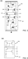
- FIG. 3 schematically illustrates an improved strain sensor 300.
- FIG. 3 provides a circuit diagram of the improved strain sensor 300.
- the improved strain sensor 300 also comprises a sensing circuit 301 and a complementary circuit 302.
- the sensing circuit 301 is in the form of a nonlinear current mirror in cascode configuration.
- the complementary circuit 302 of the improved strain sensor 300 is in the form of a linear current mirror in cascode configuration.
- the sensing circuit 301 of the improved strain sensor 300 corresponds with the sensing circuit 101 of the basic strain sensor 100 except for some particularities.
- the sensing circuit 301 of the improved strain sensor 300 comprises a resistance-providing transistor 307 which. in effect, substitutes the resistance 109 represented in FIG. 1 .
- the resistance-providing transistor 307 may be biased at a zero temperature coefficient point.
- the resistance-providing transistor 307 may operate in a linear regime, although operation a saturation regime is also possible.
- the resistance-providing transistor 307 may be formed by an assembly of transistors, which may be coupled in parallel, for example, and oriented such that a resistance is provided that is relatively insensitive to strain. This prevents the resistance from significantly affecting strain sensing. Alternatively, transistors may be oriented such that that the resistance contributes to strain sensing.
- the sensing circuit 301 of the improved strain sensor 300 comprises a pair of cascode transistors 303, 304, which have been added with respect to the sensing circuit 101 of the basic strain sensor 100.
- One of the cascode transistors 303 operates as a diode and is coupled in series with another transistor 305 that operates as a diode, which corresponds to the input transistor 107 in the sensing circuit 101 of the basic strain sensor 100.
- the other cascode transistor 304 is in a common gate configuration and is coupled in series with another transistor 306 that is in a common source configuration, which corresponds to the output transistor 108 in the sensing circuit 101 of the basic strain sensor 100.
- the complementary circuit 302 of the improved strain sensor 300 corresponds with the complementary circuit 102 of the basic strain sensor 100 to which a pair of cascode transistors 308, 309 have been added.
- One of the cascode transistors 308 operates as a diode and is coupled in series with another transistor 310 that operates as a diode.
- the other cascode transistor 309 is in a common gate configuration and is coupled in series with another transistor 311 that is in a common source configuration.
- the improved strain sensor 300 operates like the basic strain sensor 100 described hereinbefore.
- a left branch current 312 flows out from the complementary circuit 302 into the sensing circuit 301.
- a right branch current 313 flows out from the sensing circuit 301 into the complementary circuit 302.
- the improved strain sensor 300 reaches an operating state. At this point, the left branch current 312 and the right branch current 313 are in a relationship to each other that corresponds to the transfer function of the sensing circuit 301 and that of the complementary circuit 302.
- the operating state is insensitive to supply voltage variations, as well as to temperature variations.
- the improved strain sensor 300 may be even less sensitive to variations in the supply voltage than the basic strain sensor 100. That is, these variations, which may comprise noise, may be suppressed to a greater extent. This is due to the cascode transistors 303, 304, 308, 309 mentioned hereinbefore, which counter a so-called Early effect in transistors 305, 306, 310, 311 in the improved strain sensor 300.
- FIG. 4 schematically illustrates a strain sensor assembly 400.
- FIG. 4 provides a circuit diagram of the strain sensor assembly 400.
- the strain sensor assembly 400 comprises two strain sensors: a first strain sensor 401 and a second strain sensor 402.
- the first strain sensor 401 corresponds to the improved strain sensor 300 described hereinbefore with reference to FIG. 3 .
- the first strain sensor 401 and the second strain sensor 402 are mirrored versions of each other.
- the strain sensor assembly 400 further comprises a differential output stage 403 and two start-up circuits 404, 405: a first start-up circuit 404 for the first strain sensor 401 and a second start-up circuit 405 for the second strain sensor 402.
- the differential output stage 403 comprises a first current-mirroring circuit 406 that is coupled to the first strain sensor 401 and a second current-mirroring circuit 407 that is coupled to the second strain sensor 402.
- Each of these current-mirroring circuits 406, 407 comprises two transistors in cascode configuration.
- the first current-mirroring circuit 406 and the second current-mirroring circuit 407 are jointly is coupled to a current subtraction node 408 in the differential output stage 403.
- the differential output stage 403 further comprises an output current mirror 409 in cascode configuration.
- An input of the output current mirror 409 is coupled to the current subtraction node 408.
- An output of the of output current mirror 409 is coupled to an output node 410 of the differential output stage 403, which also constitutes an output node 410 of the strain sensor assembly 400.
- An output transistor 411 provides a resistance between the output node 410 and signal ground.
- the strain sensor assembly 400 basically operates as follows.
- the first strain sensor 401 and the second strain sensor 402 reach an operating state as described hereinbefore with respect to the improved strain sensor 300 illustrated in FIG. 3 .
- the first strain sensor 401 provides a left branch current 412 that varies as a function of strain.
- the first current-mirroring circuit 406 mirrors this left branch current 412 to the current subtraction node 408.
- the second strain sensor 402 provides a right branch current 413 that also varies as a function of strain, but inversely with respect to the left branch current 412 in the first strain sensor 401.
- the second current-mirroring circuit 407 mirrors this right branch current 413 to the current subtraction node 408;
- the current subtraction node 408 thus receives two currents that both vary as a function of strain, but inversely with respect to each other.
- a differential current which is a subtraction of these two currents, flows into the input of the output current mirror 409.
- a mirrored differential current thus flows from the output of the output current mirror 409 into the resistance provided by the output transistor 411. Accordingly, this produces an output voltage at the output node 410 of the strain sensor assembly 400.
- the output voltage varies as a function of strain. More specifically, the output voltage reflects a differential mode strain measurement jointly accomplished by the first strain sensor 401 and the second strain sensor 402, which, in fact, form a differential pair.
- This differential mode strain measurement is relatively precise and accurate because the output voltage is relatively insensitive to supply voltage variations, as well as temperature variations, as explained hereinbefore with respect to the basic strain sensor 100 illustrated in FIG. 1 .
- the strain sensor assembly 400 may be comprised in, for example, an integrated circuit.
- the integrated circuit may comprise, for example, a transmission circuit capable of wirelessly transmitting strain measurement data to another device in a measurement system.
- the measurement system may be in the form of, for example, a so-called Internet of things infrastructure.
- the measurement system may comprise a device that emits a power signal that allows wirelessly powering the basic strain sensor 100.
- the integrated circuit, or any other entity of which the strain sensor assembly 400 forms part may comprise an energy harvesting circuit that generates a power supply voltage for the basic strain sensor 100 on the basis of the power signal received.
- the aforementioned remarks equally apply to other strain sensor embodiments, such as, for example, the basic strain sensor 100 illustrated in FIG. 1 and the improved strain sensor 300 illustrated in FIG. 3 .
- FIG. 5 schematically illustrates an alternative strain sensor 500.
- FIG. 5 provides a circuit diagram of the alternative strain sensor 500.
- the alternative strain sensor 500 also comprises a sensing circuit 501 and a complementary circuit 502.
- the aforementioned circuits 501, 502 jointly constitute a voltage reference circuit.
- the sensing circuit 501 comprises two transistors of the field-effect type that are oriented differently with respect to each other.
- the complementary circuit 502 comprises a current mirror circuit.
- the alternative strain sensor 500 provides a reference output voltage that varies as a function of strain, whereas the reference output voltage is insensitive to supply voltage variations as well as temperature variations. Thus, the alternative strain sensor 500 also allows precise and accurate strain measurement.
- the invention may be applied in numerous types of products or methods related to measuring physical forces.
- measurement of strain is mentioned.
- the embodiments presented hereinbefore, as well as other embodiments may be used for measuring another physical force, such as, for example, pressure.
- a sensor device may comprise a component that converts pressure into strain, which may be measured by a strain sensor in accordance with the invention.
- strain sensor should be understood in a broad sense. This term may embrace any entity capable of measuring a physical force that can be converted into strain.
- FIGS. 1-4 are based on a current reference circuit of the beta multiplier type.
- FIG; 5 another embodiment with reference to FIG; 5 has been presented, which is based on a voltage reference circuit.
- a strain sensor in accordance with the invention may be based on any type of reference circuit that includes a sub circuit having a transfer function that can be made strain dependent. This strain-sensitive sub-circuit then thus forms the sensing circuit in the strain sensor in accordance with the invention.
- strain-sensitive components in the sensing circuit need not necessarily be transistors.
- transistors in the sensing circuit need not necessarily be of the field-effect type.
- a transistor cascode configuration may differ from that in the embodiments presented with reference to FIGS. 3 and 4 .
Landscapes
- Physics & Mathematics (AREA)
- General Physics & Mathematics (AREA)
- Engineering & Computer Science (AREA)
- Power Engineering (AREA)
- Microelectronics & Electronic Packaging (AREA)
- Technology Law (AREA)
- Measurement Of Length, Angles, Or The Like Using Electric Or Magnetic Means (AREA)
Abstract
A strain sensor (100) comprises a sensing circuit (101) having a transfer function from an input (103) to an output (105) that varies as a function of strain exerted on the sensing circuit (101). The strain sensor (100) further comprises a complementary circuit (102) having an input (106) coupled to the output (105) of the sensing circuit (101) and an output (104) coupled to the input (103) of the sensing circuit (101). The complementary circuit (102) has a different transfer function from its input (106) to its output (105). The sensing circuit (101) and the complementary circuit (102) jointly form a reference circuit that reaches an operating state. The operating state is defined by the transfer function of the sensing circuit (101) and the different transfer function of the complementary circuit (102). The operating state is, at least at first order, at least supply-voltage independent. The strain sensor (100) provides an output signal (201, 202) corresponding with the operating state, which varies as a function of the strain.
Description
- An aspect of the invention relates to a strain sensor. The strain sensor may be used, for example, to monitor structural health of a mechanical construction. Further aspects of the invention relate to a strain sensor assembly, an integrated circuit, and a measurement system..
- Strain is an important parameter in monitoring structural health of mechanical constructions, such as, for example, windmills, buildings, bridges, pipelines, cables, and so on. Measuring strain allows predicting possible damage to a mechanical structure. In order to measure strain, the mechanical structure may be provided with a strain sensor at a point of interest to be monitored. There may be various points of interest to be monitored in the mechanical structure, or in a group of such structures. Thus, there may be a whole set of strain sensors for monitoring structural health. In order to facilitate monitoring structural health, a so-called Internet of things network may be deployed that includes the strain sensors.
- Patent publication
EP0363005A2 describes a sensor that includes a field-effect transistor formed on GaAs for sensing a stress. The field-effect transistor is driven by a constant current or a constant voltage so as to detect a change of an electrical characteristic, such as threshold, due to a stress. When a stress is applied to the field-effect transistor, the transconductance changes, and the temperature changes, consequently the I-V characteristic changes. An AC signal biased by a direct current is supplied to the gate of the field-effect transistor. A drain current is detected in an AC component and a DC component so as to detect a temperature concurrently with a detection of a stress. - There is a need for an improved strain sensor that allows better performance in at least one of the following aspects: sensitivity, precision, and accuracy.
- In accordance with an aspect of the invention as defined in claim 1, there is provided a strain sensor comprising:
- a sensing circuit having a transfer function from an input to an output that varies as a function of strain exerted on the sensing circuit,
- a complementary circuit having an input coupled to the output of the sensing circuit and an output coupled to the input of the sensing circuit, the complementary circuit having a different transfer function from its input to its output so that the sensing circuit and the complementary circuit jointly form a reference circuit that reaches an operating state that, at least at first order, is at least supply-voltage independent, the operating state being defined by the transfer function of the sensing circuit and the different transfer function of the complementary circuit, the strain sensor providing an output signal corresponding with the operating state, which varies as a function of the strain.
- Such a strain sensor is relatively insensitive to supply voltage variations and, in addition, may also be relatively insensitive to temperature variations. Thus, a relatively high precision and a relatively high accuracy in strain measurement may be achieved. What is more, relatively high sensitivity may also be achieved, in particular compared with conventional metallic strain gauges. A gauge factor about 1000 may be achieved with a strain sensor as defined hereinbefore, whereas the gauge factor of metallic strain gauges is several orders of magnitude lower, limited to about 2. Moreover, a strain sensor as defined hereinbefore may provide a relatively linear measurement characteristic with negligible hysteresis. This allows a relatively simple two-point calibration.
- Another advantage is that the strain sensor as defined hereinbefore may operate with low power consumption. This may be even down to a level where the strain sensor can be wirelessly powered, obviating a need for on-board batteries or other energy sources. For example, the strain sensor may be wirelessly powered by a radiofrequency signal, light, vibration, thermal energy, or another environmental energy source that a transducer circuit may convert into electrical power. This makes that the strain sensor is particularly suited to form part of an Internet of things network, which may be wireless.
- Moreover, the strain sensor as defined hereinbefore may be relatively small in size and may have a low form factor. This and the low power consumption also makes the strain sensor suitable for applications in, for example, wearable and implanted biomedical devices. In addition, the strain sensor can be manufactured at relatively low cost, which further favors a wide range of applications.
- In accordance with a further aspect of the invention as defined in claim 12, there is provided a strain sensor assembly comprising:
- a first strain sensor as defined hereinbefore of which the output signal varies as a function of the strain;
- a second strain sensor as defined hereinbefore of which the output signal varies as a function of the strain but inversely with respect to that of the first strain sensor: and
- a differential output stage arranged to provide an output signal that corresponds with a difference between the output signal of the first strain sensor and the output signal of the second strain sensor.
- In accordance with yet further aspects of the invention, there is provided an integrated circuit as defined in claim 14, and a measurement system as defined in claim 15.
- For the purpose of illustration, some embodiments of the invention are described in detail with reference to accompanying drawings. In this description, additional features will be presented, some of which are defined in the dependent claims, and advantages will be apparent.
-
-
FIG. 1 is a circuit diagram of a basic strain sensor. -
FIG. 2 is a graph in which two transfer functions within the basic strain sensor are plotted. -
FIG. 3 is a circuit diagram of an improved strain sensor. -
FIG. 4 is a circuit diagram of a strain sensor assembly that includes two improved strain sensors. -
FIG. 5 is a circuit diagram of an alternative strain sensor. -
FIG. 1 schematically illustrates abasic strain sensor 100.FIG. 1 provides a circuit diagram of thebasic strain sensor 100. Thebasic strain sensor 100 may be fixed to a physical entity that may undergo strain, such as, for example, a structure or a body. Thebasic strain sensor 100 may be fixed so that any strain that the physical entity undergoes is transferred to thebasic strain sensor 100. - The
basic strain sensor 100 comprises asensing circuit 101 and acomplementary circuit 102. Aninput 103 of thesensing circuit 101 is coupled to anoutput 104 of thecomplementary circuit 102. Anoutput 105 of thesensing circuit 101 is coupled to aninput 106 of thecomplementary circuit 102. Thesensing circuit 101 and thecomplementary circuit 102 thus form a loop. Thebasic strain sensor 100 may further comprise a startup circuit, which is not represented inFIG. 1 for the sake of simplicity and convenience. - In this embodiment, the
sensing circuit 101 is in the form of a non-linear current-mirror circuit. The non-linear current mirror circuit has aninput transistor 107 that operates as a diode, and anoutput transistor 108 in a common source configuration. Theinput transistor 107 and theoutput transistor 108 may be of the field-effect type. These twotransistors sensing circuit 101. More specifically, theinput transistor 107 and theoutput transistor 108 may be oriented perpendicularly with respect to each other. These transistors may be oriented along particular crystallographic directions of a semiconductor substrate for best strain sensing performance. - The non-linear current mirror circuit comprises a
resistance 109 that is coupled between a source of theoutput transistor 108 and a common circuit node, whereas a source of theinput transistor 107 is directly coupled to the common circuit node. The , common circuit node may be, for example, a supply voltage line and may constitute signal ground. Theresistance 109 may be provided by a transistor, or an assembly of transistors, as will be illustrated further on. - In this embodiment, the
complementary circuit 102 is in the form of a linear current mirror circuit. Thesensing circuit 101 and thecomplementary circuit 102 jointly form a current reference circuit of the beta multiplier type. Thebasic strain sensor 100 illustrated inFIG. 1 may therefore be regarded as a beta (β) multiplier current reference circuit in which two field-effect transistors effect transistors -
FIG. 2 illustrates two transfer functions in thebasic strain sensor 100.FIG. 2 provides agraph 200 having a horizontal axis that represents a direct current 201 flowing from theoutput 104 of thecomplementary circuit 102 in theinput 103 of thesensing circuit 101, as indicated inFIG. 1 . A vertical axis represents a direct current 202 flowing from theoutput 105 of thesensing circuit 101 into theinput 106 of thecomplementary circuit 102, as indicated inFIG. 1 . The direct current 201 that is represented by the horizontal axis will be referred to hereinafter as left branch current 201 for reasons of convenience. The left branch current 201 is an input current of thesensing circuit 101, as well as an output current of thecomplementary circuit 102. The direct current 202 that is represented by the vertical axis will be referred to hereinafter asright branch current 202 for reasons of convenience. Theright branch current 202 is an output current of thesensing circuit 101, as well as an input current of thecomplementary circuit 102. - The graph in
FIG. 2 comprises twocurves first curve 203 represents a transfer function of thesensing circuit 101. Asecond curve 203 represents a transfer function of thecomplementary circuit 102 and, more precisely, represents the inverse thereof. In other words, thefirst curve 203 represents a relationship between theright branch current 202 and the left branch current 201 defined thesensing circuit 101. Thesecond curve 203 represents a relationship between the left branch current 201 and the right branch current 202 defined by thecomplementary circuit 102. -
FIG. 2 illustrates that the transfer function of thesensing circuit 101 is different from the transfer function of thecomplementary circuit 102. The transfer function of thesensing circuit 101 is nonlinear, whereas the transfer function of thecomplementary circuit 102 is substantially linear. The transfer function of thesensing circuit 101 is nonlinear due to theresistance 109 between the source of theoutput transistor 108 and signal ground. Theresistance 109 makes that the transfer function of thesensing circuit 101 has at least a higher order term, such as a quadratic term. The quadratic term is dominant if a voltage drop across theresistance 109 is larger than the square root of a current flowing through theoutput transistor 108 multiplied by two divided by a gain parameter β of theoutput transistor 108. The aforementioned current corresponds with the right branch current 202 represented by the vertical axis of the graphFIG. 2 . - The
basic strain sensor 100 basically operate as follows. Thebasic strain sensor 100 reaches anoperating state 205 indicated inFIG. 2 . The operatingstate 205 is a point where the transfer function of thesensing circuit 101 intersects with the inverse of the transfer function of the complementary circuit. In theoperating state 205, the left branch current 201 and the right branch current 202 are in a relationship to each other that is in accordance with the transfer function of thesensing circuit 101 and that of thecomplementary circuit 102. The operatingstate 205 may therefore be regarded as an equilibrium state, which depends on the aforementioned transfer functions. It is assumed that the startup circuit mentioned hereinbefore, but not represented inFIG. 1 , prevents thebasic strain sensor 100 from reaching an operating state at which the aforementioned currents are all zero. - The transfer function of the
sensing circuit 101, represented by thefirst curve 203, varies as a function of the strain that is exerted on thesensing circuit 101. This is because the twotransistors sensing circuit 101 exhibit a piezoresistive effect and thetransistors transistors transistors transistors sensing circuit 101 depends on a ratio between the respective gain parameters β, the transfer function thus varies as a function of strain. - Since the transfer function of the
sensing circuit 101 varies as a function of strain, the operatingstate 205 also varies as a function of strain. Accordingly, theright branch current 202 and the left branch current 201 in the strain sensor, which depend on theoperating state 205, also vary as a function of strain. Thus, a value of either of the aforementioned currents represents a degree of strain that thesensing circuit 101 undergoes. The value of theright branch current 202, or that of the left branch current 201, or both, may be read out by means of a further current mirror circuit, which is not represented inFIG. 1 for the sake of simplicity and convenience. - Sensitivity to strain may be improved if the transfer function of the
complementary circuit 102 also varies as a function of strain, but inversely with respect to the transfer function of thesensing circuit 101. In this embodiment, this may be achieved by orienting two transistors that make up the linear current mirror also differently with respect to each other, but also differently with respect to the twotransistors sensing circuit 101. - Importantly, the
right branch current 202 and the left branch current 201, which vary as a function of strain, are at least at first order, supply-voltage independent. That is, variations in the supply voltage, such as, for example, noise, are effectively suppressed. Moreover, theright branch current 202 and the left branch current 201 are also relatively insensitive to temperature variations. All this contributes to precise and accurate strain measurement by reading out theright branch current 202, or the left branch current 201, or both. -
FIG. 3 schematically illustrates animproved strain sensor 300.FIG. 3 provides a circuit diagram of theimproved strain sensor 300. Theimproved strain sensor 300 also comprises asensing circuit 301 and acomplementary circuit 302. Thesensing circuit 301 is in the form of a nonlinear current mirror in cascode configuration. Thecomplementary circuit 302 of theimproved strain sensor 300 is in the form of a linear current mirror in cascode configuration. - In fact, the
sensing circuit 301 of theimproved strain sensor 300 corresponds with thesensing circuit 101 of thebasic strain sensor 100 except for some particularities. Thesensing circuit 301 of theimproved strain sensor 300 comprises a resistance-providingtransistor 307 which. in effect, substitutes theresistance 109 represented inFIG. 1 . The resistance-providingtransistor 307 may be biased at a zero temperature coefficient point. The resistance-providingtransistor 307 may operate in a linear regime, although operation a saturation regime is also possible. It should be noted that the resistance-providingtransistor 307 may be formed by an assembly of transistors, which may be coupled in parallel, for example, and oriented such that a resistance is provided that is relatively insensitive to strain. This prevents the resistance from significantly affecting strain sensing. Alternatively, transistors may be oriented such that that the resistance contributes to strain sensing. - The
sensing circuit 301 of theimproved strain sensor 300 comprises a pair ofcascode transistors sensing circuit 101 of thebasic strain sensor 100. One of thecascode transistors 303 operates as a diode and is coupled in series with anothertransistor 305 that operates as a diode, which corresponds to theinput transistor 107 in thesensing circuit 101 of thebasic strain sensor 100. Theother cascode transistor 304 is in a common gate configuration and is coupled in series with anothertransistor 306 that is in a common source configuration, which corresponds to theoutput transistor 108 in thesensing circuit 101 of thebasic strain sensor 100. - Likewise, the
complementary circuit 302 of theimproved strain sensor 300 corresponds with thecomplementary circuit 102 of thebasic strain sensor 100 to which a pair ofcascode transistors cascode transistors 308 operates as a diode and is coupled in series with anothertransistor 310 that operates as a diode. Theother cascode transistor 309 is in a common gate configuration and is coupled in series with anothertransistor 311 that is in a common source configuration. - The
improved strain sensor 300 operates like thebasic strain sensor 100 described hereinbefore. A left branch current 312 flows out from thecomplementary circuit 302 into thesensing circuit 301. A right branch current 313 flows out from thesensing circuit 301 into thecomplementary circuit 302. Theimproved strain sensor 300 reaches an operating state. At this point, the left branch current 312 and the right branch current 313 are in a relationship to each other that corresponds to the transfer function of thesensing circuit 301 and that of thecomplementary circuit 302. The operating state is insensitive to supply voltage variations, as well as to temperature variations. - The
improved strain sensor 300 may be even less sensitive to variations in the supply voltage than thebasic strain sensor 100. That is, these variations, which may comprise noise, may be suppressed to a greater extent. This is due to thecascode transistors transistors improved strain sensor 300. -
FIG. 4 schematically illustrates astrain sensor assembly 400.FIG. 4 provides a circuit diagram of thestrain sensor assembly 400. Thestrain sensor assembly 400 comprises two strain sensors: afirst strain sensor 401 and asecond strain sensor 402. Thefirst strain sensor 401 corresponds to theimproved strain sensor 300 described hereinbefore with reference toFIG. 3 . The same applies to thesecond strain sensor 402. Thefirst strain sensor 401 and thesecond strain sensor 402 are mirrored versions of each other. Thestrain sensor assembly 400 further comprises adifferential output stage 403 and two start-upcircuits 404, 405: a first start-upcircuit 404 for thefirst strain sensor 401 and a second start-upcircuit 405 for thesecond strain sensor 402. - In more detail, the
differential output stage 403 comprises a first current-mirroring circuit 406 that is coupled to thefirst strain sensor 401 and a second current-mirroring circuit 407 that is coupled to thesecond strain sensor 402. Each of these current-mirroringcircuits mirroring circuit 406 and the second current-mirroring circuit 407 are jointly is coupled to acurrent subtraction node 408 in thedifferential output stage 403. Thedifferential output stage 403 further comprises an outputcurrent mirror 409 in cascode configuration. An input of the outputcurrent mirror 409 is coupled to thecurrent subtraction node 408. An output of the of outputcurrent mirror 409 is coupled to anoutput node 410 of thedifferential output stage 403, which also constitutes anoutput node 410 of thestrain sensor assembly 400. Anoutput transistor 411 provides a resistance between theoutput node 410 and signal ground. - The
strain sensor assembly 400 basically operates as follows. Thefirst strain sensor 401 and thesecond strain sensor 402 reach an operating state as described hereinbefore with respect to theimproved strain sensor 300 illustrated inFIG. 3 . Accordingly, thefirst strain sensor 401 provides a left branch current 412 that varies as a function of strain. The first current-mirroring circuit 406 mirrors this left branch current 412 to thecurrent subtraction node 408. Thesecond strain sensor 402 provides a right branch current 413 that also varies as a function of strain, but inversely with respect to the left branch current 412 in thefirst strain sensor 401. The second current-mirroring circuit 407 mirrors this right branch current 413 to thecurrent subtraction node 408; - The
current subtraction node 408 thus receives two currents that both vary as a function of strain, but inversely with respect to each other. A differential current, which is a subtraction of these two currents, flows into the input of the outputcurrent mirror 409. A mirrored differential current thus flows from the output of the outputcurrent mirror 409 into the resistance provided by theoutput transistor 411. Accordingly, this produces an output voltage at theoutput node 410 of thestrain sensor assembly 400. The output voltage varies as a function of strain. More specifically, the output voltage reflects a differential mode strain measurement jointly accomplished by thefirst strain sensor 401 and thesecond strain sensor 402, which, in fact, form a differential pair. This differential mode strain measurement is relatively precise and accurate because the output voltage is relatively insensitive to supply voltage variations, as well as temperature variations, as explained hereinbefore with respect to thebasic strain sensor 100 illustrated inFIG. 1 . - The
strain sensor assembly 400 may be comprised in, for example, an integrated circuit. The integrated circuit may comprise, for example, a transmission circuit capable of wirelessly transmitting strain measurement data to another device in a measurement system. The measurement system may be in the form of, for example, a so-called Internet of things infrastructure. The measurement system may comprise a device that emits a power signal that allows wirelessly powering thebasic strain sensor 100. To that end, the integrated circuit, or any other entity of which thestrain sensor assembly 400 forms part, may comprise an energy harvesting circuit that generates a power supply voltage for thebasic strain sensor 100 on the basis of the power signal received. The aforementioned remarks equally apply to other strain sensor embodiments, such as, for example, thebasic strain sensor 100 illustrated inFIG. 1 and theimproved strain sensor 300 illustrated inFIG. 3 . -
FIG. 5 schematically illustrates analternative strain sensor 500.FIG. 5 provides a circuit diagram of thealternative strain sensor 500. Thealternative strain sensor 500 also comprises asensing circuit 501 and acomplementary circuit 502. In this embodiment, theaforementioned circuits sensing circuit 501 comprises two transistors of the field-effect type that are oriented differently with respect to each other. Thecomplementary circuit 502 comprises a current mirror circuit. Thealternative strain sensor 500 provides a reference output voltage that varies as a function of strain, whereas the reference output voltage is insensitive to supply voltage variations as well as temperature variations. Thus, thealternative strain sensor 500 also allows precise and accurate strain measurement. - The embodiments described hereinbefore with reference to the drawings are presented by way of illustration. The invention may be implemented in numerous different ways. In order to illustrate this, some alternatives are briefly indicated.
- The invention may be applied in numerous types of products or methods related to measuring physical forces. In the embodiments presented hereinbefore, measurement of strain is mentioned. However, the embodiments presented hereinbefore, as well as other embodiments, may be used for measuring another physical force, such as, for example, pressure. For example, a sensor device may comprise a component that converts pressure into strain, which may be measured by a strain sensor in accordance with the invention. Thus, the term "strain sensor" should be understood in a broad sense. This term may embrace any entity capable of measuring a physical force that can be converted into strain.
- There are numerous different ways of implementing a strain sensor in accordance with the invention. Various embodiments have been presented with reference to
FIGS. 1-4 , which are based on a current reference circuit of the beta multiplier type. In addition, another embodiment with reference toFIG; 5 has been presented, which is based on a voltage reference circuit. This is to illustrate that a strain sensor in accordance with the invention may be based on any type of reference circuit that includes a sub circuit having a transfer function that can be made strain dependent. This strain-sensitive sub-circuit then thus forms the sensing circuit in the strain sensor in accordance with the invention. Moreover, strain-sensitive components in the sensing circuit need not necessarily be transistors. Furthermore, transistors in the sensing circuit need not necessarily be of the field-effect type. Alternatives include, for example, bipolar transistors, high-electron-mobility (HEMT) transistors, and heterojunction bipolar (HBT) transistors. A transistor cascode configuration may differ from that in the embodiments presented with reference toFIGS. 3 and4 . - The remarks made hereinbefore demonstrate that the embodiments described with reference to the drawings illustrate the invention, rather than limit the invention. The invention can be implemented in numerous alternative ways that are within the scope of the appended claims. All changes that come within the meaning and range of equivalency of the claims are to be embraced within their scope. Any reference sign in a claim should not be construed as limiting the claim. The verb "comprise" in a claim does not exclude the presence of other elements or other steps than those listed in the claim. The same applies to similar verbs such as "include" and "contain". The mention of an element in singular in a claim pertaining to a product, does not exclude that the product may comprise a plurality of such elements. Likewise, the mention of a step in singular in a claim pertaining to a method does not exclude that the method may comprise a plurality of such steps. The mere fact that respective dependent claims define respective additional features, does not exclude combinations of additional features other than those reflected in the claims.
Claims (15)
- A strain sensor (100, 300) comprising:- a sensing circuit (101, 301) having a transfer function from an input (103) to an output (105) that varies as a function of strain exerted on the sensing circuit,wherein the strain sensor further comprises:- a complementary circuit (102, 302) having an input (106) coupled to the output of the sensing circuit and an output (105) coupled to the input of the sensing circuit, the complementary circuit having a different transfer function from its input to its output so that the sensing circuit and the complementary circuit jointly form a reference circuit that reaches an operating state (205) that, at least at first order, is at least supply-voltage independent, the operating state being defined by the transfer function of the sensing circuit and the different transfer function of the complementary circuit, the strain sensor providing an output signal (201, 202; 312, 313) corresponding with the operating state, which varies as a function of the strain.
- A strain sensor according to claim 1, wherein the different transfer function of the complementary circuit (102, 302) also varies as a function of strain but inversely with respect to the transfer function of the sensing circuit (101, 301).
- A strain sensor according to any of claims 1 and 2, wherein the sensing circuit (101, 301) comprises two transistors of the field-effect type (107, 108; 305, 306) that affect the transfer function of the sensing circuit, the two transistors being oriented differently with respect to each other in the sensing circuit.
- A strain sensor according to claim 3, wherein the sensing circuit (101, 301) comprises a non-linear current-mirror circuit having an input transistor (107, 305) that operates as a diode, and an output transistor (108, 306) in a common source configuration with a resistance (109, 307) between source and a common circuit node making that transfer function of the sensing circuit is non-linear.
- A strain sensor according to claim 4, wherein the resistance (307) is provided by at least one transistor of the field-effect type.
- A strain sensor according to claim 5, wherein the transistor that provides the resistance (307) is biased at a zero temperature coefficient point.
- A strain sensor according to any of claims 5 and 6, wherein the transistor that provides the resistance (307) configured to operate in a linear regime.
- A strain sensor according to any of claims 3 to 6, wherein the complementary circuit (102, 302) comprises a linear current-mirror circuit, whereby the sensing circuit (101, 301) and the complementary circuit jointly form a current reference circuit of the beta multiplier type.
- A strain sensor according to any of claims 4 to 8, wherein the non-linear current-mirror circuit in the sensing circuit (301) has a cascode configuration.
- A strain sensor according to any of claims 8 to 9, wherein the linear current-mirror circuit in the complementary circuit (302) has a cascode configuration..
- A strain sensor according to any of claims 3 to 10, wherein the two transistors (107, 108; 305, 306) of the sensing circuit (101, 301) are oriented perpendicularly with respect to each other.
- A strain sensor assembly (400) comprising:- a first strain sensor (401) according to any of claims 1 to 11 of which the output signal varies as a function of the strain;- a second strain sensor (402) according to any of claims 1 to 11, of which the output signal varies as a function of the strain but inversely with respect to that of the first strain sensor: and- a differential output stage (403) arranged to provide an output signal that corresponds with a difference between the output signal of the first strain sensor and the output signal of the second strain sensor.
- A strain sensor assembly according to claim to 12, wherein the first strain sensor (401) and the second strain sensor (402) are mirrored versions of each other.
- An integrated circuit comprising at least one of the following: a strain sensor according (100, 300) to any of claims 1 to 11, and a strain sensor assembly (400) according to any of claims 12 and 13.
- A measurement system comprising at least one of the following: a strain sensor according (100, 300) to any of claims 1 to 11, and a strain sensor assembly (400) according to any of claims 12 and 13.
Priority Applications (4)
| Application Number | Priority Date | Filing Date | Title |
|---|---|---|---|
| EP20188775.9A EP3945299A1 (en) | 2020-07-30 | 2020-07-30 | Strain sensor |
| PCT/EP2021/071499 WO2022023571A1 (en) | 2020-07-30 | 2021-07-30 | Strain sensor |
| US18/016,902 US12442698B2 (en) | 2020-07-30 | 2021-07-30 | Strain sensor |
| EP21752557.5A EP4189350B1 (en) | 2020-07-30 | 2021-07-30 | Strain sensor |
Applications Claiming Priority (1)
| Application Number | Priority Date | Filing Date | Title |
|---|---|---|---|
| EP20188775.9A EP3945299A1 (en) | 2020-07-30 | 2020-07-30 | Strain sensor |
Publications (1)
| Publication Number | Publication Date |
|---|---|
| EP3945299A1 true EP3945299A1 (en) | 2022-02-02 |
Family
ID=71894761
Family Applications (2)
| Application Number | Title | Priority Date | Filing Date |
|---|---|---|---|
| EP20188775.9A Withdrawn EP3945299A1 (en) | 2020-07-30 | 2020-07-30 | Strain sensor |
| EP21752557.5A Active EP4189350B1 (en) | 2020-07-30 | 2021-07-30 | Strain sensor |
Family Applications After (1)
| Application Number | Title | Priority Date | Filing Date |
|---|---|---|---|
| EP21752557.5A Active EP4189350B1 (en) | 2020-07-30 | 2021-07-30 | Strain sensor |
Country Status (3)
| Country | Link |
|---|---|
| US (1) | US12442698B2 (en) |
| EP (2) | EP3945299A1 (en) |
| WO (1) | WO2022023571A1 (en) |
Cited By (1)
| Publication number | Priority date | Publication date | Assignee | Title |
|---|---|---|---|---|
| US20220404217A1 (en) * | 2021-06-16 | 2022-12-22 | Robert Bosch Gmbh | Stress and/or strain measurement cell for a stress and/or strain measurement system |
Citations (2)
| Publication number | Priority date | Publication date | Assignee | Title |
|---|---|---|---|---|
| JPS5748607A (en) * | 1980-09-09 | 1982-03-20 | Fuji Electric Co Ltd | Pressure transducer |
| EP0363005A2 (en) | 1988-09-02 | 1990-04-11 | Honda Giken Kogyo Kabushiki Kaisha | A semiconductor sensor |
Family Cites Families (5)
| Publication number | Priority date | Publication date | Assignee | Title |
|---|---|---|---|---|
| US6121823A (en) * | 1999-03-17 | 2000-09-19 | Analytical Technology, Inc. | Electrical circuit for sensors requiring a variety of bias voltages |
| US10468002B2 (en) * | 2017-04-26 | 2019-11-05 | Ron Lewis Schille | Programmable electronic harmonica having bifurcated air channels |
| CN110274703A (en) * | 2019-07-12 | 2019-09-24 | 广州芯世物科技有限公司 | A kind of the CMOS temperature-sensitive circuit and temperature sensor of high sensitivity |
| GB2627890B (en) * | 2020-04-21 | 2025-03-12 | Cirrus Logic Int Semiconductor Ltd | Force sensing systems |
| US11415405B2 (en) * | 2020-04-24 | 2022-08-16 | STMicroelectronics Asia Pacific Ptd Ltd | Strain gauge having unbalanced bias for single sided applications |
-
2020
- 2020-07-30 EP EP20188775.9A patent/EP3945299A1/en not_active Withdrawn
-
2021
- 2021-07-30 EP EP21752557.5A patent/EP4189350B1/en active Active
- 2021-07-30 US US18/016,902 patent/US12442698B2/en active Active
- 2021-07-30 WO PCT/EP2021/071499 patent/WO2022023571A1/en not_active Ceased
Patent Citations (2)
| Publication number | Priority date | Publication date | Assignee | Title |
|---|---|---|---|---|
| JPS5748607A (en) * | 1980-09-09 | 1982-03-20 | Fuji Electric Co Ltd | Pressure transducer |
| EP0363005A2 (en) | 1988-09-02 | 1990-04-11 | Honda Giken Kogyo Kabushiki Kaisha | A semiconductor sensor |
Non-Patent Citations (2)
| Title |
|---|
| CHI-HSIUNG WANG ET AL: "Supply voltage and temperature insensitive current reference for the 4 MHz oscillator", INTEGRATED CIRCUITS (ISIC), 2011 13TH INTERNATIONAL SYMPOSIUM ON, IEEE, 12 December 2011 (2011-12-12), pages 35 - 38, XP032096186, ISBN: 978-1-61284-863-1, DOI: 10.1109/ISICIR.2011.6131873 * |
| WANG YEN-TING ET AL: "A CMOS supply-insensitive with 13ppm/°C temperature coefficient current reference", 2013 IEEE 56TH INTERNATIONAL MIDWEST SYMPOSIUM ON CIRCUITS AND SYSTEMS (MWSCAS), IEEE, 3 August 2014 (2014-08-03), pages 475 - 478, XP032648801, ISSN: 1548-3746, ISBN: 978-1-4799-4134-6, [retrieved on 20140923], DOI: 10.1109/MWSCAS.2014.6908455 * |
Cited By (2)
| Publication number | Priority date | Publication date | Assignee | Title |
|---|---|---|---|---|
| US20220404217A1 (en) * | 2021-06-16 | 2022-12-22 | Robert Bosch Gmbh | Stress and/or strain measurement cell for a stress and/or strain measurement system |
| US11971316B2 (en) * | 2021-06-16 | 2024-04-30 | Robert Bosch Gmbh | Direction-dependent stress and/or strain measurement cell for a stress and/or strain measurement system |
Also Published As
| Publication number | Publication date |
|---|---|
| EP4189350A1 (en) | 2023-06-07 |
| EP4189350B1 (en) | 2026-04-15 |
| WO2022023571A1 (en) | 2022-02-03 |
| US20230296455A1 (en) | 2023-09-21 |
| US12442698B2 (en) | 2025-10-14 |
Similar Documents
| Publication | Publication Date | Title |
|---|---|---|
| EP2128579B1 (en) | Arrangement for linearizing a non-linear sensor | |
| CA2145698C (en) | Electronic circuit for a transducer | |
| US10393608B2 (en) | Pressure change measuring apparatus and pressure change measuring method | |
| CN110932690B (en) | Amplifier with common mode detection | |
| DE60139017D1 (en) | THIN FILM MAGNETIC SENSOR | |
| CN107003268B (en) | Control circuit for use with sensor and measurement system including the same | |
| CN1122631A (en) | Strain gauge sensor with full temperature signal | |
| US20040081224A1 (en) | Device for measuring temperature of semiconductor integrated circuit | |
| EP4189350B1 (en) | Strain sensor | |
| JP2002527767A (en) | Circuit arrangement for temperature non-linearity compensation of the characteristic curve of a piezoresistive measuring resistor connected in a bridge circuit | |
| US20070295095A1 (en) | Apparatus for providing an output proportional to pressure divided by temperature (P/T) | |
| US20050274187A1 (en) | Z-axis thermal accelerometer | |
| US8893554B2 (en) | System and method for passively compensating pressure sensors | |
| US10634565B2 (en) | Temperature sensing apparatus and temperature sensing method thereof | |
| JPH09105681A (en) | Temperature measurement circuit | |
| US6107861A (en) | Circuit for self compensation of silicon strain gauge pressure transmitters | |
| EP3860313B1 (en) | Temperature measurement from luminaire sensors | |
| EP0709660A1 (en) | Sensor and a method for temperature compensating for span variation in the sensor | |
| US12625012B2 (en) | Temperature sensor device | |
| JP2948958B2 (en) | Transducer circuit | |
| CN115901072B (en) | Compensation method and system for silicon piezoresistive air pressure sensing module | |
| Biswas et al. | Design of a Piezoresistive Microaccelerometer with high sensitivity for medical diagnostic | |
| EP3220156A1 (en) | Sensor device | |
| JP2001201413A (en) | Pressure sensor | |
| JPS61243338A (en) | Temperature compensation circuit for semiconductor prressure sensor |
Legal Events
| Date | Code | Title | Description |
|---|---|---|---|
| PUAI | Public reference made under article 153(3) epc to a published international application that has entered the european phase |
Free format text: ORIGINAL CODE: 0009012 |
|
| STAA | Information on the status of an ep patent application or granted ep patent |
Free format text: STATUS: THE APPLICATION HAS BEEN PUBLISHED |
|
| AK | Designated contracting states |
Kind code of ref document: A1 Designated state(s): AL AT BE BG CH CY CZ DE DK EE ES FI FR GB GR HR HU IE IS IT LI LT LU LV MC MK MT NL NO PL PT RO RS SE SI SK SM TR |
|
| STAA | Information on the status of an ep patent application or granted ep patent |
Free format text: STATUS: THE APPLICATION IS DEEMED TO BE WITHDRAWN |
|
| 18D | Application deemed to be withdrawn |
Effective date: 20220803 |